1
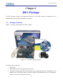
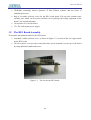
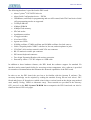
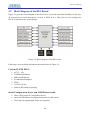
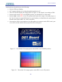
Altera DE1 Board
DE1
Development and Education Board
User Manual
Version 1.2.1
Copyright © 2012 Altera Corporation
Altera DE1 Board
CONTENTS
Chapter 1 DE1 Package.....................................................................................................................1
1.1
1.2
1.3
Package Contents .................................................................................................................1
The DE1 Board Assembly....................................................................................................2
Getting Help.........................................................................................................................3
Chapter 2 Altera DE1 Board.............................................................................................................4
2.1
2.2
Layout and Components ......................................................................................................4
Block Diagram of the DE1 Board........................................................................................6
2.3
Power-up the DE1 Board .....................................................................................................8
Chapter 3 DE1 Control Panel .........................................................................................................10
3.1
3.2
3.3
Control Panel Setup ...........................................................................................................10
Controlling the LEDs and 7-Segment Displays .................................................................12
Switches and Push-buttons.................................................................................................14
3.4
3.5
3.6
3.7
SDRAM/SRAM/Flash Controller and Programmer ..........................................................14
PS/2 Device........................................................................................................................16
SD Card..............................................................................................................................17
RS-232 Communication.....................................................................................................18
3.8
3.9
VGA ...................................................................................................................................19
Overall Structure of the DE1 Control Panel ......................................................................20
Chapter 4 Using the DE1 Board .....................................................................................................22
4.1
4.2
4.3
Configuring the Cyclone II FPGA .....................................................................................22
Using the LEDs and Switches............................................................................................24
Using the 7-segment Displays............................................................................................28
4.4
4.5
4.6
4.7
4.8
Clock Inputs .......................................................................................................................29
Using the Expansion Header..............................................................................................30
Using VGA ........................................................................................................................34
Using the 24-bit Audio CODEC ........................................................................................36
RS-232 Serial Port .............................................................................................................37
4.9
4.10
PS/2 Serial Port ..................................................................................................................38
Using SDRAM/SRAM/Flash.............................................................................................38
Chapter 5 Examples of Advanced Demonstrations ......................................................................44
5.1
5.2
DE1 Factory Configuration................................................................................................44
Music Synthesizer Demonstration .....................................................................................45
5.3
5.4
A Karaoke Machine ...........................................................................................................48
SD Card Music Player........................................................................................................50
ii
DE1 User Manual
Chapter 1
DE1 Package
The DE1 package contains all components needed to use the DE1 board in conjunction with a
computer that runs the Microsoft Windows software.
1.1
Package Contents
Figure 1.1 shows a photograph of the DE1 package.
Figure 1.1. The DE1 package contents.
The DE1 package includes:
•
•
•
DE1 board
USB Cable for FPGA programming and control
CD-ROM containing the DE1 documentation and supporting materials, including the User
Manual, the Control Panel utility, reference designs and demonstrations, device datasheets,
tutorials, and a set of laboratory exercises
1
DE1 User Manual
•
CD-ROMs containing Altera’s Quartus® II Web Edition software and the Nios® II
embedded processor
•
Bag of six rubber (silicon) covers for the DE1 board stands. The bag also contains some
extender pins, which can be used to facilitate easier probing with testing equipment of the
board’s I/O expansion headers
•
Clear plastic cover for the board
•
7.5V DC wall-mount power supply
1.2
The DE1 Board Assembly
To assemble the included stands for the DE1 board:
•
Assemble a rubber (silicon) cover, as shown in Figure 1.2, for each of the six copper stands
on the DE1 board
•
The clear plastic cover provides extra protection, and is mounted over the top of the board
by using additional stands and screws
Figure 1.2. The feet for the DE1 board.
2
DE1 User Manual
1.3
Getting Help
Here are the addresses where you can get help if you encounter problems:
•
Altera Corporation
101 Innovation Drive
San Jose, California, 95134 USA
Email: [email protected]
•
Terasic Technologies
9F., No.176, Sec.2, Gongdao 5th Rd, East Dist, Hsinchu City, 30070. Taiwan
Email: [email protected]
Web: www.de1.terasic.com
3
DE1 User Manual
Chapter 2
Altera DE1 Board
This chapter presents the features and design characteristics of the DE1 board.
2.1
Layout and Components
A photograph of the DE1 board is shown in Figure 2.1. It depicts the layout of the board and
indicates the location of the connectors and key components.
Figure 2.1. The DE1 board.
The DE1 board has many features that allow the user to implement a wide range of designed
circuits, from simple circuits to various multimedia projects.
4
DE1 User Manual
The following hardware is provided on the DE1 board:
•
Altera Cyclone® II 2C20 FPGA device
•
•
Altera Serial Configuration device – EPCS4
USB Blaster (on board) for programming and user API control; both JTAG and Active Serial
(AS) programming modes are supported
•
512-Kbyte SRAM
•
•
•
•
8-Mbyte SDRAM
4-Mbyte Flash memory
SD Card socket
4 pushbutton switches
•
•
•
•
10 toggle switches
10 red user LEDs
8 green user LEDs
50-MHz oscillator, 27-MHz oscillator and 24-MHz oscillator for clock sources
•
•
•
24-bit CD-quality audio CODEC with line-in, line-out, and microphone-in jacks
VGA DAC (4-bit resistor network) with VGA-out connector
RS-232 transceiver and 9-pin connector
•
•
•
PS/2 mouse/keyboard connector
Two 40-pin Expansion Headers with resistor protection
Powered by either a 7.5V DC adapter or a USB cable
In addition to these hardware features, the DE1 board has software support for standard I/O
interfaces and a control panel facility for accessing various components. Also, software is provided
for a number of demonstrations that illustrate the advanced capabilities of the DE1 board.
In order to use the DE1 board, the user has to be familiar with the Quartus II software. The
necessary knowledge can be acquired by reading the tutorials Getting Started with Altera’s DE1
Board and Quartus II Introduction (which exists in three versions based on the design entry method
used, namely Verilog, VHDL or schematic entry). These tutorials are provided in the directory
DE1_tutorials on the DE1 System CD-ROM that accompanies the DE1 board and can also be
found on Altera’s DE1 web pages.
5
DE1 User Manual
2.2
Block Diagram of the DE1 Board
Figure 2.2 gives the block diagram of the DE1 board. To provide maximum flexibility for the user,
all connections are made through the Cyclone II FPGA device. Thus, the user can configure the
FPGA to implement any system design.
Figure 2.2. Block diagram of the DE1 board.
Following is more detailed information about the blocks in Figure 2.2:
Cyclone II 2C20 FPGA
•
•
18,752 LEs
52 M4K RAM blocks
•
•
•
•
•
240K total RAM bits
26 embedded multipliers
4 PLLs
315 user I/O pins
FineLine BGA 484-pin package
Serial Configuration device and USB Blaster circuit
•
Altera’s EPCS4 Serial Configuration device
•
•
On-board USB Blaster for programming and user API control
JTAG and AS programming modes are supported
6
DE1 User Manual
SRAM
•
512-Kbyte Static RAM memory chip
•
•
Organized as 256K x 16 bits
Accessible as memory for the Nios II processor and by the DE1 Control Panel
SDRAM
•
•
•
8-Mbyte Single Data Rate Synchronous Dynamic RAM memory chip
Organized as 1M x 16 bits x 4 banks
Accessible as memory for the Nios II processor and by the DE1 Control Panel
Flash memory
•
•
•
4-Mbyte NOR Flash memory.
8-bit data bus
Accessible as memory for the Nios II processor and by the DE1 Control Panel
SD card socket
•
Provides SPI mode for SD Card access
•
Accessible as memory for the Nios II processor with the DE1 SD Card Driver
Pushbutton switches
•
•
•
4 pushbutton switches
Debounced by a Schmitt trigger circuit
Normally high; generates one active-low pulse when the switch is pressed
Toggle switches
•
•
10 toggle switches for user inputs
A switch causes logic 0 when in the DOWN (closest to the edge of the DE1 board) position
and logic 1 when in the UP position
Clock inputs
•
•
•
50-MHz oscillator
27-MHz oscillator
24-MHz oscillator
•
SMA external clock input
Audio CODEC
•
Wolfson WM8731 24-bit sigma-delta audio CODEC
•
Line-level input, line-level output, and microphone input jacks
7
DE1 User Manual
•
•
Sampling frequency: 8 to 96 KHz
Applications for MP3 players and recorders, PDAs, smart phones, voice recorders, etc.
VGA output
•
•
•
Uses a 4-bit resistor-network DAC
With 15-pin high-density D-sub connector
Supports up to 640x480 at 60-Hz refresh rate
•
Can be used with the Cyclone II FPGA to implement a high-performance TV Encoder
Serial ports
•
One RS-232 port
•
•
•
One PS/2 port
DB-9 serial connector for the RS-232 port
PS/2 connector for connecting a PS2 mouse or keyboard to the DE1 board
Two 40-pin expansion headers
•
72 Cyclone II I/O pins, as well as 8 power and ground lines, are brought out to two 40-pin
expansion connectors
•
•
40-pin header is designed to accept a standard 40-pin ribbon cable used for IDE hard drives
Resistor protection is provided
2.3
Power-up the DE1 Board
The DE1 board comes with a preloaded configuration bit stream to demonstrate some features of
the board. This bit stream also allows users to see quickly if the board is working properly. To
power-up the board perform the following steps:
1. Connect the provided USB cable from the host computer to the USB Blaster connector on
the DE1 board. For communication between the host and the DE1 board, it is necessary to
install the Altera USB Blaster driver software. If this driver is not already installed on the
host computer, it can be installed as explained in the tutorial Getting Started with Altera's
DE1 Board. This tutorial is available on the DE1 System CD-ROM and from the Altera
DE1 web pages.
2. Connect the 7.5V adapter to the DE1 board
3. Connect a VGA monitor to the VGA port on the DE1 board
4. Connect your headset to the Line-out audio port on the DE1 board
5. Turn the RUN/PROG switch on the left edge of the DE1 board to RUN position; the
PROG position is used only for the AS Mode programming
6. Turn the power on by pressing the ON/OFF switch on the DE1 board
8
DE1 User Manual
At this point you should observe the following:
•
•
All user LEDs are flashing
All 7-segment displays are cycling through the numbers 0 to F
•
•
The VGA monitor displays the image shown in Figure 2.3 and Figure2.4 according to SW0.
Set the toggle switch SW9 to the DOWN position; you should hear a 1-kHz sound
•
Set the toggle switch SW9 to the UP position and connect the output of an audio player to
the Line-in connector on the DE1 board; on your headset you should hear the music played
from the audio player (MP3, PC, iPod, or the like)
•
You can also connect a microphone to the Microphone-in connector on the DE1 board; your
voice will be mixed with the music played from the audio player
Figure 2.3. The default VGA output pattern when SW0 is set to DOWN position.
Figure 2.4. The default VGA output pattern when SW0 is set to UP position.
9
DE1 User Manual
Chapter 3
DE1 Control Panel
The DE1 board comes with a Control Panel facility that allows users to access various components
on the board from a host computer. The host computer communicates with the board through a USB
connection. The facility can be used to verify the functionality of components on the board or be
used as a debug tool while developing RTL code.
This chapter first presents some basic functions of the Control Panel, then describes its structure in
block diagram form, and finally describes its capabilities.
3.1
Control Panel Setup
The Control Panel Software Utility is located in the directory “DE1_control_panel” in the DE1
System CD. It's free of installation, just copy the whole folder to your host computer and launch the
control panel by executing the “DE1_ControlPanel.exe”.
Specific control circuit should be downloaded to your FPGA board before the control panel can
request it to perform required tasks. The program will call Quartus II tools to download the control
circuit to the FPGA board through USB-Blaster[USB-0] connection.
To activate the Control Panel, perform the following steps:
1. Make sure Quartus II 12.0 or later version is installed successfully on your PC.
2. Set the RUN/PROG switch to the RUN position
3. Connect the supplied USB cable to the USB Blaster port, connect the 7.5V power supply,
and turn the power switch ON.
4. Start the executable DE1_ControlPanel.exe on the host computer. The Control Panel user
interface shown in Figure 3.1 will appear.
5. The DE1_ControlPanel.sof bit stream is loaded automatically as soon as the
DE1_control_panel.exe is launched.
6. In case the connection is disconnected, click on CONNECT where the .sof will be
re-loaded onto the board.
7. Note, the Control Panel will occupy the USB port until you close that port; you cannot use
Quartus II to download a configuration file into the FPGA until the USB port is closed.
8. The Control Panel is now ready for use; experience it by setting the ON/OFF status for
some LEDs and observing the result on the DE1 board.
10
DE1 User Manual
Figure 3.1.
The DE1 Control Panel.
The concept of the DE1 Control Panel is illustrated in Figure 3.2. The “Control Circuit” that
performs the control functions is implemented in the FPGA board. It communicates with the
Control Panel window, which is active on the host computer, via the USB Blaster link. The
graphical interface is used to issue commands to the control circuit. It handles all requests and
performs data transfers between the computer and the DE1 board.
11
DE1 User Manual
Figure 3.2.
The DE1 Control Panel concept.
The DE1 Control Panel can be used to light up LEDs, change the values displayed on 7-segment
and monitor buttons/switches status, read/write the SDRAM, SRAM and Flash Memory,
communicate with the PS/2 mouse, output VGA color pattern to VGA monitor, communicate with
PC via RS-232 interface and read SD Card specification information. The feature of reading/writing
a word or an entire file from/to the Flash Memory allows the user to develop multimedia
applications (Flash Audio Player, Flash Picture Viewer) without worrying about how to build a
Memory Programmer.
3.2
Controlling the LEDs and 7-Segment Displays
A simple function of the Control Panel is to allow setting the values displayed on LEDs and
7-segment displays.
Choosing the LED tab leads to the window in Figure 3.3. Here, you can directly turn the LEDs on
or off individually or by clicking “Light All” or “Unlight All”.
12
DE1 User Manual
Figure 3.3.
Controlling LEDs.
Choosing the 7-SEG tab leads to the window shown in Figure 3.4. From the window, directly use
the left-right arrows to control the 7-SEG patterns on the DE1 board which are updated immediately.
Note that the dots of the 7-SEGs are not enabled on DE1 board.
Figure 3.4.
Controlling 7-SEG display.
13
DE1 User Manual
The ability to set arbitrary values into simple display devices is not needed in typical design
activities. However, it gives the user a simple mechanism for verifying that these devices are
functioning correctly in case a malfunction is suspected. Thus, it can be used for troubleshooting
purposes.
3.3
Switches and Push-buttons
Choosing the Switches tab leads to the window in Figure 3.5. The function is designed to monitor
the status of slide switches and push-buttons in real time and show the status in a graphical user
interface. It can be used to verify the functionality of the slide switches and push-buttons.
Figure 3.5.
Monitoring switches and buttons.
The ability to check the status of push-button and slide switch is not needed in typical design
activities. However, it provides users a simple mechanism for verifying if the buttons and switches
are functioning correctly. Thus, it can be used for troubleshooting purposes.
3.4
SDRAM/SRAM/Flash Controller and Programmer
The Control Panel can be used to write/read data to/from the SDRAM, SRAM, EEPROM, and
Flash chips on the DE1 board. As an example, we will describe how the SDRAM may be accessed;
the same approach is used to access the SRAM and Flash. Click on the Memory tab and select
14
DE1 User Manual
“SDRAM” to reach the window in Figure 3.6.
Figure 3.6.
Accessing the SDRAM.
A 16-bit word can be written into the SDRAM by entering the address of the desired location,
specifying the data to be written, and pressing the Write button. Contents of the location can be read
by pressing the Read button. Figure 3.6 depicts the result of writing the hexadecimal value 06CA
into address 0, followed by reading the same location.
The Sequential Write function of the Control Panel is used to write the contents of a file into the
SDRAM as follows:
1. Specify the starting address in the Address box.
2. Specify the number of bytes to be written in the Length box. If the entire file is to be
loaded, then a checkmark may be placed in the File Length box instead of giving the
number of bytes.
3. To initiate the writing process, click on the Write a File to Memory button
4. When the Control Panel responds with the standard Windows dialog box asking for the
15
DE1 User Manual
source file, specify the desired file in the usual manner.
The Control Panel also supports loading files with a .hex extension. Files with a .hex extension are
ASCII text files that specify memory values using ASCII characters to represent hexadecimal
values. For example, a file containing the line
0123456789ABCDEF
Defines eight 8-bit values: 01, 23, 45, 67, 89, AB, CD, EF. These values will be loaded
consecutively into the memory.
The Sequential Read function is used to read the contents of the SDRAM and fill them into a file as
follows:
1. Specify the starting address in the Address box.
2. Specify the number of bytes to be copied into the file in the Length box. If the entire
contents of the SDRAM are to be copied (which involves all 128 Mbytes), then place a
checkmark in the Entire Memory box.
3. Press Load Memory Content to a File button
4. When the Control Panel responds with the standard Windows dialog box asking for the
destination file, specify the desired file in the usual manner
Users can use the similar way to access the SRAM and Flash. Please note that users need to erase
the Flash before writing data to it.
3.5
PS/2 Device
The Control Panel provides users a PS/2 monitoring tool which monitors the real-time status of a
PS/2 mouse connected to the DE1 board. The movement of the mouse and the status of the three
buttons will be shown in the graphical and text interface. The mouse movement is translated as a
position (x,y) with range from (0,0)~(1023,767). This function can be used to verify the
functionality of the PS/2 connection.
Follow the steps below to exercise the PS/2 Mouse Monitoring tool:
1. Choosing the PS/2 tab leads to the window in Figure 3.7.
16
DE1 User Manual
2. Plug a PS/2 mouse to the PS/2 port on the DE1 board.
3. Press the Start button to start the PS/2 mouse monitoring process, and the button caption is
changed from Start to Stop. In the monitoring process, the status of the PS/2 mouse is
updated and shown in the Control Panel’s GUI window in real-time. Press Stop to
terminate the monitoring process.
Figure 3.7.
3.6
PS/2 Mouse Monitoring Tool.
SD Card
The function is designed to read the identification and specification information of the SD Card.
The 1-bit SD MODE is used to access the SD Card. This function can be used to verify the
functionality of the SD Card Interface. Follow the steps below to exercise the SD Card:
1. Choosing the SD Card tab leads to the window in Figure 3.8.
2. Insert an SD Card to the DE1 board, and then press the Read button to read the SD Card.
The SD Card’s identification, specification, and file format information will be displayed in
the control window.
17
DE1 User Manual
Figure 3.8. Reading the SD Card Identification and Specification.
3.7
RS-232 Communication
The Control Panel allows users to verify the operation of the RS-232 serial communication interface
on the DE1. The setup is established by connecting a RS-232 9-pin male to female cable from the
PC to the RS-232 port where the Control Panel communicates to the terminal emulator software on
the PC, or vice versa. Alternatively, a RS-232 loopback cable can also be used if you do not wish to
use the PC to verify the test. The Receive terminal window on the Control Panel monitors the serial
communication status. Follow the steps below to initiate the RS-232 communication:
1. Choosing the RS-232 tab leads to the window in Figure 3.9.
2. Plug in a RS-232 9-pin male to female cable from PC to RS-232 port or a RS-232 loopback
cable directly to RS-232 port.
3. The RS-232 settings are provided below in case a connection from the PC is used:
Baud Rate: 115200
Parity Check Bit: None
Data Bits: 8
18
DE1 User Manual
Stop Bits: 1
Flow Control (CTS/RTS): ON
4. To begin the communication, enter specific letters followed by clicking Send. During the
communication process, observe the status of the Receive terminal window to verify its
operation.
Figure 3.9.
3.8
RS-232 Serial Communication.
VGA
DE1 Control Panel provides VGA pattern function that allows users to output color pattern to
LCD/CRT monitor using the DE1 board. Follow the steps below to generate the VGA pattern
function:
1. Choosing the VGA tab leads to the window in Figure 3.10.
2. Plug a D-sub cable to VGA connector of the DE1 board and LCD/CRT monitor.
3. The LCD/CRT monitor will display the same color pattern on the control panel window.
19
DE1 User Manual
4. Click the drop down menu shown in Figure 3.10 where you can output the selected color
individually.
Figure 3.10.
3.9
Controlling VGA display.
Overall Structure of the DE1 Control Panel
The DE1 Control Panel is based on a Nios II SOPC system instantiated in the Cyclone II FPGA
with software running on the on-chip memory. The software part is implemented in C code; the
hardware part is implemented in Verilog HDL code with SOPC builder. The source code is not
available on theDE1 System CD.
To run the Control Panel, users should make the configuration according to Section 3.1. Figure 3.11
depicts the structure of the Control Panel. Each input/output device is controlled by the Nios II
Processor instantiated in the FPGA chip. The communication with the PC is done via the USB
Blaster link. The Nios II interprets the commands sent from the PC and performs the corresponding
actions.
20
DE1 User Manual
Figure 3.11.
The block diagram of the DE1 control panel.
21
DE1 User Manual
Chapter 4
Using the DE1 Board
This chapter gives instructions for using the DE1 board and describes each of its I/O devices.
4.1
Configuring the Cyclone II FPGA
The procedure for downloading a circuit from a host computer to the DE1 board is described in the
tutorial Quartus II Introduction. This tutorial is found in the DE1_tutorials folder on the DE1
System CD-ROM, and it is also available on the Altera DE1 web pages. The user is encouraged to
read the tutorial first, and to treat the information below as a short reference.
The DE1 board contains a serial EEPROM chip that stores configuration data for the Cyclone II
FPGA. This configuration data is automatically loaded from the EEPROM chip into the FPGA each
time power is applied to the board. Using the Quartus II software, it is possible to reprogram the
FPGA at any time, and it is also possible to change the non-volatile data that is stored in the serial
EEPROM chip. Both types of programming methods are described below.
1. JTAG programming: In this method of programming, named after the IEEE standards Joint
Test Action Group, the configuration bit stream is downloaded directly into the Cyclone II
FPGA. The FPGA will retain this configuration as long as power is applied to the board;
the configuration is lost when the power is turned off.
2. AS programming: In this method, called Active Serial programming, the configuration bit
stream is downloaded into the Altera EPCS4 serial EEPROM chip. It provides non-volatile
storage of the bit stream, so that the information is retained even when the power supply to
the DE1 board is turned off. When the board's power is turned on, the configuration data in
the EPCS4 device is automatically loaded into the Cyclone II FPGA.
The sections below describe the steps used to perform both JTAG and AS programming. For both
methods the DE1 board is connected to a host computer via a USB cable. Using this connection, the
board will be identified by the host computer as an Altera USB Blaster device. The process for
installing on the host computer the necessary software device driver that communicates with the
USB Blaster is described in the tutorial Getting Started with Altera's DE1 Board. This tutorial is
available on the DE1 System CD-ROM and from the Altera DE1 web pages.
Configuring the FPGA in JTAG Mode
22
DE1 User Manual
Figure 4.1 illustrates the JTAG configuration setup. To download a configuration bit stream into the
Cyclone II FPGA, perform the following steps:
•
Ensure that power is applied to the DE1 board
•
•
Connect the supplied USB cable to the USB Blaster port on the DE1 board (see Figure 2.1)
Configure the JTAG programming circuit by setting the RUN/PROG switch (on the left side
of the board) to the RUN position.
•
The FPGA can now be programmed by using the Quartus II Programmer module to select a
configuration bit stream file with the .sof filename extension
USB Blaster Circuit
Quartus II
Programmer
USB
PROG/RUN
MAX
3128
"RUN"
JTAG Config Signals
JTAG UART
Auto
Power-on Config
JTAG Config Port
EPCS4
Serial
Configuration
Device
FPGA
Figure 4.1. The JTAG configuration scheme.
Configuring the EPCS4 in AS Mode
Figure 4.2 illustrates the AS configuration set up. To download a configuration bit stream into the
EPCS4 serial EEPROM device, perform the following steps:
•
•
•
Ensure that power is applied to the DE1 board
Connect the supplied USB cable to the USB Blaster port on the DE1 board (see Figure 2.1)
Configure the JTAG programming circuit by setting the RUN/PROG switch (on the left side
of the board) to the PROG position.
•
The EPCS4 chip can now be programmed by using the Quartus II Programmer module to
select a configuration bit stream file with the .pof filename extension
•
Once the programming operation is finished, set the RUN/PROG switch back to the RUN
position and then reset the board by turning the power switch off and back on; this action
causes the new configuration data in the EPCS4 device to be loaded into the FPGA chip.
23
DE1 User Manual
USB Blaster Circuit
RUN/PROG
Quartus II
Programmer
AS Mode
USB
AS Mode
Config
MAX
3128
"PROG"
Auto
Power-on Config
JTAG Config Port
EPCS4
Serial
Configuration
Device
FPGA
Figure 4.2. The AS configuration scheme.
In addition to its use for JTAG and AS programming, the USB Blaster port on the DE1 board can
also be used to control some of the board's features remotely from a host computer. Details that
describe this method of using the USB Blaster port are given in Chapter 3.
4.2
Using the LEDs and Switches
The DE1 board provides four pushbutton switches. Each of these switches is debounced using a
Schmitt Trigger circuit, as indicated in Figure 4.3. The four outputs called KEY0, …, KEY3 of the
Schmitt Trigger device are connected directly to the Cyclone II FPGA. Each switch provides a high
logic level (3.3 volts) when it is not pressed, and provides a low logic level (0 volts) when
depressed. Since the pushbutton switches are debounced, they are appropriate for use as clock or
reset inputs in a circuit.
Figure 4.3. Switch debouncing.
There are also 10 toggle switches (sliders) on the DE1 board. These switches are not debounced,
and are intended for use as level-sensitive data inputs to a circuit. Each switch is connected directly
to a pin on the Cyclone II FPGA. When a switch is in the DOWN position (closest to the edge of
the board) it provides a low logic level (0 volts) to the FPGA, and when the switch is in the UP
position it provides a high logic level (3.3 volts).
24
DE1 User Manual
There are 27 user-controllable LEDs on the DE1 board. Eighteen red LEDs are situated above the
18 toggle switches, and eight green LEDs are found above the pushbutton switches (the 9th green
LED is in the middle of the 7-segment displays). Each LED is driven directly by a pin on the
Cyclone II FPGA; driving its associated pin to a high logic level turns the LED on, and driving the
pin low turns it off. A schematic diagram that shows the pushbutton and toggle switches is given in
Figure 4.4. A schematic diagram that shows the LED circuitry appears in Figure 4.5.
A list of the pin names on the Cyclone II FPGA that are connected to the toggle switches is given in
Table 4.1. Similarly, the pins used to connect to the pushbutton switches and LEDs are displayed in
Tables 4.2 and 4.3, respectively.
Figure 4.4. Schematic diagram of the pushbutton and toggle switches.
25
DE1 User Manual
Figure 4.5. Schematic diagram of the LEDs.
Signal Name
FPGA Pin No.
Description
SW[0]
PIN_L22
Toggle Switch[0]
SW[1]
PIN_L21
Toggle Switch[1]
SW[2]
PIN_M22
Toggle Switch[2]
SW[3]
PIN_V12
Toggle Switch[3]
SW[4]
PIN_W12
Toggle Switch[4]
SW[5]
PIN_U12
Toggle Switch[5]
SW[6]
PIN_U11
Toggle Switch[6]
SW[7]
PIN_M2
Toggle Switch[7]
26
DE1 User Manual
SW[8]
PIN_M1
Toggle Switch[8]
SW[9]
PIN_L2
Toggle Switch[9]
Table 4.1. Pin assignments for the toggle switches.
Signal Name
FPGA Pin No.
Description
KEY[0]
PIN_R22
Pushbutton[0]
KEY[1]
PIN_R21
Pushbutton[1]
KEY[2]
PIN_T22
Pushbutton[2]
KEY[3]
PIN_T21
Pushbutton[3]
Table 4.2. Pin assignments for the pushbutton switches.
Signal Name
FPGA Pin No.
Description
LEDR[0]
PIN_R20
LED Red[0]
LEDR[1]
PIN_R19
LED Red[1]
LEDR[2]
PIN_U19
LED Red[2]
LEDR[3]
PIN_Y19
LED Red[3]
LEDR[4]
PIN_T18
LED Red[4]
LEDR[5]
PIN_V19
LED Red[5]
LEDR[6]
PIN_Y18
LED Red[6]
LEDR[7]
PIN_U18
LED Red[7]
LEDR[8]
PIN_R18
LED Red[8]
LEDR[9]
PIN_R17
LED Red[9]
LEDG[0]
PIN_U22
LED Green[0]
LEDG[1]
PIN_U21
LED Green[1]
LEDG[2]
PIN_V22
LED Green[2]
LEDG[3]
PIN_V21
LED Green[3]
LEDG[4]
PIN_W22
LED Green[4]
LEDG[5]
PIN_W21
LED Green[5]
LEDG[6]
PIN_Y22
LED Green[6]
LEDG[7]
PIN_Y21
LED Green[7]
Table 4.3. Pin assignments for the LEDs.
27
DE1 User Manual
4.3
Using the 7-segment Displays
The DE1 Board has four 7-segment displays. These displays are arranged into a group of four, with
the intent of displaying numbers of various sizes. As indicated in the schematic in Figure 4.6, the
seven segments are connected to pins on the Cyclone II FPGA. Applying a low logic level to a
segment causes it to light up, and applying a high logic level turns it off.
Each segment in a display is identified by an index from 0 to 6, with the positions given in Figure
4.7. Note that the dot in each display is unconnected and cannot be used. Table 4.4 shows the
assignments of FPGA pins to the 7-segment displays.
Figure 4.6. Schematic diagram of the 7-segment displays.
Figure 4.7. Position and index of each segment in a 7-segment display.
28
DE1 User Manual
Signal Name
FPGA Pin No.
Description
HEX0[0]
PIN_J2
Seven Segment Digit 0[0]
HEX0[1]
PIN_J1
Seven Segment Digit 0[1]
HEX0[2]
PIN_H2
Seven Segment Digit 0[2]
HEX0[3]
PIN_H1
Seven Segment Digit 0[3]
HEX0[4]
PIN_F2
Seven Segment Digit 0[4]
HEX0[5]
PIN_F1
Seven Segment Digit 0[5]
HEX0[6]
PIN_E2
Seven Segment Digit 0[6]
HEX1[0]
PIN_E1
Seven Segment Digit 1[0]
HEX1[1]
PIN_H6
Seven Segment Digit 1[1]
HEX1[2]
PIN_H5
Seven Segment Digit 1[2]
HEX1[3]
PIN_H4
Seven Segment Digit 1[3]
HEX1[4]
PIN_G3
Seven Segment Digit 1[4]
HEX1[5]
PIN_D2
Seven Segment Digit 1[5]
HEX1[6]
PIN_D1
Seven Segment Digit 1[6]
HEX2[0]
PIN_G5
Seven Segment Digit 2[0]
HEX2[1]
PIN_G6
Seven Segment Digit 2[1]
HEX2[2]
PIN_C2
Seven Segment Digit 2[2]
HEX2[3]
PIN_C1
Seven Segment Digit 2[3]
HEX2[4]
PIN_E3
Seven Segment Digit 2[4]
HEX2[5]
PIN_E4
Seven Segment Digit 2[5]
HEX2[6]
PIN_D3
Seven Segment Digit 2[6]
HEX3[0]
PIN_F4
Seven Segment Digit 3[0]
HEX3[1]
PIN_D5
Seven Segment Digit 3[1]
HEX3[2]
PIN_D6
Seven Segment Digit 3[2]
HEX3[3]
PIN_J4
Seven Segment Digit 3[3]
HEX3[4]
PIN_L8
Seven Segment Digit 3[4]
HEX3[5]
PIN_F3
Seven Segment Digit 3[5]
HEX3[6]
PIN_D4
Seven Segment Digit 3[6]
Table 4.4. Pin assignments for the 7-segment displays.
4.4
Clock Inputs
The DE1 board includes three oscillators that produce 27 MHz, 24Mhz, and 50 MHz clock signals.
The board also includes an SMA connector which can be used to connect an external clock source
to the board. The schematic of the clock circuitry is shown in Figure 4.8, and the associated pin
assignments appear in Table 4.5.
29
DE1 User Manual
Figure 4.8. Schematic diagram of the clock circuit.
Signal Name
FPGA Pin No.
Description
CLOCK_27
PIN_D12, PIN_E12
27 MHz clock input
CLOCK_50
PIN_L1
50 MHz clock input
CLOCK_24
PIN_A12, PIN_B12
24 MHz clock input from USB Blaster
EXT_CLOCK
PIN_M21
External (SMA) clock input
Table 4.5. Pin assignments for the clock inputs.
4.5
Using the Expansion Header
The DE1 Board provides two 40-pin expansion headers. Each header connects directly to 36 pins on
the Cyclone II FPGA, and also provides DC +5V (VCC5), DC +3.3V (VCC33), and two GND pins.
Figure 4.10 shows the related schematics. Each pin on the expansion headers is connected to a
resistor that provide protection from high and low voltages. The figure shows the protection
circuitry for only four of the pins on each header, but this circuitry is included for all 72 data pins.
Table 4.7 gives the pin assignments.
30
DE1 User Manual
Figure 4.10. Schematic diagram of the expansion headers.
Signal Name
FPGA Pin No.
Description
GPIO_0[0]
PIN_A13
GPIO Connection 0[0]
31
DE1 User Manual
GPIO_0[1]
PIN_B13
GPIO Connection 0[1]
GPIO_0[2]
PIN_A14
GPIO Connection 0[2]
GPIO_0[3]
PIN_B14
GPIO Connection 0[3]
GPIO_0[4]
PIN_A15
GPIO Connection 0[4]
GPIO_0[5]
PIN_B15
GPIO Connection 0[5]
GPIO_0[6]
PIN_A16
GPIO Connection 0[6]
GPIO_0[7]
PIN_B16
GPIO Connection 0[7]
GPIO_0[8]
PIN_A17
GPIO Connection 0[8]
GPIO_0[9]
PIN_B17
GPIO Connection 0[9]
GPIO_0[10]
PIN_A18
GPIO Connection 0[10]
GPIO_0[11]
PIN_B18
GPIO Connection 0[11]
GPIO_0[12]
PIN_A19
GPIO Connection 0[12]
GPIO_0[13]
PIN_B19
GPIO Connection 0[13]
GPIO_0[14]
PIN_A20
GPIO Connection 0[14]
GPIO_0[15]
PIN_B20
GPIO Connection 0[15]
GPIO_0[16]
PIN_C21
GPIO Connection 0[16]
GPIO_0[17]
PIN_C22
GPIO Connection 0[17]
GPIO_0[18]
PIN_D21
GPIO Connection 0[18]
GPIO_0[19]
PIN_D22
GPIO Connection 0[19]
GPIO_0[20]
PIN_E21
GPIO Connection 0[20]
GPIO_0[21]
PIN_E22
GPIO Connection 0[21]
GPIO_0[22]
PIN_F21
GPIO Connection 0[22]
GPIO_0[23]
PIN_F22
GPIO Connection 0[23]
GPIO_0[24]
PIN_G21
GPIO Connection 0[24]
GPIO_0[25]
PIN_G22
GPIO Connection 0[25]
GPIO_0[26]
PIN_J21
GPIO Connection 0[26]
GPIO_0[27]
PIN_J22
GPIO Connection 0[27]
GPIO_0[28]
PIN_K21
GPIO Connection 0[28]
GPIO_0[29]
PIN_K22
GPIO Connection 0[29]
GPIO_0[30]
PIN_J19
GPIO Connection 0[30]
GPIO_0[31]
PIN_J20
GPIO Connection 0[31]
GPIO_0[32]
PIN_J18
GPIO Connection 0[32]
GPIO_0[33]
PIN_K20
GPIO Connection 0[33]
GPIO_0[34]
PIN_L19
GPIO Connection 0[34]
GPIO_0[35]
PIN_L18
GPIO Connection 0[35]
GPIO_1[0]
PIN_H12
GPIO Connection 1[0]
GPIO_1[1]
PIN_H13
GPIO Connection 1[1]
32
DE1 User Manual
GPIO_1[2]
PIN_H14
GPIO Connection 1[2]
GPIO_1[3]
PIN_G15
GPIO Connection 1[3]
GPIO_1[4]
PIN_E14
GPIO Connection 1[4]
GPIO_1[5]
PIN_E15
GPIO Connection 1[5]
GPIO_1[6]
PIN_F15
GPIO Connection 1[6]
GPIO_1[7]
PIN_G16
GPIO Connection 1[7]
GPIO_1[8]
PIN_F12
GPIO Connection 1[8]
GPIO_1[9]
PIN_F13
GPIO Connection 1[9]
GPIO_1[10]
PIN_C14
GPIO Connection 1[10]
GPIO_1[11]
PIN_D14
GPIO Connection 1[11]
GPIO_1[12]
PIN_D15
GPIO Connection 1[12]
GPIO_1[13]
PIN_D16
GPIO Connection 1[13]
GPIO_1[14]
PIN_C17
GPIO Connection 1[14]
GPIO_1[15]
PIN_C18
GPIO Connection 1[15]
GPIO_1[16]
PIN_C19
GPIO Connection 1[16]
GPIO_1[17]
PIN_C20
GPIO Connection 1[17]
GPIO_1[18]
PIN_D19
GPIO Connection 1[18]
GPIO_1[19]
PIN_D20
GPIO Connection 1[19]
GPIO_1[20]
PIN_E20
GPIO Connection 1[20]
GPIO_1[21]
PIN_F20
GPIO Connection 1[21]
GPIO_1[22]
PIN_E19
GPIO Connection 1[22]
GPIO_1[23]
PIN_E18
GPIO Connection 1[23]
GPIO_1[24]
PIN_G20
GPIO Connection 1[24]
GPIO_1[25]
PIN_G18
GPIO Connection 1[25]
GPIO_1[26]
PIN_G17
GPIO Connection 1[26]
GPIO_1[27]
PIN_H17
GPIO Connection 1[27]
GPIO_1[28]
PIN_J15
GPIO Connection 1[28]
GPIO_1[29]
PIN_H18
GPIO Connection 1[29]
GPIO_1[30]
PIN_N22
GPIO Connection 1[30]
GPIO_1[31]
PIN_N21
GPIO Connection 1[31]
GPIO_1[32]
PIN_P15
GPIO Connection 1[32]
GPIO_1[33]
PIN_N15
GPIO Connection 1[33]
GPIO_1[34]
PIN_P17
GPIO Connection 1[34]
GPIO_1[35]
PIN_P18
GPIO Connection 1[35]
Table 4.7. Pin assignments for the expansion headers.
33
DE1 User Manual
4.6
Using VGA
The DE1 board includes a 16-pin D-SUB connector for VGA output. The VGA synchronization
signals are provided directly from the Cyclone II FPGA, and a 4-bit DAC using resistor network is
used to produce the analog data signals (red, green, and blue). The associated schematic is given in
Figure 4.11 and can support standard VGA resolution (640x480 pixels, at 25 MHz).
Figure 4.11. VGA circuit schematic.
The timing specification for VGA synchronization and RGB (red, green, blue) data can be found on
various educational web sites (for example, search for “VGA signal timing”). Figure 4.12 illustrates
the basic timing requirements for each row (horizontal) that is displayed on a VGA monitor. An
active-low pulse of specific duration (time a in the figure) is applied to the horizontal
synchronization (hsync) input of the monitor, which signifies the end of one row of data and the
start of the next. The data (RGB) inputs on the monitor must be off (driven to 0 V) for a time period
called the back porch (b) after the hsync pulse occurs, which is followed by the display interval (c).
34
DE1 User Manual
During the data display interval the RGB data drives each pixel in turn across the row being
displayed. Finally, there is a time period called the front porch (d) where the RGB signals must
again be off before the next hsync pulse can occur. The timing of the vertical synchronization (vsync)
is the same as shown in Figure 4.12, except that a vsync pulse signifies the end of one frame and the
start of the next, and the data refers to the set of rows in the frame (horizontal timing). Figures 4.13
and 4.14 show, for different resolutions, the durations of time periods a, b, c, and d for both
horizontal and vertical timing.
The pin assignments between the Cyclone II FPGA and the VGA connector are listed in Table 4.8.
An example of code that drives a VGA display is described in Sections 5.2 and 5.3.
Figure 4.12. VGA horizontal timing specification.
VGA mode
Horizontal Timing Spec
Configuration
Resolution(HxV)
a(us)
b(us)
c(us)
d(us)
VGA(60Hz)
640x480
3.8
1.9
25.4
0.6
Pixel clock(Mhz)
25
(640/c)
Figure 4.13. VGA horizontal timing specification.
VGA mode
Vertical Timing Spec
Configuration
Resolution (HxV)
a(lines)
b(lines)
c(lines)
d(lines)
VGA(60Hz)
640x480
2
33
480
10
Figure 4.14. VGA vertical timing specification.
Signal Name
FPGA Pin No.
Description
VGA_R[0]
PIN_D9
VGA Red[0]
VGA_R[1]
PIN_C9
VGA Red[1]
VGA_R[2]
PIN_A7
VGA Red[2]
VGA_R[3]
PIN_B7
VGA Red[3]
VGA_G[0]
PIN_B8
VGA Green[0]
VGA_G[1]
PIN_C10
VGA Green[1]
VGA_G[2]
PIN_B9
VGA Green[2]
VGA_G[3]
PIN_A8
VGA Green[3]
35
DE1 User Manual
4.7
VGA_B[0]
PIN_A9
VGA Blue[0]
VGA_B[1]
PIN_D11
VGA Blue[1]
VGA_B[2]
PIN_A10
VGA Blue[2]
VGA_B[3]
PIN_B10
VGA Blue[3]
VGA_HS
PIN_A11
VGA H_SYNC
VGA_VS
PIN_B11
VGA V_SYNC
Table 4.8.
ADV7123 pin assignments.
Using the 24-bit Audio CODEC
The DE1 board provides high-quality 24-bit audio via the Wolfson WM8731 audio CODEC
(enCOder/DECoder). This chip supports microphone-in, line-in, and line-out ports, with a sample
rate adjustable from 8 kHz to 96 kHz. The WM8731 is controlled by a serial I2C bus interface,
which is connected to pins on the Cyclone II FPGA. A schematic diagram of the audio circuitry is
shown in Figure 4.15, and the FPGA pin assignments are listed in Table 4.9. Detailed information
for using the WM8731 codec is available in its datasheet, which can be found on the manufacturer's
web site, and from the Datasheet folder on the DE1 System CD-ROM.
Figure 4.15. Audio CODEC schematic.
36
DE1 User Manual
Signal Name
FPGA Pin No.
Description
AUD_ADCLRCK
PIN_A6
Audio CODEC ADC LR Clock
AUD_ADCDAT
PIN_B6
Audio CODEC ADC Data
AUD_DACLRCK
PIN_A5
Audio CODEC DAC LR Clock
AUD_DACDAT
PIN_B5
Audio CODEC DAC Data
AUD_XCK
PIN_B4
Audio CODEC Chip Clock
AUD_BCLK
PIN_A4
Audio CODEC Bit-Stream Clock
I2C_SCLK
PIN_A3
I2C Data
I2C_SDAT
PIN_B3
I2C Clock
Table 4.9. Audio CODEC pin assignments.
4.8
RS-232 Serial Port
The DE1 board uses the MAX232 transceiver chip and a 9-pin D-SUB connector for RS-232
communications. For detailed information on how to use the transceiver refer to the datasheet,
which is available on the manufacturer’s web site, and from the Datasheet folder on the DE1
System CD-ROM. Figure 4.16 shows the related schematics, and Table 4.10 lists the Cyclone II
FPGA pin assignments.
Figure 4.16. MAX232 (RS-232) chip schematic.
Signal Name
FPGA Pin No.
Description
UART_RXD
PIN_F14
UART Receiver
UART_TXD
PIN_G12
UART Transmitter
Table 4.10. RS-232 pin assignments.
37
DE1 User Manual
4.9
PS/2 Serial Port
The DE1 board includes a standard PS/2 interface and a connector for a PS/2 keyboard or mouse.
Figure 4.17 shows the schematic of the PS/2 circuit. Instructions for using a PS/2 mouse or
keyboard can be found by performing an appropriate search on various educational web sites. The
pin assignments for the associated interface are shown in Table 4.11.
Figure 4.17. PS/2 schematic.
Signal Name
FPGA Pin No.
Description
PS2_CLK
PIN_H15
PS/2 Clock
PS2_DAT
PIN_J14
PS/2 Data
Table 4.11. PS/2 pin assignments.
4.10 Using SDRAM/SRAM/Flash
The DE1 board provides an 8-Mbyte SDRAM, 512-Kbyte SRAM, and 4-Mbyte (1-Mbyte on some
boards) Flash memory. Figures 4.23, 4.24, and 4.25 show the schematics of the memory chips. The
pin assignments for each device are listed in Tables 4.16, 4.17, and 4.18. The datasheets for the
memory chips are provided in the Datasheet folder on the DE1 System CD-ROM.
38
DE1 User Manual
Figure 4.23.
Figure 4.24.
SDRAM schematic.
SRAM schematic.
39
DE1 User Manual
Figure 4.25.
Flash schematic.
Signal Name
FPGA Pin No.
Description
DRAM_ADDR[0]
PIN_W4
SDRAM Address[0]
DRAM_ADDR[1]
PIN_W5
SDRAM Address[1]
DRAM_ADDR[2]
PIN_Y3
SDRAM Address[2]
DRAM_ADDR[3]
PIN_Y4
SDRAM Address[3]
DRAM_ADDR[4]
PIN_R6
SDRAM Address[4]
DRAM_ADDR[5]
PIN_R5
SDRAM Address[5]
DRAM_ADDR[6]
PIN_P6
SDRAM Address[6]
DRAM_ADDR[7]
PIN_P5
SDRAM Address[7]
DRAM_ADDR[8]
PIN_P3
SDRAM Address[8]
DRAM_ADDR[9]
PIN_N4
SDRAM Address[9]
DRAM_ADDR[10]
PIN_W3
SDRAM Address[10]
DRAM_ADDR[11]
PIN_N6
SDRAM Address[11]
DRAM_DQ[0]
PIN_U1
SDRAM Data[0]
DRAM_DQ[1]
PIN_U2
SDRAM Data[1]
DRAM_DQ[2]
PIN_V1
SDRAM Data[2]
DRAM_DQ[3]
PIN_V2
SDRAM Data[3]
DRAM_DQ[4]
PIN_W1
SDRAM Data[4]
DRAM_DQ[5]
PIN_W2
SDRAM Data[5]
DRAM_DQ[6]
PIN_Y1
SDRAM Data[6]
40
DE1 User Manual
DRAM_DQ[7]
PIN_Y2
SDRAM Data[7]
DRAM_DQ[8]
PIN_N1
SDRAM Data[8]
DRAM_DQ[9]
PIN_N2
SDRAM Data[9]
DRAM_DQ[10]
PIN_P1
SDRAM Data[10]
DRAM_DQ[11]
PIN_P2
SDRAM Data[11]
DRAM_DQ[12]
PIN_R1
SDRAM Data[12]
DRAM_DQ[13]
PIN_R2
SDRAM Data[13]
DRAM_DQ[14]
PIN_T1
SDRAM Data[14]
DRAM_DQ[15]
PIN_T2
SDRAM Data[15]
DRAM_BA_0
PIN_U3
SDRAM Bank Address[0]
DRAM_BA_1
PIN_V4
SDRAM Bank Address[1]
DRAM_LDQM
PIN_R7
SDRAM Low-byte Data Mask
DRAM_UDQM
PIN_M5
SDRAM High-byte Data Mask
DRAM_RAS_N
PIN_T5
SDRAM Row Address Strobe
DRAM_CAS_N
PIN_T3
SDRAM Column Address Strobe
DRAM_CKE
PIN_N3
SDRAM Clock Enable
DRAM_CLK
PIN_U4
SDRAM Clock
DRAM_WE_N
PIN_R8
SDRAM Write Enable
DRAM_CS_N
PIN_T6
SDRAM Chip Select
Table 4.16. SDRAM pin assignments.
Signal Name
FPGA Pin No.
Description
SRAM_ADDR[0]
PIN_AA3
SRAM Address[0]
SRAM_ADDR[1]
PIN_AB3
SRAM Address[1]
SRAM_ADDR[2]
PIN_AA4
SRAM Address[2]
SRAM_ADDR[3]
PIN_AB4
SRAM Address[3]
SRAM_ADDR[4]
PIN_AA5
SRAM Address[4]
SRAM_ADDR[5]
PIN_AB10
SRAM Address[5]
SRAM_ADDR[6]
PIN_AA11
SRAM Address[6]
SRAM_ADDR[7]
PIN_AB11
SRAM Address[7]
SRAM_ADDR[8]
PIN_V11
SRAM Address[8]
SRAM_ADDR[9]
PIN_W11
SRAM Address[9]
SRAM_ADDR[10]
PIN_R11
SRAM Address[10]
SRAM_ADDR[11]
PIN_T11
SRAM Address[11]
SRAM_ADDR[12]
PIN_Y10
SRAM Address[12]
SRAM_ADDR[13]
PIN_U10
SRAM Address[13]
41
DE1 User Manual
SRAM_ADDR[14]
PIN_R10
SRAM Address[14]
SRAM_ADDR[15]
PIN_T7
SRAM Address[15]
SRAM_ADDR[16]
PIN_Y6
SRAM Address[16]
SRAM_ADDR[17]
PIN_Y5
SRAM Address[17]
SRAM_DQ[0]
PIN_AA6
SRAM Data[0]
SRAM_DQ[1]
PIN_AB6
SRAM Data[1]
SRAM_DQ[2]
PIN_AA7
SRAM Data[2]
SRAM_DQ[3]
PIN_AB7
SRAM Data[3]
SRAM_DQ[4]
PIN_AA8
SRAM Data[4]
SRAM_DQ[5]
PIN_AB8
SRAM Data[5]
SRAM_DQ[6]
PIN_AA9
SRAM Data[6]
SRAM_DQ[7]
PIN_AB9
SRAM Data[7]
SRAM_DQ[8]
PIN_Y9
SRAM Data[8]
SRAM_DQ[9]
PIN_W9
SRAM Data[9]
SRAM_DQ[10]
PIN_V9
SRAM Data[10]
SRAM_DQ[11]
PIN_U9
SRAM Data[11]
SRAM_DQ[12]
PIN_R9
SRAM Data[12]
SRAM_DQ[13]
PIN_W8
SRAM Data[13]
SRAM_DQ[14]
PIN_V8
SRAM Data[14]
SRAM_DQ[15]
PIN_U8
SRAM Data[15]
SRAM_WE_N
PIN_AA10
SRAM Write Enable
SRAM_OE_N
PIN_T8
SRAM Output Enable
SRAM_UB_N
PIN_W7
SRAM High-byte Data Mask
SRAM_LB_N
PIN_Y7
SRAM Low-byte Data Mask
SRAM_CE_N
PIN_AB5
SRAM Chip Enable
Table 4.17. SRAM pin assignments.
Signal Name
FPGA Pin No.
Description
FL_ADDR[0]
PIN_AB20
FLASH Address[0]
FL_ADDR[1]
PIN_AA14
FLASH Address[1]
FL_ADDR[2]
PIN_Y16
FLASH Address[2]
FL_ADDR[3]
PIN_R15
FLASH Address[3]
FL_ADDR[4]
PIN_T15
FLASH Address[4]
FL_ADDR[5]
PIN_U15
FLASH Address[5]
FL_ADDR[6]
PIN_V15
FLASH Address[6]
FL_ADDR[7]
PIN_W15
FLASH Address[7]
42
DE1 User Manual
FL_ADDR[8]
PIN_R14
FLASH Address[8]
FL_ADDR[9]
PIN_Y13
FLASH Address[9]
FL_ADDR[10]
PIN_R12
FLASH Address[10]
FL_ADDR[11]
PIN_T12
FLASH Address[11]
FL_ADDR[12]
PIN_AB14
FLASH Address[12]
FL_ADDR[13]
PIN_AA13
FLASH Address[13]
FL_ADDR[14]
PIN_AB13
FLASH Address[14]
FL_ADDR[15]
PIN_AA12
FLASH Address[15]
FL_ADDR[16]
PIN_AB12
FLASH Address[16]
FL_ADDR[17]
PIN_AA20
FLASH Address[17]
FL_ADDR[18]
PIN_U14
FLASH Address[18]
FL_ADDR[19]
PIN_V14
FLASH Address[19]
FL_ADDR[20]
PIN_U13
FLASH Address[20]
FL_ADDR[21]
PIN_R13
FLASH Address[21]
FL_DQ[0]
PIN_AB16
FLASH Data[0]
FL_DQ[1]
PIN_AA16
FLASH Data[1]
FL_DQ[2]
PIN_AB17
FLASH Data[2]
FL_DQ[3]
PIN_AA17
FLASH Data[3]
FL_DQ[4]
PIN_AB18
FLASH Data[4]
FL_DQ[5]
PIN_AA18
FLASH Data[5]
FL_DQ[6]
PIN_AB19
FLASH Data[6]
FL_DQ[7]
PIN_AA19
FLASH Data[7]
FL_OE_N
PIN_AA15
FLASH Output Enable
FL_RST_N
PIN_W14
FLASH Reset
FL_WE_N
PIN_Y14
FLASH Write Enable
Table 4.18. Flash pin assignments.
43
DE1 User Manual
Chapter 5
Examples of Advanced Demonstrations
This chapter provides a number of examples of advanced circuits implemented on the DE1 board.
These circuits provide demonstrations of the major features on the board, such as its audio and
video capabilities. For each demonstration the Cyclone II FPGA (or EPCS4 serial EEPROM)
configuration file is provided, as well as the full source code in Verilog HDL code. All of the
associated files can be found in the DE1_demonstrations folder from the DE1 System CD-ROM.
For each of demonstrations described in the following sections, we give the name of the project
directory for its files, which are subdirectories of the DE1_demonstrations folder.
Installing the Demonstrations
To install the demonstrations on your computer, perform the following
1. Copy the directory DE1_demonstrations into a local directory of your choice. It is
important to ensure that the path to your local directory contains no spaces – otherwise, the
Nios II software will not work.
2. In the directory DE1_demonstrations, go to the subdirectory fixpaths.
3. Run the DE1_fixpaths.bat batch file. In the dialog box that pops up, select the directory
DE1_demonstrations in your local directory where you copied the files to. Click OK.
4. When fixpaths is finished, press any key to complete the process.
5.1
DE1 Factory Configuration
The DE1 board is shipped from the factory with a default configuration that demonstrates some of
the basic features of the board. The setup required for this demonstration, and the locations of its
files are shown below.
Demonstration Setup, File Locations, and Instructions
•
•
Project directory: DE1_Default
Bit stream used: DE1_Default.sof or DE1_Default.pof
44
DE1 User Manual
•
Power on the DE1 board, with the USB cable connected to the USB Blaster port. If
necessary (that is, if the default factory configuration of the DE1 board is not currently
stored in EPCS4 device), download the bit stream to the board by using either JTAG or AS
programming
•
You should now be able to observe that the 7-segment displays are displaying a sequence of
characters, and the red and green LEDs are flashing.
•
Optionally connect a VGA display to the VGA D-SUB connector. When connected, the
VGA display should show a pattern of colors.
•
•
Optionally connect a powered speaker to the stereo audio-out jack
Place toggle switch SW9 in the UP position to hear a 1 kHz humming sound from the
audio-out port. Alternatively, if switch SW9 is DOWN, the microphone-in port can be
connected to a microphone to hear voice sounds, or the line-in port can be used to play audio
from an appropriate sound source.
The Verilog source code for this demonstration is provided in the DE1_Default folder, which also
includes the necessary files for the corresponding Quartus II project. The top-level Verilog file,
called DE1_Default.v, can be used as a template for other projects, because it defines ports that
correspond to all of the user-accessible pins on the Cyclone II FPGA.
5.2
Music Synthesizer Demonstration
This demonstration shows how to implement a Multi-tone Electronic Keyboard using DE1 board
with a PS/2 Keyboard and a speaker. Figure 5.1 shows the setup of the demonstration.
PS/2 Keyboard is used as the piano keyboard for input. The Cyclone II FPGA on the DE1 board
serves as the Music Synthesizer SOC to generate music and tones. The VGA connected to the DE1
board is used to show which key is pressed during the playing of the music.
Figure 5.2 shows the block diagram of the design of the Music Synthesizer. There are four major
blocks in the circuit: DEMO_SOUND, PS2_KEYBOARD, STAFF, and TONE_GENERATOR. The
DEMO_SOUND block stores a demo sound for user to play; PS2_KEYBOARD handles the users’
input from PS/2 keyboard; The STAFF block draws the corresponding keyboard diagram on VGA
monitor when key(s) are pressed. The TONE_GENERATOR is the core of music synthesizer SOC.
User can switch the music source either from PS2_KEYBOAD or the DEMO_SOUND block using
SW9. To repeat the demo sound, users can press KEY1.
The TONE_GENERATOR has two tones: (1) String. (2) Brass, which can be controlled by SW0.
45
DE1 User Manual
The audio codec used on the DE1 board has two channels, which can be turned ON/OFF using SW1
and SW2.
Figure 5.1. The Setup of the Music Synthesizer Demonstration.
Figure 5.2.
Block diagram of the Music Synthesizer design
46
DE1 User Manual
Demonstration Setup, File Locations, and Instructions
•
Project directory: DE1_Synthesizer
•
•
•
Bit stream used: DE1_Synthesizer.sof or DE1_Synthesizer.pof
Connect a PS/2 Keyboard to the DE1 board.
Connect the VGA output of the DE1 board to a VGA monitor (both LCD and CRT type of
monitors should work)
•
•
•
•
Connect the Lineout of the DE1 board to a speaker.
Load the bit stream into FPGA.
Make sure all the switches (SW[9:0]) are set to 0 (Down Position)
Press KEY1 on the DE1 board to start the music demo
•
Press KEY0 on the DE1 board to reset the circuit
Figure 5.3 illustrates the usage of the switches, pushbuttons (KEYs), PS/2 Keyboard.
Switches and Pushbuttons
Signal Name
•
Description
KEY[0]
Reset Circuit
KEY[1]
Repeat the Demo Music
SW[0]
OFF: BRASS, ON: STRING
SW[9]
OFF: DEMO, ON: PS2 KEYBOARD
SW[1]
Channel-1 ON / OFF
SW[2]
Channel-2 ON / OFF
PS/2 Keyboard
Signal Name
Description
Q
-#4
A
-5
W
-#5
S
-6
E
-#6
D
-7
F
1
T
#1
G
2
Y
#2
H
3
J
4
47
DE1 User Manual
I
#4
K
5
O
#5
L
6
P
#6
:
7
“
+1
Figure 5.3. Usage of the Key
5.3
A Karaoke Machine
This demonstration uses the microphone-in, line-in, and line-out ports on the DE1 board to create a
Karaoke Machine application. The Wolfson WM8731 audio CODEC is configured in the master
mode, where the audio CODEC generates AD/DA serial bit clock (BCK) and the left/right channel
clock (LRCK) automatically. As indicated in Figure 5.7, the I2C interface is used to configure the
Audio CODEC. The sample rate and gain of the CODEC are set in this manner, and the data input
from the line-in port is then mixed with the microphone-in port and the result is sent to the line-out
port.
For this demonstration the sample rate is set to 48 kHz. Pressing the pushbutton KEY0 reconfigures
the gain of the audio CODEC via the I2C bus, cycling through one of the ten predefined gains
(volume levels) provided by the device.
Figure 5.7. Block diagram of the Karaoke Machine demonstration.
48
DE1 User Manual
Demonstration Setup, File Locations, and Instructions
•
Project directory: DE1_i2sound
•
•
•
Bit stream used: DE1_i2sound.sof or DE1_i2sound.pof
Connect a microphone to the microphone-in port (pink color) on the DE1 board
Connect the audio output of a music-player, such as an MP3 player or computer, to the
line-in port (blue color) on the DE1 board
•
•
•
Connect a headset/speaker to the line-out port (green color) on the DE1 board
Load the bit stream into the FPGA
You should be able to hear a mixture of the microphone sound and the sound from the music
player
•
Press KEY0 to adjust the volume; it cycles between volume levels 0 to 9
Figure 5.8 illustrates the setup for this demonstration.
Figure 5.8. The setup for the Karaoke Machine.
49
DE1 User Manual
5.4
SD Card Music Player
Many commercial media/audio players use a large external storage device, such as an SD card or
CF card, to store music or video files. Such players may also include high-quality DAC devices so
that good audio quality is produced. The DE1 board provides the hardware and software needed for
SD card access and professional audio performance so that it is possible to design advanced
multimedia products using the DE1 board.
In this demonstration we show how to implement an SD Card Music Player on the DE1 board, in
which the music files are stored in an SD card and the board can play the music files via its
CD-quality audio DAC circuits. We use the Nios II processor to read the music data stored in the
SD Card and use the Wolfson WM8731 audio CODEC to play the music.
The audio CODEC is configured in the slave mode, where external circuitry must provide the
ADC/DAC serial bit clock (BCK) and left/right channel clock (LRCK) to the audio CODEC. As
shown in Figure 5.11, we provide an Audio DAC Controller to achieve the clock generation and the
data flow control. The Audio DAC Controller is integrated into the Avalon bus architecture, so that
the Nios II processor can control the application.
During operation the Nios II processor will check if the FIFO memory of the Audio DAC Controller
becomes full. If the FIFO is not full, the processor will read a 512-byte sector and send the data to
the FIFO of the Audio DAC Controller via the Avalon bus. The Audio DAC Controller uses a 48
kHz sample rate to send the data and clock signals to the audio CODEC. The design also mixes the
data from microphone-in with line-in for the Karaoke-style effects.
Figure 5.11. Block diagram of the SD music player demonstration.
50
DE1 User Manual
Demonstration Setup, File Locations, and Instructions
•
Project directory: DE1_SD_Card_Audio
•
•
•
•
Bit stream used: DE1_SD_Card_Audio.sof (or .pof)
Nios II Workspace: DE1_SD_Card_Audio
Format your SD card into FAT16 format
To play a music file with this demonstration, the file must use the 48 KHz sample rate WAV
format. Copy one or more such WAV files onto the FAT16-formatted SD Card. Due to a
limitation in the software used for this demonstration, it is necessary to reformat the whole
SD Card if any WAV file that has been copied onto the card needs to be later removed from
the SD Card
•
•
•
Load the bit stream into the FPGA
Run the Nios II IDE under the workspace DE1_SD_Card_Audio
Connect a headset or speaker to the DE1 board and you should be able to hear the music
played from the SD Card
Figure 5.12 illustrates the setup for this demonstration.
Figure 5.12. The setup for the SD music player demonstration.
51
DE1 User Manual
Copyright © 2012 Altera Corporation. All rights reserved. Altera, The Programmable Solutions
Company, the stylized Altera logo, specific device designations, and all other words and logos that
are identified as trademarks and/or service marks are, unless noted otherwise, the trademarks and
service marks of Altera Corporation in the U.S. and other countries. All other product or service
names are the property of their respective holders. Altera products are protected under numerous
U.S. and foreign patents and pending applications, mask work rights, and copyrights. Altera
warrants performance of its semiconductor products to current specifications in accordance with
Altera’s standard warranty, but reserves the right to make changes to any products and services at
any time without notice. Altera assumes no responsibility or liability arising out of the application
or use of any information, product, or service described herein except as expressly agreed to in
writing by Altera Corporation. Altera customers are advised to obtain the latest version of device
specifications before relying on any published information and before placing orders for products or
services.
This document is being provided on an “as-is” basis and as an accommodation and therefore all
warranties, representations or guarantees of any kind (whether express, implied or statutory)
including, without limitation, warranties of merchantability, non-infringement, or fitness for a
particular purpose, are specifically disclaimed.
52