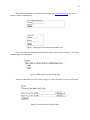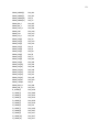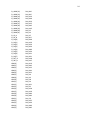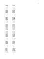
1
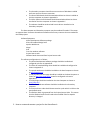
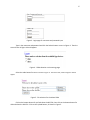
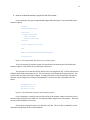
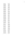
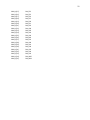
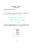
Remote FPGA Web Lab User Manual Robert Porter Olexiy Kovtunenko Mentor: Dr. Janusz Zalewski Florida Gulf Coast University, Ft. Myers, FL 33965-6565 03/30/2009 Quartus II Version 7.0 Build 33 SJ Web Edition Xilinx Spartan 3E Starter FPGA ISE Suite Web Edition 2 1. Introduction The purpose of this remote web lab is to have the user develop their VHDL code locally and then upload it to a website to see its operation on a real FPGA board via a webcam. The FPGA web lab assumes the user will have knowledge of VHDL and have their VHDL code before starting the operations outlined below. This project is meant to work concurrently with two different FPGA devices. These devices are different from each other, and therefore require different files to be operable. This document describes the steps to create and execute a successful project for the Altera FPGA and then the Xilinx FPGA. Each unique project will need a pin assignment file (See Appendix A), as well as the VHDL code supplied by the user. The Altera project needs file types VHD and QSF. The Xilinx project needs file types VHD and UCF. For both these projects, the filenames MUST be the same as the top level design name (excluding the filename extensions), for example: xorTest.ucf and xorTest.vhd CORRECT xor_timings.ucf and xorTest.vhd INCORRECT A high-level description of the development steps looks as follows: • The user should create their respective pin assignment file. • The user should navigate to the FPGA web page located at http://crackers/fpga/. This is only possible if the user is on the FGCU student network. • The user should select their respective pin assignment file and VHDL file. • The user should click the ‘upload’ button. • The web page should display a ‘wait for redirect’ and then redirect to the appropriate webcam page. • The web page should display the FPGA board with the executed VHDL code. In the following sections, we describe the equipment and software configuration with detailed steps to develop two examples; one for the Altera FPGA board and another for the Xilinx FPGA board. 2. Equipment and software configuration – Hardware Equipment: Altera Quartus 2 FPGA board Xilinx Spartan 3e FPGA board Webcam Host Computer Secondary Computer The hardware configuration is as follows: • The host computer should have some version of Windows installed and have an active internet connection. 3 • • • • The Secondary computer should have some version of Windows installed and have an active internet connection. The Altera FPGA board should be attached and have its drivers installed on the Host computer as shown in Appendix B. The Xilinx Spartan 3e FPGA board should be attached and have its drivers installed on the Host computer as shown in Appendix C. The webcam should be attached and have its drivers installed on the Secondary computer. The Host computer and Secondary computer may be combined if needed. The reason to separate them is because the webcam software utilizes many resources that are needed for the FPGA projects. Software Equipment: Altera Development Software package Xilinx ISE standard Design Suite Apache Web Server Mysql PHP Free Cam webcam software Project Source code Skeleton Batch Generated from Project Source code The software configuration is as follows: • The Altera Development Software package should be installed and configured as shown in Appendix B. • The Xilinx ISE standard Design Suite should be installed and configured as shown in Appendix C. • The apache web server should be installed on the Host Computer as shown at http://apache.org/. • The Mysql administration page should be installed on the Host Computer as shown at http://dev.mysql.com/. As well as configured as shown in Appendix D. • The PHP plugin should be installed on the Host Computer as shown at http://php.net/. • The Free Cam webcam software should be installed on the Secondary computer. • The Project Source code should be extracted to a path which is visible to the apache web server. • The Skeleton batch is generated from the Project Source Code. This means that the Skeleton batch file will need to be modified if the live Apache directory is changed. 3. How to create and execute a project for the Altera Board – 4 For this example a series of LEDs will display the word ‘Hello’. The actual VHDL code is shown in Figure. 1. LIBRARY ieee ; USE ieee.std_logic_1164.all ; ENTITY hello_world IS PORT ( A : IN STD_LOGIC ; b : OUT STD_LOGIC; c : OUT STD_LOGIC; d : OUT STD_LOGIC; e : OUT STD_LOGIC; f : OUT STD_LOGIC; g : OUT STD_LOGIC; h : OUT STD_LOGIC; i : OUT STD_LOGIC; j : OUT STD_LOGIC; k : OUT STD_LOGIC; l : OUT STD_LOGIC; m : OUT STD_LOGIC; n : OUT STD_LOGIC ); END hello_world ; ARCHITECTURE threeGates OF hello_world IS BEGIN b <= (NOT A); c <= (NOT A); d <= (NOT A); e <= (NOT A); f <= (NOT A); g <= (NOT A); h <= (NOT A); i <= (NOT A); j <= (NOT A); k <= (NOT A); l <= (NOT A); m <= (NOT A); n <= (NOT A); END threeGates; Figure 1 – The example VHDL code to be used in the Altera project. 5 The user should create a file named hello_world.vhd and type in the VHDL code found in Figure 1. The file should be saved to your Desktop for future use. The next step is to create the QSF file. A QSF file is the ‘pin assignment’ file. This file tells the Altera software which inputs and outputs to use. The pin locations can be found in Appendix A of this document. This appendix can be used if the program needs more inputs, outputs, or needs to know the names of said inputs and outputs. set_global_assignment -name DEVICE EP2C35F672C6 set_global_assignment -name FAMILY "Cyclone II" set_global_assignment -name ORIGINAL_QUARTUS_VERSION 7.0 set_global_assignment -name PROJECT_CREATION_TIME_DATE "20:45:32 MAY 01, 2008" set_global_assignment -name LAST_QUARTUS_VERSION 7.0 set_global_assignment -name TOP_LEVEL_ENTITY hello_world set_global_assignment -name VHDL_FILE hello_world.vhd set_instance_assignment -name PARTITION_HIERARCHY no_file_for_top_partition -to | -section_id Top set_global_assignment -name PARTITION_NETLIST_TYPE SOURCE -section_id Top set_location_assignment PIN_V2 -to A set_location_assignment PIN_L3 -to b set_location_assignment PIN_L6 -to c set_location_assignment PIN_P4 -to d set_location_assignment PIN_P3 -to e set_location_assignment PIN_T2 -to f set_location_assignment PIN_P6 -to g set_location_assignment PIN_P7 -to h set_location_assignment PIN_U9 -to i set_location_assignment PIN_U1 -to j set_location_assignment PIN_U2 -to k set_location_assignment PIN_W24 -to l set_location_assignment PIN_R3 -to m set_location_assignment PIN_T3 -to n set_global_assignment -name CYCLONEII_OPTIMIZATION_TECHNIQUE AREA set_global_assignment -name SOURCE_FILE hello_world.bdf Figure 2 – The example UCF code to be used in the Xilinx project. For this purpose, create a new file and name it hello_world.qsf. Please note that this is the same naming convention as the VHDL file. Then, type in the code shown in Figure 2. Save the file to your Desktop for future use. For this pin assignment file, Figure 2 should be used as a template. For other projects, lines that should be changed are any set_location_assignment or lines with ‘hello_world’ in them. At this point, the project consists of a VHD and a UCF file. This is all that is needed for correct execution and operation of the remote FPGA lab. Now the user should open a web browser and navigate to http://crackers/fpga. A screen shown in Figure 3 should appear. 6 Figure 3 - Login page for username and password input Type in the username and password and click the Submit button as seen in Figure 3. Then the screen shown in Figure 4 should appear. Figure 4 - FPGA selection on the settings page Select the radio button for Altera as shown in Figure 4. The next screen, shown in Figure 5 should appear. Figure 5 - File selection for the Altera FPGA Click on the browse button for qsf and select the QSF file, then click on the browse button for vhd and select the VHD file. Click on the Upload button, as shown in Figure 5. 7 Figure 6 - Webcam page after Altera execution After a maximum of around 5 minutes, the web page will refresh to show a webcam view. The compiled and executed VHDL code will be displayed on this page through the webcam, as demonstrated in Figure 6. Finally, when you are finished, click the Logout button, as indicated in the top left corner of Figure 6. 8 4. How to create and execute a project for the Xilinx board – For this example a xor gate is implemented using a LED and a switch. The actual VHDL code is shown in Figure A. library IEEE; use IEEE.STD_LOGIC_1164.ALL; entity xorTest is Port ( SW1 : in STD_LOGIC; SW2 : in STD_LOGIC; VAROUT : out STD_LOGIC); end xorTest; architecture LogicalFunction of xorTest is begin VAROUT <= (SW1 AND NOT SW2) OR (NOT SW1 AND SW2); end LogicalFunction; Figure A – The example VHDL code to be used in the Xilinx project. To run the example, first please create a file named xorTest.vhd and type in the VHDL code shown in Figure A. Save the file to your Desktop for future use. The next step is to create the UCF file, which is the ‘pins assignment’ file. This file tells the Xilinx software which inputs and outputs to use. The pin locations can be found on the physical board. This can be used if you need more inputs, outputs, or need to know the names of said inputs and outputs. However, the pin assignment is shown in the Appendix C, since the user will not be able to see the board. NET "VAROUT" LOC = "F9"; NET "SW1" LOC = "N17"; NET "SW2" LOC = "H18"; Figure B – The example UCF code to be used in the Xilinx project. For pin assignment, a new file name xorTest.ucf has to be created. Please note that this is the same naming convention as the VHDL file. The code provided in Figure B has to be typed in. Then save the file to your Desktop for future use. At this point, the project consists of a VHD and a UCF file. This is all that is needed for correct execution and operation of the remote FPGA lab. 9 Now, the user should open a web browser and navigate to http://crackers/fpga. The screen shown in Figure C should appear. Figure C - Login page for username and password input Type in the username and password and click the Login button as shown in Figure C. The screen shown in Figure D should appear. Figure D - FPGA selection on the settings page Select the radio button for Xilinx as shown in Figure D. A new screen shown in Figure E should appear. Figure E - File selection for the Xilinx FPGA 10 Now, click on the browse button for ucf and select the UCF file. Click on the browse button for vhd and select the VHD file. Then click on the Upload button as shown in Figure F. Figure F - Webcam page after Xilinx execution After a maximum of 5 around minutes, the web page will refresh to show a webcam view. The compiled and executed VHDL code will be displayed on this page through the webcam as illustrated in Figure F. Finally, when you are finished, click the Logout button, as show in the left upper corner of Figure F. 5. Conclusion – Accessibility: To make this project be realized fully, it will need to be accessed from outside the FGCU network. The main problem with this is the licensing for the Altera FPGA board. The Altera board uses what is called a ‘Floating License’. This license file is stored on the Onyx server at FGCU. Moving the license file to the local computer that the FPGA devices are attached to will fix this problem. Currently, to circumvent this, apache is set to run as a student account. This ensures access to the Onyx server on the student domain. JTAG Notes: Currently, the user is only able to view the uploaded code, but is not able to interact with the FPGA device. This means that any LEDs or sounds can be seen and heard through the webcam, but the user cannot press any buttons or flip any switches. To evolve the project, the user may be able to interact with a web page to modify the ‘bit file’ through the ‘JTAG chain’. The JTAG chain is the protocol that the computer and FPGA device use to communicate, whereas the bit file is the program loaded into the memory of the FPGA device. It is possible to prod through the JTAG protocol to modify the bit file and do things such as simulate pressing a button or flipping a switch. 11 There was very little research done on this topic so far, but it is known that this is possible and somewhat simple if managed through the Altera command line. More information and live help can be found by posting on the Altera forums at http://www.alteraforum.com/. Please note that there has not been any research done for modifying the bit file using the Xilinx board. However, all FPGA devices use a bit file and the JTAG protocol, so the theory should be similar. Visibility Notes: The current setup requires a webcam to be positioned above each FPGA device. In the project, there was only one webcam given, so the project members had to make do with that. The optimal way is to have each FPGA board enclosed in some sort of cardboard contraption. FPGA devices are best seen from a webcam when it is dark because they use bright LEDs. The problem with the current setup is that the webcam is hardly visible as shown in Figure 6 and Figure F. 12 Appendix A – Altera Board Pin Assignments This information was copied from the included CD-Rom for the Altera software. # Quartus II Version 5.1 Internal Build 160 09/19/2005 TO Full Version # File: D:\de2_pins\de2_pins.csv # Generated on: Wed Sep 28 09:40:34 2005 # Note: The column header names should not be changed if you wish to import this .csv file into the Quartus II software. To SW[0] SW[1] SW[2] SW[3] SW[4] SW[5] SW[6] SW[7] SW[8] SW[9] SW[10] SW[11] SW[12] SW[13] SW[14] SW[15] SW[16] SW[17] DRAM_ADDR[0] DRAM_ADDR[1] DRAM_ADDR[2] DRAM_ADDR[3] DRAM_ADDR[4] DRAM_ADDR[5] DRAM_ADDR[6] DRAM_ADDR[7] Location PIN_N25 PIN_N26 PIN_P25 PIN_AE14 PIN_AF14 PIN_AD13 PIN_AC13 PIN_C13 PIN_B13 PIN_A13 PIN_N1 PIN_P1 PIN_P2 PIN_T7 PIN_U3 PIN_U4 PIN_V1 PIN_V2 PIN_T6 PIN_V4 PIN_V3 PIN_W2 PIN_W1 PIN_U6 PIN_U7 PIN_U5 13 DRAM_ADDR[8] DRAM_ADDR[9] DRAM_ADDR[10] DRAM_ADDR[11] DRAM_BA_0 DRAM_BA_1 DRAM_CAS_N DRAM_CKE DRAM_CLK DRAM_CS_N DRAM_DQ[0] DRAM_DQ[1] DRAM_DQ[2] DRAM_DQ[3] DRAM_DQ[4] DRAM_DQ[5] DRAM_DQ[6] DRAM_DQ[7] DRAM_DQ[8] DRAM_DQ[9] DRAM_DQ[10] DRAM_DQ[11] DRAM_DQ[12] DRAM_DQ[13] DRAM_DQ[14] DRAM_DQ[15] DRAM_LDQM DRAM_UDQM DRAM_RAS_N DRAM_WE_N FL_ADDR[0] FL_ADDR[1] FL_ADDR[2] FL_ADDR[3] FL_ADDR[4] FL_ADDR[5] FL_ADDR[6] FL_ADDR[7] FL_ADDR[8] FL_ADDR[9] FL_ADDR[10] FL_ADDR[11] PIN_W4 PIN_W3 PIN_Y1 PIN_V5 PIN_AE2 PIN_AE3 PIN_AB3 PIN_AA6 PIN_AA7 PIN_AC3 PIN_V6 PIN_AA2 PIN_AA1 PIN_Y3 PIN_Y4 PIN_R8 PIN_T8 PIN_V7 PIN_W6 PIN_AB2 PIN_AB1 PIN_AA4 PIN_AA3 PIN_AC2 PIN_AC1 PIN_AA5 PIN_AD2 PIN_Y5 PIN_AB4 PIN_AD3 PIN_AC18 PIN_AB18 PIN_AE19 PIN_AF19 PIN_AE18 PIN_AF18 PIN_Y16 PIN_AA16 PIN_AD17 PIN_AC17 PIN_AE17 PIN_AF17 14 FL_ADDR[12] FL_ADDR[13] FL_ADDR[14] FL_ADDR[15] FL_ADDR[16] FL_ADDR[17] FL_ADDR[18] FL_ADDR[19] FL_ADDR[20] FL_ADDR[21] FL_CE_N FL_OE_N FL_DQ[0] FL_DQ[1] FL_DQ[2] FL_DQ[3] FL_DQ[4] FL_DQ[5] FL_DQ[6] FL_DQ[7] FL_RST_N FL_WE_N HEX0[0] HEX0[1] HEX0[2] HEX0[3] HEX0[4] HEX0[5] HEX0[6] HEX1[0] HEX1[1] HEX1[2] HEX1[3] HEX1[4] HEX1[5] HEX1[6] HEX2[0] HEX2[1] HEX2[2] HEX2[3] HEX2[4] HEX2[5] PIN_W16 PIN_W15 PIN_AC16 PIN_AD16 PIN_AE16 PIN_AC15 PIN_AB15 PIN_AA15 PIN_Y15 PIN_Y14 PIN_V17 PIN_W17 PIN_AD19 PIN_AC19 PIN_AF20 PIN_AE20 PIN_AB20 PIN_AC20 PIN_AF21 PIN_AE21 PIN_AA18 PIN_AA17 PIN_AF10 PIN_AB12 PIN_AC12 PIN_AD11 PIN_AE11 PIN_V14 PIN_V13 PIN_V20 PIN_V21 PIN_W21 PIN_Y22 PIN_AA24 PIN_AA23 PIN_AB24 PIN_AB23 PIN_V22 PIN_AC25 PIN_AC26 PIN_AB26 PIN_AB25 15 HEX2[6] HEX3[0] HEX3[1] HEX3[2] HEX3[3] HEX3[4] HEX3[5] HEX3[6] HEX4[0] HEX4[1] HEX4[2] HEX4[3] HEX4[4] HEX4[5] HEX4[6] HEX5[0] HEX5[1] HEX5[2] HEX5[3] HEX5[4] HEX5[5] HEX5[6] HEX6[0] HEX6[1] HEX6[2] HEX6[3] HEX6[4] HEX6[5] HEX6[6] HEX7[0] HEX7[1] HEX7[2] HEX7[3] HEX7[4] HEX7[5] HEX7[6] KEY[0] KEY[1] KEY[2] KEY[3] LEDR[0] LEDR[1] PIN_Y24 PIN_Y23 PIN_AA25 PIN_AA26 PIN_Y26 PIN_Y25 PIN_U22 PIN_W24 PIN_U9 PIN_U1 PIN_U2 PIN_T4 PIN_R7 PIN_R6 PIN_T3 PIN_T2 PIN_P6 PIN_P7 PIN_T9 PIN_R5 PIN_R4 PIN_R3 PIN_R2 PIN_P4 PIN_P3 PIN_M2 PIN_M3 PIN_M5 PIN_M4 PIN_L3 PIN_L2 PIN_L9 PIN_L6 PIN_L7 PIN_P9 PIN_N9 PIN_G26 PIN_N23 PIN_P23 PIN_W26 PIN_AE23 PIN_AF23 16 LEDR[2] LEDR[3] LEDR[4] LEDR[5] LEDR[6] LEDR[7] LEDR[8] LEDR[9] LEDR[10] LEDR[11] LEDR[12] LEDR[13] LEDR[14] LEDR[15] LEDR[16] LEDR[17] LEDG[0] LEDG[1] LEDG[2] LEDG[3] LEDG[4] LEDG[5] LEDG[6] LEDG[7] LEDG[8] CLOCK_27 CLOCK_50 EXT_CLOCK PS2_CLK PS2_DAT UART_RXD UART_TXD LCD_RW LCD_EN LCD_RS LCD_DATA[0] LCD_DATA[1] LCD_DATA[2] LCD_DATA[3] LCD_DATA[4] LCD_DATA[5] LCD_DATA[6] PIN_AB21 PIN_AC22 PIN_AD22 PIN_AD23 PIN_AD21 PIN_AC21 PIN_AA14 PIN_Y13 PIN_AA13 PIN_AC14 PIN_AD15 PIN_AE15 PIN_AF13 PIN_AE13 PIN_AE12 PIN_AD12 PIN_AE22 PIN_AF22 PIN_W19 PIN_V18 PIN_U18 PIN_U17 PIN_AA20 PIN_Y18 PIN_Y12 PIN_D13 PIN_N2 PIN_P26 PIN_D26 PIN_C24 PIN_C25 PIN_B25 PIN_K4 PIN_K3 PIN_K1 PIN_J1 PIN_J2 PIN_H1 PIN_H2 PIN_J4 PIN_J3 PIN_H4 17 LCD_DATA[7] LCD_ON LCD_BLON SRAM_ADDR[0] SRAM_ADDR[1] SRAM_ADDR[2] SRAM_ADDR[3] SRAM_ADDR[4] SRAM_ADDR[5] SRAM_ADDR[6] SRAM_ADDR[7] SRAM_ADDR[8] SRAM_ADDR[9] SRAM_ADDR[10] SRAM_ADDR[11] SRAM_ADDR[12] SRAM_ADDR[13] SRAM_ADDR[14] SRAM_ADDR[15] SRAM_ADDR[16] SRAM_ADDR[17] SRAM_DQ[0] SRAM_DQ[1] SRAM_DQ[2] SRAM_DQ[3] SRAM_DQ[4] SRAM_DQ[5] SRAM_DQ[6] SRAM_DQ[7] SRAM_DQ[8] SRAM_DQ[9] SRAM_DQ[10] SRAM_DQ[11] SRAM_DQ[12] SRAM_DQ[13] SRAM_DQ[14] SRAM_DQ[15] SRAM_WE_N SRAM_OE_N SRAM_UB_N SRAM_LB_N SRAM_CE_N PIN_H3 PIN_L4 PIN_K2 PIN_AE4 PIN_AF4 PIN_AC5 PIN_AC6 PIN_AD4 PIN_AD5 PIN_AE5 PIN_AF5 PIN_AD6 PIN_AD7 PIN_V10 PIN_V9 PIN_AC7 PIN_W8 PIN_W10 PIN_Y10 PIN_AB8 PIN_AC8 PIN_AD8 PIN_AE6 PIN_AF6 PIN_AA9 PIN_AA10 PIN_AB10 PIN_AA11 PIN_Y11 PIN_AE7 PIN_AF7 PIN_AE8 PIN_AF8 PIN_W11 PIN_W12 PIN_AC9 PIN_AC10 PIN_AE10 PIN_AD10 PIN_AF9 PIN_AE9 PIN_AC11 18 OTG_ADDR[0] OTG_ADDR[1] OTG_CS_N OTG_RD_N OTG_WR_N OTG_RST_N OTG_DATA[0] OTG_DATA[1] OTG_DATA[2] OTG_DATA[3] OTG_DATA[4] OTG_DATA[5] OTG_DATA[6] OTG_DATA[7] OTG_DATA[8] OTG_DATA[9] OTG_DATA[10] OTG_DATA[11] OTG_DATA[12] OTG_DATA[13] OTG_DATA[14] OTG_DATA[15] OTG_INT0 OTG_INT1 OTG_DACK0_N OTG_DACK1_N OTG_DREQ0 OTG_DREQ1 OTG_FSPEED OTG_LSPEED TDI TCS TCK TDO TD_RESET VGA_R[0] VGA_R[1] VGA_R[2] VGA_R[3] VGA_R[4] VGA_R[5] VGA_R[6] PIN_K7 PIN_F2 PIN_F1 PIN_G2 PIN_G1 PIN_G5 PIN_F4 PIN_D2 PIN_D1 PIN_F7 PIN_J5 PIN_J8 PIN_J7 PIN_H6 PIN_E2 PIN_E1 PIN_K6 PIN_K5 PIN_G4 PIN_G3 PIN_J6 PIN_K8 PIN_B3 PIN_C3 PIN_C2 PIN_B2 PIN_F6 PIN_E5 PIN_F3 PIN_G6 PIN_B14 PIN_A14 PIN_D14 PIN_F14 PIN_C4 PIN_C8 PIN_F10 PIN_G10 PIN_D9 PIN_C9 PIN_A8 PIN_H11 19 VGA_R[7] VGA_R[8] VGA_R[9] VGA_G[0] VGA_G[1] VGA_G[2] VGA_G[3] VGA_G[4] VGA_G[5] VGA_G[6] VGA_G[7] VGA_G[8] VGA_G[9] VGA_B[0] VGA_B[1] VGA_B[2] VGA_B[3] VGA_B[4] VGA_B[5] VGA_B[6] VGA_B[7] VGA_B[8] VGA_B[9] VGA_CLK VGA_BLANK VGA_HS VGA_VS VGA_SYNC I2C_SCLK I2C_SDAT TD_DATA[0] TD_DATA[1] TD_DATA[2] TD_DATA[3] TD_DATA[4] TD_DATA[5] TD_DATA[6] TD_DATA[7] TD_HS TD_VS AUD_ADCLRCK AUD_ADCDAT PIN_H12 PIN_F11 PIN_E10 PIN_B9 PIN_A9 PIN_C10 PIN_D10 PIN_B10 PIN_A10 PIN_G11 PIN_D11 PIN_E12 PIN_D12 PIN_J13 PIN_J14 PIN_F12 PIN_G12 PIN_J10 PIN_J11 PIN_C11 PIN_B11 PIN_C12 PIN_B12 PIN_B8 PIN_D6 PIN_A7 PIN_D8 PIN_B7 PIN_A6 PIN_B6 PIN_J9 PIN_E8 PIN_H8 PIN_H10 PIN_G9 PIN_F9 PIN_D7 PIN_C7 PIN_D5 PIN_K9 PIN_C5 PIN_B5 20 AUD_DACLRCK AUD_DACDAT AUD_XCK AUD_BCLK ENET_DATA[0] ENET_DATA[1] ENET_DATA[2] ENET_DATA[3] ENET_DATA[4] ENET_DATA[5] ENET_DATA[6] ENET_DATA[7] ENET_DATA[8] ENET_DATA[9] ENET_DATA[10] ENET_DATA[11] ENET_DATA[12] ENET_DATA[13] ENET_DATA[14] ENET_DATA[15] ENET_CLK ENET_CMD ENET_CS_N ENET_INT ENET_RD_N ENET_WR_N ENET_RST_N IRDA_TXD IRDA_RXD SD_DAT SD_DAT3 SD_CMD SD_CLK GPIO_0[0] GPIO_0[1] GPIO_0[2] GPIO_0[3] GPIO_0[4] GPIO_0[5] GPIO_0[6] GPIO_0[7] GPIO_0[8] PIN_C6 PIN_A4 PIN_A5 PIN_B4 PIN_D17 PIN_C17 PIN_B18 PIN_A18 PIN_B17 PIN_A17 PIN_B16 PIN_B15 PIN_B20 PIN_A20 PIN_C19 PIN_D19 PIN_B19 PIN_A19 PIN_E18 PIN_D18 PIN_B24 PIN_A21 PIN_A23 PIN_B21 PIN_A22 PIN_B22 PIN_B23 PIN_AE24 PIN_AE25 PIN_AD24 PIN_AC23 PIN_Y21 PIN_AD25 PIN_D25 PIN_J22 PIN_E26 PIN_E25 PIN_F24 PIN_F23 PIN_J21 PIN_J20 PIN_F25 21 GPIO_0[9] GPIO_0[10] GPIO_0[11] GPIO_0[12] GPIO_0[13] GPIO_0[14] GPIO_0[15] GPIO_0[16] GPIO_0[17] GPIO_0[18] GPIO_0[19] GPIO_0[20] GPIO_0[21] GPIO_0[22] GPIO_0[23] GPIO_0[24] GPIO_0[25] GPIO_0[26] GPIO_0[27] GPIO_0[28] GPIO_0[29] GPIO_0[30] GPIO_0[31] GPIO_0[32] GPIO_0[33] GPIO_0[34] GPIO_0[35] GPIO_1[0] GPIO_1[1] GPIO_1[2] GPIO_1[3] GPIO_1[4] GPIO_1[5] GPIO_1[6] GPIO_1[7] GPIO_1[8] GPIO_1[9] GPIO_1[10] GPIO_1[11] GPIO_1[12] GPIO_1[13] GPIO_1[14] PIN_F26 PIN_N18 PIN_P18 PIN_G23 PIN_G24 PIN_K22 PIN_G25 PIN_H23 PIN_H24 PIN_J23 PIN_J24 PIN_H25 PIN_H26 PIN_H19 PIN_K18 PIN_K19 PIN_K21 PIN_K23 PIN_K24 PIN_L21 PIN_L20 PIN_J25 PIN_J26 PIN_L23 PIN_L24 PIN_L25 PIN_L19 PIN_K25 PIN_K26 PIN_M22 PIN_M23 PIN_M19 PIN_M20 PIN_N20 PIN_M21 PIN_M24 PIN_M25 PIN_N24 PIN_P24 PIN_R25 PIN_R24 PIN_R20 22 GPIO_1[15] GPIO_1[16] GPIO_1[17] GPIO_1[18] GPIO_1[19] GPIO_1[20] GPIO_1[21] GPIO_1[22] GPIO_1[23] GPIO_1[24] GPIO_1[25] GPIO_1[26] GPIO_1[27] GPIO_1[28] GPIO_1[29] GPIO_1[30] GPIO_1[31] GPIO_1[32] GPIO_1[33] GPIO_1[34] GPIO_1[35] PIN_T22 PIN_T23 PIN_T24 PIN_T25 PIN_T18 PIN_T21 PIN_T20 PIN_U26 PIN_U25 PIN_U23 PIN_U24 PIN_R19 PIN_T19 PIN_U20 PIN_U21 PIN_V26 PIN_V25 PIN_V24 PIN_V23 PIN_W25 PIN_W23 23 Appendix B – Excerpt from the Altera FPGA Setup Manual. Please follow these instructions to correctly install the Altera web suite on the Host Compter. The device driver is located on the FPGA_WEBSITE folder located on the desktop of the host computer. Software Installation: To install the Quartus II Software, insert the Altera Quartus II installation CD into your CD-Rom. An installation window will open prompting you to install the Professional edition or the Free Edition. Select the Free edition and wait for the installation to finish. On slower machines it can take up to an hour to finish. While that is installing, the license file can be obtained by going to the www.altera.com website and requesting a license. The correct page is hard to find, so the direct link is: https://www.altera.com/support/licensing/free_software/lic-q2web.jsp Sign up to this website by creating a new account. After logging in, fill out the information on this form such as Name, location and telephone number. The registration information section requires the MAC address of the computer that has the Quartus II software installed. To do this, open command prompt and type ‘ipconfig /all’. Here the MAC address can be found. 24 On the next page, fill out the selections that best suit the purpose that the Altera Software will be used for (mainly Academic). If the license key doesn’t come to the e-mail provided in 10 minutes or so, it probably means the key will not be coming. If this is the case, fill out the information again and a key will be eventually sent. Once the key (in .dat format) has been successfully sent through email, save the file to some location such as the ‘My Documents’ folder. Open the Quartus II 7.0 Web Edition. Click Specify License file and open the .dat located in the folder you saved it to. Hardware Installation: Now that the software has been installed it has to recognize the device correctly. Plug in the DE-2 board through USB into the computer. Power does not need to be on at this point. The normal window for installing hardware should open. Click ‘install this software from a specified location’. The driver for this DE-2 board is located on your drive. If you did not change the default path for the software installation, the driver should be located at: C:\altera\70\quartus\drivers\usb-blaster\x32 (vista users have the x64 folder). Section Experiments Description After hardware and software have been setup properly, the first experiment we conducted was an experiment with Altera given software for simple I/O manipulation. After simple testing was successfully conducted we were assured in our correct setup of host computer and device, due to this step we excluded possibility of setup failure; therefore if we run into further problems with execution, they are probably due to our faulty design or errors within VHDL code. Experiment 1: Switches in different position give 1. Purpose: I/O manipulations and VHDL practice. The logic of the experiment can be described as follows. 25 The code can be seen bellow: LIBRARY ieee; USE ieee.std_logic_1164.all; ENTITY light IS PORT ( x1, x2 : IN STD_LOGIC ; f : OUT STD_LOGIC ) ; END light; ARCHITECTURE LogicFunction OF light IS BEGIN f <= (x1 AND NOT x2) OR (NOT x1 AND x2); END LogicFunction ; Where X1 and X2 are inputs and F is the output. X1 and X2 were assigned to Switch 0 (SW0) and Switch 1 (SW1) accordingly. The output F was assigned to Green Led 0 (LEDG0). Meaning that when either SW0 or SW1 switched to ON, sending input of 1 into the circuit and causing output to become 1, the LEDG0 would light with green light. Experiment 2: 3 bit digit display using 7 light digital display. Purpose: 7 light digital display manipulation and Boolean algebra practice. 26 The lights on digital display are ON by default, therefore when according output is 0 (FALSE) the light stays on, but when its 1 (TRUE) the light goes off. Since we are using 3 bit input the maximum number we can display is 7. For example in digital display the top light is used in displaying following digits: 0(000), 2(010), 3(011), 5(101), 6(110), 7(111). Not used to display 1(001) and 4(100) therefore the output F can be described as follows: F <= NOT((A’B’C) + (AB’C’)) Using same logic following can be calculated for all seven light, then program in VHDL. Note in following code bellow for simplicity of input we reverted bits, meaning that smallest (20) is on the left so 1 is 100 as oppose to traditional 001. The code can be found bellow. LIBRARY ieee ; USE ieee.std_logic_1164.all ; ENTITY ledTest IS PORT ( A : IN STD_LOGIC ; B : IN STD_LOGIC ; C : IN STD_LOGIC ; d : OUT STD_LOGIC; e : OUT STD_LOGIC; f : OUT STD_LOGIC; g : OUT STD_LOGIC; h : OUT STD_LOGIC; i : OUT STD_LOGIC 27 j : OUT STD_LOGIC ) ; END ledTest ; ARCHITECTURE threeGates OF ledTest IS BEGIN --for LED0 --AB'C' + A'B'C d <= (A AND NOT B AND NOT C) OR (NOT A AND NOT B AND C); --for LED1 --AB'C + A'BC e <= (A AND NOT B AND C) OR (NOT A AND B AND C); --for LED2 --A'BC' F <= (NOT A AND B AND NOT C); --for LED3 --AB'C' + A'B'C + ABC g <= (A AND NOT B AND NOT C) OR (NOT A AND NOT B AND C) OR (A AND B AND C); --for LED4 --AB'C' + ABC' + A'B'C + AC h <= (A AND NOT B AND NOT C) OR (A AND B AND NOT C) OR (NOT A AND NOT B AND C) OR (A AND C); --for LED5 --AB'C' + A'BC' + AB i <= (A AND NOT B AND NOT C) OR (NOT A AND B AND NOT C) OR (A AND B); --for LED6 28 --B'C' + ABC j <= (NOT B AND NOT C) OR (A AND B AND C); END threeGates; Experiment was successful and output was received according to logic described above. Experimental setup The setup was similar for both projects, therefore both experiment above will have one setup description. Hardware setup: 1) Host Computer with available USB ports, appropriate drivers and Qaurtus II 7.0 Web Edition software setup. 2) Altera DE2 Development and Educational Board. 3) USB wire. 4) Native Altera power supply for Altera DE2 board. Host computer connected to Altera DE2 board via USB cable. Software Setup: To start working on a new design we first have to define a new design project. Quartus II software makes the designer’s task easy by providing support in the form of a wizard. Create a new project as follows: 1) Select File > New Project Wizard, which indicates the capability of this. Press Next to get to the next window. 2) Set the working directory. The project must have a name, which is usually the same as the toplevel design entity that will be included in the project (in your VHDL code: ENTITY Project_Name IS …). Choose same name for both the project and the top-level entity. Press Next. Since we 29 have not yet created the directory for the project, Quartus II software displays the pop-up box asking if it should create the desired directory. Click Yes. 3) The wizard makes it easy to specify which existing files (if any) should be included in the project. Since we do not have any existing files, click Next. 4) We have to specify the type of device in which the designed circuit will be implemented. Choose Cyclone TM II as the target device family. We can let Quartus II software select a specific device in the family, or we can choose the device explicitly. We will take the latter approach. From the list of available devices, choose the device called EP2C35F672C6 which is the FPGA used on Altera’s DE2 board. Press Next. 5) The user can specify any third-party tools that should be used. A commonly used term for CAD software for electronic circuits is EDA tools, where the acronym stands for Electronic Design Automation. This term is used in Quartus II messages that refer to third-party tools, which are the tools developed and marketed by companies other than Altera. Since we will rely solely on Quartus II tools, we will not choose any other tools. Press Next. 6) Press Finish, which returns to the main Quartus II window, but with project specified as the new project, in the display title bar. 7) Select File > New choose VHDL File, and click OK. This opens the Text Editor window. The first step is to specify a name for the file that will be created. Select File > Save As to open the popup box. In the box labeled Save as type choose VHDL File. In the box labeled File name type same name as a projects name and the top-level entity of your VHDL code (ENTITY Top_Level 30 IS…). Put a checkmark in the box Add file to current project. Click Save, which puts the file into the project directory and leads to the Text Editor window. Maximize the Text Editor window and enter the VHDL code. Save the file by typing File > Save, or by typing the shortcut Ctrl-s. 8) Run the Compiler by selecting Processing > Start Compilation, or by clicking on the toolbar icon that looks like a purple triangle. As the compilation moves through various stages, its progress is reported in a window on the left side of the Quartus II display. Successful (or unsuccessful) compilation is indicated in a pop-up box. Acknowledge it by clicking OK, which leads to the Quartus II display the message window, at the bottom of the figure, various messages are displayed. In case of errors, there will be appropriate messages given. When the compilation is finished, a compilation report is produced. A window showing this report is opened automatically. 9) During the compilation above, the Quartus II Compiler was free to choose any pins on the selected FPGA to serve as inputs and outputs. However, the DE2 board has hardwired connections between the FPGA pins and the other components on the board. We will use two toggle switches, labeled SW0 and SW1, to provide the external inputs, x1 and x2, to our example circuit. These switches are connected to the FPGA pins N25 and N26, respectively. We will connect the output f to the green light-emitting diode labeled LEDG0, which is hardwired to the FPGA pin AE22. Pin assignments are made by using the Assignment Editor. Select Assignments > Pins to reach the window. Then open up the Assingnment Editor by going to Assignments>Assignment Editor. In the assignment editor Under Category select Pin. Double-click on the entry <<new>> which is highlighted in blue in the column labeled To. The drop-down menu will appear. Click on x1 as 31 the first pin to be assigned; this will enter x1 in the displayed table. Follow this by doubleclicking on the box to the right of this new x1 entry, in the column labeled Location. Now, the new drop-down menu will appear. Scroll down and select PIN_N25. Instead of scrolling down the menu to find the desired pin, you can just type the name of the pin (N25) in the Location box. Use the same procedure to assign input x2 to pin N26 and output f to pin AE22, which is a result. Choose File > Save to save assignments that were made. Recompile your project by going to Processing > Start Compilation. 10) Now we are ready to run the project on the board. Flip the RUN/PROG switch into the RUN position. Select Tools > Programmer to reach the run setup window. Here it is necessary to specify the programming hardware and the mode that should be used. If not already chosen by default, select JTAG in the Mode box. Also, if the USB-Blaster is not chosen by default, press the Hardware Setup... button and select the USB-Blaster in the window that pops up. Make sure that Program/Configure checkbox is clicked for the FileName.sof. Then click on start. The usually blinking of lights and Welcome message on LCD screen will disappear and only blue lights indicating power and ready will remain lit, now you know that your circuit is loaded into the board and ready for the execution. 11) Test your circuits by switching assigned toggle switched on and off and see if yielded result appears on the assigned LED light. Results Experiment 1: when toggle lights were switched accordingly, expected light lit, indicating the success of designed circuit. 32 Experiment 2: we were able to successfully display digits 0-7, using 3 toggle switches as 3 bit input and 7 light HEX output. Appendix C – Links to install and setup the Xilinx ISE suite Download the Xilinx ISE version 10.1 from the Xilinx website: http://www.xilinx.com/support/download/index.htm. The device driver is located on the Desktop of the host computer (http://crackers). Appendix D - Mysql configuration The FPGA project uses two tables within a single database. The database should have the following. • • • The root username should be root, the root password should be fpga. A table should be created named `fpgainfo`; There should be two fields which should be `fpga` = altera, Xilinx VarChar(20) and `name` = “”,”” VarChar(20). A table should be created named `userinfo`; There should be 3 fields which should be `username`= VarChar(20), `password`=MD5() VarChar(20), and `admin`= 0 or 1 (1 for administrator and 0 for regular user) INT(). A useful tool for database administration is called phpmyadmin found from http://www.phpmyadmin.net/home_page/index.php. A copy of phpmyadmin with the working database can be found at http://crackers/phpmyadmin/index.php. Please note that phpmyadmin will only work after PHP has been installed on the Host Computer.