1
Freescale Semiconductor, Inc.
Programming Model
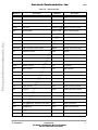
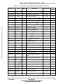
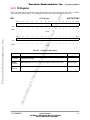
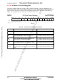
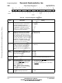
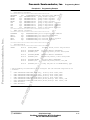
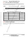
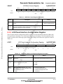
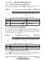
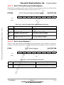
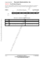
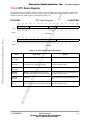
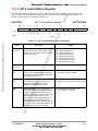
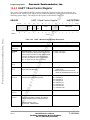
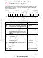
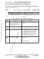
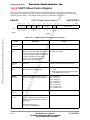
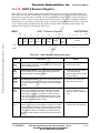
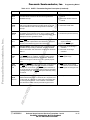
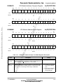
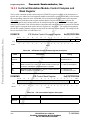
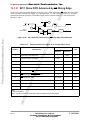
14.4.12 UART 2 Miscellaneous Register
UMISC2
BIT
15
14
13
12
11
10
BA
UD
TES
T
CLK
SR
C
FOR
CE
PER
R
LO
OP
BAU
D
RES
ET
IR
TES
T
rw
rw
rw
rw
rw
rw
0
0
0
0
0
0
9
8
0
0x(FF)FFF918
7
6
5
4
3
2
RTS
2
CO
NT
RT
S2
IR
DA
EN
IRD
A
LO
OP
RX
PO
L
TX
PO
L
rw
rw
rw
rw
rw
rw
0
0
0
0
0
0
0
1
BIT
0
0
0
0x0000
DU
RESET
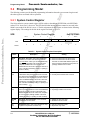
UART 2 Miscellaneous Register
Description
MIC
Name
ON
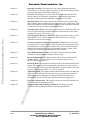
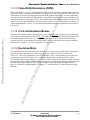
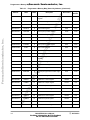
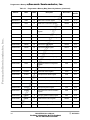
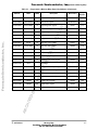
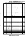
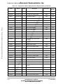
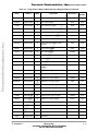
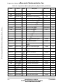
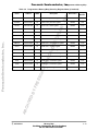
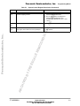
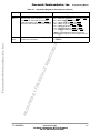
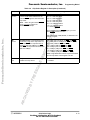
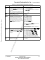
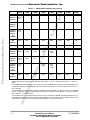
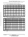
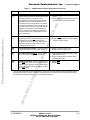
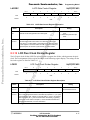
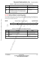
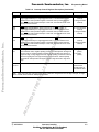
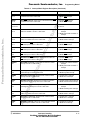
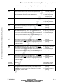
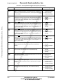
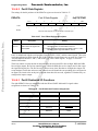
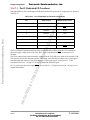
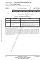
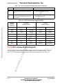
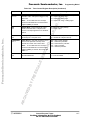
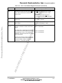
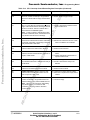
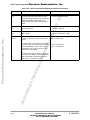
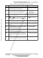
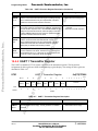
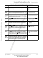
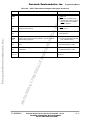
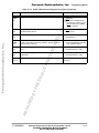
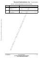
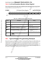
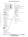
Table 14-14. UART 2 Miscellaneous Register Description
Setting
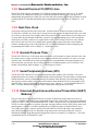
Baud Rate Generator Testing—This bit puts the baud rate
generator in test mode. The integer and non-integer prescalers, as well as the divider, are broken into 4-bit nibbles for testing. This bit should remain 0 for normal operation.
0 = Normal mode.
1 = Test mode.
CLKSRC
Bit 14
Clock Source—This bit selects the source of the 1x bit clock
for transmission and reception. When this bit is high, the bit
clock is derived directly from the UCLK pin (it must be configured as an input). When it is low (normal), the bit clock is supplied by the baud rate generator. This bit allows high-speed
synchronous applications, in which a clock is provided by the
external system.
0 = Bit clock is generated by the
baud rate generator.
1 = Bit clock is supplied by the
UCLK pin.
FORCE
PERR
Bit 13
Force Parity Error—When this bit is high, it forces the transmitter to generate parity errors, if parity is enabled. This bit is
for system debugging.
0 = Generate normal parity.
1 = Generate inverted parity (error).
LOOP
Bit 12
Loopback—This bit controls loopback for system testing purposes. When this bit is high, the receiver input is internally connected to the transmitter and ignores the RXD2 pin. The TXD2
pin is unaffected by this bit.
0 = Normal receiver operation.
1 = Internally connects the
transmitter output to the
receiver input.
BAUD
RESET
Bit 11
Baud Rate Generator Reset—This bit resets the baud rate
generator counters.
0 = Normal operation.
1 = Reset baud counters.
IRTEST
Bit 10
Infrared Testing—This bit connects the output of the IrDA circuitry to the TXD2 pin. This provides test visibility to the IrDA
module.
0 = Normal operation.
1 = IrDA test mode.
Reserved
Bits 9–8
Reserved
These bits are reserved and should
be set to 0.
14-26
CH
IVE
DB
YF
RE
ES
CA
LE
SE
BAUD
TEST
Bit 15
AR
Freescale Semiconductor, Inc...
TYPE
CT
OR
, IN
C.
200
5
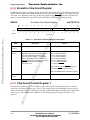
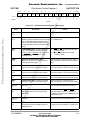
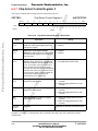
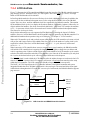
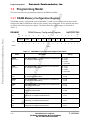
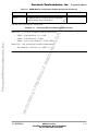
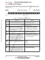
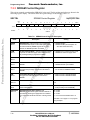
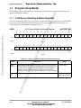
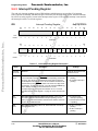
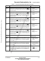
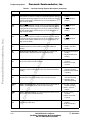
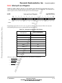
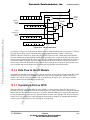
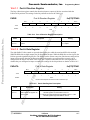
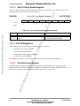
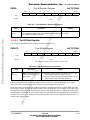
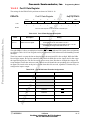
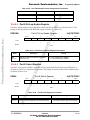
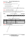
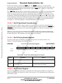
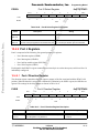
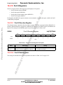
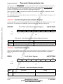
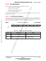
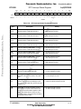
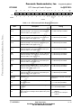
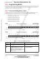
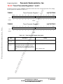
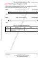
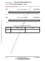
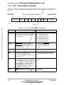
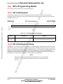
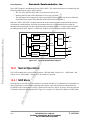
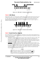
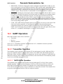
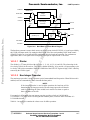
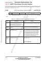
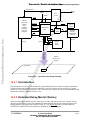
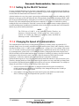
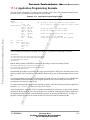
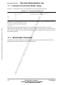
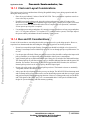
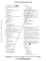
The UART 2 miscellaneous (UMISC2) register contains miscellaneous bits to control test features of the
UART 2 module. Some bits, however, are only used for factory testing and should not be used. The bit
position assignments for this register are shown in the following register display. The settings for this
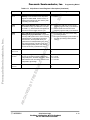
register are described in Table 14-14.
MC68VZ328 User’s Manual
For More Information On This Product,
Go to: www.freescale.com