1
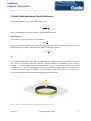
.....................OFET......OLED......OPV......Substrates......Components......Materials..................... OFET measurement manual: Probe Station (E451) Low Density OFET Test Board (E222) High Density OFET Test Board (E481) Ossila Ltd Copyright © 2009 – 2014 1 enabling organic electronics Contents Safety Standards Statement Declaration of Conformity 3 4 Probe Station Overview Technical Data OFET Measurement 4-point Probe Equations: Sheet Resistance Mobility Maintenance 6 9 11 13 14 17 18 Low Density OFET Test Board Overview Technical Data OFET Measurement 19 20 22 High Density OFET Test Board Overview Technical Data OFET Measurement 24 25 27 Measurement Error and Noise High Accuracy Measurement 29 30 Ossila Ltd Copyright © 2009 – 2014 2 enabling organic electronics Safety Warning To avoid safety hazards obey the following: Do not leave devices with applied bias or current unattended as a power failure may result in board damage or device damage and potentially hazardous situations. The maximum allowed driving voltage is ± 100 V and the maximum current is ±100 mA. Operating the probe station or OFET test board outside the operational range can cause damage to the device and greatly increase the risk of electrical shock. The electrical components under high voltage are exposed. The user must therefore exert extreme caution when operating the probe station and maintain a safety distance of at least 1 m during high voltage operations. Do not operate the switches or touch the probe station or OFET test board when voltage and/or current are applied. Caution To avoid damaging devices or equipment obey the following: Avoid electrostatic discharge (ESD) as this may damage the device. To avoid damage, use static discharge and prevention equipment where necessary. Only use the device for the purposes intended (described in this document) Do not expose the device to any inappropriate cleaning fluids or solvents. Follow good practice when setting up the test system. Avoid placing mobile phones on top of the system as this can cause interference. Ossila Ltd Copyright © 2009 – 2014 3 enabling organic electronics EC Declaration of Conformity In line with directive 2004/108/EC of the European Parliament and of the Council and directive 2006/95/EC of the European Parliament and of the Council. -Manufacturer Name: Ossila Limited Manufacturer Address: Kroto Innovation Centre, North Campus, Broad Lane, Sheffield, S3 7HQ -Item: OFET Probe Station, Low Density OFET Test Board, High Density OFET Test Board Model number: E451/E222/E481 -Specifications of product under harmonised standards: 2004/108/EC EN 61326-1:2006 Electrical equipment for measurement, control and laboratory use – EMC requirements – Part 1: General requirements IEC 61326-1:2005 EN 61326-2-1:2006 Electrical equipment for measurement, control and laboratory use – EMC requirements – Part 2-1: Particular requirements – Test configurations, operational conditions and performance criteria for sensitive test and measurement equipment for EMC unprotected applications IEC 61326-2-1:2005 2006/95/EC EN 61010-1:2010 Safety requirements for electrical equipment for measurement, control, and laboratory use - Part 1: General requirements IEC 61010-1:2010 EN 61010-2-030:2010 Safety requirements for electrical equipment for measurement, control, and laboratory use - Part 2-030: Particular requirements for testing and measuring circuits IEC 61010-2-030:2010 EN 61140:2002 Protection against electric shock - Common aspects for installation and equipment IEC 61140:2001 EN 61187:1994 Electrical and electronic measuring equipment - Documentation IEC 61187:1993 (Modified) Ossila Ltd Copyright © 2009 – 2014 4 enabling organic electronics EN 61010-2-081:2002 Safety requirements for electrical equipment for measurement, control and laboratory use - Part 2-081: Particular requirements for automatic and semiautomatic laboratory equipment for analysis and other purposes IEC 61010-2-081:2001 Declaration: I hereby declare that the equipment named above has been designed to comply with the relevant sections of the above referenced specifications. The unit complies with all applicable Essential Requirements of the Directives. -Signed: Name: Dr James Kingsley Date: 07/05/2014 Ossila Ltd Copyright © 2009 – 2014 5 enabling organic electronics Probe Station Overview The optic probe station allows for quick and easy testing of individual substrates on a variety of OFET electrode designs thanks to the interchangeable probe board. The unit is composed of two main sections, the XYZ position stages and the low-noise probe board. The positioning stage is controlled through three micrometer screws (0.5 mm accuracy) and can be easily operated in a glove box. The substrate is loaded in to the substrate holder, mounted on top of the vertical stage, and is kept firmly in position by a steel bar acting as top gate pad contact. The bottom and the edge of the holder provide an alternative route to electrically connect the gate to the SMU. The probe itself uses POGO© connectors which are rounded and spring loaded to allow robust, non-destructive electrical connection with the electrode of the Device Under Test (DUT). Note The probe station has been tested to allow for non-destructive contact in case of metal/adhesion layer electrodes only (Au/Cr, Pt/Ti etc). Metal with poor adhesion properties on silicon or glass, such as Au, are prone to be damaged by the POGO© unless extreme care is taken during the positioning of the probe on the electrodes. The test board has a double ground plane acting as a Faraday Cage, which minimises the effect of the environmental Electro Magnetic noise. However, the user must consider that measurement of currents in the range of tens of nA or lower can still be easily affected by a number of factors including leakage, non-optimal measurement settings, stray capacitive currents, temperature variations and EM/ES (Electromagnetic/Electrostatic) noise. Refer to the section “High Accuracy Measurement” for a brief description of the most common causes of measurement error and noise for I-V measurements. Ossila Ltd Copyright © 2009 – 2014 6 enabling organic electronics 8 4 5 6 9 10 1 3 7 2 1 2 3 4 5 6 7 8 9 10 Z positioning micrometer X positioning micrometer Y positioning micrometer Vertical positioning stage (Z direction) Substrates holder (lateral and back electrical gate connections) Top pad electrical gate connection/top substrate holder Translation stage (XY plane) Interchangeable electronic probe board Switches BNC connectors (Drain and Source) Ossila Ltd Copyright © 2009 – 2014 7 enabling organic electronics Interchangeable probe board Tip spacing: 1.27mm Probe Tip Diameter: 1.07mm Tip spacing: 2.45mm Probe Tip Diameter: 1.07mm Tip spacing: 18mm Probe Tip Diameter: 1.07mm Ossila Ltd Copyright © 2009 – 2014 8 enabling organic electronics Technical Data Weight: 1.9 kg, Size: 175x125x105mm, XY travel: 25 mm (0.5 mm accuracy) Z travel: 5 mm (0.5 mm accuracy) Distance between pogos (high density): 2.54 ± 0.15 mm Distance between pogos (low density): 18 ± 0.3 mm Distance between pogos (four probe): 1.27 ± 0.15 mm Pogo diameter: 1.07 mm Substrates holder: 15.15 mm x 20.15 mm length=21.44 mm øext=7.92±0.08 mm øint=4.34±0.08 mm Drain/Source electrical contact: gold coated, spring loaded pogo Gate electrical contact (substrate holder): 304 Steel 3D translation stage material: Aluminium Screw and washer material: Nylon RC values (indicative values, a 100% tolerance is understood; data measured using TeNMA 72-7730, Vichy VC6013) Resistance and capacitance values for the probe station board Drain to Pin Resistance Source to Pin Resistance Total Drain-Source Resistance Gate Resistance Capacitance Drain Capacitance Gate 0.1 Ω 0.1 Ω 0.2 Ω 0.1 Ω 25 pF 17 pF Resistance and capacitance values for the probe station board with a 2 metre long coaxial cable The coaxial cable can introduce a significant amount of capacitance. For example, the table below shows the capacitance and resistance of the probe station connected to a two-metre long RG58 coaxial cable with Ccable ≈56 pF/m and resistance Rcable = 0.1 Ω/m. Drain to Pin Resistance Source to Pin Resistance Total Drain-Source Resistance Gate Resistance Capacitance Drain Capacitance Gate Ossila Ltd Copyright © 2009 – 2014 0.3 Ω 0.3 Ω 0.4 Ω 0.3 Ω 136 pF 128 pF 9 enabling organic electronics Open circuit I-V current (Data acquired with NI PXI 4132, indicative values only, 100 % tolerance is understood. Data depends on the accuracy and resolution of the SMU, measurement setting and EM environmental noise) Transfer Characteristics Open circuit current (Data acquired with NI PXI 4132, indicative values only, +100 % tolerance is understood. Values depend on the accuracy and resolution of the SMU, measurement setting and EM environmental noise) Ossila Ltd Copyright © 2009 – 2014 10 enabling organic electronics FET Measurement 1 2 3 Using the Z position knob, lower the vertical positioning stage Using the X position knob, move the test board off the substrate holder Loosen the screws of the top pad gate contact 4 With the help of a pair of tweezers or a screwdriver, gently incline the top pad contact and slide the substrate into the substrate holder 5 Make sure that the substrate fits perfectly in the rectangular holder and secure the electrical connection by tightly screwing the plastic screws Ossila Ltd Copyright © 2009 – 2014 11 enabling organic electronics 6 Connect the gate(inner) and drain(outer) socket on the probe station to a double channel SMU or, alternatively, to two single channel SMUs using two shielded coaxial cables. Switch the (common) ground to the ON position. For FET measurements only, if you are using long coaxial cables, make sure that the drain and gate SMU grounds are at the same potential by avoiding using cables with different lengths and/or specifications, see Ground loop” in “High Accuracy Measurement” section. For four-probe measurements only, do not ground the inner with the outer coaxial cables together. Inner and outer probes must remain completely independent of each other during the acquisition. 7 Using the X, Y, Z position micrometers, move the pogo to contact the drain and source of the transistor to measure 8 During operation, keep a safe distance from the probe station; do not operate the switches when voltage and/or current are applied to the probe station Do not apply voltage in excess of ±100 V or current in excess of ±100 mA 9 Ossila Ltd Copyright © 2009 – 2014 12 enabling organic electronics 4-Point Probe The accuracy of resistance measurements can be affected by the spurious contribution of the test fixture used to connect the DUT with the SMU/ohmeter (cables, crocodile clips, switches, POGOs etc) and the resistance arising from the probe/DUT electrical contact. As a result, Rm = RDUT + Rc, where Rm is the measured resistance, while RDUT and Rc are the resistance of the DUT and the test fixture, respectively. Rc is commonly referred to as “contact resistance” and represents all the measurement-equipment dependent contributions, while Rm is the intrinsic material value. For low resistance material, such as conductive thin film, the value of Rc is no more negligible and therefore Rm should be corrected accordingly if a standard two-point probe is used. Four point probes allow accurate measuring of both sheet and bulk resistance by almost completely removing the contact resistance term from the measured value, i.e. Rm ≈ RDUT, even for very low Rm. This is achieved by using an “external” 2-probe to deliver a current I to the DUT, while an “inner” 2probe is used to measure the voltage across the material under test. Since a very low current (ideally zero) flows across the inner probes, the measured voltage drop ΔV is solely given by the material resistance with almost no contribution from the contact resistance, see Fig 1. To justify this assertion, it must be noted that, in order for the contact resistance to manifest itself in the final measurement, a current should be allowed to flow through the inner probe, which is the typical working condition for a 2-point probe. This current will result in a potential drop ΔVc=IcRc across the probe which, in turn, will increase the measured voltage drop ΔV m by the quantity ΔVc, or ΔVm = ΔVDUT + ΔVc and the measured resistance can then be written as Rm= RDUT + Rc. However, with no current flowing through the inner probe, ΔVm = ΔVDUT and therefore Rm= RDUT. 4 point probes come with tips arranged either in a square or linearly fashion; the Ossila probe system uses the latter arrangement (see Fig 3). A V L=0 s 2s Figure 1: Circuit diagram of a linear four point probe Ossila Ltd Copyright © 2009 – 2014 13 enabling organic electronics 4 Point Probe Equations: Sheet Resistance The sheet resistance of a 4 point probe is given by with V and I voltage and current read form the SMU measurement. Demonstration The resistivity, ρ, and resistance, R, are related by where A is the cross sectional area of the sample through which the current is flowing, while l is the length along which it flows. The differential resistance dR is thus given by Eq1 In the following discussion, we assume homogenous and isotropic material, i.e. material for which the resistivity ρ constant across the material. If these conditions are fulfilled, a carrier current injected in a bulk sample through the POGO/needle travels in a isotropic manner across the conductors; as a result, the propagation front can be modelled as a hemisphere of area A given by 2πr2. For a thin film sample of thickness t, the propagation front of the current is a ring of area A,=2πrt with r distance between the propagating rings and the probe . Figure 2: Current emanating from a tip travels through a thin sample in rings Ossila Ltd Copyright © 2009 – 2014 14 enabling organic electronics To calculate the resistance in the case of a linear probe set up, it is convenient to set the position of the tip injecting the current at l=0, and the two inner probes at l=s and l=2s, respectively. Since the voltage is sampled between the two inner probes, the integration of the differential resistance dR, Eq 1, over the inner tip distance s gives the total resistance R For a linear four point probe setup the current at the outer probes is 2I, therefore the total resistance is and Since sheet resistance is commonly defined as we find Geometrical Correction Factors Whilst the above equation is correct for a semi-infinite and thin sheet, deviation from either of these characteristics requires the use of a geometrical correction factor. These correction factors can be looked up for a variety of shapes using tables in the following publications F. M. Smits, Measurement of Sheet Resistivities with the Four-Point Probe, Bell Syst. Tech. J., May 1958, p. 711 and Haldor Topsoe, Geometric Factors in Four Point Resistivity Measurement, 1966. As long as the ratio between the film thickness and the inner probe thickness, t/s, is less than 0.5 no correction factor needs to be applied to take account of the thickness of the sample. For a larger ratio, it is necessary to correct resistance using the table that can be found in the publications mentioned above. For finite area sheets, a geometrical correction factor is also required. This factor depends upon the dimensions of the sample. For circular samples with diameter d or rectangular samples of side d1 and d2, (d2≥d1) and a probe with tip spacing s, these can easily be looked up in the tables reported in the aforementioned papers. Note that for the Ossila Four Point Probe, s = 1.27mm. Ossila Ltd Copyright © 2009 – 2014 15 enabling organic electronics In Table 1 we reproduce the correction factors for thin, rectangular samples of side d 1 and d2 where d2≥d1. d1/s 3 4 5 7.5 10 15 20 40 d2/d1=1 0.5422 0.687 0.7744 0.8846 0.9313 0.9682 0.9822 0.9955 d2/d1=2 0.5957 0.7115 0.7887 0.8905 0.9345 0.9696 0.983 0.9957 d2/d1=3 0.5958 0.7115 0.7888 0.8905 0.9345 0.9696 0.9830 0.9957 Table 1: Four point probe correction factors for square/rectangular thin sheets of side length d1 and d2 (where d2≥d1). When it is not possible to look up the correction factor for the exact dimensions of your sample, we recommend using cubic spline interpolation on the data from the tables in order to estimate the precise correction factor. This can be done quite easily using the interpolation function within MATLAB, or by writing your own code. For example, using MATLAB to find the correction factor for a sample with d1/s = 11, d2/d1=3 you simply need to enter: x = [3 4 5 7.5 10 15 20 40]; y = [0.5958 0.7115 0.7888 0.8905 0.9345 0.9696 0.9830 0.9957]; x_new = 11; y_new = interp1(x,y,x_new,’spline’); and the output should show the interpolated value of y_new as 0.9453. (Cubic spline interpolation involves the creation of a separate cubic polynomial between each 2 points (nodes), ensuring that the function passes through both nodes and that the 1st and 2nd derivatives of adjacent polynomials match at each node.) Ossila Ltd Copyright © 2009 – 2014 16 enabling organic electronics Guidance on Sample Positioning and Probe Usage In order to ensure accurate results, samples should be positioned so that the probes touch down in the centre of the sample area, as far as possible from the sample edge. With a rectangular sample, this means aligning the probes along the longer side of the sample: Figure 3: Alignment of probes should ensure that tips are as far as possible from the edge of the sample A 2 channel source/measure unit is required to operate the probe. The outer probes should be connected to one channel, set to deliver current, whilst the inner probes should be connected to the second channel, set to sense voltage. We have found good results using a magnitude of current which corresponds to measuring a voltage in the 10-100mV region. Ensure that the probe tips have fully engaged with the sample before readings are taken, and it is worth zeroing your voltage reading before each measurement, after the probes have contacted the sample and before the current is applied. Care should also be taken to ensure that the current channel reads the correct current – if the current reading is lower than applied value it may be indicative of a poor contact and the readings should not be trusted. OFET Mobility with 4-point probe For OFET mobility measurement, the injection barrier caused by the misalignment of the electrode workfunction with the HOMO/LUMO level of the organic semiconductor can lead to underestimation of the mobility. Four probe measurement combined with two appropriate channel design can alleviate this source of errors by allowing a direct measurement of the actual potential drop across the channel. As shown in Fig 4, this is achieved by depositing an extra pair of electrodes, which probe the potential in-between the drain and source. The voltage V4w is therefore independent of the electrodes/semiconductor injection barrier. Refers to Organic Field Effect Transistor, by Bao and Locklin (Eds), chapter 2.1. Ossila Ltd Copyright © 2009 – 2014 17 enabling organic electronics Probe station maintenance Store the probe station in a dry and clean environment. Regularly clean the substrates holder (gate connections), POGO© pin and BNC connection using DI water and/or clean IPA. Do not use normal water or any electrolytic solution. Make sure the probe station is completely dry before using as the liquid trapped inside the connectors and switches can cause a significant amount of leakage current and constitute a major safety hazard. Ossila Ltd Copyright © 2009 – 2014 18 enabling organic electronics Low Density OFET Test Board Overview The low density OFET test board is designed to provide an easy-to-use and low-noise electromechanical interface to measure low density Ossila OFETs, or any other design compatible with the electrode layout. The gold coated spring loaded POGO allows for non-destructive, low resistance connection with the DUT. Note The manual board has been tested to allow for non-destructive contact in case of metal/adhesion layer electrodes only (Au/Cr, Pt/Ti etc). Metal with poor adhesion properties on silicon or glass, such as Au, are prone to be damaged by the POGO© unless extreme care is taken during the positioning of the probe on the electrodes. The double ground plane of the manual board provides partial isolation from external Electromagnet noise. However, the User must consider that measurement of currents in the range of tens of nA or lower can still be easily affected by a number of factors including leakage, non-optimal measurement settings, stray capacitive currents, temperature variations and EM/ES (Electromagnetic/Electrostatic) noise. Refer to the section “High Accuracy Measurement” for a brief description of the most common causes of measurement error and noise for I-V measurements. The switches (insert switch type) has been carefully selected to guarantee almost no resistance in the ON state, with nominal infinite resistance when OFF. Ossila Ltd Copyright © 2009 – 2014 19 enabling organic electronics Technical Data Weight: 81 g, Size: 100 mm x 100 mm, Distance between pogos (Drain-to-Source): 17.8 ± 0.3 mm Distance between pogos (device-to-device): 2.54 ± 0.1 mm Pogo diameter: 1.07 mm Substrates holder: 15 mm x 20 mm length=21.44 mm øext=7.92±0.08 mm øint=4.34±0.08 mm Drain/Source electrical contact: gold coated, spring loaded pogo RC values (indicative values, 100% tolerance is understood; data measured using TeNMA 72-7730, Vichy VC6013) Resistance and capacitance values for the probe station board. Total Drain-Source Resistance Gate Resistance Capacitance Drain Capacitance Gate 0.21 Ω 0.1 Ω 47 pF 37 pF Open circuit I-V current (Data acquired with NI PXI 4132, indicative values only, 100 % tolerance is understood. Data depends on the accuracy and resolution of the SMU, measurement setting and EM environmental noise) Ossila Ltd Copyright © 2009 – 2014 20 enabling organic electronics Transfer Characteristics Open circuit current (Data acquired with NI PXI 4132, indicative values only, +100 % tolerance is understood. Values depend on the accuracy and resolution of the SMU, measurement setting and EM environmental noise) Ossila Ltd Copyright © 2009 – 2014 21 enabling organic electronics OFET Measurement 1 Screw the nylon spacer on the board and position secure it on a work bench, far away from Electromagnetic and Electrostatic noise sources 2 Using low-capacitance coaxial cables, connected the gate and drain BNC connectors to the gate and drain channel of a multi-channel SMU, respectively, or to two single channel SMUs 3 Remove the push-fit lid and insert the substrate into the bracket. Make sure that the gate and drain contact pads are facing the drain and gate POGO pin Ossila Ltd Copyright © 2009 – 2014 22 enabling organic electronics 4 5 6 7 8 Secure the substrate with the push fit lid and make sure that both left and side gate switches are ON Set the drain and source switches of the devices to measure to the ON position and make sure that all the other drain/sources switches are OFF Run the measurement of choice. During operation, keep a safe distance from the test board; do not operate the switches when voltage and/or current are applied to the test board Do not apply voltage in excess of ±100 V or current in excess of ±100 mA Refer to the “High Accuracy Measurement” of this section for further information on safety and measurement accuracy. Ossila Ltd Copyright © 2009 – 2014 23 enabling organic electronics High-density Manual Board Overview The high density manual test board is designed to provide an easy-to-use and low noise electromechanical interface to measure high density Ossila OFETs (20 devices per substrates), or any other design compatible with the electrode layout. The gold coated spring loaded POGO allows for non-destructive, low resistance connection with the DUT. Note The manual board has been tested to allow for non-destructive contact in case of metal/adhesion layer electrodes only (Au/Cr, Pt/Ti etc). Metal with poor adhesion properties on silicon or glass, such as Au, are prone to be damaged by the POGO© unless extreme care is taken during the positioning of the probe on the electrodes. The double ground plane of the manual board provides partial isolation from external Electromagnet noise. However, the User must consider that measurement of currents in the range of tens of nA or lower can still be easily affected by a number of factors including leakage, non-optimal measurement settings, stray capacitive currents, temperature variations and EM/ES (Electromagnetic/Electrostatic) noise. Refer to the section “High Accuracy Measurement” for a brief description of the most common causes of measurement error and noise for I-V measurements. The switches (insert switch type) has been carefully selected to guarantee almost no resistance in the ON state, with nominal infinite resistance when OFF. Ossila Ltd Copyright © 2009 – 2014 24 enabling organic electronics Technical Data Weight: 81 g, Size: 100 mm x 100 mm, Distance between pogos (Drain-to-Source): 17.8 ± 0.3 mm Distance between pogos (device-to-device): 2.54 ± 0.1 mm Pogo diameter: 1.07 mm Substrates holder: 15 mm x 20 mm length=21.44 mm øext=7.92±0.08 mm øint=4.34±0.08 mm Drain/Source electrical contact: gold coated, spring loaded pogo RC values (indicative values, 100% tolerance is understood; data measured using TeNMA 72-7730, Vichy VC6013) Resistance1 and capacitance Gate 1 Gate 2 R = 0.2 Ω R = 0.1 Ω C = 41.4 pF C = 40.1 pF Dev 5 R = 0.5 Ω, 0.2 Ω C = 85.3 pF Dev 4 R = 0.6 Ω, 0.2 Ω C = 85.9 pF Dev 3 R =0.7 Ω, 0.3 Ω C = 87.3 pF Dev 2 R = 0.7 Ω, 0.3 Ω C = 88.1 pF Dev 1 R = 0.8 Ω, 0.3 Ω C = 88.7 pF Gate 3 Gate 4 R = 0.1 Ω R = 0.1 Ω C = 40.6 pF C = 39.5 pF Dev 10 R = 0.5 Ω, 0.2 Ω C = 88.1 pF Dev 9 R = 0.5 Ω, 0.3 Ω C = 83.9 pF Dev 8 R = 0.7 Ω, 0.3 Ω C = 82.9 pF Dev 2 R = 0.7 Ω, 0.3 Ω C = 86 pF Dev 6 R =0.8 Ω, 0.3 Ω C = 85 pF Gate 5 Gate 6 R = 0.1 Ω R = 0.1 Ω C = 39.4 pF C = 40.6 pF Dev 15 R =0.6 Ω, 0.2 Ω C = 84 pF Dev 14 R = 0.5 Ω, 0.3 Ω C = 83 pF Dev 13 R = 0.6 Ω, 0.3 Ω C = 85.8 pF Dev 12 R = 0.8 Ω, 0.3 Ω C = 87.3 pF Dev 11 R =0.8 Ω, 0.3 Ω C = 89.3 pF Gate 7 Gate 8 R = 0.2 Ω R = 0.2 Ω C = 40 pF C = 41.3 pF Dev 20 R = 0.8 Ω, 0.2 Ω C = 90.4 pF Dev 19 R = 0.6 Ω, 0.2 Ω C = 90.4 pF Dev 18 R = 0.6 Ω, 0.2 Ω C = 90 pF Dev 17 R = 0.7 Ω, 0.2 Ω C = 90.2 pF Dev 16 R = 0.9 Ω, 0.4 Ω C = 92.6 pF Open circuit I-V current (Data acquired with NI PXI 4132, indicative values only, 100 % tolerance is understood. Data depends on the accuracy and resolution of the SMU, measurement setting and EM environmental noise) 1 Resistance: (from input to pogo, from pogo to GND Ossila Ltd Copyright © 2009 – 2014 25 enabling organic electronics Transfer Characteristics Open circuit current (Data acquired with NI PXI 4132, indicative values only, +100 % tolerance is understood. Values depend on the accuracy and resolution of the SMU, measurement setting and EM environmental noise) Ossila Ltd Copyright © 2009 – 2014 26 enabling organic electronics OFET Measurement 1 Screw the nylon spacer on the board and position secure it on a work bench, far away from Electromagnetic and Electrostatic noise sources 2 Using low-capacitance coaxial cables, connected the gate and drain BNC connectors to the gate and drain channel of a multi-channel SMU, respectively, or to two single channel SMUs 3 Remove the push-fit bracket and insert the substrate in substrates holder. Make sure that the gate and drain contact pads are facing the drain and gate POGO pin Ossila Ltd Copyright © 2009 – 2014 27 enabling organic electronics 4 5 6 7 8 Secure the substrate with the push fit bracket and make sure that both left and side gate switches are ON Set the drain and source switches of the devices to measure to the ON position and make sure that all the other drain/sources switches are OFF Run the measurement of choice. During operation, keep a safe distance from the test board; do not operate the switches when voltage and/or current are applied to the test board Do not apply voltage in excess of ±100 V or current in excess of ±100 mA Refer to the “High Accuracy Measurement” of this section for further information on safety and measurement accuracy. Ossila Ltd Copyright © 2009 – 2014 28 enabling organic electronics Measurement Error and Noise Measurement accuracy defines how close the measured quantity (current/voltage) is to the actual value. While the accuracy primarily depends on the intrinsic accuracy of the SMU, several external factors, including setup and measurement settings, can severely degrade the quality of the acquisition. In particular, any test fixture (such as coaxial (BNC) cables, substrate holder etc) introduces additional noise and leakage currents, mainly due to the internal leakage resistances, parasitic capacitances and EM/ES pickup, making high-precision measurement of low value current/voltage challenging and expensive. To complicate matters, some organic semiconductor compounds require high voltage (±100 V and higher) to yield current of the order of a few hundred nana Ampere, a condition that imposes stringent requirements on the insulating properties of the test board, coaxial cable and switches. On the other end of the spectrum, high performance semiconductors with large ON/OFF ratio requires the capability of maintaining high accuracy while acquiring current varying across several measurement ranges of the SMU. In the following, we will briefly outline some of the more common factors affecting the accuracy and reliability of OFET characterisation, while the section “Four probe measurement” will deal with one of the most effective strategies for measuring low value quantities such as resistance or OFET mobility: Kelvin four wire probe. Ossila Ltd Copyright © 2009 – 2014 29 enabling organic electronics High Accuracy Measurement Let us first introduce a few concepts and definitions that are commonly used when describing the “precision” of a measurement apparatus. For more details, please refer to Low Level Measurements Handbook, 6th Ed., and Keighley. The content of this paragraph is mainly based on this publication. Accuracy defines how close the measured value is to the actual value. Generally, SMU data sheet explicitly states the accuracy as the sum of a constant offset plus a term depending on the measured quantity (% of measured quantity). These values are determined under some precise operational conditions (temperature, time elapsed from the last factory calibration, etc) and, most importantly, depend on the measurement range. Sensitivity is the minimum quantity that the SMU can detect. Again, this depends on the measurement range, temperature, etc. Resolution is the smallest change that the SMU can output or measure. As above, the resolution can depend on the measurement range and is guaranteed if, and only if, certain conditions are met (temperature, calibration etc). For a SMU, the output and input resolution can be different. Reproducibility refers to the capability of a measurement apparatus to yield the same value over time. Ageing, poor maintenance, temperature variations are detrimental to the reproducibility of the measurement outcomes. Uncertainty is the estimated error that accompanies any measurement. Let us suppose that a SMU is used to estimate the unknown electrical resistance R by applying a voltage V and measuring both voltage2 V and current I across the resistor. If δV and δI are the independent and random errors associated to the voltage and current measurements, respectively, the uncertainty of the resistance R=V/I is given by3, In general, (for dependent and/or non random error) The formulas above can be easily generalised to any quantity Q calculated as the product of the measured quantities, x, y, l, m..., as in Q = (xyz...)/(lmn...). Factors affecting measurement accuracy: SMU and Test fixture 2 Whenever possible, it is good practice to measure the output of the SMU as well. Nominal and actual output value can in fact differ of a small, but non-negligible, quantity. 3 nd Introduction to error analysis, JR Taylor, 2 edition. Ossila Ltd Copyright © 2009 – 2014 30 enabling organic electronics Measurement Setting. Generally, a SMU allows the user to set the appropriate measurement range, i.e. the maximum current that the SMU is expected to measure. Currents exceeding the measurement range are not allowed and the SMU will therefore stop increasing the voltage and output a compliance warning. Each measurement range corresponds to a different SMU circuitry optimised to generate and measure signal falling in the chosen range. Usually, the higher the range, the lower the accuracy and the resolution of the SMU. Therefore, for a fixed-range measurement of an I-V sweep spanning several orders of magnitudes, the accuracy of the “OFF” current is limited by the accuracy of the minimum range required to measure the large “ON” current. PLC rejection. The PLC (Power Line Cycle) is the oscillation of the electrical current supplied through the power grid, which is 50 or 60 Hz depending on the location. Make sure that the SMU is capable of efficiently rejecting the PLC oscillations of the power supply; otherwise, especially for low currents, PLC can manifest itself into an oscillating behaviour of the current/voltage reading. Aperture Time is the duration of the acquisition for a single data point; it is usually expressed as unit of PLC (1 PLC corresponds to 20 or 16.6 ms for 50 or 60 Hz PLC, respectively). For high precision, low noise measurement it is good practice to run measurement at 1 PLC, or multiple integer of PLC so to allow the SMU to effectively reject PLC noise. Zero Drift (AutoZero). For V=0, a SMU should read zero current; however, a small offset current is always present. If available, activate the “zero” function of the SMU to automatically subtract this current from the measured data. Settling Time. Any physical system requires a finite time to respond to an external input and reach a new equilibrium state. In the contest of current/voltage measurement this transient time is often referred to as settling time, and it depends on the resistivity and capacitive components of the measurement apparatus (SMU, cable and test fixture) and on “speed” of the device under test. The SMU settling time are specified in the SMU User’s guide for any measurement range. Note, however, that the SMU can require a longer time to settle if the load current is close to the upper limit of the chosen range. For example, for the National Instruments PXI 4132, the settling time of the SMU at 50% of the current load is 300 µs per one volt change. Let us suppose that the capacitive and resistivity component of the measurement apparatus and of the DUT are (Cm,CDUT) and (Rm,RDUT), respectively, and that a constant voltage V0 is applied at the time t=0. The voltage on the DUT will then obey the following equation Eq A1 Ossila Ltd Copyright © 2009 – 2014 31 enabling organic electronics Where VDUM(t) is the voltage at the DUT at a time t>0, with R = Rm + RDUT and C = Cm + CDUT total resistance and capacitance of the measurement apparatus and DUT4. RC has the unit of time and is usually referred to as the time constant τ of the system (τ = RC). If a voltage V0 is applied at t=0, VDUM(τ)≈0.63 V at t=τ. It is good practice to allow several time constants τ (at least 4/5) before acquiring a measurement. The table below shows the value of the voltage V at the DUT for 8 different time constants. Number of RC V(t=#RC) (#RC) 1 2 3 4 5 6 7 8 0.632 0.865 0.950 0.982 0.993 0.998 0.999 1.000 For the Ossila probe station, with a two meter-long coaxial cable, typical values of resistance and capacitance are Rm < 1 Ω and Cm <150 pF, which gives negligible time constant τm (less than 1 ps). The device time constant τDUT mainly depends on the dielectric capacitance of the gate and other parasitic capacitance, see below. For dielectric, the time constant is more conveniently expressed in term of the cutting off frequency , defined as, . Indicative fc values for common dielectrics are 1250 KHz for SiO2, 7530 for PMMA and 9 KHz for Al2O3. High fc values translate into faster dielectric, which therefore require shorter charging time. The RC value for a typical SMU, Ossila probe station with and without coaxial cable and the three dielectrics above are summarised in the table below. Number of RC (#RC) τ = RC Typical SMU, ΔV = ±1 V Ossila Probe Station Ossila Probe +two-meters Coaxial cable SiO2 PMMA Al2O3 300 μs <1ps 15 ps 127 ns 21 ns 18 μs 4 Here, we assume that the resistive and capacitive elements of both DUM and measurement apparatus are in series and parallel, respectively. Ossila Ltd Copyright © 2009 – 2014 32 enabling organic electronics Often, however, the most important limiting factor to the speed of OFET characterisation is the transistor ON/OFF frequency given by , Where μ is the mobility, VDS the drain voltage and L is the channel length. For low mobility organic semiconductor, and long channel transistor, τc=1/fc can be of the order of few ms, value that significantly limit the acquisition speed of I-V curves for organic-based devices. The “1620-2008 - IEEE Standard for Test Methods for the Characterization of Organic Transistors and Materials” recommend settling time of 10 ms to 100 ms per voltage change. Note Additional stray capacitance can play an important role in slowing down the response of OFETs. For example, extra stray capacitance arises from the overlap between gate dielectric and drain/source electrodes. Coaxial cable. Low-RC, shielded coaxial cables are required for fast and accurate measurement, Fig 1. The cables must be kept away from ES/EM noise sources and vibrations. Vibrations of the cable can in fact induce carriers in the dielectric due to the rubbing of the dielectric against the external jacket of the cable (triboelectric effect), or as effect of the mechanical stress on the dielectric itself, see Fig 2. The “noise” induced by vibration-generated charges in the dielectric become nonnegligible when measuring low (few nA) currents. Teflon or PTFE insulated coaxial cables are ideal for measuring currents less than 10-14 Amp. Cables with polyethylene insulation also have low leakage resistance and will give good performance. In any case, the coaxial cable should be chosen to have low capacitance per unit length and kept as short as possible. Figure 1 Right-side: Coaxial cable: the shield is connected to the LOW (or to the ground) output of the SMU, while the central conductor is connected to the HIGH output. Left side: equivalent circuit of coaxial cable. A coaxial cable can be modelled as a sequence of RLC circuit in series, where Rd, RL and C stand for resistive, inductive and capacitive element of the circuit. Ossila Ltd Copyright © 2009 – 2014 33 enabling organic electronics Figure 2 Vibration and mechanical stress exerted on the dielectric of a coaxial cable can induce charges generated at the Jacket/Dielectric interface (tribolectric effect), or inside the dielectric itself (piezoelectric current). Negligible for high current measurement, these spurious currents can degrade the accuracy of low- level current acquisitions. Metal/Metal Heterojunction. Any temperature difference between two parts of a conductive material results in a potential drop across the material itself (Seebeck effect). The Seebeck effect is quantified by the Seebeck coefficient, which has the unit of µV/oC and expresses the potential drop for a 1 oC of temperature difference. The coefficient depends on the type of metal(s) and on the temperature of the conductor itself. Typical values range from few µV/oC for Al, Au and Cu, to hundreds of µV/oC for Si. For standard OFET characterisation with driving voltage larger than 1 V, the error introduced by Seebeck is negligible. On the contrary, for low-voltage driving potential (<0.1 V), the Seebeck effect can affect the measurement accuracy, especially for study of the temperaturedependence semiconductor properties such as the field-effect mobility. Such low-voltage measurements are common for graphene-based devices. Temperature and Humidity. The precision of the SMU is stated with respect to a specific calibration temperature; to this respect, the User is advised to carefully read the SMU manual and familiarise with the concept of temperature coefficient for current-voltage sweep. In general, if the SMU temperature is more than five degree centigrade lower or higher than the factory specifications, the User should correct the reading using the appropriate equation and temperature coefficients as stated in the SMU User’s manual. In addition, the temperature effects are responsible for variations in the resistance of any resistor R used in the measurement setup. Humidity can increase spurious current by reducing the dielectric capacitance and increasing leakage resistance. Ossila Ltd Copyright © 2009 – 2014 34 enabling organic electronics Ground Loop. A ground loop is an unwanted potential difference between two points of the measurement set that are supposed to be at the same potential. For example, if the ground of the DUT and the ground of the SMU are not the same, a ground loop will exist between the DUT and the SMU. A ground loop can also be found between two SMUs grounded to the “building” ground: usually, there is a small difference of potential between any power sockets, therefore two SMUs grounded to two different sockets can present a ground loop. This potential difference generates a spurious current, which in turn introduces an error in the measurement. For OFET measurements, make sure that the ground of the drain and the ground of the gate are at the same potential. On the probe station and the manuals board, both the gate and drain are grounded through the ground plane, thus minimising any ground loops. However, if you use long BNC cables it is good practice to connect the ground (low) together. In addition, SMU with an internal ground (LOW output) independent of the building ground minimise ground loop. Figure 3 Ground loop: VG is the potential drop between the DUT and the SMU. Electrostatic Interference and RF. A charged body (such as human being or charged plastic object) can interfere with the measurement apparatus and introduce errors of the order of nA, in particularly when carrying out a high resistance measurement as the externally-induced charge does not dissipate quickly. These errors are usually negligible for current in the range of μA or larger; however, they can potentially disrupt the measurement of the low OFF transistor currents, where the simple movement of a human hand close to the DUT can result in detectable “spikes”. Although the board is shielded using a double ground plane, the POGO pins are exposed. It is therefore good practice to position the DUT at least 1 meter away from electrically charged body. In addition to DC electrostatic noise, AC noise (due to PLC frequency) and RF noise can degrade the accuracy of low current/voltage measurement. The double ground plane is designed to reject EMC noise; however, the source of intense AC noise such as pumps and mobile phone screens must be kept (at least) 1 meter away from SMU, coaxial cables and DUT. Test set-up conditions. Care must be taken to ensure that the bottom of the board is well isolated from any conductive surface, both for safety reason and to minimize leakage currents. To this purpose, the POGO connections on the bottom of the board are covered with a conformal coating to minimize leakage currents due to grease, particles and humidity. Ossila Ltd Copyright © 2009 – 2014 35