1
PRELIMINARY
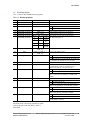
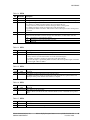
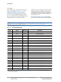
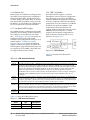
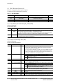
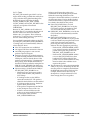
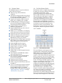
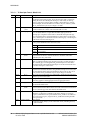
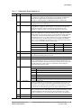
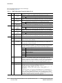
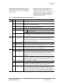
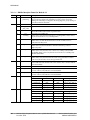
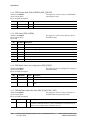
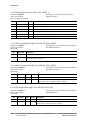
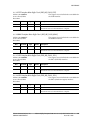
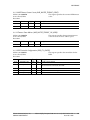
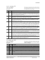
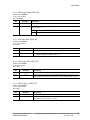
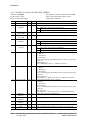
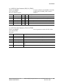
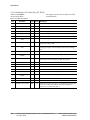
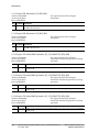
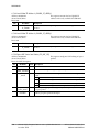
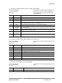
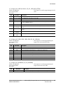
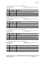
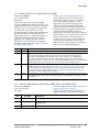
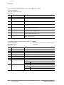
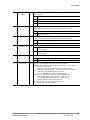
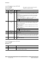
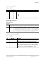
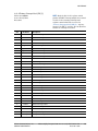
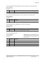
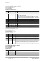
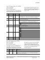
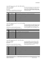
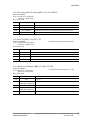
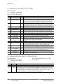
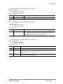
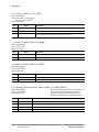
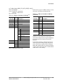
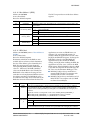
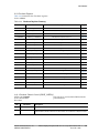
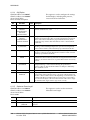
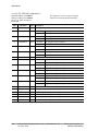
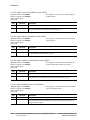
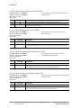
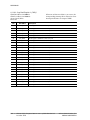
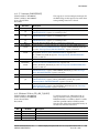
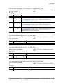
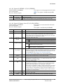
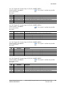
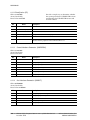
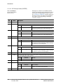
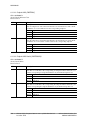
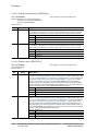
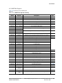
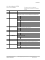
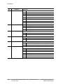
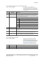
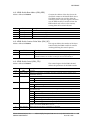
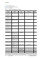
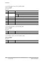
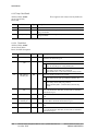
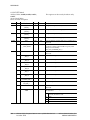
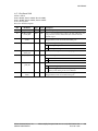
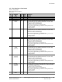
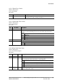
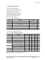
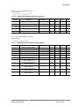
8.4.10 Ethernet XMII Control (ETH_XMII_CONTROL)
Address: 0x1805002C
Access: Read/Write
Reset: See field description
Controls the Tx and Rx clocks for the (MII/
GMII/RGMII) master mode of the GMAC. This
register should only be changed when GMAC0
is in reset.
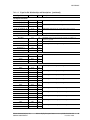
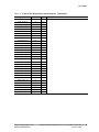
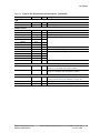
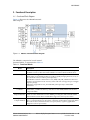
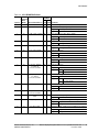
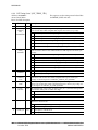
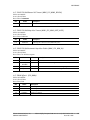
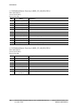
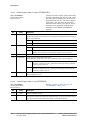
Bit
Bit Name
31
TX_INVERT
Type Reset Description
RW
0x0
Decides whether to select the inversion of the GTX clock after the delay
line
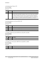
30
GIGE_QUAD
RW
0x0
Decides whether to allow a 2 ns shift (clock in the middle of a data
transfer) to the GTX clock. This bit is only effective when bit 25 is set.
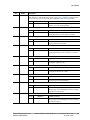
29:28
RX_DELAY
RW
0x0
The delay buffers in the Rx clock path to adjust against the edge/middlealigned RGMII inputs
27:26
TX_DELAY
RW
0x0
Delay line for the GTX clock that goes along with the data
00 Minimum delay
11 Maximum delay
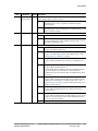
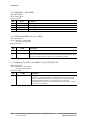
25
GIGE
RW
0x0
Set only after a 1000 Mbps connection has been negotiated
24
OFFSET
_PHASE
RW
0x0
Used to select if the start is from the positive or negative phase (or whether
to have a 180 degree change in addition to the phase-delay in [11:8].
23:16 OFFSET_CNT
RW
0x0
Beginning counter value to phase-delay the GTX clock
15:8
PHASE1_CNT
RW
0x1
Number of 100 clock cycles in the negative cycle of the XMII Tx/Rx clock
7:0
PHASE0_CNT
RW
0x1
Number of 100 clock cycles in the positive cycle of the XMII Tx/Rx clock
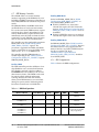
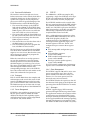
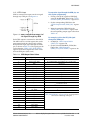
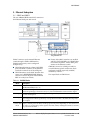
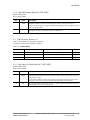
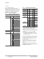
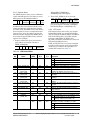
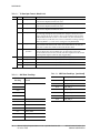
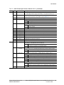
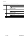
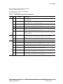
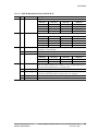
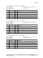
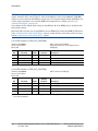
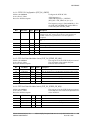
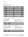
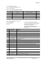
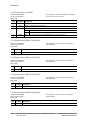
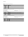
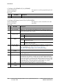
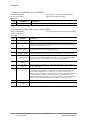
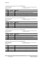
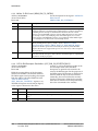
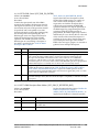
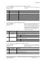
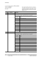
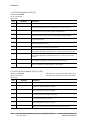
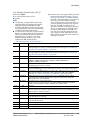
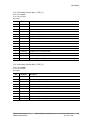
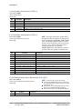
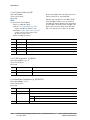
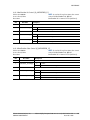
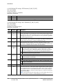
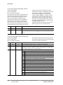
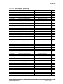
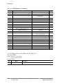
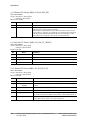
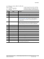
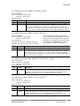
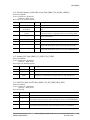
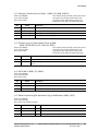
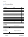
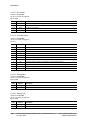
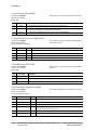
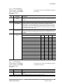
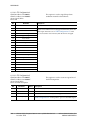
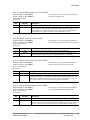
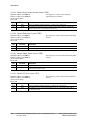
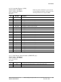
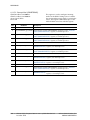
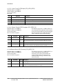
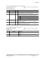
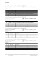
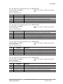
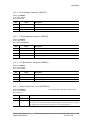
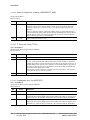
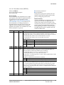
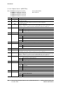
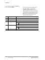
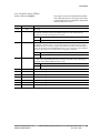
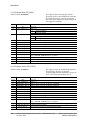
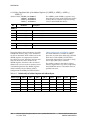
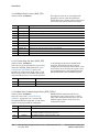
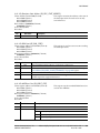
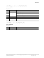
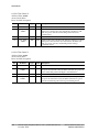
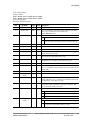
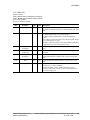
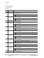
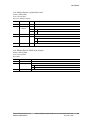
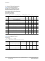
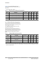
8.4.11 Audio PLL Configuration (AUDIO_PLL_CONFIG)
Address: 0x18050030
Access: Read / Write
Reset: See field description
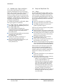
This register configures the Audio Phase Look
Loop.
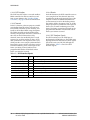
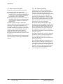
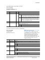
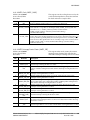
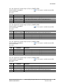
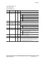
<PLL frequency> =
<REFCLK frequency>/ REFDIV *
(DIV_INT = DIV_FRAC/(218-1))/2POSTPLLDIV
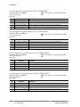
<MCLK Frequency> =
<PLL Frequency>/EXT_DIV
F_mclk = (F_REFCLK/REFDIV) *
(NINT.NFRAC)/((2POSTPLLPWD) * (EXT_DIV))
Use the “Audio PLL Modulation Control
(AUDIO_PLL_MODULATION)” on page 144
to set the DIV_INT and DIV_FRAC.
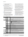
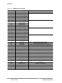
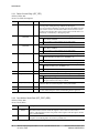
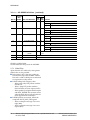
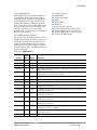
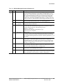
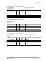
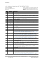
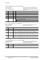
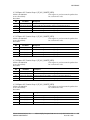
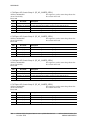
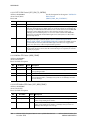
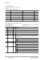
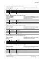
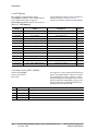
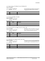
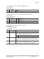
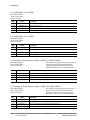
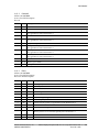
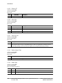
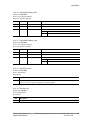
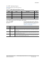
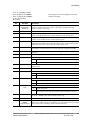
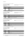
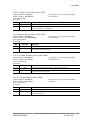
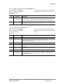
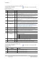
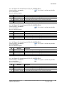
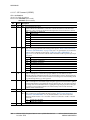
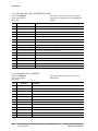
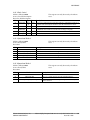
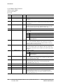
Bit
Bit Name
Type
Reset Description
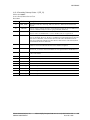
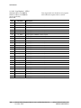
31:15
RES
RO
0x0
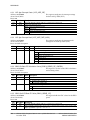
Reserved. Contains zeros when read.
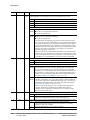
14:12
EXT_DIV
RW
0x1
Digital divider to derive the MCLK from the PLL output. Use
only even values for 50% of the duty cycle
11:10
RES
RO
0x0
Reserved. Contains zeros when read.
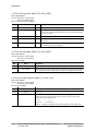
9:7
POSTPLLPWD
RW
0x1
Post power up control for the PLL
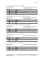
6
RES
RO
0x0
Reserved. Contains zeros when read.
5
PLLPWD
RW
0x1
Write 0 to this bit to power up the PLL
4
BYPASS
RW
0x1
Enables bypassing of the audio PLL
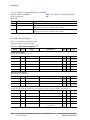
3:0
REFDIV
RW
0x1
Reference clock divider
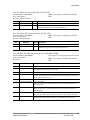
Atheros Communications, Inc.
COMPANY CONFIDENTIAL
AR9344 Highly-Integrated 802.11n 2x2 2.4/5 GHz Premium SoC
December 2010
•
•
143
143