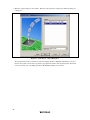
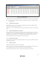
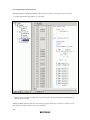
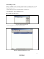
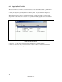
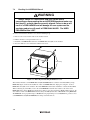
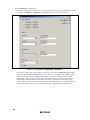
1
REJ10J1133-0600
H8/3664 E6000 Emulator
User’s Manual
Renesas Microcomputer Development Environment System
H8 Family / H8/300H Tiny Series
HS3664EPI62HE-U2
Rev.6.00
Revision Date: Feb. 05, 2007
Notes regarding these materials
1. This document is provided for reference purposes only so that Renesas customers may select the appropriate
Renesas products for their use. Renesas neither makes warranties or representations with respect to the
accuracy or completeness of the information contained in this document nor grants any license to any
intellectual property rights or any other rights of Renesas or any third party with respect to the information in
this document.
2. Renesas shall have no liability for damages or infringement of any intellectual property or other rights arising
out of the use of any information in this document, including, but not limited to, product data, diagrams, charts,
programs, algorithms, and application circuit examples.
3. You should not use the products or the technology described in this document for the purpose of military
applications such as the development of weapons of mass destruction or for the purpose of any other military
use. When exporting the products or technology described herein, you should follow the applicable export
control laws and regulations, and procedures required by such laws and regulations.
4. All information included in this document such as product data, diagrams, charts, programs, algorithms, and
application circuit examples, is current as of the date this document is issued. Such information, however, is
subject to change without any prior notice. Before purchasing or using any Renesas products listed in this
document, please confirm the latest product information with a Renesas sales office. Also, please pay regular
and careful attention to additional and different information to be disclosed by Renesas such as that disclosed
through our website. (http://www.renesas.com )
5. Renesas has used reasonable care in compiling the information included in this document, but Renesas
assumes no liability whatsoever for any damages incurred as a result of errors or omissions in the information
included in this document.
6. When using or otherwise relying on the information in this document, you should evaluate the information in
light of the total system before deciding about the applicability of such information to the intended application.
Renesas makes no representations, warranties or guaranties regarding the suitability of its products for any
particular application and specifically disclaims any liability arising out of the application and use of the
information in this document or Renesas products.
7. With the exception of products specified by Renesas as suitable for automobile applications, Renesas
products are not designed, manufactured or tested for applications or otherwise in systems the failure or
malfunction of which may cause a direct threat to human life or create a risk of human injury or which require
especially high quality and reliability such as safety systems, or equipment or systems for transportation and
traffic, healthcare, combustion control, aerospace and aeronautics, nuclear power, or undersea communication
transmission. If you are considering the use of our products for such purposes, please contact a Renesas
sales office beforehand. Renesas shall have no liability for damages arising out of the uses set forth above.
8. Notwithstanding the preceding paragraph, you should not use Renesas products for the purposes listed below:
(1) artificial life support devices or systems
(2) surgical implantations
(3) healthcare intervention (e.g., excision, administration of medication, etc.)
(4) any other purposes that pose a direct threat to human life
Renesas shall have no liability for damages arising out of the uses set forth in the above and purchasers who
elect to use Renesas products in any of the foregoing applications shall indemnify and hold harmless Renesas
Technology Corp., its affiliated companies and their officers, directors, and employees against any and all
damages arising out of such applications.
9. You should use the products described herein within the range specified by Renesas, especially with respect
to the maximum rating, operating supply voltage range, movement power voltage range, heat radiation
characteristics, installation and other product characteristics. Renesas shall have no liability for malfunctions or
damages arising out of the use of Renesas products beyond such specified ranges.
10. Although Renesas endeavors to improve the quality and reliability of its products, IC products have specific
characteristics such as the occurrence of failure at a certain rate and malfunctions under certain use
conditions. Please be sure to implement safety measures to guard against the possibility of physical injury, and
injury or damage caused by fire in the event of the failure of a Renesas product, such as safety design for
hardware and software including but not limited to redundancy, fire control and malfunction prevention,
appropriate treatment for aging degradation or any other applicable measures. Among others, since the
evaluation of microcomputer software alone is very difficult, please evaluate the safety of the final products or
system manufactured by you.
11. In case Renesas products listed in this document are detached from the products to which the Renesas
products are attached or affixed, the risk of accident such as swallowing by infants and small children is very
high. You should implement safety measures so that Renesas products may not be easily detached from your
products. Renesas shall have no liability for damages arising out of such detachment.
12. This document may not be reproduced or duplicated, in any form, in whole or in part, without prior written
approval from Renesas.
13. Please contact a Renesas sales office if you have any questions regarding the information contained in this
document, Renesas semiconductor products, or if you have any other inquiries.
IMPORTANT INFORMATION
READ FIRST
• READ this user's manual before using this emulator product.
• KEEP the user's manual handy for future reference.
Do not attempt to use the emulator product until you fully understand its mechanism.
Emulator Product:
Throughout this document, the term "emulator product" shall be defined as the following
products produced only by Renesas Technology Corp. excluding all subsidiary products.
• Emulator station
• User system interface cables
• PC interface board
• Optional SIMM memory module
• Optional board
The user system or a host computer is not included in this definition.
Purpose of the Emulator Product:
This emulator product is a software and hardware development tool for systems employing the
Renesas microcomputer (hereinafter referred to as the MCU). This emulator product must only be
used for the above purpose.
Limited Applications:
This emulator product is not authorized for use in MEDICAL, atomic energy, aeronautical or
space technology applications without consent of the appropriate officer of a Renesas sales
company. Such use includes, but is not limited to, use in life support systems. Buyers of this
emulator product must notify the relevant Renesas sales offices before planning to use the product
in such applications.
Improvement Policy:
Renesas Technology Corp. (including its subsidiaries, hereafter collectively referred to as
Renesas) pursues a policy of continuing improvement in design, performance, and safety of the
emulator product. Renesas reserves the right to change, wholly or partially, the specifications,
design, user's manual, and other documentation at any time without notice.
Target User of the Emulator Product:
This emulator product should only be used by those who have carefully read and thoroughly
understood the information and restrictions contained in the user's manual. Do not attempt to use
the emulator product until you fully understand its mechanism.
It is highly recommended that first-time users be instructed by users that are well versed in the
operation of the emulator product.
I
LIMITED WARRANTY
Renesas warrants its emulator products to be manufactured in
accordance with published specifications and free from defects in
material and/or workmanship. Renesas, at its option, will repair or
replace any emulator products returned intact to the factory,
transportation charges prepaid, which Renesas, upon inspection,
determine to be defective in material and/or workmanship.
The foregoing shall constitute the sole remedy for any breach of
Renesas' warranty. See the Renesas warranty booklet for details on
the warranty period. This warranty extends only to you, the original
Purchaser. It is not transferable to anyone who subsequently purchases
the emulator product from you. Renesas is not liable for any claim
made by a third party or made by you for a third party.
DISCLAIMER
RENESAS MAKES NO WARRANTIES, EITHER EXPRESS OR
IMPLIED, ORAL OR WRITTEN, EXCEPT AS PROVIDED
HEREIN, INCLUDING WITHOUT LIMITATION THEREOF,
WARRANTIES AS TO MARKETABILITY, MERCHANTABILITY,
FITNESS FOR ANY PARTICULAR PURPOSE OR USE, OR
AGAINST INFRINGEMENT OF ANY PATENT. IN NO EVENT
SHALL RENESAS BE LIABLE FOR ANY DIRECT, INCIDENTAL
OR CONSEQUENTIAL DAMAGES OF ANY NATURE, OR
LOSSES OR EXPENSES RESULTING FROM ANY DEFECTIVE
EMULATOR PRODUCT, THE USE OF ANY EMULATOR
PRODUCT, OR ITS DOCUMENTATION, EVEN IF ADVISED
OF THE POSSIBILITY OF SUCH DAMAGES. EXCEPT AS
EXPRESSLY STATED OTHERWISE IN THIS WARRANTY,
THIS EMULATOR PRODUCT IS SOLD "AS IS ", AND YOU
MUST ASSUME ALL RISK FOR THE USE AND RESULTS
OBTAINED FROM THE EMULATOR PRODUCT.
II
State Law:
Some states do not allow the exclusion or limitation of implied warranties or liability for
incidental or consequential damages, so the above limitation or exclusion may not apply to you.
This warranty gives you specific legal rights, and you may have other rights which may vary from
state to state.
The Warranty is Void in the Following Cases:
Renesas shall have no liability or legal responsibility for any problems caused by misuse,
abuse, misapplication, neglect, improper handling, installation, repair or modifications of the
emulator product without Renesas' prior written consent or any problems caused by the user
system.
All Rights Reserved:
This user's manual and emulator product are copyrighted and all rights are reserved by
Renesas. No part of this user's manual, all or part, may be reproduced or duplicated in any form,
in hard-copy or machine-readable form, by any means available without Renesas' prior written
consent.
Other Important Things to Keep in Mind:
1. Circuitry and other examples described herein are meant merely to indicate the characteristics
and performance of Renesas' semiconductor products. Renesas assumes no responsibility for
any intellectual property claims or other problems that may result from applications based on
the examples described herein.
2. No license is granted by implication or otherwise under any patents or other rights of any third
party or Renesas.
Figures:
Some figures in this user's manual may show items different from your actual system.
Limited Anticipation of Danger:
Renesas cannot anticipate every possible circumstance that might involve a potential hazard.
The warnings in this user's manual and on the emulator product are therefore not all inclusive.
Therefore, you must use the emulator product safely at your own risk.
III
SAFETY PAGE
READ FIRST
• READ this user's manual before using this emulator product.
• KEEP the user's manual handy for future reference.
Do not attempt to use the emulator product until you fully understand its mechanism.
DEFINITION OF SIGNAL WORDS
This is the safety alert symbol. It is used to alert you to potential personal
injury hazards. Obey all safety messages that follow this symbol to avoid
possible injury or death.
DANGER
WARNING
CAUTION
CAUTION
DANGER indicates an imminently hazardous situation which, if not
avoided, will result in death or serious injury.
WARNING indicates a potentially hazardous situation which, if not
avoided, could result in death or serious injury.
CAUTION indicates a potentially hazardous situation which, if not
avoided, may result in minor or moderate injury.
CAUTION used without the safety alert symbol indicates a
potentially hazardous situation which, if not avoided, may result
in property damage.
NOTE emphasizes essential information.
IV
WARNING
Observe the precautions listed below. Failure to do so
will result in a FIRE HAZARD and will damage the user
system and the emulator product or will result in
PERSONAL INJURY. The USER PROGRAM will be
LOST.
1. Do not repair or remodel the emulator product by
yourself for electric shock prevention and quality
assurance.
2. Always switch OFF the E6000 emulator and user system
before connecting or disconnecting any CABLES or
PARTS.
3. Always before connecting any CABLES, make sure that
pin 1 on both sides are correctly aligned.
4. Supply power according to the power specifications and
do not apply an incorrect power voltage. Use only the
provided power cable.
V
CAUTION
This equipment has been tested and found to comply
with the limits for a Class A digital device, pursuant to part 15
of the FCC Rules. These limits are designed to provide
reasonable protection against harmful interference when the
equipment is operated in a commercial environment. This
equipment generates, uses, and can radiate radio frequency
energy and, if not installed and used in accordance with the
instruction manual, may cause harmful interference to radio
communications. Operation of this equipment in a residential
area is likely to cause harmful interference in which case the
user will be required to correct the interference at his own
expense.
VI
Introduction
The E6000 emulator is an advanced realtime in-circuit emulator, which allows programs to be developed and debugged
for the H8 family microcomputers.
The E6000 emulator can either be used without a user system, for developing and debugging software, or connected via a
user system interface cable to a user system, for debugging user hardware.
High-performance Embedded Workshop is a Graphical User Interface intended to ease the development and debugging of
applications written in C/C++ programming language and assembly language for Renesas microcomputers. Its aim is to
provide a powerful yet intuitive way of accessing, observing and modifying the debugging platform in which the
application is running.
High-performance Embedded Workshop is a powerful development environment for embedded applications targeted at
Renesas microcontrollers. The main features are:
• A configurable build engine that allows you to set-up compiler, assembler and linker options via an easy to use
interface.
• An integrated text editor with user customizable syntax coloring to improve code readability.
• A configurable environment to run your own tools.
• An integrated debugger which allows you to build and debug in the same application.
• Version control support.
High-performance Embedded Workshop has been designed with two key aims; firstly to provide you, the user, with a set
of powerful development tools and, secondly, to unify and present them in a way that is easy to use.
i
About This Manual
This manual contains the following information.
Emulator Debugger Part: Preparation before use, E6000 emulator functions, debugging function, tutorial, and hardware
and software specifications of the E6000 emulator.
Refer to the High-performance Embedded Workshop User's Manual for details on the information on the basic usage of
the High-performance Embedded Workshop, customization of the environment, build functions, and debugging functions
common to each High-performance Embedded Workshop product.
This manual does not intend to explain how to write C/C++ or assembly language programs, how to use any particular
operating system or how best to tailor code for the individual devices. These issues are left to the respective manuals.
®
®
®
Microsoft , MS-DOS, Windows , Windows NT are registered trademarks of Microsoft Corporation.
Visual SourceSafe is a trademark of Microsoft Corporation.
IBM is a registered trademark of International Business Machines Corporation.
All brand or product names used in this manual are trademarks or registered trademarks of their respective companies or
organizations.
Document Conventions
This manual uses the following typographic conventions:
Table 1
Typographic Conventions
Convention
Meaning
[Menu->Menu Option]
Bold text with ‘->’ is used to indicate menu options
(for example, [File->Save As...]).
FILENAME.C
Uppercase names are used to indicate filenames.
“enter this string”
Used to indicate text that must be entered (excluding the “” quotes).
Key + Key
Used to indicate required key presses. For example, CTRL+N means
press the CTRL key and then, whilst holding the CTRL key down,
press the N key.
(The “how to” symbol)
When this symbol is used, it is always located in the left hand margin.
It indicates that the text to its immediate right is describing “how to”
do something.
Components
Check all the components described in the component list unpacking. If the components are not complete, contact a
Renesas sales office.
ii
Contents
Emulator Debugger Part
Section 1 Overview........................................................................................... 1
1.1
1.2
1.3
1.4
Features .............................................................................................................................1
Warnings ...........................................................................................................................2
Environmental Conditions ................................................................................................3
Emulator External Dimensions and Mass .........................................................................3
Section 2 Preparation before Use...................................................................... 5
2.1
2.2
2.3
Emulator Preparation ........................................................................................................5
Installing Emulator’s Software .........................................................................................5
Connecting to the User System .........................................................................................6
2.3.1 Example of Connecting the User System Interface Cable Head
to the User System...............................................................................................6
2.3.2 Plugging the User System Interface Cable Body into the Emulator ....................7
2.3.3 Plugging the User System Interface Cable Body into the Cable Head ................7
2.4 Power Supply ....................................................................................................................8
2.4.1 AC Adapter ..........................................................................................................8
2.4.2 Polarity.................................................................................................................8
2.4.3 Power Supply Monitor Circuit .............................................................................8
2.5 SIMM Memory Module....................................................................................................8
2.5.1 Optional SIMM Memory Module Configuration.................................................8
2.6 Hardware Interface............................................................................................................9
2.6.1 Signal Protection on the emulator ........................................................................9
2.6.2 User System Interface Circuits.............................................................................9
2.6.3 Clock Oscillator ...................................................................................................9
2.6.4 External Probe 1 (EXT1)/Trigger Output ............................................................9
2.6.5 External Probe 2 (EXT2)/Trigger Output ............................................................10
2.6.6 Voltage Follower Circuit .....................................................................................11
2.7 System Check ......................................................................................................................12
2.8 Communication Problems .................................................................................................17
2.9 Other Methods for Activating the Emulator ........................................................................17
2.10 Uninstalling the Emulator’s Software................................................................................17
Section 3 E6000 Emulator Functions ............................................................... 19
3.1
3.2
3.3
Debugging Features ..........................................................................................................19
3.1.1 Breakpoints ..........................................................................................................19
3.1.2 Trace ....................................................................................................................19
3.1.3 Execution Time Measurements............................................................................19
3.1.4 Performance Analysis ..........................................................................................19
3.1.5 Bus Monitoring ....................................................................................................20
Complex Event System (CES) ..........................................................................................20
3.2.1 Event Channels ....................................................................................................20
3.2.2 Range Channels ...................................................................................................21
3.2.3 Breaks ..................................................................................................................21
3.2.4 Timing..................................................................................................................21
Hardware Features ............................................................................................................22
3.3.1 Memory................................................................................................................22
3.3.2 Clocks ..................................................................................................................23
iii
3.3.3 Probes .................................................................................................................. 23
3.4 Stack Trace Function ........................................................................................................... 23
3.5 Online Help.......................................................................................................................... 23
Section 4 Preparation before Use ......................................................................25
4.1
Method for Activating High-performance Embedded Workshop..................................... 25
4.1.1 Creating a New Workspace (Toolchain Not Used).............................................. 26
4.1.2 Creating a New Workspace (Toolchain Used)....................................................... 30
4.1.3 Selecting an Existing Workspace........................................................................... 34
4.2 Connecting the Emulator ..................................................................................................... 35
4.3 Reconnecting the Emulator.................................................................................................. 36
4.4 Ending the Emulator ............................................................................................................ 36
Section 5 Debugging .........................................................................................37
5.1
5.2
5.3
5.4
5.5
5.6
5.7
iv
Setting the Environment for Emulation ............................................................................ 38
5.1.1 Opening the [Configuration Properties] Dialog Box ........................................... 38
5.1.2 Selecting an MCU Not Included in the List......................................................... 40
5.1.3 Selecting the Interface to be Connected............................................................... 41
5.1.4 Opening the [Memory Mapping] Dialog Box...................................................... 42
5.1.5 Changing the Memory Map Setting..................................................................... 43
Downloading a Program ................................................................................................... 44
5.2.1 Downloading a Program ...................................................................................... 44
5.2.2 Viewing the Source Code .................................................................................... 45
5.2.3 Viewing the Assembly-Language Code............................................................... 48
5.2.4 Modifying the Assembly-Language Code ........................................................... 49
5.2.5 Viewing a Specific Address................................................................................. 49
5.2.6 Viewing the Current Program Counter Address .................................................. 49
Viewing the Current Status ............................................................................................... 50
Reading and Displaying the Emulator Information Regularly.......................................... 51
5.4.1 Opening the [Extended Monitor] Window .......................................................... 51
5.4.2 Selecting Items to be Displayed........................................................................... 52
Displaying Memory Contents in Realtime........................................................................ 53
5.5.1 Opening the [Monitor] Window .......................................................................... 53
5.5.2 Changing the Monitor Settings ............................................................................ 55
5.5.3 Temporarily Stopping Update of the Monitor ..................................................... 55
5.5.4 Deleting the Monitor Settings .............................................................................. 55
5.5.5 Monitoring Variables ........................................................................................... 55
5.5.6 Hiding the [Monitor] Window ............................................................................. 56
5.5.7 Managing the [Monitor] Window ........................................................................ 57
Viewing the Variables....................................................................................................... 58
5.6.1 [Watch] Window.................................................................................................. 58
Using the Event Points ...................................................................................................... 60
5.7.1 Software Breakpoints........................................................................................... 60
5.7.2 Event Points ......................................................................................................... 60
5.7.3 Event Detection System....................................................................................... 60
5.7.4 Signals to Indicate Bus States and Areas ............................................................. 61
5.7.5 Opening the [Event] Window .............................................................................. 62
5.7.6 Setting Software Breakpoints............................................................................... 62
5.7.7 Setting Event Points............................................................................................. 64
5.7.8 Setting Trigger Points .......................................................................................... 72
5.7.9 Editing Event Points ............................................................................................ 73
5.7.10 Modifying Event Points ....................................................................................... 73
5.7.11 Enabling an Event Point....................................................................................... 73
5.8
5.9
5.7.12 Disabling an Event Point......................................................................................73
5.7.13 Deleting an Event Point .......................................................................................73
5.7.14 Deleting All Event Points ....................................................................................73
5.7.15 Viewing the Source Line for an Event Point........................................................73
Viewing the Trace Information .........................................................................................74
5.8.1 Opening the [Trace] Window ..............................................................................74
5.8.2 Acquiring Trace Information ...............................................................................74
5.8.3 Specifying Trace Acquisition Conditions ............................................................76
5.8.4 Searching for a Trace Record...............................................................................84
5.8.5 Clearing the Trace Information............................................................................93
5.8.6 Saving the Trace Information in a File.................................................................93
5.8.7 Viewing the [Editor] Window..............................................................................94
5.8.8 Trimming the Source ...........................................................................................94
5.8.9 Acquiring a Snapshot of the Trace Information...................................................94
5.8.10 Temporarily Stopping Trace Acquisition.............................................................94
5.8.11 Restarting Trace Acquisition ...............................................................................94
5.8.12 Extracting Records from the Acquired Information.............................................95
5.8.13 Calculating the Difference in Time Stamping......................................................105
5.8.14 Analyzing Statistical Information ........................................................................106
5.8.15 Extracting Function Calls from the Acquired Trace Information ........................107
Analyzing Performance.....................................................................................................108
5.9.1 Opening the [Performance Analysis] Window ....................................................110
5.9.2 Setting Conditions for Measurement ...................................................................111
5.9.3 Selecting the Address Detection Mode and Resolution .......................................118
5.9.4 Starting Performance Data Acquisition ...............................................................118
5.9.5 Deleting a Measurement Condition .....................................................................118
5.9.6 Deleting All Measurement Conditions.................................................................118
Section 6 Tutorial.............................................................................................. 119
6.1 Introduction..........................................................................................................................119
6.2 Running the High-performance Embedded Workshop ........................................................120
6.3 Downloading the Tutorial Program .....................................................................................121
6.3.1 Downloading the Tutorial Program........................................................................121
6.3.2 Displaying the Source Program..............................................................................122
6.4 Setting a Software Breakpoint .............................................................................................123
6.5 Setting Registers ..................................................................................................................124
6.6 Executing the Program.........................................................................................................125
6.7 Reviewing Breakpoints ........................................................................................................128
6.8 Referring to Symbols ...........................................................................................................129
6.9 Viewing Memory.................................................................................................................130
6.10 Watching Variables............................................................................................................131
6.11 Displaying Local Variables................................................................................................134
6.12 Stepping Through a Program .............................................................................................135
6.12.1 Executing the [Step In] Command .......................................................................135
6.12.2 Executing the [Step Out] Command ....................................................................137
6.12.3 Executing the [Step Over] Command ..................................................................138
6.13 Forced Breaking of Program Executions ...........................................................................139
6.14 Resetting the MCU ............................................................................................................139
6.15 Break Function...................................................................................................................140
6.15.1 Software Break Function......................................................................................140
6.15.2 Breaking Execution at Event Points .....................................................................145
6.16 Trace Functions..................................................................................................................149
6.16.1 Displaying a Trace (when Time Stamping is not Available) ...............................150
v
6.17
6.18
6.19
6.20
6.16.2 Displaying a Trace (when Time Stamping is Available) ..................................... 156
6.16.3 Statistics ............................................................................................................... 160
6.16.4 Function Calls ...................................................................................................... 164
Stack Trace Function ......................................................................................................... 165
Performance Measurement Function ................................................................................. 167
6.18.1 Time Of Specified Range Measurement .............................................................. 167
Monitor Function ............................................................................................................... 170
What Next? ........................................................................................................................ 172
Section 7 Hardware Specifications Specific to This Product ............................173
7.1
7.2
7.3
7.4
7.5
H8/3664 E6000 Emulator Specifications.......................................................................... 173
7.1.1 Supported Items ................................................................................................... 173
7.1.2 Operating Voltage and Frequency Specifications ................................................ 174
User System Interface.......................................................................................................... 175
7.2.1 Signal Protection.................................................................................................. 175
7.2.2 User System Interface Circuits ............................................................................ 175
Differences between MCU and Emulator ......................................................................... 177
7.3.1 A/D Converter and D/A Converter ...................................................................... 177
Handling Serial EEPROM Board...................................................................................... 178
Host PC Interface.............................................................................................................. 179
Section 8 Software Specifications Specific to This Product .............................181
8.1
8.2
Software Specifications of the H8/3664 E6000 Emulator ................................................ 181
8.1.1 Target Hardware .................................................................................................. 181
8.1.2 Selectable Platforms............................................................................................. 181
8.1.3 [Configuration Properties] Dialog Box ([General] Page) .................................... 182
8.1.4 [Configuration Properties] Dialog Box ([Custom] Page)..................................... 187
8.1.5 Memory Mapping Function ................................................................................. 190
8.1.6 [Status] Window .................................................................................................. 190
8.1.7 Extended Monitor Function ................................................................................. 192
8.1.8 Signals to Indicate Bus States and Areas ............................................................. 193
8.1.9 Monitoring Function ............................................................................................ 193
8.1.10 Trigger Points ...................................................................................................... 193
8.1.11 Trace Information ................................................................................................ 194
8.1.12 Searching for a Trace Record............................................................................... 195
8.1.13 Trace Filtering Function ...................................................................................... 195
8.1.14 Reading from and Writing to the EEPROM ........................................................ 196
Notes on Usage of the H8/3664 E6000 Emulator ............................................................. 202
8.2.1 I/O Register.......................................................................................................... 202
8.2.2 Notes on Mode Transitions .................................................................................. 226
8.2.3 Access to the Reserved Area................................................................................ 226
8.2.4 Environment for Execution of the Tutorial Program ........................................... 226
8.2.5 Note on Emulation of the H8/36912 Group and H8/36902 Group ...................... 227
Appendix A I/O File Format .............................................................................229
A.1
A.2
File format (Bit Field Not Supported)............................................................................... 229
File format (Bit Field Supported)...................................................................................... 231
Appendix B Menus............................................................................................233
Appendix C Command Lines ............................................................................237
Appendix D Diagnostic Test Procedure ............................................................241
vi
D.1
D.2
System Set-Up for Test Program Execution .....................................................................241
Diagnostic Test Procedure Using Test Program ...............................................................242
vii
viii
Emulator Debugger Part
Section 1 Overview
1.1
Features
• The breakpoint, memory map, performance, and trace can be set through the dialog box.
⎯ Intuitive user interface
⎯ Online help
⎯ Common display and operability
• Supported host interfaces
The PCI interface, PC card (PCMCIA) interface, USB interface, or LAN interface can be used for connecting
to the host computer.
• Realtime emulation
Realtime emulation of the user system is enabled at the maximum operating frequency of the CPU.
• Excellent operability
Using the High-performance Embedded Workshop enables user program debugging using a pointing device
such as a mouse. The High-performance Embedded Workshop enables high-speed downloading of load
module files.
• Various debugging functions
Various break and trace functions enable efficient debugging. Breakpoints and break conditions can be set
by the specific window, trace information can be displayed on a window, and command-line functions can be
used.
• Memory access during emulation
During emulation, the memory contents can be read and modified.
1
1.2
Warnings
CAUTION
READ the following warnings before using the emulator product.
Incorrect operation will damage the user system and the emulator
product. The USER PROGRAM will be LOST.
1. Check all components against the component list after unpacking the emulator.
2. Never place heavy objects on the casing.
3. Do not place the emulator in places where:
•
The temperature becomes high such as in direct sunlight or near a heater. For details, refer to section 1.3,
Environmental Conditions.
•
The temperature or humidity changes greatly.
•
There is a lot of dust.
•
There is a lot of vibration. For details, refer to section 1.3, Environmental Conditions.
4. Protect the emulator from excessive impacts and stresses.
5. Only supply the specified voltage and power-supply frequency.
6. When moving the emulator, take care not to vibrate or damage it.
7. After connecting the cable, check that it is connected correctly. For details, refer to section 2, Preparation
before Use. Supply power to the connected equipment after connecting all cables. For the supplying
procedures, refer to section 2.7, System Check. Cables must not be connected or disconnected while the
power is on.
2
1.3
Environmental Conditions
CAUTION
Observe the conditions listed in table 1.1 when using the emulator.
Failure to do so will cause illegal operation in the user system, the
emulator product, and the user program.
Table 1.1 Environmental Conditions
Item
Specifications
Temperature
Operating: +10°C to +35°C
Storage: –10°C to +50°C
Humidity
Operating: 35% RH to 80% RH, no condensation
Storage: 35% RH to 80% RH, no condensation
Vibration
Operating:
2.45 m/s max.
2
Storage:
4.9 m/s max.
2
Transportation: 14.7 m/s max.
Ambient gases
No corrosive gases may be present
1.4
2
Emulator External Dimensions and Mass
Table 1.2 Emulator External Dimensions and Mass
Item
Specifications
Dimensions
219 × 170 × 54 mm
Mass
Approximately 850 g
3
4
Section 2 Preparation before Use
2.1
Emulator Preparation
Unpack the emulator and prepare it for use as follows:
WARNING
READ the reference sections shaded in figure 2.1 before using the
emulator product. Incorrect operation will damage the user system and
the emulator product. The USER PROGRAM will be LOST.
Reference
Unpack the emulator
Component list
Check the components against
the component list
Setup
Set up the emulator
- Insert the optional board
- Install the High-performance Embedded Workshop
- Connect the interface cable
Turn on the user system
(Only when the user system is connected)
Section 3
Section 4
Turn on the emulator
Activation
Start the High-performance Embedded Workshop
Figure 2.1 Emulator Preparation Flowchart
2.2
Installing Emulator’s Software
To install the High-performance Embedded Workshop, refer to the Setup Guide for the E6000 Emulator supplied
together with the emulator.
5
2.3
Connecting to the User System
To connect the emulator to a user system, proceed as follows:
• Connect the user system interface cable head to the user system.
• Plug the cable body into the emulator.
• Plug the cable body into the cable head.
For details of these steps, refer to the User System Interface Cable User’s Manual.
Figure 2.2 gives details of the connectors provided on the emulator.
PC interface cable
connector
USB interface cable
connector
User system
interface connector
Power connector
POWER RUN
Power switch
External probe
connector
Screw
Screw
Figure 2.2 E6000 Emulator Connectors
2.3.1
Example of Connecting the User System Interface Cable Head to the User System
Screw (× 4)
User system interface
cable head
IC socket
Figure 2.3 Example of Connecting User System Interface Cable Head to User System
• Ensure that all power is off to the emulator and the user system.
• Insert the cable head into the socket on the user system.
Note: Depending upon the package, it may be possible to orientate this cable head in any position on the socket,
so care should be taken to correctly identify pin 1 on the emulator and socket when installing.
6
• Screw the cable head to the socket with the screws provided. Progressively tighten the screws in the sequence
shown in figure 2.4 until all are ‘finger tight’.
1
3
4
2
Figure 2.4 Sequence of Screw Tightening
Note: Be careful not to over-tighten the screws as this may result in contact failure on the user system or
damage the cable head. Where provided, use the ‘solder lugs’ on the QFP socket to provide extra
strength to the emulator/user system connection.
2.3.2
Plugging the User System Interface Cable Body into the Emulator
Plug the cable body into the emulator, taking care to insert it straight, and push it firmly into place.
User system interface cable body
User system interface cable head
EXT2
POWER RUN
EXT1
Emulator
User system interface cable
Figure 2.5 Plugging User System Interface Cable Body to Emulator
2.3.3
Plugging the User System Interface Cable Body into the Cable Head
Plug the cable body into the cable head on the user system.
7
2.4
Power Supply
2.4.1
AC Adapter
The AC adapter supplied with the emulator must be used at all times.
2.4.2
Polarity
Figure 2.6 shows the polarity of the power-supply plug.
5 V (outside)
GND (inside)
Figure 2.6 Polarity of Power Supply Plug
2.4.3
Power Supply Monitor Circuit
The emulator incorporates a power supply monitor circuit which only lights the green LED when a voltage
higher than 4.75 V is supplied. If this LED is not illuminated, you should check the emulator voltage level. An
input voltage less than 4.75 V could indicate that enough current cannot be supplied to the emulator.
Note: Use the provided AC adapter for the emulator.
2.5
SIMM Memory Module
E6000 emulator’s optional SIMM memory modules are available which provide emulation memory for user
code without needing a user system. The optional SIMM memory modules are available in different memory
size, but all are partitioned into four equal banks. These banks can be relocated on page boundaries anywhere in
the user area. Note that, however, some products do not support the SIMM memory module.
2.5.1
Optional SIMM Memory Module Configuration
The configuration of the optional SIMM memory module is controlled by the mapping RAM. Opening the
[Memory] sheet of the [System Status] window allows you to check which optional SIMM memory module, if
any, is installed and also allows the four banks to be relocated to the required addresses from the [Memory
Mapping] dialog box.
8
2.6
Hardware Interface
All signals are directly connected to the MCU in the emulator with no buffering with the exception of those
listed in section 7, Hardware Specifications Specific to This Product.
2.6.1
Signal Protection on the emulator
All signals are over/under voltage protected by use of diode arrays. The only exceptions being the AVCC and Vref.
All ports have pull-up resistors except for analog port.
All VCC pins on the cable head assembly are connected together (with the exception of the AVCC pin), and are
then monitored by the emulator to detect powered user system presence.
2.6.2
User System Interface Circuits
The interface circuit between the MCU in the emulator and the user system has a signal delay of about 8 ns due
to the user system interface cable and it includes pull-up resistors. Therefore, high-impedance signals will be
pulled up to the high level. When connecting the emulator to a user system, adjust the user system to compensate
for propagation delays.
The following diagrams show the equivalent circuit examples of the interface signals. The interface circuits
depend on the MCU type. For details, refer to section 7, Hardware Specifications Specific to This Product.
2.6.3
Clock Oscillator
The oscillator circuit has been implemented on the user system interface cable head. For details on the oscillator
circuit, refer to the user's manual for each user system interface cable.
2.6.4
External Probe 1 (EXT1)/Trigger Output
An 8-pin connector, marked EXT1 (on the right under the user system interface cable connector), on the
emulator case accommodates four external probe inputs and two trigger outputs. The pin assignment of this
connector is shown in figure 2.7.
EXT1
1
2
3
Probe
4
GND GND
TUVCC T5V
Trigger output
Figure 2.7 External Probe Connector 1
9
The interface circuit for the external probe 1 is shown in figure 2.8.
Vcc
10 kΩ
External probe 1, 2, 3, 4
HD151015
22 Ω
Figure 2.8 Interface Circuit for External Probe 1
The trigger output is controlled by event channel 8 and is an active low signal. The trigger output is available as
either T5V (within the range from 2.5 V to 5 V; does not depend on the user VCC level) or TUVCC (the user VCC
level).
2.6.5
External Probe 2 (EXT2)/Trigger Output
A 6-pin connector, marked EXT2 (on the left under the user system interface cable connector), on the emulator
case accommodates four trigger outputs. The pin assignment of this connector is shown in figure 2.9.
EXT2
5
1
2
3
6
4
Trigger output
Figure 2.9 External Probe 2 Connector
The trigger output is an active high signal which is output during the read or write cycles when a trace condition
(1 to 4) of the bus monitor function is satisfied. The trigger output is available as user VCC level. Note that,
however, some products do not support the external probe 2 (EXT2).
10
2.6.6
Voltage Follower Circuit
CAUTION
1. Do not connect the user system interface cable to the emulator
without user system connection.
2. Turn on the user system before starting up the emulator.
A voltage follower circuit is implemented on the emulator which allows the user system voltage level from the
user system to be monitored. This monitored voltage level is automatically supplied to the logic on the emulator
and is derived from the emulator power supply unit. This means that no power is taken from the user system
board.
If no user system interface cable is connected to the emulator, the emulator will operate at a specified voltage
and all clock frequencies will be available to the user. If the user system interface cable is attached, the emulator
will match the voltage supplied to the user target in all cases; i.e. even when the user VCC is below the operating
voltage for the MCU. You must be careful not to select an invalid clock frequency. When the emulator is
connected to the user system and the user system is turned off, the voltage follower circuit output voltage level is
0 V. In this case, the emulator will not operate correctly.
You can set a user VCC threshold in the range Vcc max. – 0 V by using the emulator configuration dialog box. If
the user VCC drops below this threshold, [User System Voltage] in the [Extended Monitor] window will display
Down, otherwise OK is displayed.
3.3 V
User
threshold
User Vcc level
0V
User Vcc
threshold
OK
Down
3.3 V
E6000
Vcc level
0V
The user system interface
cable is not connected.
Figure 2.10 Voltage Level Monitoring (Example for Vcc = 3.3 V)
11
2.7 System Check
When the software is executed, use the procedure below to check that the emulator is connected correctly. Here,
use the workspace for a tutorial provided on the product.
Refer to section 2.9, Other Methods for Activating the Emulator, for the other activating method to create a new
project or use a workspace for the High-performance Embedded Workshop of the old version.
1. Connect the emulator to the host computer.
2. Connect the user system interface cable to the connector of the emulator.
3. Turn on the emulator.
4. Activate the High-performance Embedded Workshop from the [Programs] in the [Start] menu (figure 2.11).
Figure 2.11 [Start] Menu
Note: If ‘LAN Driver’ is not selected at installation, [Tools] is not displayed.
12
5. The [Welcome!] dialog box is displayed.
Figure 2.12 [Welcome!] Dialog Box
To use a workspace for the tutorial, select the [Browse to another project workspace] radio button and click the
[OK] button.
When the [Open Workspace] dialog box is opened, specify the following directory:
OS installation drive \Workspace\Tutorial\E6000\xxxx
Note: The directory mentioned above cannot be specified depending on the version of the software. In such
cases, specify the following directory instead.
High-performance Embedded Workshop installation destination directory
\Tools\Renesas\DebugComp\Platform\E6000\xxxx\Tutorial
After the directory has been specified, select the following file and click the [Open] button.
Figure 2.13 [Open Workspace] Dialog Box
13
When no compiler package or that of a different version is installed, the following message box will be displayed.
Figure 2.14 Message Box
6. The [E6000 Driver Details] dialog box is displayed. This dialog box is only displayed at the first initiation.
When only one of interface drivers is selected, this dialog box is not displayed.
Figure 2.15 [E6000 Driver Details] Dialog Box
• In the [Driver] combo box, select the driver to connect the emulator.
• [Interface] displays the name of the interface to be connected.
• Click the [Close] button.
14
7. Set up the emulator. During this process, the following dialog box is displayed.
Figure 2.16 [Connecting] Dialog Box
15
8. When "Connected" is displayed in the [Output] window of the High-performance Embedded Workshop, the
emulator initiation is completed.
Figure 2.17 High-performance Embedded Workshop Window
16
2.8
Communication Problems
The following message box will be displayed when the emulator power is turned off or the PC interface cable is
not correctly connected.
Figure 2.18 Error Message
For information on other errors, refer to the Setup Guide for the E6000 Emulator.
2.9 Other Methods for Activating the Emulator
Refer to section 4, Preparation before Use.
2.10 Uninstalling the Emulator’s Software
For details on uninstallation, refer to the Setup Guide for the E6000 Emulator.
17
18
Section 3 E6000 Emulator Functions
3.1
Debugging Features
3.1.1
Breakpoints
The emulator provides a comprehensive range of alternative types of breakpoints, to give you the maximum
flexibility in debugging applications and user system.
Hardware Break Conditions: Up to 12 break conditions can be defined using the event and range channels in
the complex event system (CES). For more information about the hardware break conditions, see section 3.2,
Complex Event System (CES).
Software Breakpoints: Up to 256 software breakpoints can be defined. These software breakpoints are set by
replacing the user instruction by a BREAK instruction. In target ROM, only one breakpoint (on-chip break) can
be set.
3.1.2
Trace
The emulator incorporates a powerful realtime trace facility which allows you to examine MCU activity in detail.
The realtime trace buffer holds up to 32768 bus cycles, and it is continuously updated during execution. The
buffer is configured as a rolling buffer, which can be stopped during execution and read back by the host
computer without halting emulation.
The data stored in the trace buffer is displayed in both source program and assembly languages for ease of
debugging. However, if trace filtering is used, only assembly language can be displayed.
The buffer can be set up to store all bus cycles or just selected cycles. This is called trace acquisition and uses the
complex event system (CES) to select the parts of the program you are interested in.
It is also possible to store all bus cycles and then just look at selected cycles. This is called trace filtering.
3.1.3
Execution Time Measurements
The emulator allows you to measure the total execution time, or to measure the time of execution between
specified events in the complex event system. You can set the resolution of the timer to any of the following
values:
20 ns, 125 ns, 250 ns, 500 ns, 1 µs, 2 µs, 4 µs, 8 µs, or 16 µs.
At 20 ns the maximum time that can be measured is about six hours, and at 16µs the maximum time is about 200
days.
3.1.4
Performance Analysis
The emulator provides functions for measuring the performance of a program. The performance of the specified
program range can be displayed either as a histogram or in percentage form. A timer resolution of 20 ns, 40 ns,
or 160 ns can be selected. In addition, the execution count of the specified program range can be measured (1 to
65535).
19
3.1.5
Bus Monitoring
The emulator incorporates a bus monitoring function that monitors and displays the contents of the accessed area
in High-performance Embedded Workshop windows without stopping the program execution. Up to eight
blocks of 256 bytes can be monitored. In addition, the emulator can output trigger signals from external probe 2
(EXT2) when specified addresses (four points max.) are accessed. Note that, however, some products do not
support the bus monitoring function.
3.2
Complex Event System (CES)
In most practical debugging applications, the program or hardware errors that you are trying to debug occur
under a certain restricted set of circumstances. For example, a hardware error may only occur after a specific
area of memory has been accessed. Tracking down such problems using simple software breakpoints can be very
time-consuming.
The emulator provides a very sophisticated system for giving a precise description of the conditions you want to
examine, called the complex event system. This allows you to define events which depend on the state of a
specified combination of the MCU signals.
The complex event system provides a unified way of controlling the trace, break, and timing functions of the
emulator.
3.2.1
Event Channels
The event channels allow you to detect when a specified event has occurred. The event can be defined as a
combination of one or more of the followings:
• Address or address range
• Address outside range
• Read or Write or either
• Data, with an optional mask
• MCU access type (e.g., DMAC and instruction prefetch)
• MCU access area (e.g., on-chip ROM and on-chip RAM)
• A signal state on one or more of the four external probes
• A certain number of times that the event must be triggered
• Delay cycles after an event
Up to eight events can be combined into a sequence, in which each event is either activated or deactivated by the
occurrence of the previous event in the sequence. For example, you can cause a break if an I/O register is written
to after a specified area of RAM has been accessed.
20
3.2.2
Range Channels
The range channels can be set up to be triggered on a combination of one or more of the following:
• Address or address range (inside the range)
• Read or Write or either
• Data, with an optional mask
• MCU access type (e.g., DMAC and instruction prefetch)
• MCU access area (e.g., on-chip ROM and on-chip RAM)
• A signal state on one or more of the four external probes
• Delay cycles after an event
The complex event system can be used to control the following functions of the emulator:
3.2.3
Breaks
Use breaks to interrupt program execution when a specified event, or sequence of events, is activated. For
example, you can set up a break to halt execution when the program reads from one address, and then writes to
another address. The break can also optionally be delayed by up to 65535 bus cycles.
3.2.4
Timing
You can set up two events and then measure the execution time of the program between the activation of the first
event and second event.
21
3.3
Hardware Features
3.3.1
Memory
The emulator provides standard emulation memory as the substitute for on-chip ROM memory and on-chip
RAM memory. When a device type or device mode without an on-chip ROM or on-chip RAM is selected, the
standard emulation memory is disabled. When debugging with only the emulator and the user program and data
are stored in an external address space, an optional SIMM memory module must be used. The optional SIMM
memory modules can be separately purchased.
The emulation memory can be mapped in 64-byte units to any number of separate memory blocks in the MCU
address space. Each memory block can be specified using the memory mapping function as user (Target) or
emulator (SIMM memory module) and, in each case, the access can be specified as read-write, read-only, or
guarded.
The definition of each type of memory is as follows:
Table 3.1
Memory Types
Memory Type
Description
On-chip
Uses the MCU on-chip memory.
User
Accesses the user system memory.
Emulator
Accesses the emulator SIMM memory module.
The contents of a specified block of memory can be displayed using the memory function. The contents of
memory can be modified at any time, even during program execution and the results are immediately reflected in
all other appropriate windows.
Note that modifying memory contents during program execution has the following time requirements:
1. MCU on-chip ROM or RAM, or emulator SIMM memory module
The emulator modifies the memory contents by temporarily switching the memory bus to the emulator side
without stopping the user program execution. Therefore, the emulator uses the memory bus for up to 80 µs in
reading of 256 bytes (25 MHz, on-chip ROM).
2. MCU on-chip I/O, DTCRAM, or user system memory
The emulator stops the user program execution, then modifies the memory contents. Therefore, the user
program stops for a maximum of 2 ms in reading 256 bytes (25 MHz, emulation memory).
22
3.3.2
Clocks
The clock can be specified as emulator internal clock or target clock. The frequencies that can be specified as
the emulator internal clock depend on the MCU. For details, refer to section 8, Software Specifications Specific
to This Product.
3.3.3
Probes
External probes 1 and 2 (EXT1 and EXT2) can be connected to the emulator, to make use of signals on the user
system for break or trace. The signal for external probe 1 can be set as the condition for the event detection
system depending on the low or high level. Since the signal for external probe 2 outputs high level when the
trigger setting (1 to 4) condition is matched in the bus monitor function, the signal can be used for the trigger
condition for such as an oscilloscope.
3.4 Stack Trace Function
The emulator uses the stack’s information to display the name of the calling function for a function at which the
program counter is currently pointing. This function can be used only when the load module that has the
Dwarf2-type debugging information is loaded. For the usage of this function, refer to section 6.17, Stack Trace
Function.
3.5 Online Help
An online help explains the usage of each function or the command syntax that can be entered from the
command line window.
Select [Emulator Help] from the [Help] menu to view the emulator help.
23
24
Section 4 Preparation before Use
4.1
Method for Activating High-performance Embedded Workshop
To activate the High-performance Embedded Workshop, follow the procedure listed below.
1. Connect the emulator to the host computer.
2. Connect the user system interface cable to the connector of the emulator if you use the user system interface
cable. This is not necessary when you do not use the user system interface cable.
3. Turn on the emulator. Be sure to turn on the user system before supplying power to the emulator if you use
the user system.
4. Activate the High-performance Embedded Workshop from [Programs] in the [Start] menu.
5.
The [Welcome!] dialog box is displayed.
Figure 4.1 [Welcome!] Dialog Box
[Create a new project workspace] radio button: Creates a new workspace.
[Open a recent project workspace] radio button: Uses an existing workspace and displays the history of the
opened workspace.
[Browse to another project workspace] radio button: Uses an existing workspace; this radio button is used when
the history of the opened workspace does not remain.
In this section, we describe the following three ways to start up the High-performance Embedded Workshop:
•
[Create a new project workspace] - a toolchain is not in use
•
[Create a new project workspace] - a toolchain is in use
•
[Browse to another project workspace]
The method to create a new workspace depends on whether a toolchain is or is not in use. Note that this emulator
product does not include a toolchain. Use of a toolchain is available in an environment where the H8S, H8/300
series C/C++ compiler package has been installed. For details on this, refer to the manual attached to the H8S,
H8/300 series C/C++ compiler package.
25
4.1.1
Creating a New Workspace (Toolchain Not Used)
1. In the [Welcome!] dialog box that is displayed when the High-performance Embedded Workshop is activated,
select [Create a new project workspace] radio button and click the [OK] button.
Figure 4.2 [Welcome!] Dialog Box
26
2. Creation of a new workspace is started. The following dialog box is displayed.
Figure 4.3 [New Project Workspace] Dialog Box
[Workspace Name] edit box: Enter the new workspace name.
[Project Name] edit box: Enter the project name. When the project name is the same as the workspace name,
it needs not be entered.
[Directory] edit box: Enter the directory name in which the workspace will be created. Click the [Browse…]
button to select a directory.
[CPU family] combo box: Select the target CPU family.
Other list boxes are used for setting the toolchain; the fixed information is displayed when the toolchain has not
been installed.
Click the [OK] button.
27
3. Select the target platform of the session file. The following dialog box is displayed.
Figure 4.4 [New Project – Step 7] Dialog Box
The target platform for the session file used when the High-performance Embedded Workshop is
activated must be selected here. Check the box against the target platform and then click the [Next]
button. For details on the session file, refer to the High-performance Embedded Workshop user’s manual.
28
4. Set the configuration file name.
Figure 4.5 [New Project – Step 8] Dialog Box
If multiple target platforms were selected in the [New Project – Step 7] dialog box shown in figure 4.5, set
the name of a configuration file for each of them, each time pressing the [Next] button to proceed to the next
target.
Setting of the configuration file name is the end of the emulator settings.
Click the [Finish] button to display the [Summary] dialog box. Pressing the [OK] button activates the Highperformance Embedded Workshop.
5. After the High-performance Embedded Workshop has been activated, the emulator is automatically
connected. The message “Connected” is displayed on the [Debug] tab in the [Output] window to indicate the
completion of connection.
29
4.1.2 Creating a New Workspace (Toolchain Used)
1. In the [Welcome!] dialog box that is displayed when the High-performance Embedded Workshop is activated,
select [Create a new project workspace] radio button and click the [OK] button.
Figure 4.6 [Welcome!] Dialog Box
30
2. Creation of a new workspace is started. The following dialog box is displayed.
Figure 4.7 [New Project Workspace] Dialog Box
[Workspace Name] edit box: Enter the new workspace name. Here, enter ‘test’.
[Project Name] edit box: Enter the project name. When the project name is the same as the workspace name,
it needs not be entered.
[Directory] edit box: Enter the directory name in which the workspace will be created. Click the [Browse…]
button to select a directory.
[CPU family] combo box: Select the target CPU family.
[Tool chain] combo box: Select the target toolchain name when using the toolchain. Otherwise, select
[None].
[Project type] list box: Select the project type to be used.
Notes: 1. When [Demonstration] is selected in the emulator, note the followings:
The [Demonstration] is a program for the simulator attached to the H8S, H8/300 compiler package.
To use the generated source file, delete the Printf statement in the source file.
31
3. Make the required setting for the toolchain. When the setting has been completed, the following dialog box
is displayed.
Figure 4.8 [New Project – Step 7] Dialog Box
The target platform for the session file used when the High-performance Embedded Workshop is activated
must be selected here. Check the box against the target platform and then click the [Next] button. For details
on the session file, refer to the High-performance Embedded Workshop user’s manual.
32
4. Set the configuration file name.
Figure 4.9 [New Project – Step 8] Dialog Box
If multiple target platforms were selected in the [New Project – Step 7] dialog box shown in figure 4.9, set
the name of a configuration file for each of them, each time pressing the [Next] button to proceed to the next
target.
Setting of the configuration file name is the end of the emulator settings.
Complete the creation of a new workspace according to the instructions on the screen. This activates the
High-performance Embedded Workshop.
5. After the High-performance Embedded Workshop has been activated, connect the emulator. However, it is
not necessary to connect the emulator immediately after the High-performance Embedded Workshop has
been activated.
Select either of the following two ways to connect the emulator: connecting the emulator after the setting at
emulator activation or without the setting at emulator activation. For details on the connection of the
emulator, refer to section 4.2, Connecting the Emulator.
33
4.1.3 Selecting an Existing Workspace
1. In the [Welcome!] dialog box that is displayed when the High-performance Embedded Workshop is activated,
select [Browse to another project workspace] radio button and click the [OK] button.
Figure 4.10 [Welcome!] Dialog Box
2. The [Open Workspace] dialog box is displayed. Select a directory in which you have created a workspace.
After that, select the workspace file (.hws) and press the [Open] button.
Figure 4.11 [Open Workspace] Dialog Box
3. This activates the High-performance Embedded Workshop and recovers the state of the selected workspace
at the time it was saved.
When the saved state information of the selected workspace includes connection to the emulator, the
emulator will automatically be connected. To connect the emulator when the saved state information does not
include connection to the emulator, refer to section 4.2, Connecting the Emulator.
34
4.2 Connecting the Emulator
Select either of the following two ways to connect the emulator:
(a) Connecting the emulator after the setting at emulator activation
Select [Debug -> Debug Settings…] to open the [Debug Settings] dialog box. It is possible to register the
download module or the command chain that is automatically executed at activation.
When the dialog box is closed after setting the [Debug Settings] dialog box, the emulator will automatically
be connected.
(b) Connecting the emulator without the setting at emulator activation
Connect the emulator by simply switching the session file to one in which the setting for the emulator use has
been registered.
Figure 4.12 Selecting the Session File
In the list box that is circled in figure 4.12, select the session name including the character string that has been
set in the [Target name] text box in figure 4.9, [New Project – Step 8] dialog box. The setting for using the
emulator has been registered in this session file.
After the session name is selected, the emulator will automatically be connected. For details on the session file,
refer to the High-performance Embedded Workshop user’s manual.
35
4.3 Reconnecting the Emulator
When the emulator is disconnected, use the following way for reconnection:
Select [Debug -> Connect] or click the [Connect] toolbar button (
). The emulator is connected.
Note: Before reconnecting the emulator, a load module must be registered to the High-performance Embedded
Workshop.
4.4 Ending the Emulator
When using the toolchain, the emulator can be exited by using the following two methods:
• Canceling the connection of the emulator being activated
• Exiting the High-performance Embedded Workshop
(1) Canceling the connection of the emulator being activated
Select [Debug -> Disconnect] or click the [Disconnect] toolbar button (
).
(2) Exiting the High-performance Embedded Workshop
Select [File -> Exit].
A message box is displayed. If necessary, click the [Yes] button to save a session. After saving a session, the
High-performance Embedded Workshop exits. If not necessary, click the [No] button to exit the Highperformance Embedded Workshop.
Figure 4.13 [Session has been modified] Message Box
36
Section 5 Debugging
This section describes the debugging operations and their related windows and dialog boxes.
Refer to the High-performance Embedded Workshop user's manual about High-performance Embedded
Workshop common functions as below.
⎯ Preparations for Debugging
⎯ Viewing a Program
⎯ Operating Memory
⎯ Displaying Memory Contents as Waveforms
⎯ Displaying Memory Contents as an Image
⎯ Modifying the variables
⎯ Viewing the I/O Memory
⎯ Looking at Registers
⎯ Executing Your Program
⎯ Viewing the Function Call History
⎯ Debugging with the Command Line Interface
⎯ Elf/Dwarf2 Support
⎯ Looking at Labels
37
5.1
Setting the Environment for Emulation
5.1.1
Opening the [Configuration Properties] Dialog Box
Selecting [Setup -> Emulator -> System…] or clicking the [Emulator System] toolbar button (
Configuration Properties] dialog box.
) opens the
Figure 5.1 [Configuration Properties] Dialog Box ([General] Page)
This dialog allows the user to set conditions for the target MCU before downloading a program to the emulator.
38
[General] page
[Device]
Selects the MCU to be emulated. To use an MCU not included in the list,
select CUSTOM to specify the functions required for this MCU. See the
hardware manual for details.
[Mode]
Selects the MCU's operating mode.
[Clock]
Selects the speed of the MCU’s clock and sub-clock.
[Timer Resolution]
Selects the resolution of the timer for use in execution time measurement.
The value 20 ns, 125 ns, 250 ns, 500 ns, 1 us, 2 us, 4 us, 8 us, or 16 us
can be selected.
The timer for execution time measurement has a 40-bit counter.
At 20 ns the maximum time that can be measured is about six hours, and
at 16 µs the maximum time is about 200 days.
When the counter overflows, the maximum time possible for
measurement will be displayed with prompt “>” that indicates that the
counter has overflowed.
[Enable read and write on the
fly]
When this box is checked, it is possible to access the target system
memory while the user program is running. Do not check this check box if
you require realtime emulation.
[Break on access error]
When this box is checked, a break (the user program stops) occurs if
your program accesses a guarded memory area or writes to a writeprotected area.
[Enable internal ROM area write]
When this box is checked, writing to the internal ROM area is enabled.
For the result of writing, see the [Extended Monitor] window.
[User VCC Threshold]
Sets the voltage level for the user system.
[User Signals]
When this box is checked, the reset, NMI, standby, and bus request
signals from the user system are enabled.
[Driver]
Displays the E6000 driver that is currently installed.
[Change driver in start up]
When this box is checked, selection of a driver will be available next time
the emulator is connected.
Note: The items that can be set in this dialog box vary according to the emulator in use. For details, refer to
section 8, Software Specifications Specific to This Product, or the online help.
39
5.1.2
Selecting an MCU Not Included in the List
Selecting [Custom] in [Device] of the [Configuration Properties] dialog box adds the [Custom Device] page to
the dialog box.
Figure 5.2 [Configuration Properties] Dialog Box ([Custom Device] Page)
Use this page to specify functions for an MCU not included in the list of MCUs. The items are adopted by the
device last selected.
[Custom Device] page
[ROM]
Specify the internal ROM area size.
[RAM]
Specify the internal RAM area size.
[Pin]
Specify the product package.
[Modules]
Check this box to validate on-chip peripherals.
Note: The items that can be set in this dialog box vary according to the emulator in use. Some emulators may
not support the [Custom Device] function. For details, refer to section 8, Software Specifications
Specific to This Product, or the online help.
40
5.1.3
Selecting the Interface to be Connected
Checking [Change driver in start up] on the [Configuration Properties] dialog box allows a selection of the driver
next time the emulator is connected.
Figure 5.3 [Driver Details] Dialog Box
[Driver]:
Selects the driver that connects the High-performance Embedded Workshop and the emulator.
[Details]:
Sets the details of the driver being connected.
[Interface]:
The name of the interface to be connected. This should not be changed in this
emulator.
[Channel]:
Channel for the selected interface. This should not be changed in this emulator.
[Configuration]: Driver setting.
[Configure…]:
A dialog box for setting will be displayed when the driver supports the configuration
dialog. Note that this item is not available with this emulator.
[Change driver in start up]:
Checking this box selects the driver when the emulator is connected the next time.
41
5.1.4
Opening the [Memory Mapping] Dialog Box
Selecting [Setup -> Emulator -> Memory Resource…] or clicking the [Emulator Memory Resource] toolbar
button ( ) opens the [Memory Mapping] dialog box.
Figure 5.4 [Memory Mapping] Dialog Box
This dialog box displays the current memory map. The E6000 H8S or H8/300 series supports four blocks of user
memory. These can be 256 kbyte or 1 Mbyte each, depending on the SIMM fitted. Each block can be placed in
the address space on a 256-kbyte or 1-Mbyte boundary.
The memory mapping has a granularity of H'40 (D'64) byte. Each 64-byte block can be set to the internal
(emulation) or external memory and can be guarded (access-prohibited), write-protected or read-write.
The H8/300 series E6000 generally incorporates an emulation memory.
In the memory map, the memory can be set as an internal (emulation) or external, guarded (access-prohibited),
write-protected, or read/write in a byte unit.
[Add...]:
Displays the [Edit Memory Mapping] dialog box, allowing the user to modify the address
range and attributes of a memory map.
[Modify...]:
Displays the [Edit Memory Mapping] dialog box, allowing the user to modify the address
range and attributes of a memory map.
[Reset]:
Resets the map memory to its default settings.
[Close]:
Closes the dialog box.
The memory configuration of the device being emulated is displayed by the [Memory] sheet in the [Status]
window.
Note: Some emulators may not support the emulation memory or the memory mapping function. For details,
refer to section 8, Software Specifications Specific to This Product, or the online help.
42
5.1.5
Changing the Memory Map Setting
Clicking the [Add…] button on the [Memory Mapping] dialog box or clicking the [Modify…] button after
selecting the information on the memory map setting you want to change opens the [Edit Memory Mapping]
dialog box.
Figure 5.5 [Edit Memory Mapping] Dialog Box
Use this dialog box to change the address range and attributes of a memory map.
[From]:
Enter the start address of the map range.
[To]:
Enter the end address of the map range.
[Setting]:
Enter the memory map setting.
The choices given are listed below. The User (external memory) and Emulator (emulation
memory) attributes can be modified.
•
On-chip Read-write (Cannot be changed)
•
On-chip Read-only (Cannot be changed)
•
On-chip Guarded (Cannot be changed)
•
User Read-write (Cannot be selected when the single chip mode is selected.)
•
User Read-only (Cannot be selected when the single chip mode is selected.)
•
User Guarded
•
Emulator Read-write
•
Emulator Read-only
•
Emulator Guarded
43
5.2
Downloading a Program
This section describes how to download a program and view it as source code or assembly-language mnemonics.
Note: After a break occurs, the High-performance Embedded Workshop displays the location of the program
counter (PC) on the editor. In most cases, for example if an Elf/Dwarf2 based project is moved from its
original path (at the build), the source file may not be automatically found. In this case, the Highperformance Embedded Workshop will open a source file browser dialog box to allow you to manually
locate the file. This path will then be used to update any other source files in this debug project.
5.2.1
Downloading a Program
A load module to be debugged must be downloaded.
To download a program, select the load module from [Debug -> Download] or select [Download] from the
popup menu opened by clicking the right-hand mouse button on the load module in [Download modules] of the
[Workspace] window.
Note: Before downloading a program, it must be registered to the High-performance Embedded Workshop as a
load module.
44
5.2.2
Viewing the Source Code
To view a source file’s code, double-click on its icon in the file tree, or right-click on the source file and select
the [Open] option on the pop-up menu. The [Editor] window is displayed.
Figure 5.6 [Editor] Window
In this window, the following items are shown on the left as information on lines.
•
1st column (Line Number column): A line number for the source file
•
2nd column (Source Address column): Address information for the source line
•
3rd column (Event column): Event information (break)
•
4th column (EXT.2 Trigger column): EXT.2 Trigger information
•
5th column (S/W Breakpoints column): PC, bookmark, and breakpoint information
The text area is displayed in the right part of the [Editor] window.
Line Number column
This column displays the line number for the source file.
45
Source Address column
When a program is downloaded, an address for the current source file is displayed on the Source address column.
These addresses are helpful when setting the PC value or a breakpoint.
Event column
The Event column displays the following items:
: Address condition break by an event or a range channel
: Starts time measurement by an event channel
: Ends time measurement by an event channel
: Starts a point-to-point range trace
: Ends a point-to-point range trace
: Halts trace
These are also set by using the popup menu.
EXT.2 Trigger column
The EXT.2 Trigger column displays the following items:
: EXT.2-1 trigger condition
: EXT.2-2 trigger condition
: EXT.2-3 trigger condition
: EXT.2-4 trigger condition
: Two or more EXT.2 trigger conditions
It is also possible to set them by using the popup menu.
S/W Breakpoints column
This column displays the following items:
: A bookmark is set.
: A Software Break is set.
: PC location
46
To switch off a column in all source files
1. Right-click on the [Editor] window or select the [Edit] menu.
2. Click the [Define Column Format…] menu item.
3. The [Global Editor Column States] dialog box is displayed.
4. A check box indicates whether the column is enabled or not. If it is checked, the column is enabled. If
the check box is gray, the column is enabled in some files and disabled in others. Deselect the check box
of a column you want to switch off.
5. Click the [OK] button for the new column settings to take effect.
Figure 5.7 [Global Editor Column States] Dialog Box
To switch off a column in one source file
1. Click the right-hand mouse button on the [Editor] window which contains the column you want to
remove to display the popup menu.
2. Click the [Columns] menu item to display a cascaded menu item. The columns are displayed in this
popup menu. If a column is enabled, it has a tick mark next to its name. Clicking the entry will toggle
whether the column is displayed or not.
47
5.2.3
Viewing the Assembly-Language Code
If you have a source file open, right-click to open the pop-up menu and select the [View Disassembly] option to
open a Disassembly view at the same address as the current Source view.
It is also possible to view the disassembly using the new integrated [Disassembly view] in the source file.
If you do not have a source file, but wish to view code at assembly-language level, then select one of the
following operations:
Click on the View Disassembly toolbar button (
).
Choose the [View -> Disassembly…] menu option.
Press Ctrl + D.
The [Disassembly] window opens at the current PC location.
Figure 5.8 [Disassembly] Window
In this window, the following information is shown on the left as information lines.
•
1st column (Event column): Event information (break)
•
2nd column (EXT.2 Trigger column): EXT.2 Trigger information
•
3rd column (S/W Breakpoints - ASM column): PC and breakpoint information
This window is used in the same way as the source code window.
48
5.2.4
Modifying the Assembly-Language Code
You can modify the assembly-language code by double-clicking on the instruction that you want to change. The
[Assembler] dialog box will be opened.
Figure 5.9 [Assembler] Dialog Box
The address, instruction code, and mnemonic are displayed. Enter the new instruction or edit the old instruction
in the [Mnemonics] field. Pressing the [Enter] key will replace the memory content with the new instruction and
move on to the next instruction. Clicking the [OK] button will replace the memory content with the new
instruction and close the dialog box. Clicking the [Cancel] button or pressing the [Esc] key will close the dialog
box without modifying the memory contents.
Note: The assembly-language code being displayed is the current memory content. If the memory contents are
changed the [Assembler] dialog box and the [Disassembly] window will show the new assemblylanguage code, but the source file displayed in the [Editor] window will be unchanged. This is the same
even if the source file contains an assembler.
5.2.5
Viewing a Specific Address
When you are viewing your program in the [Disassembly] window, you may wish to look at another area of your
program's code. Rather than scrolling through a lot of code in the program, you can go directly to a specific
address. Select [Set Address…] from the popup menu, and the dialog box shown in figure 5.10 is displayed.
Figure 5.10 [Set Address] Dialog Box
Enter the address in the [Address] edit box and either click on the [OK] button or press the Enter key. A label
name can also be specified as the address. The [Disassembly] window will be updated to show the code at the
new address. When an overloaded function or a class name is entered, the [Select Function] dialog box opens for
you to select a function.
5.2.6
Viewing the Current Program Counter Address
Wherever you can enter an address or value into the High-performance Embedded Workshop, you can also enter
an expression. If you enter a register name prefixed by the # character, the contents of that register will be used
as the value in the expression. Therefore, if you open the [Set Address] dialog box and enter the expression #pc,
the [Editor] or [Disassembly] window will display the current PC address. It also allows the offset of the current
PC to be displayed by entering an expression with the PC register plus an offset, e.g., #PC+0x100.
49
5.3
Viewing the Current Status
Choose [View -> CPU -> Status] or click the [View Status] toolbar button (
see the current status of the debugging platform.
) to open the [Status] window and
Figure 5.11 [Status] Window
The [Status] window has three sheets:
• [Memory] sheet
Contains information about the current memory status including the memory mapping resources and the
areas used by the currently loaded object file.
• [Platform] sheet
Contains information about the current status of the debugging platform, typically including CPU type and
mode; and run status.
• [Events] sheet
Contains information about the current event (breakpoint) status, including resource information.
Note: The items that can be set in this dialog box vary according to the emulator in use. For details, refer to
section 8, Software Specifications Specific to This Product, or the online help.
50
5.4
Reading and Displaying the Emulator Information Regularly
Use the [Extended Monitor] window to know the changing information on the emulator no matter the user
program is running or halted.
Note:
5.4.1
The Extended Monitor function does not affect the execution of the user program since it monitors the
user system or the signal output from the MCU in the emulator by using the emulator’s hardware circuit.
Opening the [Extended Monitor] Window
Selecting [View -> CPU -> Extended Monitor] or clicking the [Extended Monitor] toolbar button ( ) displays
this window. The interval of updating the display is approximately 100 ms during user program execution or
1,000 ms while breaking, respectively.
Figure 5.12 [Extended Monitor] Window
51
5.4.2
Selecting Items to be Displayed
Selecting [Properties…] from the popup menu displays the [Extended Monitor Configuration] dialog box.
Figure 5.13 [Extended Monitor Configuration] Dialog Box
This dialog box allows the user to set the items to be displayed in the [Extended Monitor] window.
Note: The items that can be set in this dialog box vary according to the emulator in use. For details, refer to
section 8, Software Specifications Specific to This Product, or the online help.
52
5.5
Displaying Memory Contents in Realtime
Use the [Monitor] window to monitor the memory contents during user program execution. In the Monitor
function, the realtime operation is retained since the bus monitoring circuit of the emulator sets the read/write
signal of the MCU as a trigger and holds the address bus and data bus values to update the displayed contents of
the memory.
Up to eight points can be set by using the eight monitoring channels on the bus monitoring circuit. 1 to 256 bytes
can be monitored at one point. It is possible that a part or all of monitoring ranges is overlapped.
Note: Monitoring is impossible for an area, such as an internal timer counter, where no internal read/write
signal is generated to update a value.
5.5.1
Opening the [Monitor] Window
To open the [Monitor] window, select [View -> CPU -> Monitor -> Monitor Setting...] or click the [Monitor]
toolbar button ( ) to display the [Monitor Settings] dialog box.
Figure 5.14 [Monitor Setting] Dialog Box
53
[Name]:
Decides the name of the monitor window.
[Options]:
Sets monitor conditions.
[Address]:
Sets the start address for monitoring.
[Size]:
Sets the range for monitoring.
[Access]:
Sets the access size to be displayed in the monitor window.
[Auto-Refresh at rate (ms)]:
Sets the interval for acquisition by monitoring (500 ms at minimum).
[Reading the Initial Value]:
Selects reading of the values in the monitored area when the monitor
window is opened.
[Color]:
Sets the method to update monitoring and the attribute of colors.
[Change Indicator]:
Selects how to display the values that have changed during monitoring
(available when [Reading the Initial Value] has been selected).
No change: No color change.
Change: Color is changed according to the [Foreground] and [Background]
options.
Gray: Those data with values that have not been changed are displayed in
gray.
Appear: A value is only displayed after changed.
[Foreground]:
Sets the color used for display (available when [Change] has been selected).
[Background]:
Sets the background color (available when [Change] has been selected).
[Mayfly]:
A check in this box selects restoration of the color of those data which have
not been updated in a specified interval to the color selected in the
[Background] option. The specified interval is the interval for monitor
acquisition (available when [Change], [Gray], or [Appear] has been selected).
[Detail]:
Sets the items specific to the emulator. Not used with this emulator.
[History]:
Displays the previous settings.
Notes: 1. In this emulator, odd addressees cannot be specified as the start addresses for monitoring.
2. Selection of the foreground or background color may not be available depending on the operating
system in use.
After setting, clicking the [OK] button displays the [Monitor] window.
54
Figure 5.15 [Monitor] Window
During user program execution, the display is updated according to the setting value of the auto-update interval.
Note: Select [Refresh] from the popup menu when data is not displayed correctly after changing the address or
content of memory.
5.5.2
Changing the Monitor Settings
Selecting [Monitor Setting…] from the popup menu of the [Monitor] window displays the [Monitor Setting]
dialog box, which allows the settings to be changed.
Colors, the size of accesses, and the display format can be easily changed from [Color] or [Access] of the popup
menu.
5.5.3
Temporarily Stopping Update of the Monitor
During user program execution, the display of the [Monitor] window is automatically updated according to the
auto-update interval. Select [Lock Refresh] from the popup menu of the [Monitor] window to stop the update of
display. The characters in the address section are displayed in black, and the update of display is stopped.
Selecting [Lock Refresh] again from the popup menu cancels the stopped state.
5.5.4
Deleting the Monitor Settings
Selecting [Close] from the popup menu of the [Monitor] window to be deleted closes the [Monitor] window and
deletes the monitor settings.
5.5.5
Monitoring Variables
Using the [Watch] window refers to the value of any variables.
When the address of the variable registered in the [Watch] window exists within the monitoring range that has
been set by the Monitor function, the value of the variable can be updated and displayed.
This function allows checking the content of a variable without affecting the realtime operation.
55
5.5.6
Hiding the [Monitor] Window
When using the Monitor function to monitor the value of a variable from the [Watch] window, hide the
[Monitor] window for the effective use of the screen.
The current monitoring information is listed as the submenu when selecting [Display -> CPU -> Monitor]. The
list consists of the [Monitor] window name and the address to start monitoring.
When the left of the list is checked, the [Monitor] window is being displayed.
Selecting items of the [Monitor] window you want to hide from the monitor setting list displays no [Monitor]
window and removes the check mark at the left of the list.
To display the [Monitor] window again, select the hidden the [Monitor] window.
Figure 5.16 Monitor Setting List
56
5.5.7
Managing the [Monitor] Window
Selecting [Display -> CPU -> Monitor -> Windows Select…] displays the [Windows Select] dialog box. In this
window, the current monitoring condition is checked and the new monitoring condition is added, edited, and
deleted in succession.
Selecting multiple monitoring conditions enables a temporary stop of update, hiding, and deletion.
Figure 5.17 Selection in the [Monitor] Window
[Add]:
Adds a new monitoring condition.
[Edit]:
Changes the settings of the selected [Monitor] window (disabled when selecting multiple
items).
[Lock Refresh/Unlock Refresh]:
Automatically updates or stops updating the display of the selected [Monitor] window.
[Hide/UnHide]: Displays or hides the selected [Monitor] window.
[Remove]:
Removes the selected monitoring conditions.
[Close]:
Closes this dialog box.
57
5.6
Viewing the Variables
This section describes how you can look at variables in the source program.
5.6.1
[Watch] Window
You can view any value in the [Watch] window.
Figure 5.18 [Watch] Window
The [R] mark shows that the value of the variable can be updated during user program execution.
For updating of the content of the variable that has been registered in the [Watch] window, there are the
following three methods:
1. Use the Monitor function without halting the user program
The read/write signal of the MCU is set as a trigger and holds the address bus and data bus values to update the
value of the variable.
Note: Although the realtime operation is retained, the size and number points to be monitored are limited. For
the Monitor function, refer to section 5.5, Displaying Memory Contents in Realtime.
58
2. Read the memory content directly from the High-performance Embedded Workshop to update the values
without halting the user program since the bus mastership is owned by the emulator
Note: While the emulator reserves the bus mastership, the realtime operation is disabled because the CPU stops
operation. This method is only available for accessing the internal ROM, internal RAM, and emulation
memory.
The area used here or this method may not be available depending on the emulator in use. For details,
refer to section 8, Software Specifications Specific to This Product, or [Enable read and write on the fly]
on the [General] page of the [Configuration Properties] dialog box in the online help.
3. Temporarily stops the user program and reads the memory contents
Note: The realtime operation is disabled because the user program is stopped temporarily. This method is only
available for accessing the areas (internal I/O, DTCRAM, and user memory) other than those in item 2
mentioned above.
It is possible to recognize the method for updating the value during user program execution according to the
color of the [R] mark.
Blue-outline [R]:
The variable's address is within the range that has been set for the monitoring function and
the data is readable by using the monitoring function.
Blue [R]:
An updated value of the data at this location has been read by the monitoring function.
Black-outline [R]:
The variable's address is outside the range that has been set for the monitoring function and
the data is not readable by using the monitoring function.
Black [R]:
A value has been updated by reading the normal data.
Notes: 1. This function can be set per variable or per element or body for structures of data.
2.
The color of an [R] in the [Name] column changes according to the trace and monitoring settings.
3.
A variable that is allocated to a register cannot be selected for monitoring.
59
5.7
Using the Event Points
The emulator has the event point function that performs breaking, tracing, and execution time measurement by
specifying higher-level conditions along with the software breakpoints standard for the High-performance
Embedded Workshop.
5.7.1
Software Breakpoints
When the instruction of the specified address is fetched, the user program is stopped. Up to 256 points can be set.
Note that, however, only one software breakpoint can be set in the ROM area of the user system. This particular
breakpoint is called the on-chip breakpoint, which stops the user program after executing the instruction of the
specified address.
When it is necessary to set two or more software breakpoints to the external ROM area of the user system,
allocate this area to the emulation memory, copy the code, and then set the software breakpoints.
5.7.2
Event Points
Event points can be used for higher-level conditions such as the data condition as well as specification of the
single address. Up to 12 event points can be set by using event channels and range channels in the event
detection system.
When the condition is satisfied, event points are also used as the start/end conditions for execution time
measurement or trace acquisition in addition to halting the user program. Several event points can be used to set
more complex conditions.
Note: Event points acquire the data, test conditions, and execute an action (such as halting the user program)
by the hardware circuit of the emulator. Therefore, a delay of several cycles will occur from the
satisfaction of the condition to the execution of an action.
5.7.3
Event Detection System
In addition to the 4 range channels, the emulator also has 8 event channels. The event channels have more
functions (such as sequencing or counting) than the range channels.
Event Channels (Ch1 to Ch8):
The emulator has 8 event channels. The event channel can be defined as a combination of one or more of the
followings:
•
An address or an address range
•
Outside of an address range
•
A read, a write, or either
•
Data with a mask specification
•
Bus state
•
Area
•
The value of four external probe signals
•
The number of times the event has occurred
•
The number of delay cycles after the event has occurred
60
A maximum of eight points can be used as a combination in a sequence. The program is activated or halted by an
occurrence of the previous event in each sequence.
Range Channels (Ch9 to Ch12):
The emulator has 4 range channels. The range channel can be defined as a combination of one or more of the
followings:
•
An address or an address range
•
Outside of an address range
•
A read, a write, or either
•
Data with a mask specification
•
Bus state
•
Area
•
The value of four external probe signals
•
The number of delay cycles after the event has occurred
5.7.4
Signals to Indicate Bus States and Areas
In the event detection system, signals indicating the MCU’s bus states and the accessed areas can be specified as
the event detection condition.
These signals are output from the MCU on the emulator; the signals to be acquired will vary according to the
emulator in use.
The signals to indicate bus states and areas are used to set the [Bus/Area] condition of the event point. They can
also be acquired as the trace information.
The bus state signals are also used to set the condition not to acquire the trace ([Suppress] option) and in the
Access Count Of Specified Range Measurement mode for measuring the hardware performance ([Access Type]
option).
For the trace function, refer to section 5.8, Viewing the Trace Information. For the hardware performance
function, refer to section 5.9, Analyzing Performance.
The following tables show examples of signals to indicate the bus states and areas that can be acquired by the
emulator.
Table 5.1
Bus State Signals Acquired by the Emulator
Bus State
Trace Display (Status)
Description
CPU Prefetch
PROG
CPU prefetch cycles
CPU Data
DATA
CPU data access cycles
Refresh
REFRESH
Refresh cycles
DMAC
DMAC
DMAC cycles
DTC
DTC
DTC cycles
Other
OTHER
Others
61
Table 5.2
Area Signals Acquired by the Emulator
Area
Trace Display (Status)
On-chip ROM
ROM
Description
ROM
On-chip RAM
RAM
RAM
On-chip I/O 16bit
I/O-16
16-bit I/O
On-chip I/O 8bit
I/O-8
8-bit I/O
External I/O 16bit
EXT-16
16-bit EXT (external)
External I/O 8bit
EXT-8
8-bit EXT (external)
DTC RAM
RAM/DTC
DTCRAM
Note: The signals to indicate the bus states and areas vary according to the emulator in use. For details, refer to
section 8, Software Specifications Specific to This Product, or the online help.
5.7.5
Opening the [Event] Window
Select [View -> Code -> Eventpoints] or click the [Eventpoints] toolbar button (
) to open the [Event] window.
The [Event] window has the following three sheets:
[Breakpoint] sheet:
Displays the settings made for software breakpoints. It is also possible to set, modify,
and cancel software breakpoints.
[Event] sheet:
Displays or sets event points.
[Trigger] sheet:
Displays or sets trigger points.
5.7.6
Setting Software Breakpoints
It is possible to display, modify, and add software breakpoints on the [Breakpoint] sheet.
Figure 5.19 [Event] Window ([Breakpoint] Sheet)
62
Select [Add...] or the software breakpoint displayed in this window and then select [Edit...] from the popup menu
to display the [Breakpoint/Event Properties] dialog box.
Figure 5.20 [Breakpoint/Event Properties] Dialog Box (Setting a Software Break)
In this dialog box, select the address condition to set software breakpoints.
[Type]:
Select the type of a breakpoint. Note that the [Breakpoint/Event Properties] dialog box is used
for setting software breakpoints and event points. Selecting a particular type of breakpoint
enables or disables other pages and parts of the dialog according to the options available to that
type of breakpoint.
[Software Break]:Only a single address with a program fetch can be selected. Other options are invalid.
[Event]:
[Address]:
Set conditions in detail with other options on this page, or on the [Bus/Area],
[Signals], or [Action] page.
Set address conditions.
[Adderess Lo]:
Select a single address where a software breakpoint will be set.
63
5.7.7
Setting Event Points
On the [Event] sheet, the settings for event points are displayed, modified, and added.
Figure 5.21 [Event] Window ([Event] Sheet)
Select [Add...] or the event point displayed in this window and then select [Edit...] from the popup menu to
display the [Breakpoint/Event Properties] dialog box.
The conditions for the event point are set on the [General], [Bus/Area], [Signals], and [Action] pages. The search
condition for the event point is set by multiple conditions set on these pages.
Notes: 1. Channel 8 has the trigger output function. When the condition on channel 8 is satisfied, the low-level
signal will be output from the external probe 1 (EXT1) for a bus cycle.
2. When the event point is used as the condition for acquiring the trace information, select [Trace
Acquisition…] from the popup menu. For the trace function, refer to section 5.8, Viewing Trace
Information.
3. If a condition that is unavailable for a range channel is set in editing of the range channels (Ch9 to
Ch12), the selected channel is automatically replaced by an unused event channel (Ch1 to Ch8).
Table 5.3
Conditions Unavailable for a Range Channel
Condition
Related Options
Selecting outside the
specified address range
[Outside Range] on the [General] page
Selecting the start or
end of the execution
time measurement
[Start Timer] and [Stop Timer] on the [Action] page
Specifying the count
when an event occurs
(twice or more)
[Required number of event occurrences] on the [Action] page
Specifying sequencing
[Enable Sequencing] on the [Action] page
64
(1) [General] page
The address and data conditions are set.
Figure 5.22 [Breakpoint/Event Properties] Dialog Box ([General] Page)
[Type]:
Select the type of a breakpoint. Note that the [Breakpoint/Event Properties] dialog box is used
for setting software breakpoints and event points. Selecting a particular type of breakpoint
enables or disables other pages and parts of the dialog according to the options available to that
type of breakpoint.
[Software Break]:Only a single address with a program fetch can be selected. Other options are invalid.
[Event]:
[Address]:
Set conditions in detail with other options on this page, or on the [Bus/Area],
[Signals], or [Action] page.
Sets the address condition.
[Don’t care]:
Sets no address condition.
[Address]:
Allows a single address to be selected.
[Range]:
Allows an address range to be selected.
[Adderess Lo]:
Set a single address or the start of an address range (available when [Address] or
[Range] has been selected).
[Adderess Hi]:
Set the end of an address range (available when [Range] has been selected).
[Outside Range]: Used to negate the range (i.e., the event will occur when the address is outside the
range). This is available when [Address] or [Range] has been selected.
65
[Data Compare]: Sets the data condition.
[Compare]:
Checking this box compares data.
[Use Mask]:
Sets a mask condition (available when [Compare] has been selected).
[Value]:
Specifies the data bus value as numerics. The size of data for access can also be
selected (available when [Compare] has been selected).
[Byte]:
Sets access in bytes as the condition (available when [Compare] has been selected).
[Word]:
Sets access in words as the condition (available when [Compare] has been selected).
[Mask]:
Sets a value to be masked. This value will be ANDed with the value of the data bus
and data condition. The result will be used to compare data (available when [Use
Mask] has been selected).
[Direction]:
66
Selects a condition with read or write cycles.
[Read]:
Sets read cycles as the condition.
[Write]:
Sets write cycles as the condition.
[Either]:
Sets either read or write cycles as the condition.
(2) [Bus/Area] page
Use this page to set the bus status and the memory area being accessed.
Figure 5.23 [Breakpoint/Event Properties] Dialog Box ([Bus/Area] Page)
[Bus State]:
Sets the bus status as the condition. When the [Don't care] check box is checked, the event will
be satisfied with any bus status.
[Area]:
Specifies the area for searching. When the [Don't care] check box is checked, the event will be
satisfied in any area.
Note: Items set for the bus state and memory access area vary according to the emulator in use. For details,
refer to section 5.7.4, Signals to Indicate Bus States and Areas.
67
(3) [Signals] page
Use this page to set external signals.
Figure 5.24 [Breakpoint/Event Properties] Dialog Box ([Signals] Page)
[Probe4]:
[High]:
Detects the high level of the input probe signal
[Low]:
Detects the low level of the input probe signal
[Don’t care]:
The status of the input probe signal is not detected
[Probe3]:
Detects the status of the input probe signal 3
[High]:
Detects the high level of the input probe signal
[Low]:
Detects the low level of the input probe signal
[Don’t care]:
The status of the input probe signal is not detected
[Probe2]:
68
Detects the status of the input probe signal 4
Detects the status of the input probe signal 2
[High]:
Detects the high level of the input probe signal
[Low]:
Detects the low level of the input probe signal
[Don’t care]:
The status of the input probe signal is not detected
[Probe1]:
Detects the status of the input probe signal 1
[High]:
Detects the high level of the input probe signal
[Low]:
Detects the low level of the input probe signal
[Don’t care]:
The status of the input probe signal is not detected
(4) [Action] page
Use this page to decide what action the emulator takes when the defined event occurs.
Figure 5.25 [Breakpoint/Event Properties] Dialog Box ([Action] Page)
[Action]:
Selects an action that occurs when the event is satisfied. This cannot be used for an
event point being used as the trace acquisition condition.
[Break]:
Causes a break (stop) in the user program when the event occurs. This is the
default action.
[Start Timer]:
Starts the run timer (the run timer value is displayed in the [Status] window).
[Stop Timer]:
Stops the run timer (the run timer value is displayed in the [Status] window).
[Delay after detection before break occurs]:
Sets a 16-bit delay (in bus cycles) after the event has occurred before the action is
taken. The delay is only applicable to break events and there is only one delay counter
in hardware, therefore only one breakpoint can have a non-zero delay. The range of
values is D’0 to D’65,535 (only available when [Break] has been selected). This
cannot be used for an event point being used as the trace acquisition condition.
69
[Required number of event occurrences]:
Allows a 16-bit pass count to be set. The event must occur the specified number of
times before the action is taken. The range of values is D’0 to D’65,535.
[Enable Sequencing]:
Allows the event to take part in a sequence of events (setting this requires the event to
use an event detector).
[Configure Sequence…]: Displays the [Event Sequencing] dialog box to allow the event sequencing to be
configured (only available when [Enable Sequencing] has been selected).
(5) [Event Sequencing] dialog box
This dialog box allows the user to define which events are triggered by other events. If this dialog box is
accessed (directly or indirectly) from [Trace Acquisition…], only those events assigned to the trace subsystem
are displayed. If accessed from the [Eventpoint] window, only the breakpoint or timer events are shown.
Figure 5.26 [Event Sequencing] Dialog Box
[Event]:
Selects an event point to be set.
[Is Armed By]:
Arms the selected event.
[Is Reset By]:
Resets the selected event.
[No occurrence of]:
Arms an event when the set of events being selected does not occur (only available
when [Is Armed By] has been selected).
The test of conditions on event points is started with the execution of the user program. The conditions on event
points have not been satisfied immediately after the execution of the user program is started.
Satisfaction of the condition on an event point allows a transition of the state to that where the condition is
satisfied.
70
The state where the condition is satisfied is retained until the user program is stopped or the event point is reset.
When the condition on the event point is satisfied, no action will be taken even if the condition is satisfied again.
If you want the action to be taken again, reset the event point so that the state transits to that where no condition
is satisfied.
When the user program is stopped, the states of all the event points transit to that where no condition is satisfied.
When an event point must be in the state where its condition is satisfied or not (when [No occurrence of] is
selected) as the satisfaction condition of another event point, this event point is called the arm event.
An event point can reset the tested states of conditions of other event points or itself by satisfying the condition.
This event point is called a reset event.
A reset event resets event points regardless of their states where the condition is satisfied or not (e.g., resetting
the pass count).
Select an event point from the [Event] combo box. To set an arm event on the selected event point, select [Is
Armed By] and check the box corresponding to each event. The [No occurrence of] check box is used to set a
condition that the arm event is in the state where its condition is not satisfied.
To set a reset event on the selected event point, select [Is Reset By] and check the box corresponding to each
event.
At the bottom of the screen is a diagram showing the current sequencing of the events (figure 5.26). The S input
sets (arms) an event and the R input resets it. The legend ~S indicates the event is set (armed) by the nonoccurrence of the input events.
Figure 5.26 is an example that Ch1 is the arm event for Ch2, Ch3, and Ch4. Ch3 is the arm event for Ch4. Ch2
and Ch4 are the reset events for Ch1 and Ch2, respectively.
To satisfy the condition of the event point having an arm event, the arm event must be in the state where the
condition is satisfied or not (when [No occurrence of] is selected). When multiple arm events exist on one event
point, one of the arm events must be in the state where the condition is satisfied or not (when [No occurrence of]
selected) to satisfy the condition of the event point.
As the condition of the arm event on one event point, either of the states where the condition is satisfied or not
should be set.
To reset an event point with a reset event, the condition of the reset event must be satisfied. While the condition
of the reset point is satisfied, no event point is reset even if the condition of the reset event is satisfied again.
When multiple reset events exist on one event point, the event point is reset when the condition of one of reset
events is satisfied.
71
5.7.8
Setting Trigger Points
The trigger point is an event to output a trigger when the specified address has been accessed. Up to four trigger
points can be set by using the trigger outputs (four channels) on the bus monitoring circuit of the emulator.
The settings of the trigger point are displayed and modified on the [Trigger] sheet.
Figure 5.27 [Event] Window ([Trigger] Sheet)
Selecting [Add...] or the event point and [Edit...] from the popup menu in this window displays the [Set Address
For Trigger] dialog box.
Figure 5.28 [Set Address For Trigger] Dialog Box
This dialog box allows the user to specify the address to be accessed as the trigger output condition during the
user program execution. Enable or disable the trigger output point by checking the check box on the left in the
screen.
[Trigger1]:
Enables the output of trigger channel 1.
[Trigger2]:
Enables the output of trigger channel 2.
[Trigger3]:
Enables the output of trigger channel 3.
[Trigger4]:
Enables the output of trigger channel 4.
[Address]:
Sets the address condition of the channel.
72
Notes: 1. When the condition set for the trigger output (1 to 4) is satisfied, the high-level signal will be output
from the corresponding pin (1 to 4) of the external probe 2 (EXT2) during reading or writing.
2. Some emulators may not support the trigger point. For details, refer to section 8, Software
Specifications Specific to This Product, or the online help.
5.7.9
Editing Event Points
Handlings for settings other than software breakpoints, event points, and trigger points are common. The
following describes examples of such handling.
5.7.10
Modifying Event Points
Select an event point to be modified, and choose [Edit...] from the popup menu to open the dialog box that
corresponds the event, which allows the user to modify the event conditions. The [Edit...] menu is only available
when one event point is selected.
5.7.11
Enabling an Event Point
Select an event point and choose [Enable] from the popup menu to enable the selected event point.
5.7.12
Disabling an Event Point
Select an event point and choose [Disable] from the popup menu to disable the selected event point. When an
event point is disabled, the event point will remain in the list, but an event will not occur when the specified
conditions have been satisfied.
5.7.13
Deleting an Event Point
Select an event point and choose [Delete] from the popup menu to remove the selected event point. To retain the
event point but not have it cause an event when its conditions are met, use the [Disable] option (see section
5.7.12, Disabling an Event Point).
Note: No trigger point can be deleted. Use the [Disable] option to clear the settings.
5.7.14
Deleting All Event Points
Choose [Delete All] from the popup menu to remove all event points.
Note: No trigger point can be deleted. If [Delete All] is selected, the settings of all channels become disabled.
5.7.15
Viewing the Source Line for an Event Point
Select an event point and choose [Go to Source] from the popup menu to open the [Editor] or [Disassembly]
window at address of event point. The [Go to Source] menu is only available when one event point that has the
corresponding source file is selected.
73
5.8
Viewing the Trace Information
The emulator acquires the results of each instruction execution into the trace buffer as trace information and
displays it in the [Trace] window. The conditions for the trace information acquisition can be specified in the
[Trace Acquisition] dialog box.
Since trace information in bus-cycles is acquired by the hardware circuit and stored in the trace buffer, the
realtime operation is retained. The [Trace] window displays the content of the trace buffer, which records up to
32,768 bus cycles from the last program run and is always updated.
5.8.1
Opening the [Trace] Window
To open the [Trace] window, choose [View -> Code -> Trace] or click the [Trace] toolbar button (
5.8.2
).
Acquiring Trace Information
When the emulator does not set the acquisition condition of the trace information, all bus cycles are acquired by
default without any condition (free trace mode).
In the free trace mode, trace acquisition is started with the execution of the user program and stopped by halting
the user program. The acquired trace information is displayed in the [Trace] window.
Figure 5.29 [Trace] Window
This window displays the following trace information items:
[PTR]:
Cycle number in the trace buffer. When the most recent record is record 0, earlier
record numbers go backwards (-1, -2, ...). If a delay count has been set, the cycle
number where the trace stop condition has been satisfied is record 0. For the cycle
(during delay) executed until the trace has stopped, earlier record numbers go forward
(+1, +2, ...) the most recent record.
[Address]:
Address (6-digit hexadecimal)
[Instruction]:
Disassembled code of the executed instruction
[Data]:
Data bus value, displayed as 2-digit or 4-digit hexadecimal
[R/W]:
Whether access was read (RD) or write (WR)
[Area]:
Memory area being accessed; ROM, RAM, 8- or 16-bit I/O, 8- or 16-bit EXT
(external), or DTC RAM (not available when a time stamp is acquired)
74
[Status]:
Bus status during this cycle; DTC operation, PROG (prefetch), Data (CPU data access
cycle), Refresh (refresh cycle), or DMAC (DMAC cycle) (not available when a time
stamp is acquired)
[Clock]:
Number of clock cycles in bus cycle as 1 to 8. To indicate more clock cycles, “OVR”
is displayed (not available when a time stamp is acquired).
[Probes]:
A 4-bit binary number showing the four probe pins in the order of Probe 4, Probe 3,
Probe 2, and Probe 1 from the left (not available when a time stamp is acquired).
[NMI]:
Status of the NMI input (not available when a time stamp is acquired)
[IRQ7-0]:
Status of eight IRQ inputs (not available when a time stamp is acquired)
[Timestamp]:
Time stamp of the record. Time stamps start from zero each time the user program is
executed. The timer resolution depends on the time stamp clock rate selected in the
trace acquisition (only available when a time stamp is acquired).
[Source]:
Source program
[Label]:
Label information that corresponds to the address (if defined)
[Timestamp-Difference]: Displays the difference from the timestamp value shown on the previous line (only
available when a time stamp is acquired).
Note: Items other than [PTR], [Address], [Instruction], [Data], [R/W], [Area], [Status], [Probes], [Timestamp],
[Source], [Label], and [Timestamp-Difference] vary according to the emulator in use. For details, refer to
section 8, Software Specifications Specific to This Product, or the online help.
It is possible to hide any column not necessary in the [Trace] window. Selecting a column you want to hide from
the popup menu displayed by clicking the right-hand mouse button on the header column hides that column. To
display the hidden column, select the column from the said popup menu again.
75
5.8.3
Specifying Trace Acquisition Conditions
The capacity of the trace buffer is limited. When the buffer becomes full, the oldest trace information is
overwritten. Setting the trace acquisition condition allows acquisition of useful trace information and effective
use of the trace buffer. The condition is enabled by the event point to control starting, stopping, and ending the
trace acquisition. For event points, refer to section 5.7, Using the Event Points.
The trace acquisition condition is set in the [Trace Acquisition] dialog box that is displayed by selecting
[Acquisition…] from the popup menu.
The [Trace Acquisition] dialog box has the following pages:
Table 5.4
[Trace Acquisition] Dialog Box Pages
Page
Item
[General]
Sets trace acquisition conditions.
[Stop]
Sets trace stop conditions (without a delay).
[Delayed Stop]
Sets trace stop conditions (with a delay).
[1] to [4]
Sets the range trace (only available when the free trace mode is
disabled).
(1) [General] page
Sets trace acquisition conditions.
Figure 5.30 [Trace Acquisition] Dialog Box ([General] Page)
76
[Suppress]:
Acquires no trace information of the specified types of bus cycle.
[Time Stamp]:
Sets a condition for time stamping.
[Clock]:
[Free Trace]:
Select either from Disabled, 125 ns, 250 ns, 500 ns, 1 us, 2 us, 4 us, 8 us, 16 us, or
100 us as the resolution for time stamping. A time stamp has a 32-bit counter. At 125
ns the maximum time that can be measured is about 9 minutes, and at 100 µs the
maximum time is about 5 days.
When the counter overflows, its content will be cleared to continue counting. No time
stamp information will be acquired when Disabled is selected.
Checking this box enables the free trace mode.
When the free trace mode is enabled: Starts acquiring the data immediately after program
execution has been started. Only the trace halt condition is available. The range trace is
unavailable and four range-trace pages (1 to 4) become disabled.
When the free trace mode is disabled: Sets the start and halt conditions of trace acquisition.
[Trace Events]:
Sets event points to be used as trace acquisition conditions.
[Event]:
Lists the event points to be used as trace acquisition conditions.
[Add…]:
Adds a new event point.
[Edit…]:
Changes the setting for the selected event point.
[Sequence…]:
Configures an event sequence for the event point being used as a trace acquisition
condition. To set up the sequence, an event must have been set.
[Delete]:
Deletes the selected event point.
[Del All]:
Deletes all event points.
Notes: 1. The bus cycles that can be specified by the [Suppress] option vary according to the emulator in use.
For details, refer to section 5.7.4, Signals to Indicate Bus States and Areas.
2. The trace buffer is used for the time stamp information and some of the trace information. Therefore,
when the time stamp is acquired, it is impossible to acquire the trace information other than PTR,
Address, Instruction, Data, R/W, Source, Label, Timestamp, and Timestamp-Difference.
3. If an event that is used for the range trace or trace stop function is deleted, that function becomes
disabled.
77
(2) [Stop] page
Sets trace stop conditions. It is possible to set trace stop conditions with and without delay, with both allowed
simultaneously.
Figure 5.31 [Trace Acquisition] Dialog Box ([Stop] Page)
[Stop Without Delay]:
78
Defines a trace stop condition.
[Enable]:
Checking this box enables a trace stop.
[Events]:
Lists the event points where trace acquisition conditions have been set. If the
box that corresponds to an event point is checked, trace acquisition will be
stopped when that event is satisfied (only available when [Enable] has been
selected).
(3) [Delayed Stop] page
Sets trace stop conditions. It is possible to set trace stop conditions with and without delay, with both allowed
simultaneously.
Figure 5.32 [Trace Acquisition] Dialog Box ([Delayed Stop] Page)
[Stop With Delay]:
Defines a trace stop condition.
[Enable]:
Checking this box enables a trace stop.
[Delay Count]:
Sets the delay count (in bus cycles, range 1 to 65535). This function allows
you to acquire a number of trace records after any of the specified events
occur.
[Events]:
Lists the event points where trace acquisition conditions have been set. If the
box that corresponds to an event point is checked, trace acquisition will be
stopped when that event is satisfied (only available when [Enable] has been
selected).
79
(4) [1] to [4] pages
Sets a range trace. This is only available when the free trace mode is disabled. Select either of the following four
modes: [Disabled], [Point to Point], [Range], and [Event].
•
Disabled
Disables a range trace.
Figure 5.33 Range Trace Setting (Disabled)
80
•
Point to Point
Acquires trace information in the specified range.
Figure 5.34 Range Trace Setting (Point to Point)
[Start Address]:
Address where trace acquisition starts
[Stop Address]:
Address where trace acquisition stops
[Cyclic]:
When this box is checked, the event sequencing is configured so that the events reset
themselves which causes tracing to be restarted when the start event occurs after the stop event.
Sets the event points that are required to start or stop trace acquisition when the start or end address is accessed,
respectively.
Point to Point mode is an easy method to set up the event mode. The event to start or sop trace acquisition is an
access to a single address.
Select [Cyclic] to continue acquisition of the trace information only in the specified address range.
Note: This function automatically configures a sequence of event points. Note, however, that an unexpected
result may arise. In such cases, modify the setting of the sequence in the [Event Sequencing] dialog box.
81
•
Range
Only acquires the trace information that satisfies the specified condition.
Figure 5.35 Range Trace Setting (Range)
[Range Event]:
Selects an event point for which a trace acquisition condition has been set.
[Edit…]:
Changes the setting for the selected event point.
Only acquires trace information from all bus cycles that matches the condition set in the selected event. This
mode uses one event channel or range channel.
82
•
Event
Acquires trace information, controlling the start and end of trace acquisition with the specified condition.
Figure 5.36 Range Trace Setting (Event)
[Start Event]:
Selects the event point for which the condition to start trace acquisition has been set.
[Stop Event]:
Selects the event point for which the condition to stop trace acquisition has been set.
[Edit…]:
Changes the setting for the selected event point.
[Cyclic]:
When this box is checked, the event sequencing is configured so that the events reset
themselves which causes tracing to be restarted when the start event occurs after the stop event.
Starts and stops trace acquisition when the conditions for starting and ending are satisfied, respectively. Selecting
[Cyclic] allows a continuous acquisition of trace information that can be acquired with the specified condition.
83
5.8.4
Searching for a Trace Record
Use the [Trace Find] dialog box to search for a trace record. To open this dialog box, choose [Find...] from the
popup menu.
The [Trace Find] dialog box has the following options:
Table 5.5
[Trace Find] Dialog Box Pages
Page
Description
[General]
Sets the range for searching.
[Address]
Sets an address condition.
[Data]
Sets a data condition.
[R/W]
Selects the type of access cycles.
[Area]
Selects the area being accessed (not available when a time stamp is
acquired).
[Status]
Selects the status of a bus (not available when a time stamp is acquired).
[Probes]
Selects the status of four probe signals (not available when a time stamp
is acquired).
[IRQ7-0]
Selects the status of eight probe input signals (not available when a time
stamp is acquired).
[Timestamp]
Specify the time stamp value for bus cycles (only available when a time
stamp is acquired).
Note: Items other than [General], [Address], [Data], [R/W], [Area], [Status], [Probes], and [Timestamp] vary
according to the emulator in use. For details, refer to section 8, Software Specifications Specific to This
Product or the online help.
Clicking the [OK] button after setting conditions in those pages stores the settings and starts searching. Clicking
the [Cancel] button closes this dialog box without setting of conditions.
When a trace record that matches the search conditions is found, the line for the trace record will be highlighted.
When no matching trace record is found, a message dialog box will appear.
Only the trace information that satisfies all the conditions set in above pages will be searched.
If a find operation is successful, selecting [Find Next] from the popup menu will move to the next found item.
84
(1) [General] page
Set the range for searching.
Figure 5.37 [Trace Find] Dialog Box ([General] Page)
[Trace search range]:
Sets the range for searching.
[Not designation]:
Searches for information that does not match the conditions set in other
pages when this box is checked.
[Upward search]:
Searches upwards when this box is checked.
[Start PTR]:
Enters a PTR value to start a search.
[End PTR]:
Enters a PTR value to end a search.
Note: Along with setting the range for searching, PTR values to start and end searching can be set in the [Start
PTR] and [End PTR] options, respectively.
85
(2) [Address] page
Set an address condition.
Figure 5.38 [Trace Find] Dialog Box ([Address] Page)
[Don't care]:
Detects no address when this box is checked.
[Setting]:
Detects the specified address.
[Value]:
86
Enter the address value (not available when [Don’t care] has been checked).
(3) [Data] page
Set a data condition.
Figure 5.39 [Trace Find] Dialog Box ([Data] Page)
[Don't care]:
Detects no data when this box is checked.
[Setting]:
Detects the specified data.
[Value]:
Enter the data value (not available when [Don’t care] has been checked).
87
(4) [R/W] page
Select the type of access cycles.
Figure 5.40 [Trace Find] Dialog Box ([R/W] Page)
[Don't care]:
Detects no read/write condition when this box is checked.
[Setting]:
Detects the specified read/write condition.
[String]:
Select a read/write condition (not available when [Don’t care] has been checked).
RD: Read cycle
WR: Write cycle
88
(5) [Area] page
Select the area being accessed. The selection is not available when a time stamp is acquired.
Figure 5.41 [Trace Find] Dialog Box ([Area] Page)
[Don't care]:
Detects no area condition when this box is checked.
[Setting]:
Detects the specified area condition.
[String]:
Select an area condition (not available when [Don’t care] has been checked).
Note: Available areas vary according to the emulator in use. For details, refer to section 5.7.4, Signals to
Indicate Bus States and Areas.
89
(6) [Status] page
Select the status of a bus. The selection is not available when a time stamp is acquired.
Figure 5.42 [Trace Find] Dialog Box ([Status] Page)
[Don't care]:
Detects no bus condition when this box is checked.
[Setting]:
Detects the specified bus condition.
[String]:
Select a bus condition (not available when [Don’t care] has been checked).
Note: Available bus conditions vary according to the emulator in use. For details, refer to section 5.7.4, Signals
to Indicate Bus States and Areas.
90
(7) [Probes] page
Select the status of four probe signals. The selection is not available when a time stamp is acquired.
Figure 5.43 [Trace Find] Dialog Box ([Probes] Page)
[Don't care]:
Detects no probe signal condition when this box is checked.
[Setting]:
Detects the specified probe signal condition.
[Probe4] to [Probe1]:
Select probe conditions (not available when [Don’t care] has been checked).
Don't care: Detects no selected probe condition.
High: The status of the probe signal is high.
Low: The status of the probe signal is low.
91
(8) [IRQ7-0] page
Select the status of IRQ signals. The selection is not available when a time stamp is acquired.
Figure 5.44 [Trace Find] Dialog Box ([IRQ7-0] Page)
[Don't care]:
Detects no IRQ input condition when this box is checked.
[Setting]:
Detects the specified IRQ input condition.
[IRQ7] to [IRQ0]:
Select IRQ input conditions (not available when [Don’t care] has been
checked).
Don't care: Detects no selected IRQ input condition.
High: The status of the IRQ input is high.
Low: The status of the IRQ input is low.
92
(9) [Timestamp] page
Specify the time stamp value for bus cycles. The specification is not available when a time stamp is acquired.
Figure 5.45 [Trace Find] Dialog Box ([Timestamp] Page)
[Don't care]:
Detects no time stamp value when this box is checked.
[Setting]:
Detects the specified time stamp value. (Every field must be filled in.)
[Value]:
Enter the time stamp value.
The format is as follows:
hour: h, minute: min, second: s, millisecond: ms, microsecond: us, nanosecond: ns
(Not available when [Don’t care] has been checked.)
5.8.5
Clearing the Trace Information
Select [Clear] from the popup menu to empty the trace buffer that stores the trace information. If several [Trace]
windows are open, all [Trace] windows will be cleared as they all access the same buffer.
5.8.6
Saving the Trace Information in a File
Select [Save...] from the popup menu to open the [Save As] file dialog box, which allows the user to save the
information displayed in the [Trace] window as a text file. A range can be specified based on the [PTR] number
(saving the complete buffer may take several minutes). Note that this file cannot be reloaded into the [Trace]
window.
Note: In filtering of trace information, the range to be saved cannot be selected. All the trace information
displayed in the [Trace] window after filtering will be saved. Select a filtering range on the [General]
page in the [Trace Filter] dialog box if you want to save the selected range. For details on the filtering
function, refer to section 5.8.12, Extracting Records from the Acquired Information.
93
5.8.7
Viewing the [Editor] Window
The [Editor] window corresponding to the selected trace record can be displayed in the following two ways:
• Select a trace record and choose [View Source] from the popup menu.
• Double-click a trace record
The [Editor] or [Disassembly] window opens and the selected line is marked with a cursor.
5.8.8
Trimming the Source
Choose [Trim Source] from the popup menu to remove the white space from the left side of the source.
When the white space is removed, a check mark is shown to the left of the [Trim Source] menu. To restore the
white space, choose [Trim Source] while the check mark is shown.
5.8.9
Acquiring a Snapshot of the Trace Information
A snapshot can be acquired when you need to check the trace information during execution of the user program.
This is useful for checking time stamping or probe input signals. To acquire a snapshot of trace information,
select [Snapshot] from the popup menu. Trace acquisition is temporarily stopped to display a record of the latest
trace information, and then restarted. A snapshot of trace information is only acquired during execution of the
user program.
5.8.10
Temporarily Stopping Trace Acquisition
To temporarily stop trace acquisition during execution of the user program, select [Halt] from the popup menu.
This stops trace acquisition and updates the trace display. Use this method to check the trace information without
stopping execution of the user program.
5.8.11
Restarting Trace Acquisition
To restart trace acquisition being stopped during execution of the user program, select [Restart] from the popup
menu.
94
5.8.12
Extracting Records from the Acquired Information
Use the filtering function to extract the records you need from the acquired trace information. The filtering
function allows the trace information acquired by hardware to be filtered by software. Unlike the settings made
in the [Trace Acquisition] dialog box for acquiring trace information by conditions, changing the settings for
filtering several times to filter the acquired trace information allows easy extraction of necessary information,
which is useful for analysis of data. The content of the trace buffer will not be changed even when the filtering
function is used. Acquiring useful information as much as possible by the [Trace Acquisition] settings improves
the efficiency in analysis of data because the capacity of the trace buffer is limited.
Use the filtering function in the [Trace Filter] dialog box. To open the [Trace Filter] dialog box, select [Filter…]
from the popup menu.
The [Trace Filter] dialog box has the following pages:
Table 5.6
[Trace Filter] Dialog Box Pages
Page
Description
[General]
Selects the range for filtering.
[Address]
Sets address conditions.
[Data]
Sets data conditions.
[R/W]
Selects the type of access cycles.
[Area]
Selects the area being accessed (not available when a time stamp is
acquired).
[Status]
Sets the status of a bus (not available when a time stamp is acquired).
[Probes]
Selects the states of four probe signals (not available when a time stamp
is acquired).
[IRQ7-0]
Selects the states of eight IRQ input signals (not available when a time
stamp is acquired).
[Timestamp]
Specifies the time stamp value for bus cycles (only available when a time
stamp is acquired).
Note: Items other than [General], [Address], [Data], [R/W], [Area], [Status], [Probes], and [Timestamp] vary
according to the emulator in use. For details, refer to section 8, Software Specifications Specific to This
Product or the online help.
Set filtering conditions and then press the [OK] button. This starts filtering according to the conditions. Clicking
the [Cancel] button closes the [Trace Filter] dialog box, which holds the settings at the time when the dialog box
was opened.
In filtering, only the trace information that satisfies one or more filtering conditions set in the above pages will
be displayed in the [Trace] window.
Filtering conditions can be changed several times to analyze data because the content of the trace buffer is not
changed by filtering.
95
(1) [General] page
Set the range for filtering.
Figure 5.46 [Trace Filter] Dialog Box ([General] Page)
[Don't care other pages]: Only selects the cycle number when this box is checked. Other options become
invalid.
[Enable Filter]:
Enables the filter when this box is checked.
[No]:
Filters information that does not match the conditions set in those pages when this
box is checked.
[Trace display range]:
Sets the range for filtering.
[Start PTR]:
Enters a PTR value to start filtering.
[End PTR]:
Enters a PTR value to end filtering.
Note: Along with setting the range for filtering, PTR values to start and end filtering can be set in the [Start
PTR] and [End PTR] options, respectively.
96
(2) [Address] page
Set address conditions.
Figure 5.47 [Trace Filter] Dialog Box ([Address] Page)
[Don't care]:
Detects no address when this box is checked.
[Setting]:
Detects the specified address.
[Point]:
Specifies a single address (not available when [Don’t care] has been checked).
[Range]:
Specifies an address range (not available when [Don’t care] has been checked).
[From]:
Enter a single address or the start of the address range (not available when [Don’t
care] has been checked).
[To]:
Enter a single address or the end of the address range (only available when [Range]
has been selected).
Note: Along with setting the address range, the start and end of the address range can be set in the [From] and
[To] options, respectively.
97
(3) [Data] page
Set a data condition.
Figure 5.48 [Trace Filter] Dialog Box ([Data] Page)
[Don't care]:
Detects no data when this box is checked.
[Setting]:
Detects the specified data.
[Point]:
Specifies single data (not available when [Don’t care] has been checked).
[Range]:
Specifies a data range (not available when [Don’t care] has been checked).
[From]:
Enter single data or the minimum value of the data range (not available when [Don’t
care] has been checked).
[To]:
Enter the maximum value of the data range (only available when [Range] has been
selected).
Note: Along with setting the data range, the minimum and maximum values can be set in the [From] and [To]
options, respectively.
98
(4) [R/W] page
Select the type of access cycles.
Figure 5.49 [Trace Filter] Dialog Box ([R/W] Page)
[Don't care]:
Detects no read/write condition when this box is checked.
[Setting]:
Detects the specified read/write condition.
RD:
Detects read cycles when this box is checked (not available when [Don’t care] has
been checked).
WR:
Detects write cycles when this box is checked (not available when [Don’t care] has
been checked).
99
(5) [Area] page
Select the area being accessed. The selection is not available when a time stamp is acquired.
Figure 5.50 [Trace Filter] Dialog Box ([Area] Page)
[Don't care]:
Detects no area condition when this box is checked.
[Setting]:
Detects the specified area condition (not available when [Don’t care] has been checked).
Note: Available area conditions vary according to the emulator in use. For details, refer to section 5.7.4,
Signals to Indicate Bus States and Areas.
100
(6) [Status] page
Select the status of a bus. The selection is not available when a time stamp is acquired.
Figure 5.51 [Trace Filter] Dialog Box ([Status] Page)
[Don't care]:
Detects no bus condition when this box is checked.
[Setting]:
Detects the specified bus condition (not available when [Don’t care] has been checked).
Note: Available bus conditions vary according to the emulator in use. For details, refer to section 5.7.4, Signals
to Indicate Bus States and Areas.
101
(7) [Probes] page
Select the status of four probe signals. The selection is not available when a time stamp is acquired.
Figure 5.52 [Trace Filter] Dialog Box ([Probes] Page)
[Don't care]:
Detects no probe signal condition when this box is checked.
[Setting]:
Detects the specified probe signal condition.
[Probe4] to [Probe1]:
Select probe conditions (not available when [Don’t care] has been checked).
Don't care: Detects no selected probe condition.
High: The status of the probe signal is high.
Low: The status of the probe signal is low.
102
(8) [IRQ7-0] page
Select the status of IRQ signals. The selection is not available when a time stamp is acquired.
Figure 5.53 [Trace Filter] Dialog Box ([IRQ7-0] Page)
[Don't care]:
Detects no IRQ input condition when this box is checked.
[Setting]:
Detects the specified IRQ input condition.
[IRQ7] to [IRQ0]:
Select IRQ input conditions (not available when [Don’t care] has been
checked).
Don't care: Detects no selected IRQ input condition.
High: The status of the IRQ input is high.
Low: The status of the IRQ input is low.
103
(9) [Timestamp] page
Specify the time stamp value for bus cycles. The specification is not available when a time stamp is acquired.
Figure 5.54 [Trace Filter] Dialog Box ([Timestamp] Page)
[Don't care]:
Detects no time stamp value when this box is checked.
[Setting]:
Detects the specified time stamp value.
[Point]:
Specifies a single time stamp (not available when [Don’t care] has been checked).
[Range]:
Specifies a time stamp range (not available when [Don’t care] has been checked).
[From]:
Enter a single time stamp value or the minimum value of the time stamp range.
The format is as follows:
hour: h, minute: min, second: s, millisecond: ms, microsecond: us, nanosecond: ns
(Not available when [Don’t care] has been checked.)
[To]:
Enter the maximum value of the time stamp range.
The format is as follows:
hour: h, minute: min, second: s, millisecond: ms, microsecond: us, nanosecond: ns
(Only available when [Range] has been selected.)
Note: Along with setting the time stamp range, the minimum and maximum time stamp values can be set in the
[From] and [To] options, respectively.
104
5.8.13
Calculating the Difference in Time Stamping
Select [Timestamp Difference…] from the popup menu to calculate the time difference between the two points
selected by the result of tracing in acquisition of time stamp information.
Figure 5.55 [Timestamp Difference] Dialog Box
[Select 2 line]:
Select trace records to calculate the time stamp difference.
[First PTR]:
Specifies the first pointer to measure the difference. The pointer of the line
selected on the Trace window is displayed by default.
[Second PTR]:
Specifies the second pointer to measure the difference.
[Timestamp Difference]: Displays the results of calculation.
[Get Difference]:
Calculates the difference between the specified two points and display its result in the
[Timestamp Difference] list.
[Clear]:
Clears all the results in the [Timestamp Difference] list.
[OK]:
Closes the dialog box. All the results in the [Timestamp Difference] list are cleared.
105
5.8.14
Analyzing Statistical Information
Choose [Statistic] from the popup menu to open the [Statistic] dialog box and analyze statistical information
under the specified conditions.
Figure 5.56 [Statistic] Dialog Box
[Statistic Analysis]:
106
Setting required for analysis of statistical information.
[Default]:
Sets a single input value or character string.
[Range]:
Sets the input value or character string as a range.
[Item]:
Sets the item for analysis.
[Start]:
Sets the input value or character string. To set a range, the start value must be
specified here.
[End]:
Specify the end value if a range has been set (only available when [Range] has been
selected).
[Set]:
Adds a new condition to the current one.
[New]:
Creates a new condition.
[Result]:
Obtains the result of statistical information analysis.
[Clear]:
Clears all conditions and results of statistical information analysis.
[Close]:
Closes this dialog box. All the results displayed in the [Result] list will be cleared.
This dialog box allows the user to analyze statistical information concerning the trace information. Set the target
of analysis in [Item] and the input value or character string by [Start] and [End]. Click the [Result] button after
setting a condition by pressing the [New] or [Add] button to analyze the statistical information and display its
result in the [Result] list.
Note: In this emulator, only [PTR] can be set as a range. Each of other items must be specified as a character
string. In analysis of statistical information, character strings are compared with those displayed in the
[Trace] window. Only those that completely match are counted. Note, however, that this test is not case
sensitive. The number of blanks will not be cared either.
5.8.15
Extracting Function Calls from the Acquired Trace Information
To extract function calls from the acquired trace information, select [Function Call…] from the popup menu.
The [Function Call Display] dialog box will be displayed.
Figure 5.57 [Function Call Display] Dialog Box
[Setting]:
Selects whether or not to extract function calls.
[Enable]:
Extracts function calls.
[Disable]:
Does not extract function calls.
When [Enable] is selected, only the cycles that include function calls are extracted for display from the acquired
trace information. The content of the trace buffer is not changed by extraction of function calls. Using this
function for the result of the free trace or the trace information that includes function calls allows the user to
know the order of function calls.
107
5.9
Analyzing Performance
Use the performance analysis function to measure the rate of execution time. The performance analysis function
does not affect the realtime operation because it measures the rate of execution time in the specified range by
using the circuit for measurement of hardware performance included in the emulator.
Select either of the following five modes according to the purpose of measurement.
Table 5.7
Available Measurement Modes
Mode
Description
Purpose
Time Of Specified Range
Measurement
Measures the execution time and
execution count in the specified
range.
Measurement of time taken for
processing of functions except for
that required for child functions
called from the functions.
Start Point To End Point
Measurement
Measures the execution time and
execution count between the
specified addresses.
Measurement of time taken for
processing of functions.
Start Range To End
Range Measurement
Measures the execution time
from a specified range to another
specified range.
Measurement of execution time
spent from calling of any of
sequential subroutines to calling of
any of another sequential
subroutines in a program that
includes subroutines in sequence,
such as an assembly program.
Access Count Of
Specified Range
Measurement
Measures the number of times a
specified range is accessed from
another specified range.
Measurement of the number of
times a global variable is accessed
from a specific function.
Called Count Of
Specified Range
Measurement
Measures the number of times a
specified range has called
another specified range.
Measurement of the number of
times a function is called from a
specific function.
Use eight performance channels installed on the circuit for measurement of hardware performance in the
emulator for setting of conditions for measurement. Up to eight points can be set.
Note, however, that up to four points can be set in Start Range To End Range Measurement, Access Count Of
Specified Range Measurement, or Called Count Of Specified Range Measurement because two sequential points
are used for setting a condition in these modes.
108
Table 5.8
Mode Settings for Measurement
Point
Page
1
2
3
4
5
6
7
8
Time Of Specified Range
Measurement
Ο
Ο
Ο
Ο
Ο
Ο
Ο
Ο
Start Point To End Point
Measurement
Ο
Ο
Ο
Ο
Ο
Ο
Ο
Ο
Start Range To End
Range Measurement
Ο
⎯
Ο
⎯
Ο
⎯
Ο
⎯
Access Count Of
Specified Range
Measurement
Ο
⎯
Ο
⎯
Ο
⎯
Ο
⎯
Called Count Of
Specified Range
Measurement
Ο
⎯
Ο
⎯
Ο
⎯
Ο
⎯
Note: Ο: Available
⎯: Not available
Note: Only one point is used in Time Of Specified Range Measurement and Start Point To End Point
Measurement, while two sequential points are used in Start Range To End Range Measurement, Access
Count Of Specified Range Measurement, and Called Count Of Specified Range Measurement. The
conditions that have been set will be canceled when switching these modes of different types.
109
5.9.1
Opening the [Performance Analysis] Window
Choose [View -> Performance -> Performance Analysis] or click the [PA] toolbar button (
[Select Performance Analysis Type] dialog box.
) to open the
Figure 5.58 [Select Performance Analysis Type] Window
Select [E6000 Performance Analysis] and then click the [OK] button to open the [Performance Analysis]
window.
Figure 5.59 [Performance Analysis] Window
This window displays the rate of execution time in the area selected by the user during the last program run in
percentages, histogram, or numerical values.
It is possible to hide any column not necessary in the [Performance Analysis] window. Selecting a column you
want to hide from the popup menu displayed by clicking the right-hand mouse button on the header column
hides that column. To display the hidden column, select the column from the said popup menu again.
110
5.9.2
Setting Conditions for Measurement
Conditions for measurement can be displayed and changed in the [Performance Analysis] window. Select a point
where a condition is to be set, and then select [Set…] from the popup menu to display the [Performance Analysis
Properties] dialog box.
Select either from the following five modes as the condition by the [Measurement Method] option:
Table 5.9
Conditions for Measurement (Measurement Method)
[Measurement Method] Option
Time Of Specified Range Measurement
Start Point To End Point Measurement
Start Range To End Range Measurement
Access Count Of Specified Range Measurement
Called Count Of Specified Range Measurement
Set a condition for measurement according to the mode being selected. The parameters to be set depend on the
modes.
The [Performance Analysis] window has a support function to enter the address range of a function
automatically if the name of the function is entered to set an address range. Entering a function name in the
[Input Function Range] dialog box displayed by clicking the […] button on the [Performance Analysis
Properties] dialog box automatically enters the address range of the function.
Figure 5.60 [Input Function Range] Window
Notes: 1. Entering the name of an overload function or a class opens the [Select Function] dialog box. Select a
function in this dialog box.
2. The addresses figured out are just for reference. In some cases, the end address of a function may be
different. Check the last instruction of the function in the [Disassembly] window to correct the value
set in [End Address] so that it will be the address of the last instruction (in general, the last instruction
of a function is a RTS instruction). A label name or an expression can be entered instead of an
address value in boxes where an address should be entered.
111
(1) Time Of Specified Range Measurement
Figure 5.61 Time Of Specified Range Settings
[Range Name]:
The name of the range to be measured
[Range]:
The range for the Time Of Specified Range Measurement
[Start Address]:
Address to start measurement
[End Address]:
Address to end measurement
Measures the execution time and the execution count in the range between the start address and end address.
Starts measurement with a detected program prefetch in the range specified between the start and end addresses,
and then stops with a detected program prefetch out of the specified range. Measurement can be restarted with a
detected program prefetch in the specified range. The execution count is incremented every time the program is
prefetched at the end address of the specified range. The execution time measured does not include the time
spent while being called from the specified range.
112
(2) Start Point To End Point Measurement
Figure 5.62 Start Point To End Point Measurement Settings
[Range Name]:
The name of the range to be measured
[Point]:
The range for the Start Point To End Point Measurement
[Start Address]:
Address to start measurement
[End Address]:
Address to end measurement
[Time Out]:
The timeout value to finish measurement. When the minimum time for measurement
is 160 ns, 40 ns, or 20 ns, enter the value as follows.
Example: 1h 2min 3s 123ms 456us 789ns
If the CPU operating mode is target, enter a hexadecimal number in 10 digits.
Example: 123456789A
A break occurs every time a value measured in the specified range exceeds the
timeout value (not the total time). This is only available for channel 1.
[Count]:
The count-up value used in measurement of the execution count. A break occurs
every time the execution count exceeds the count-up value. This is only available for
channel 1.
Measures the execution time and the execution count in the range between start address and end address. Starts
measurement with a detected program prefetch at the start address, and then stops with a detected program
prefetch at the end address. The execution count is incremented every time the program is prefetched at the end
address of the specified range. The execution time measured includes the time spent while being called from the
specified range. When either from one to four points is selected, the maximum and minimum time in the
specified range can be measured.
113
Notes: 1. When [Time Out] is selected in the Start Point To End Point Measurement mode, the execution time
will not be measured correctly.
2. When [Time Out] and [Count] are selected, satisfaction of either of these options stops execution of
the user program (performance break).
3. Only channel 1 can be used for [Time Out] and [Count]. Use other channels if you do not want to
select [Time Out] or [Count] in the Start Point To End Point Measurement mode.
114
(3) Start Range To End Range Measurement
Figure 5.63 Start Range To End Range Measurement Settings
[Range Name]:
The name of the range to be measured
[Start Range]:
The start range for the Start Range To End Range Measurement
[Start Address]:
Start address
[End Address]:
End address
[End Range]:
The end range for the Start Range To End Range Measurement
[Start Address]:
Start address
[End Address]:
End address
Starts measurement with a detected prefetch cycle in the specified start address range, and then stops with a
detected prefetch cycle in the specified end address range. The execution count is incremented every time the
program passes the end address range.
115
(4) Access Count Of Specified Range Measurement
Figure 5.64 Access Count Of Specified Range Measurement Settings
[Range Name]:
The name of the range to be measured
[Range]:
The range for the Access Count Of Specified Range Measurement
[Start Address]:
Start address
[End Address]:
End address
[Access Area Range]:
The access range for the Access Count Of Specified Range Measurement
[Start Address]:
Start address
[End Address]:
End address
[Access Type]:
The bus cycle on the access range to be measured
Measures the number of times the range specified as the access range is accessed from the range specified by the
start and end addresses. The execution count in the range is measured with Time Of Specified Range
Measurement mode.
Note: Available bus cycle conditions vary according to the emulator in use. For details, refer to section 5.7.4,
Signals to Indicate Bus States and Areas.
116
(5) Called Count Of Specified Range Measurement
Figure 5.65 Called Count Of Specified Range Measurement Settings
[Range Name]:
The name of the range to be measured
[Range]:
The range for the Called Count Of Specified Range Measurement
[Start Address]:
Start address
[End Address]:
End address
[Call Range]:
The range for the Called Count Of Specified Range Measurement. As the call range,
specify the start and end addresses of the selected subroutine.
[Start Address]:
Start address
[End Address]:
End address
Measures the number of times the range specified as the call range is called from the range specified by the start
and end addresses. The execution time in the specified range can be measured with Time Of Specified Range
Measurement mode. As the call range, specify the start and end addresses of the selected subroutine.
117
5.9.3
Selecting the Address Detection Mode and Resolution
In measurement of hardware performance, there are two types of address detection modes: prefetch address
detection mode and PC address detection mode. Select the appropriate address detection mode according to the
measurement mode in use. The resolution can also be selected here.
To select an address detection mode and resolution, click the [Settings…] button on the [Performance Analysis
Properties] dialog box. The [Common Settings of Performance(PA1-8)] dialog box will be displayed.
Figure 5.66 [Common Settings of Performance(PA1-8)] Dialog Box
[Address Control Mode]:
Select the method to detect addresses for the rate of execution time.
PC: PC address detection mode
Prefetch: Prefetch address detection mode
[Time Measurement Unit]:
Select the timer resolution to be used for measurement from 160ns, 40ns,
20ns, or Target. The timer for execution time measurement has a 40-bit
counter. At 20 ns the maximum time that can be measured is about six hours,
and at 160 µs the maximum time is about two days. When the counter
overflows, “Timer Overflow” is displayed as the result of measurement.
When Target is selected, the counter is incremented by an input clock. The
result of measurement is displayed as 10 digits in hexadecimal.
Select the prefetch address detection mode in Access Count Of Specified Range Measurement, and PC address
detection mode in other measurement modes. Otherwise, the result of the measurement will be incorrect.
5.9.4
Starting Performance Data Acquisition
Executing the user program clears the result of previous measurement and automatically starts measuring the rate
of execution time according to the conditions that have been set. Stopping the user program displays the result of
measurement in the [Performance Analysis] window.
5.9.5
Deleting a Measurement Condition
Select [Reset] from the popup menu with a measurement condition selected to delete the condition.
5.9.6
Deleting All Measurement Conditions
Choose [Reset All] from the popup menu to delete all the conditions that have been set.
118
Section 6 Tutorial
6.1 Introduction
The following describes the main functions of the emulator by using a tutorial program.
The tutorial program is based on the C++ program that sorts ten random data items in ascending or descending
order. The tutorial program performs the following actions:
• The main function repeatedly calls the tutorial function to repeat sorting.
• The tutorial function generates random data to be sorted and calls the sort and tutorial functions
in order.
• The sort function enters the array where the random data generated by the tutorial function are stored,
and sorts them in ascending order.
• The change function then sorts the array, which was sorted in ascending order by the sort function, in
descending order.
The file tutorial.cpp contains source code for the tutorial program. The file Tutorial.abs is a
compiled load module in the Dwarf2 format.
Notes: 1. After recompilation, the addresses may differ from those given in this section.
2.
This section describes general usage examples for the emulator. For the specifications of particular
products, refer to section 8, Software Specifications Specific to This Product, or the online help.
3.
The operation address of Tutorial.abs attached to each product differs according to products.
Replace the address used in this section with the relevant address in each product after checking that
it is placed on the corresponding line of the source program.
4.
In this tutorial, the H8S/2646 E6000 emulator is taken as an example. File paths or the appearance of
figures differs according to products.
119
6.2 Running the High-performance Embedded Workshop
Open a workspace by following the procedure listed in section 4.1.3, Selecting an Existing Workspace.
Select the following directory:
OS installation drive \Workspace\Tutorial\E6000\2646
Note: The file path differs depending on the product. Refer to section 8.2.4, Environment for Execution of the
Tutorial Program.
Then select the file indicated below.
Figure 6.1 [Open Workspace] Dialog Box
Opening this workspace automatically connects the emulator.
120
6.3 Downloading the Tutorial Program
6.3.1 Downloading the Tutorial Program
Download the object program to be debugged.
• Select [Download module] from the popupmenu opened by clicking the right-hand mouse button on
[Tutorial.abs] of [Download modules].
Figure 6.2 Downloading the Tutorial Program
121
6.3.2 Displaying the Source Program
The High-performance Embedded Workshop allows the user to debug a user program at the source level.
• Double-click [Tutorial.cpp] under [C++ source file].
Figure 6.3 [Editor] Window (Displaying the Source Program)
• Select a font and size that are legible if necessary. For details, refer to the High-performance Embedded
Workshop user’s manual.
Initially the [Editor] window shows the start of the user program, but the user can use the scroll bar to scroll
through the user program and look at the other statements.
122
6.4 Setting a Software Breakpoint
A software breakpoint is a simple debugging function.
The [Editor] window provides a very simple way of setting a software breakpoint at any point in a program. For
example, to set a software breakpoint at the sort function call:
• Select by double-clicking the [S/W Breakpoints] column on the line containing the sort function call.
Figure 6.4 [Editor] Window (Setting a Software Breakpoint)
The symbol • will appear on the line containing the sort function. This shows that a software breakpoint
has been set.
123
6.5 Setting Registers
Set a value of the program counter before executing the program.
• Select [Registers] from the [CPU] submenu of the [View] menu. The [Register] window is displayed.
Figure 6.5 [Register] Window
• To change the value of the program counter (PC), double-click the value area in the [Register] window with
the mouse. The following dialog box is then displayed, and the value can be changed. Set the program
counter to H’00000400 in this tutorial program, and click the [OK] button.
Figure 6.6 [Register] Dialog Box (PC)
124
6.6 Executing the Program
Execute the program as described in the following:
• To execute the program, select [Go] from the [Debug] menu, or click the [Go] button on the toolbar.
Figure 6.7 [Go] Button
While the program is executing, the current address bus value and the operating state of the MCU are displayed
on the status bar.
The program will be executed up to the breakpoint that has been inserted, and an arrow will appear on the [S/W
Breakpoints] column in the [Editor] window to show the position that the program has halted, with the message
[Break = Software Break] in the status bar.
Note: When the source file is displayed after a break, a path of the source file may be inquired. The location of
the source file is as follows:
OS installation drive \Workspace\Tutorial\E6000\2646\Source
The directory mentioned above cannot be specified depending on the version of the software. In such
cases, specify the following directory instead.
High-performance Embedded Workshop installation destination directory
\Tools\Renesas\DebugComp\Platform\E6000\2646\Source
The file path differs depending on the product. If necessary, replace \2646 with another name.
125
Figure 6.8 [Editor] Window (Break Status)
126
The user can see the cause of the break that occurred last time in the [Status] window.
• Select [Status] from the [CPU] submenu of the [View] menu. After the [Status] window is displayed, open
the [Platform] sheet, and check the Status of Cause of last break.
Figure 6.9 [Status] Window
Note: The items that can be displayed in this window differ depending on the product. For the items that can
be displayed, refer to section 8, Software Specifications Specific to This Product, or the online help.
127
6.7 Reviewing Breakpoints
The user can see all the breakpoints set in the program in the [Event] window.
• Select [Eventpoints] from the [Code] submenu of the [View] menu. The [Event] window is displayed. Select
the [Breakpoint] sheet.
Figure 6.10 [Event] Window
The popup menu, opened by clicking the [Event] window with the right-hand mouse button, allows the user
to set or change breakpoints, define new breakpoints, and delete, enable, or disable breakpoints.
128
6.8 Referring to Symbols
The [Label] window can be used to display the information on symbols in modules.
Select [Label] from the [Symbol] submenu of the [View] menu. The [Label] window is displayed so that the user
can refer to the addresses of symbols in modules.
Figure 6.11 [Label] Window
129
6.9 Viewing Memory
When the label name is specified, the user can view the memory contents that the label has been registered in the
[Memory] window. For example, to view the memory contents corresponding to _main in byte size:
• Select [Memory …] from the [CPU] submenu of the [View] menu or click the [View Memory] toolbar
button ( ) to open the [Display Address] dialog box. Enter _main in the [Display Address] edit box.
Figure 6.12 [Display Address] Dialog Box
• Click the [OK] button. The [Memory] window showing the selected area of memory is displayed.
Figure 6.13 [Memory] Window
130
6.10 Watching Variables
As the user steps through a program, it is possible to watch that the values of variables used in the user program
are changed. For example, set a watch on the long-type array a declared at the beginning of the program, by
using the following procedure:
• Click the left of displayed array a in the [Editor] window to position the cursor.
• Select [Instant Watch...] with the right-hand mouse button.
The following dialog box will be displayed.
Figure 6.14 [Instant Watch] Dialog Box
• Click the [Add] button to add a variable to the [Watch] window.
Figure 6.15 [Watch] Window (Displaying the Array)
131
The user can also add a variable to the [Watch] window by specifying its name.
• Click the [Watch] window with the right-hand mouse button and select [Add Watch…] from the popup menu.
The following dialog box will be displayed.
Figure 6.16 [Add Watch] Dialog Box
• Input variable i to [Variable or expression] edit box and click the [OK] button.
The [Watch] window will now also show the int-type variable i.
Figure 6.17 [Watch] Window (Displaying the Variable)
132
The user can click mark ‘+’ at the left side of array a in the [Watch] window to watch all the elements.
Figure 6.18 [Watch] Window (Displaying Array Elements)
133
6.11 Displaying Local Variables
The user can display local variables in a function using the [Locals] window. For example, we will examine the
local variables in the tutorial function, which declares four local variables: a, j, i, and p_sam.
• Select [Locals] from the [Symbol] submenu of the [View] menu. The [Locals] window is displayed.
The [Locals] window shows the local variables in the function currently pointed to by the program counter,
along with their values. Note, however, that the [Locals] window is initially empty because local variables are
yet to be declared.
Figure 6.19 [Locals] Window
• Click mark ‘+’ at the left side of array a in the [Locals] window to display the elements.
• Refer to the elements of array a before and after the execution of the sort function, and confirm that
random data is sorted in descending order.
134
6.12 Stepping Through a Program
The High-performance Embedded Workshop provides a range of step menu commands that allow efficient
program debugging.
Table 6.1 Step Option
Menu
Command
Description
Step In
Executes each statement, including statements within functions.
Step Over
Executes a function call in a single step.
Step Out
Steps out of a function, and stops at the statement following the statement in the
program that called the function.
Step…
Steps the specified times repeatedly at a specified rate.
6.12.1 Executing the [Step In] Command
The [Step In] command steps into the called function and stops at the first statement of the called function.
• To step through the sort function, select [Step In] from the [Debug] menu, or click the [Step In] button in
the toolbar.
Figure 6.20 [Step In] Button
135
Figure 6.21 [Editor] Window (Step In)
• The highlighted line moves to the first statement of the sort function in the [Editor] window.
136
6.12.2 Executing the [Step Out] Command
The [Step Out] command steps out of the called function and stops at the next statement of the calling statement
in the main function.
• To step out of the sort function, select [Step Out] from the [Debug] menu, or click the [Step Out] button in
the toolbar.
Figure 6.22 [Step Out] Button
Figure 6.23 [High-performance Embedded Workshop] Window (Step Out)
The data of variable a displayed in the [Watch] window is sorted in ascending order.
137
6.12.3 Executing the [Step Over] Command
The [Step Over] executes a function call as a single step and stops at the next statement of the main program.
• To step through all statements in the change function at a single step, select [Step Over] from the [Debug]
menu, or click the [Step Over] button in the toolbar.
Figure 6.24 [Step Over] Button
Figure 6.25 [High-performance Embedded Workshop] Window (Step Over)
138
6.13 Forced Breaking of Program Executions
The High-performance Embedded Workshop can force a break in the execution of a program.
• Cancel all the breaks.
• To execute the remaining sections of the tutorial function, select [Go] from the [Debug] menu or the
[Go] button on the toolbar.
Figure 6.26 [Go] Button
• The program goes into an endless loop. To force a break in execution, select [Halt] from the [Debug] menu
or the [Stop] button on the toolbar.
Figure 6.27 [Stop] Button
6.14 Resetting the MCU
Resetting the MCU initializes the internal I/O registers and makes the program counter jump to the address set in
the reset vector.
To reset the MCU, select [Reset CPU] from the [Debug] menu or the [Reset CPU] button on the toolbar.
Figure 6.28 [Reset CPU] Button
To execute the program from the reset vector, select [Reset Go] from the [Debug] menu or the [Reset Go] button
on the toolbar.
Figure 6.29 [Reset Go] Button
Note: This tutorial program is executable from the reset vector.
139
6.15 Break Function
The emulator’s break functions are of two types: software breaks and breaks at event points. software
breakpoints and event points are set in the High-performance Embedded Workshop’s [Event] window.
An overview and setting of the break function are described below.
6.15.1 Software Break Function
The emulator can set up to 256 software breakpoints.
• Select [Eventpoints] from the [Code] submenu of the [View] menu. The [Event] window is displayed.
• Select the [Breakpoint] sheet.
Figure 6.30 [Event] Window (Before Setting a Software Breakpoint)
• Click the [Event] window with the right-hand mouse button and select [Add…] from the popup menu.
• The [Breakpoint/Event Properties] dialog box is displayed.
140
Figure 6.31 [Breakpoint/Event Properties] Dialog Box
• Check the [Software Break] radio button in the [Type] group box.
• Use the [Editor] window to refer to the address on the line that has ‘p_sam->s0=a[0];’ within the tutorial
function and enter this address in the [Address Lo] edit box of the [Address] group box. In this example,
enter H’00001082.
Note: This dialog box differs according to the product. For the items of each product, refer to section 8,
Software Specifications Specific to This Product, or the online help.
• Click the [OK] button.
141
The software breakpoint that has been set is displayed in the [Event] window.
Figure 6.32 [Event] Window (Software Breakpoint Setting)
Note: The items that can be displayed in this window differ depending on the product. For the items that can
be displayed, refer to section 8, Software Specifications Specific to This Product, or the online help.
142
• Close the [Event] window.
• To stop the tutorial program at the breakpoint, select [Reset Go] from the [Debug] menu.
The program runs until it stops at the breakpoint that has been set.
Figure 6.33 [Editor] Window at Execution Stop (Software Break)
143
The [Status] window displays the following contents:
Figure 6.34 Displayed Contents of the [Status] Window (Software Break)
Note: The items that can be displayed in this window differ depending on the product. For the items that can
be displayed, refer to section 8, Software Specifications Specific to This Product, or the online help.
144
6.15.2 Breaking Execution at Event Points
Setting up of an event point on event channel 1 (Ch1) such that a break is triggered when the event point’s
conditions have been satisfied five times is explained as an example of the use of event points.
• Select [Eventpoints] from the [Code] submenu of the [View] menu. The [Event] window is displayed.
• The breakpoint that has been previously set must be deleted. Click the [Breakpoints] window with the righthand mouse button and select [Delete All] from the popup menu to delete all the breakpoints that have been
set.
• Click the [Event] tab.
Up to 12 event points (eight event channels and four range channels) can be set up as independent conditions. In
this example, we are setting the condition for event channel 1.
Figure 6.35 [Event] Window (Event Channel 1 [Ch1])
• Select the line for Ch1 in the [Event] window. Double-click on this line that is highlighted.
• The [Breakpoint/Event Properties] dialog box is displayed.
• Make the following settings in the boxes on the [General] page:
Select the [Event] radio button in the [Type] group box.
Select the [Address] radio button in the [Address] group box. Then use the [Editor] window to refer to the
address on the line that has ‘a[i]=j;’ within the tutorial function and enter this address in the [Address
Lo] edit box. In this example, enter H'0000105c.
• Enter D’5 as the number of times the event condition is to be satisfied in the [Required number of event
occurrences] edit box on the [Action] page.
145
Figure 6.36 [General] Page ([Breakpoint/Event Properties] Dialog Box)
• Click the [OK] button. The [Event] window is displayed, as shown below.
Figure 6.37 [Event] Window (Setting Completed)
Note: The items that can be displayed in this window differ depending on the product. For the items that can be
displayed, refer to section 8, Software Specifications Specific to This Product, or the online help.
146
Select [Reset Go] from the [Debug] menu to stop the tutorial program at breakpoints.
The program runs then stops at the condition specified under Ch1.
Figure 6.38 [Editor] Window at Execution Stop
147
The [Status] window displays the following contents.
Figure 6.39 Displayed Contents of the [Status] Window
Refer to the [Watch] window for the value of variable i. The value is 4, indicating that the break occurred after
the condition had been satisfied five times.
Note: The items that can be displayed in this window differ depending on the product. For the items that can be
displayed, refer to section 8, Software Specifications Specific to This Product, or the online help.
Remove the event point. Clicking the right-hand mouse button on the [Event] window displays a popup menu.
Select [Remove All] from this menu to remove all event points.
148
6.16 Trace Functions
The trace functions of the emulator use the realtime trace buffer, which is able to store the information on up to
32,768 bus cycles. The content of this buffer, which is constantly updated during execution, is displayed in the
[Trace] window.
Select [Trace] from the [Code] submenu of the [View] menu to display the [Trace] window.
Figure 6.40 [Trace] Window
When trace information is displayed in the [Trace] window, clicking the right-hand mouse button on the [Trace]
window displays a popup menu. Select [Clear] from this menu to clear the trace information.
The following sections give an overview of the trace functions and methods for setting them.
149
6.16.1 Displaying a Trace (when Time Stamping is not Available)
The method used to specify an address as an event condition for the tracing of read/write cycles and display the
trace is described below.
(1) Clicking the right-hand mouse button on the [Trace] window displays a popup menu. Select [Acquisition…]
from this menu to display the [Trace Acquisition] dialog box.
Figure 6.41 [Trace Acquisition] Dialog Box
150
(2) Register an address as an event condition for trace acquisition. Click the [Add…] button in the [Trace
Events] group box on the [General] page to display the [Breakpoint/Event Properties] dialog box.
Figure 6.42 [Breakpoint/Event Properties] Dialog Box
(3) Use the [Editor] window to refer to the address on the line that has ‘a[i]=j;’ within the tutorial function
and enter this address in the [Address Lo] edit box of the [Address] group box on the [General] page of the
[Breakpoint/Event Properties] dialog box. In this example, enter H'0000105c. This address has thus been
set. Click the [OK] button to close the [Breakpoint/Event Properties] dialog box.
Figure 6.43 [Breakpoint/Event Properties] Dialog Box (after Setting an Event)
151
(4) The event that has been set is now displayed in the [Event] combo box of the [Trace Events] group box on
the [General] page of the [Trace Acquisition] dialog box.
Figure 6.44 [Trace Acquisition] Dialog Box (Adding an Event)
152
(5) To enable the event condition that has been set, uncheck the [Free Trace] check box on the [General] page.
This will add pages [1] to [4] to the [Trace Acquisition] dialog box.
Figure 6.45 [Trace Acquisition] Dialog Box (Pages Added)
153
(6) Select page [1] and click the [Range] radio button in the [Conditions] group box. This will display the [Range
Event] combo box and the [Edit…] button.
Figure 6.46 [Trace Acquisition] Dialog Box (Displaying Page [1])
154
(7) Select the event you have registered from the [Range Event] combo box. The event is now enabled. Click the
[OK] button to complete the trace setting.
Figure 6.47 [Trace Acquisition] Dialog Box (Setting Completed)
(8) Make the setting such that the break occurs after the instruction at the address on the line that has ‘a[i]=j;’
within the tutorial function (H’0000105C in this example) has been executed five times (for details on
this, refer to section 6.15.2, Breaking Execution at Event Points).
(9) Select [Reset Go] from the [Debug] menu. Processing stops when the break condition is satisfied, and the
[Trace] window then displays the following content.
Figure 6.48 [Trace] Window (Displaying the Result)
If you have trouble viewing a column, drag the header (vertical) bars below the title bar to adjust the width
of the column.
155
(10) Remove the event points that have been set and clear the trace information. Click the right-hand mouse
button on the [Event] window to display a popup menu. Select [Delete All] from this menu to remove all of
the event points that have been set. Click the right-hand mouse button on the [Trace] window to display a
further popup menu. Select [Clear] from this menu to clear the trace information.
6.16.2 Displaying a Trace (when Time Stamping is Available)
The following procedure is for obtaining and displaying, with time stamps, trace information on cycles of
writing to memory locations in the specified address range.
(1) Clicking the right-hand mouse button on the [Trace] window displays a popup menu. Select [Acquisition…]
from this menu to display the [Trace Acquisition] dialog box (see figure 6.41, [Trace Acquisition] dialog
box).
(2) Register the address range for trace acquisition as an event condition. Click the [Add…] button in the [Trace
Events] group box on the [General] page to display the [Breakpoint/Event Properties] dialog box (see figure
6.42, [Breakpoint/Event Properties] dialog box).
(3) Click the [Range] radio button in the [Address] group box on the [General] page of the [Breakpoint/Event
Properties] dialog box. Use the [Locals] window to refer to the address on the line where variable a, which is
defined within the tutorial function, is allocated (H’00FFEF80 in this example) and enter this address
in the [Address Lo] edit box. Then enter an address, which is H’27 added to that entered in the [Address Lo]
edit box (H’00FFEFA7 in this example), in the [Address Hi] edit box. This procedure sets the memory
range for variable a of the tutorial function.
(4) Click the [Write] radio button in the [Direction] group box to set a write cycle for the specified range. This
completes the setting of a memory range. Click the [OK] button to close the [Breakpoint/Event Properties]
dialog box.
Figure 6.49 [Breakpoint/Event Properties] Dialog Box (after Setting an Event)
156
(5) The event that has been set in the [Event] combo box of the [Trace Events] group box on the [General] page
of the [Trace Acquisition] dialog box is displayed.
Figure 6.50 [Trace Acquisition] Dialog Box (Adding an Event)
(6) To enable time stamping, select 125ns from the [Clock] combo box of the [Time Stamp] group box.
Figure 6.51 [Trace Acquisition] Dialog Box (Time Stamping is Available)
157
(7) To enable the event condition that has been set, uncheck the [Free Trace] check box on the [General] page.
This will add pages [1] to [4] (see figure 6.45, [Trace Acquisition] dialog box).
(8) Select page [1] and click the [Range] radio button in the [Conditions] group box. This will display the [Range
Event] combo box and the [Edit…] button (see figure 6.46, [Trace Acquisition] dialog box).
(9) Click the [Range Event] combo box to select the event you have registered. The event is now enabled. Click
the [OK] button to complete the trace setting.
Figure 6.52 [Trace Acquisition] Dialog Box (Setting Completed)
(10) Make the setting such that the break occurs after the instruction at the address on the line that has ‘p_sam>s0=a[0];’ within the tutorial function (H’00001082 in this example) (for details on this, refer to
section 6.15.1, Software Break Function).
158
(11) Select [Reset Go] from the [Debug] menu. Processing stops when the break condition is satisfied, and the
[Trace] window then displays the following content.
Figure 6.53 [Trace] Window (Displaying the Result)
If you have trouble viewing a column, drag the header (vertical) bars below the title bar to adjust the width
of the column.
(12) Remove the event points that have been set and clear the trace information. Clicking the right-hand mouse
button on the [Breakpoints] window displays a popup menu. Select [Delete All] from this menu to remove
all the event points that have been set. Clicking the right-hand mouse button on the [Trace] window
displays a further popup menu. Select [Clear] from this menu to clear the trace information. To disable time
stamping, select Disabled in the [Clock] combo box of the [Time Stamp] group box on the [General] page
of the [Trace Acquisition] dialog box.
159
6.16.3
Statistics
The number of times the internal RAM has been written to can be included in the acquired trace information.
(1) Make the setting such that a break occurs at the address on the line that has ‘p_sam->s0=a[0];’ within the
tutorial function (H’00001082 in this example) (for details on this, refer to section 6.15.1, Software
Break Function).
(2) Select [Reset Go] from the [Debug] menu. Processing stops when the break condition is satisfied, and the
[Trace] window then displays trace information.
(3) Select [Statistic…] from the popup menu that is displayed when you click the right-hand mouse button on
the [Trace] window. A message box appears, indicating that the trace data is being loaded, and the
[Statistic] dialog box will be displayed.
Figure 6.54 [Statistic] Dialog Box
160
(4) Select R/W in the [Item] combo box and enter WR in the [Start] edit box. After that, click the [New] button.
“R/W=WR” is now displayed in the [Condition] column of the [Result] list box.
Figure 6.55 [Statistic] Dialog Box (New Condition)
161
(5) Then, select Area from the [Item] combo box and enter RAM in the [Start] edit box. After that, click the
[Add] button; the new condition is now added to the “R/W=WR” display in the [Condition] column of the
[Result] list box, so that it now shows “R/W=WR & Area=RAM”. This completes setting of the condition.
Figure 6.56 [Statistic] Dialog Box (Condition Added)
162
(6) To start statistical analysis of the specified condition, press the [Result] button. The number of write
operations that satisfy the condition and the PTR values will be displayed.
Figure 6.57 [Statistic] Dialog Box (Result of Analysis)
(7) Click the [Close] button to close the [Statistic] dialog box.
(8) Remove the event points that have been set and clear the trace information. Clicking the right-hand mouse
button on the [Event] window displays a popup menu. Select [Delete All] from this menu to remove all the
event points that have been set. Clicking the right-hand mouse button on the [Trace] window displays a
further popup menu. Select [Clear] from this menu to clear the trace information.
163
6.16.4
Function Calls
This mechanism is used to only collect trace information on the function calls.
(1) Make the setting such that a break occurs at the address on the line that has ‘p_sam->s0=a[0];’ within the
tutorial function (H’00001082 in this example) (for details on this, refer to section 6.15.1, Software
Break Function).
(2) Select [Reset Go] from the [Debug] menu. Processing stops when the break condition is satisfied, and the
[Trace] window then displays trace information.
(3) Select [Function Call…] from the popup menu displayed by clicking the right-hand mouse button on the
[Trace] window. The [Function Call Display] dialog box will be displayed.
Figure 6.58 [Function Call Display] Dialog Box
(4) Click the [Enable] radio button and then the [OK] button. Only the information on function calls is now
displayed in the [Trace] window (the [Label] column’s right-side boundary has been moved to the left in the
[Trace] window to show the function calls).
Figure 6.59 [Trace] Window (Function Calls)
(5) To return the display in the [Trace] window to its previous state, follow the procedure in (3) to display the
[Function Call Display] dialog box. Click the [Disable] button and then the [OK] button.
(6) Remove the event points that have been set and clear the trace information. Clicking the right-hand mouse
button on the [Breakpoints] window displays a popup menu. Select [Delete All] from this menu to remove
all the event points that have been set. Clicking the right-hand mouse button on the [Trace] window displays
a further popup menu. Select [Clear] from this menu to clear the trace information.
164
6.17 Stack Trace Function
The emulator uses the information on the stack to display the function call history.
Notes: 1. This function can be used only when the load module that has the Dwarf2-type debugging
information is loaded. Such load module is supported in H8S, H8/300 C/C++ compiler V4.0 or later.
2. For details on the stack trace function, refer to the online help.
• Double-click the [Editor] column in the sort function and set a software breakpoint.
Figure 6.60 [Editor] Window (Software Breakpoint Setting)
• Select [Reset Go] from the [Debug] menu.
• After the break in program execution, select [Stack Trace] from the [Code] submenu of the [View] menu to
open the [Stack Trace] window.
165
Figure 6.61 [Stack Trace] Window
Figure 6.61 shows that the position of the program counter is currently at the selected line of the sort()
function, and that the sort() function is called from the tutorial() function.
To remove the software breakpoint, double-click the [Editor] column in the sort function again.
166
6.18 Performance Measurement Function
Performance measurement by the emulator is in the following modes:
•
Time Of Specified Range Measurement
•
Start Point To End Point Measurement
•
Start Range To End Range Measurement
•
Access Count Of Specified Range Measurement
•
Called Count Of Specified Range Measurement
In this tutorial, we describe the Time Of Specified Range Measurement.
6.18.1
Time Of Specified Range Measurement
(1) Select [Performance Analysis] from the [Performance] submenu of the [View] menu to display the [Select
Performance Analysis Type] dialog box.
Figure 6.62 [Select Performance Analysis Type] Dialog Box
(2) Select “E6000 Performance Analysis” from the [Performance Analysis] combo box in the [Select
Performance Analysis Type] dialog box and click the [OK] button. The [Performance Analysis] window will
be displayed.
Figure 6.63 [Performance Analysis] Window
167
(3) Select the line of the [Performance Analysis] window that has 1 in its [No] column and click the right-hand
mouse button to display a popup menu. Select [Set…] from this popup menu to display the [Performance
Analysis Properties] dialog box.
Figure 6.64 [Performance Analysis Properties] Dialog Box
(4) Select Time Of Specified Range Measurement from the [Measurement Method PA1] combo box.
(5) The parameter settings are as follows.
•
Enter “sort” in the [Range Name] edit box.
•
Click the […] button to the right of the [Start Address] edit box to display the [Input Function Range]
dialog box. Enter the function name “Sample::sort (long *)” in the [Function] edit box of this dialog box
and then click the [OK] button. The corresponding addresses for the function “Sample::sort (long *)”
will now be set in the [Start Address] and [End Address] edit boxes.
Figure 6.65 [Input Function Range] Dialog Box
Note: The addresses figured out in the [Input Function Range] dialog box are just for reference. In some cases,
the end address of a function may be different. Check the last instruction of the function in the
[Disassembly] window to correct the value set in [End Address] so that it will be the address of the last
instruction (in general, the last instruction of a function is a RTS instruction). A label name or an
expression can be entered instead of an address value in boxes where an address should be entered.
168
(6) Click the [Settings…] button in the [Common Settings of Performance(PA1-8)] group box to display the
[Common Settings of Performance(PA1-8)] dialog box. Select [PC] from the [Address Control Mode] combo
box and then click the [OK] button. PC is now displayed in the [Address Control Mode] text field of the
[Common Setting of Performance(PA1-8)] dialog box.
Figure 6.66 [Common Setting of Performance(PA1-8)] Dialog Box
(7) Click the [OK] button to display the content that has been set for line 1 of the [No] column in the
[Performance Analysis] window. This completes the settings for a Time Of Specified Range Measurement.
Figure 6.67 [Performance Analysis] Dialog Box (Setting Completed)
(8) Set an event point at the address on the line that has ‘p_sam->change(a);’ within the tutorial function
(H’0000107 in this example) so that a break occurs when the specified sort function has been executed
three times (refer to section 6.15.2, Breaking Execution at Event Points).
(9) Select [Reset Go] from the [Debug] menu. Processing stops when the break condition is satisfied, and the
[Performance Analysis] window then displays the information shown below. The value shown in the [Count]
column is 3, which indicates that the sort function has been executed three times and the execution time.
Figure 6.68 [Performance Analysis] Dialog Box (Displaying the Result)
(10) Delete the setting for performance analysis and remove the event point. Click the right-hand mouse button
on the [Performance Analysis] window to display a popup menu. Select [Reset All] from this popup menu to
delete all of the settings. Clicking the right-hand mouse button on the [Event] window also displays a popup
menu. Select [Delete All] from this popup menu to remove all the event points that have been set.
169
6.19 Monitor Function
The emulator allows monitoring of the content of specified addresses in memory during execution of the user
program. In this example, we monitor the content of the address range where variable a of the tutorial
function is stored.
(1) Select the [CPU] submenu from the [View] menu. Then selecting [Monitor Setting…] from the [Monitor]
submenu displays the [Monitor Setting] dialog box.
Figure 6.69 [Monitor Setting] Dialog Box
170
(2) Set the items in the [Monitor Setting] dialog box as follows:
•
•
Enter monitor1 in the [Name] edit box.
Set the parameters in the [Options] group box as follows:
(a) Use the [Locals] window to refer to the address on the line where variable a, which is defined within
the tutorial function, is allocated and enter this address in the [Address] edit box. In this example,
enter H’00FFEF80.
(b) Enter H’50 in the [Size] edit box.
(c) Select BYTE (HEX) from the [Access] combo box.
(d) Check the [Auto-refresh at rate] check box and enter D’00500.
(e) Check the [Reading the Initial Value] check box.
•
Set the parameters in the [Color] group box as follows:
(a) Select Change from the [Change Indicator] combo box.
(b) Select red and white in the [Foreground] and [Background] combo boxes, respectively.
(c) Check the [Mayfly] check box.
Note: Depending on the operating system in use, the foreground and background colors may not be selectable.
Figure 6.70 [Monitor Setting] Dialog Box (Setting Completed)
171
(3) Click the [OK] button to open the [Monitor] window.
Figure 6.71 [Monitor] Window
(4) Select [Reset Go] from the [Debug] menu. When the content of the address range changes with execution,
the updated values are red (i.e. the color that was selected in the [Foreground] and [Background] combo
boxes). Values will be displayed in black if they have not been updated or a certain period of time has
elapsed since the last update.
Figure 6.72 [Monitor] Window (during Execution)
(5) After you have finished checking the states in the [Monitor] window, select [Halt Program] from the [Debug]
menu to halt the program’s execution.
6.20 What Next?
This tutorial has described the major features of the emulator and the use of the High-performance Embedded
Workshop.
Sophisticated debugging can be carried out by using the emulation functions that the emulator offers. This
provides for effective investigation of hardware and software problems by accurately isolating and identifying
the conditions under which such problems arise.
172
Section 7 Hardware Specifications Specific to This Product
This section describes the hardware specifications on the H8/3664 E6000 emulator.
7.1
H8/3664 E6000 Emulator Specifications
The H8/3664 E6000 emulator supports the system development using the following microcomputers:
•
•
•
•
•
•
•
•
•
•
•
•
•
•
•
•
•
•
•
•
H8/3664 group
H8/3664N
H8/3672 group
H8/3687 group
H8/3687N
H8/3694 group
H8/3694N
H8/36014 group
H8/36057 group
H8/36037 group
H8/36024 group
H8/36049 group
H8/36902 group
H8/36912 group
H8/36077 group
H8/36087 group
H8/36109 group
H8/36064 group
H8/36094 group
H8/36079 group
7.1.1
Supported Items
For emulation of the H8/36057 group or the H8/36037 group, an expansion I/O board (HS36037EIO61H) is
required.
For emulation of the H8/36024 group or the H8/36049 group, an expansion I/O board (HS36024EIO61H) is
required.
For emulation of the H8/36109 group, an expansion I/O board (HS36109EIO61H) is required.
For notes on the user cable and the expansion I/O board, refer to the user’s manual provided for each of them.
See the development support tool catalog for the MCU type names and packages supported by the E6000
emulator and for the combination of the E6000 user system interface cables and optional boards.
173
7.1.2
Operating Voltage and Frequency Specifications
Table 7.1 shows the MCU operating voltage and frequency specifications supported by the E6000 emulator. If
the emulator is used in an environment that exceeds the operating voltage range and operating frequency range
guaranteed for the MCU operation, normal emulator operation is not guaranteed. Note that the operation with
low voltage or high frequency is not supported in some MCUs.
Table 7.1 Operating Voltage and Frequency Specifications
No.
MCU Types
1
H8/3664 group (except for H8/3664F)
Operating Voltage (V)
Operating Frequency
(φ) (MHz)
2.7-5.5
1-10
4.0-5.5
1-16
H8/3664F
3.0-5.5
1-10
H8/3664N
4.0-5.5
1-16
3
H8/3672 group
3.0-5.5
1-10
4.0-5.5
1-16
4
H8/3687 group
2.7-5.5
1-10
2
5
H8/3694 group
4.0-5.5
1-20
H8/3684F
3.0-5.5
1-10
4.0-5.5
1-20
3.0-5.5
1-10
H8/3687F
H8/3687N
H8/3694F
H8/3694N
6
H8/36014 group
4.0-5.5
1-20
3.0-5.5
1-10
7
H8/36024 group
H8/36049 group
4.0-5.5
1-20
8
H8/36037 group
3.0-5.5
1-10
H8/36057 group
4.0-5.5
1-20
9
H8/36902 group
2.7-5.5
2-10
4-20
H8/36912 group
10
H8/36077 group
4.5-5.5
11
H8/36087 group
3.0-3.6
4-18
12
H8/36109 group
3.0-5.5
4-10
4.0-5.5
4-20
13
H8/36064 group
3.0-5.5
1-10
4.0-5.5
1-20
14
H8/36094 group
2.7-5.5
4-10
4.0-5.5
4-20
15
H8/36079 group
4.5-5.5
4-20
3.0-3.6
4-16
NOTE
For details on the operating voltage and frequency specifications,
refer to the MCU hardware manual.
174
7.2 User System Interface
All user system interface signals are directly connected to the MCU in the emulator with no buffering except for
those listed below which are connected to the MCU through control circuits:
•
•
•
•
•
•
NMI
/RES
OSC1
X1
TEST
VCL
7.2.1
Signal Protection
All user system interface signals are protected from over- or under-voltage by use of diode arrays except for the
AVcc.
Pull-up resistors are connected to the port signals except for the analog port signals.
The Vcc pins (except for the AVcc pin) at the head of the user system interface cable are connected together.
The emulator monitors the voltage level of the Vcc pins and displays the power-supply status in the [Extended
Monitor] window.
If the user system interface cable is not connected to the user system, the Uvcc of the MCU is 5 V.
7.2.2
User System Interface Circuits
The interface circuit between the MCU in the emulator and the user system has a signal delay of about 8 ns due
to the user system interface cable and it includes pull-up resistors. Therefore, high-impedance signals will be
pulled up to the high level. When connecting the E6000 emulator to a user system, adjust the user system
hardware to compensate for propagation delays.
Default:
Figure 7.1 Default User System Interface Circuit
/RES and NMI: The NMI signal is input to the MCU through the emulator control circuit. The rising/falling
time of the signal must be 8 ns/V or less.
Figure 7.2 User System Interface Circuit for /RES and NMI
175
PB0 to PB7 (pins used for AN0 to AN7), AVcc and AVss:
Figure 7.3 User System Interface Circuit for PB0 to PB7, AVcc and AVss Signals
VCL and TEST: When VCL is connected to GND or the TEST pin is connected to the Vcc level, a warning
message to indicate that the pin connections are incorrect will be displayed when the emulator is connected.
Recheck these pins on the user system.
Figure 7.4 VCL and TEST System Interface Circuit
176
7.3
Differences between MCU and Emulator
When the emulator is turned on or initialized, or the system is reset, there are some differences in the initial
values in some of the general registers between the MCU and the emulator as shown in table 7.2.
Table 7.2
Initial Value Differences between MCU and Emulator
Status
Register
E6000 Emulator
MCU
Power-on/
PC
Reset vector value
Reset vector value
initialized
ER0 to ER6
Undefined
Undefined
ER7 (SP)
H'10
Undefined
CCR
The I mask is set to 1 and the
other bits are undefined
The I mask is set to 1 and the
other bits are undefined
PC
Reset vector value
Reset vector value
ER0 to ER6
Undefined
Undefined
ER7 (SP)
H'10
Undefined
CCR
The I mask is set to 1 and the
other bits are undefined
The I mask is set to 1 and the
other bits are undefined
Reset command
7.3.1
A/D Converter and D/A Converter
Due to the use of a user system interface cable, there is a slight degradation in the A/D and D/A conversion than
that quoted in the Hardware Manual for the MCU being emulated.
177
7.4
Handling Serial EEPROM Board
WARNING
Always switch OFF the emulator and user system before
connecting or disconnecting the serial EEPROM board and make sure
that the pin 1 on both sides are correctly aligned. Failure to do so will
result in a FIRE HAZARD and will damage the user system and the
emulator product or will result in PERSONAL INJURY. The USER
PROGRAM will be LOST.
To remove and fasten the emulator cover, take the following steps.
1. Remove four screws from the sides of the emulator station.
2. Pull the emulator cover upward and remove it.
3. Install the serial EEPROM board in the serial EEPROM socket (M1) of the emulator.
4. Close the emulator cover and fasten it with the four screws.
E6000
E6000 casing
M1
Figure 7.5 Removing and Fastening the Emulator Cover
This emulator includes a serial EEPROM board (HS3664PWB65H) for evaluation of the H8/3664N (on-chip
EEPROM). Figure 7.6 shows the installation of this serial EEPROM board. Align pin 1 with pin 1 of serial
EEPROM socket (M1) on the emulator. The serial EEPROM board must be installed to evaluate the H8/3664N.
When evaluating any other MCU, remove the serial EEPROM board. The slave address code of the serial
EEPROM board is always H’00. Note that the slave address code can be rewritten to H’00 to H’07; however, the
slave address of this serial EEPROM board must always be H’00 (initial value of H8/3664N on-chip EEPROM).
The EEPROM can be programmed up to 100,000 times. If programming exceeds 100,000 times, purchase a new
serial EEPROM board (HS3664PWB65H) and change it with the old one.
178
H
5
B
6
W
P
4
6
6
S
3
H
1
Serial EEPROM board
Serial EEPROM socket
Pin 1
HI
TA
CH
I
M1
Figure 7.6 Installing Serial EEPROM Board
7.5
Host PC Interface
This emulator (HS3664EPI62H) incorporates a USB interface circuit as the host PC interface. The specifications
of this emulator comply with USB 1.1 (full speed) and can also be connected to a USB 2.0 host computer.
Connecting the attached USB interface cable to the host computer enables a direct connection between the host
computer and the emulator. Thus connection of the USB interface adapter for the E6000 (such as
HS6000EIU02H) is no longer necessary. To use a host PC interface other than USB (PCI, PCMCIA, or LAN),
prepare a corresponding host PC interface board for the E6000 separately sold and connect it to the emulator.
Note, however, that the USB interface will not be available if a PC interface cable is connected to the emulator.
To enable the USB interface function, disconnect the PC interface cable from the emulator. The USB interface is
also not available with the Windows NT® environment.
179
180
Section 8 Software Specifications Specific to This Product
This section describes the software specifications of the H8/3664 E6000 emulator.
8.1
Software Specifications of the H8/3664 E6000 Emulator
Information specific to this emulator is given below.
8.1.1
Target Hardware
This emulator software conforms to the H8/3664 E6000 (HS3664EPI61H, HS3664EPI62H) emulator.
8.1.2
Selectable Platforms
The debugging platforms selectable in this emulator are listed below.
Table 8.1
Selectable Target Platforms
Debugging Platform
Remark
H8/3664 E6000 Emulator CPU 300H
For emulation of the MCUs that have the H8/300H CPU as the
core without any expansion I/O board in use.
H8/36037 E6000 Emulator CPU 300H
For emulation of the MCUs that have the H8/300H CPU as the
core with the expansion I/O board (HS36037EIO61H) in use.
H8/36024 E6000 Emulator CPU 300H
For emulation of the MCUs that have the H8/300H CPU as the
core with the expansion I/O board (HS36024EIO61H) in use.
H8/36109 E6000 Emulator CPU 300H
For emulation of the MCUs that have the H8/300H CPU as the
core with the expansion I/O board (HS36109EIO61H) in use.
181
8.1.3
[Configuration Properties] Dialog Box ([General] Page)
Items that can be set in this dialog box are listed below.
Figure 8.1 [Configuration Properties] Dialog Box ([General] Page)
182
[General] page
[Device]
Selects the MCU to be emulated. To use an MCU not included in the list,
select [Custom] to specify the functions required for this MCU. See the
hardware manual for details.
[Clock]
Selects the speed of the MCU’s clock.
[SubClock]
Selects the speed of the MCU’s sub-clock. (Note that selection is not
available when emulating the H8/3672 group, H8/36014 group, H8/36024
group, H8/36902 group, H8/36912 group, or H8/36064 group.)
[Timer Resolution]
Selects the resolution of the timer for use in execution time measurement.
The value 20 ns, 125 ns, 250 ns, 500 ns, 1 us, 2 us, 4 us, 8 us, or 16 us
can be selected.
The timer for execution time measurement has a 40-bit counter.
At 20 ns the maximum time that can be measured is about six hours, and
at 16 µs the maximum time is about 200 days.
When the counter overflows, the maximum time possible for
measurement will be displayed with prompt “>” that indicates that the
counter has overflowed.
[Enable read and write on the
fly]
When this box is checked, it is possible to access the target system
memory while the user program is running. Do not check this box if you
require realtime emulation.
- When accessing the internal ROM or internal RAM
High-performance Embedded Workshop accesses the memory directly
as the bus mastership is released to the emulator without breaking the
user program. The MCU waits for eight clock cycles in each access.
- When accessing the internal I/O
Memory is accessed with breaking the user program. This pause is
approximately 378 μs while operating at 16 MHz.
When the internal RAM is disabled, an access to this area is not available
during the user program execution.
Note:
When the content of the memory is modified during the user program
execution (e.g. modification in the [Memory] window or by the
MEMORY_EDIT command), High-performance Embedded Workshop
reads the content to update the value.
High-performance Embedded Workshop also reads the memory content
when the content has been updated by operations such as selecting
[Refresh] from the popup menu of the [Memory] window. In this case, the
content of memory is read and then updated in each of the windows.
To prevent unnecessary reading of the memory content, close the
window displaying the memory content (such as the [Memory] or
[Disassembly] window) or make the settings so that the content will not
be updated.
The [Monitor] window, or the [Watch] window that satisfies the conditions
listed below displays the memory content. Note that, however, opening
these windows does not prevent realtime operation because the method
of updating the memory content in these windows is different.
Conditions:
1. Registered symbols are only allocated to general-purpose registers.
2. Registered symbols are only allocated to the monitor range set by the
[Monitor] function (the mark R is colored in blue).
3. Registered symbols are comprised of those with the conditions 1 and 2
listed above.
183
[General] page (cont)
[Break on access error]
When this box is checked, a break (the user program stops) occurs if
your program accesses an access-prohibited area or writes to a writeprotected area.
[Enable internal ROM area write]
When this box is checked, writing to the internal ROM area is enabled.
For the result of writing, see the [Extended Monitor] window.
[Transit to active mode at break]
Checking this box causes the emulator to enter the active mode when a
break occurs if the emulator has been in the subactive mode immediately
before the occurrence of a break. This allows a break processing by the
system clock.
[User VCC Threshold]
Sets the voltage level for the user system. [Down] will be displayed in
[User System Voltage] of the [Extended Monitor] window when the actual
user VCC of the target system is lower than the specified value.
[User Signals]
When this box is checked, the reset and NMI signals from the user
system are enabled.
[Driver]
Displays the E6000 driver that is currently installed.
[Change driver in start up]
When this box is checked, selection of a driver will be available next time
the emulator is connected.
The MCUs selectable by the [Device] option and options that depend on the MCUs are listed below. To emulate
an MCU with a description in the Expansion Hardware column, connect the correct expansion hardware.
184
Table 8.2
Environment for the H8/3664 E6000 Emulator CPU 300H Debugging Platform
[Device] Option
[Clock] Option
Custom
The MCU previously selected
[SubClock] Option
H8/3664
H8/3663
H8/3662
H8/3661
H8/3660
H8/3664F
H8/3664N
1 MHz
10 MHz
16 MHz
Target
32.768 kHz
Target
Expansion Hardware
None
H8/3687
H8/3686
H8/3685
H8/3684
H8/3683
H8/3682
H8/3687F
H8/3684F
H8/3687N
H8/3694
H8/3693
H8/3692
H8/3691
H8/3690
H8/3694F
H8/3694N
H8/36094
H8/36093
H8/36092
H8/36091
H8/36090
H8/36094F
H8/36014F
H8/36012F
H8/3672F
H8/3670F
Not available
H8/36912
H8/36911
H8/36912F
H8/36902
H8/36901
H8/36900
H8/36902F
H8/36064
H8/36077
H8/36087F
H8/36087
H8/36086
H8/36085
H8/36084
H8/36083
H8/36082
32.768 kHz
Target
H8/36079
H8/36078
Note: Target in [Clock] and [SubClock] is only available when the target system is connected.
185
Table 8.3
Environment for the H8/36037 E6000 Emulator CPU 300H Debugging Platform
[Device] Option
[Clock] Option
Custom
The MCU previously selected
[SubClock] Option
H8/36037
H8/36036
H8/36035
H8/36034
H8/36033
H8/36032
H8/36037F
H8/36034F
1 MHz
10 MHz
16 MHz
Target
32.768 kHz
Target
Expansion Hardware
HS36037EIO61H
H8/36057
H8/36054
H8/36057F
H8/36054F
Note: Target in [Clock] and [SubClock] is only available when the target system is connected.
Table 8.4
Environment for the H8/36024 E6000 Emulator CPU 300H Debugging Platform
[Device] Option
[Clock] Option
Custom
The MCU previously selected
H8/36024
H8/36022
1 MHz
10 MHz
16 MHz
Target
H8/36049
H8/36048
H8/36047
H8/36049F
[SubClock] Option
Not available
Expansion Hardware
HS36024EIO61H
32.768 kHz
Target
Note: Target in [Clock] and [SubClock] is only available when the target system is connected.
Table 8.5
Environment for the H8/36109 E6000 Emulator CPU 300H Debugging Platform
[Device] Option
[Clock] Option
Custom
The MCU previously selected
[SubClock] Option
H8/36109F
H8/36109
H8/36108
H8/36107
1 MHz
10 MHz
16 MHz
Target
32.768 kHz
Target
Expansion Hardware
HS36109EIO61H
Note: Target in [Clock] and [SubClock] is only available when the target system is connected.
186
8.1.4
[Configuration Properties] Dialog Box ([Custom] Page)
Items that can be set in this dialog box are listed below.
Figure 8.2 [Configuration Properties] Dialog Box ([Custom Device] Page)
187
[Custom Device] page
[ROM]
Specify the internal ROM area size.
8kB: Sets the internal ROM area to be 8 kbytes (H’000000 to H’001FFF).
12kB: Sets the internal ROM area to be 12 kbytes (H’000000 to
H’002FFF).
16kB: Sets the internal ROM area to be 16 kbytes (H’000000 to
H’003FFF).
24kB: Sets the internal ROM area to be 24 kbytes (H’000000 to
H’005FFF).
32kB: Sets the internal ROM area to be 32 kbytes (H’000000 to
H’007FFF).
40kB: Sets the internal ROM area to be 40 kbytes (H’000000 to
H’009FFF).
48kB: Sets the internal ROM area to be 48 kbytes (H’000000 to
H’00BFFF).
56kB: Sets the internal ROM area to be 56 kbytes (H’000000 to
H’00DFFF).
[RAM]
Specify the internal RAM area size.
512B: Sets the internal RAM area to be 512 bytes (H’FFFD80 to
H’FFFF7F).
1024B: Sets the internal RAM area to be 1024 bytes (H’FFFB80 to
H’FFFF7F).
1536B: Sets the internal RAM area to be 1536 bytes (H’FFF980 to
H’FFFF7F).
2048B: Sets the internal RAM area to be 2048 bytes (H’FFF780 to
H’FFFF7F).
3072B: Sets the internal RAM area to be 3072 bytes (H’FFEC00 to
H’FFEFFF and H’FFF780 to H’FFFF7F).
4096B: Sets the internal RAM area to be 4096 bytes (H’FFE800 to
H’FFEFFF and H’FFF780 to H’FFFF7F).
5120B: Sets the internal RAM area to be 5120 bytes (H’FFE400 to
H’FFEFFF and H’FFF780 to H’FFFF7F).
6144B: Sets the internal RAM area to be 6144 bytes (H’FFE000 to
H’FFEFFF and H’FFF780 to H’FFFF7F).
188
[Custom Device] page (cont)
[Modules]
Check this box to validate on-chip peripherals.
Enable TimerB1: Enables timer B1.
Enable TimerB2: Enables timer B2.
Enable TimerB3: Enables timer B3.
Enable TimerV: Enables timer V.
Enable TimerW: Enables timer W.
Enable TimerX: Enables timer X.
Enable TimerZ0: Enables timer Z0.
Enable TimerZ1: Enables timer Z1.
Enable WatchDog Timer: Enables the watchdog timer.
Enable A/D Converter: Enables the A/D converter.
Enable SCI3: Enables SCI3.
Enable SCI3-2: Enables SCI3_2.
Enable SCI4-1: Enables SCI4_1.
Enable SCI4-2: Enables SCI4_2.
Enable 14Bit PWM Timer: Enables the 14-bit pulse width modulator.
IIC Select: Selects whether or not to enable IIC1 or IIC2.
Disable: Disables IIC1 and IIC2.
IIC1: Enables IIC1.
IIC2: Enables IIC2.
TimerA/RTC: Selects whether or not to enable timer A or RTC.
Disable: Disables timer A and RTC.
TimerA: Enables timer A.
RTC: Enables RTC.
189
8.1.5
Memory Mapping Function
The memory map cannot be changed with this emulator.
8.1.6
[Status] Window
Selecting [View -> CPU -> Status] or clicking the [Status Display] toolbar button displays the [Status] window.
The [Status] window has three sheets. This emulator displays the following items.
(1) [Memory] Sheet
Selecting the [Memory] tab on the [Status] window displays this sheet.
Table 8.6
[Memory] Sheet Items
[Item] Column
[Status] Column
Target Device Configuration
Displays memory mapping.
System Memory Resources
Displays the memory resource of the emulator hardware.
Program Name
Displays the program file name.
190
(2) [Platform] Sheet
Selecting the [Platform] tab on the [Status] window displays this sheet.
Table 8.7
[Platform] Sheet Items
[Item] Column
[Status] Column
Connected To:
Displays emulator name (driver used).
CPU
Displays the target MCU name.
Clock source
Displays the selected clock.
Subclock source
Displays the selected sub-clock.
Run status
Displays the execution status.
Break: The user program breaks
Running: The user program is running
Cause of last break
Displays the cause of the emulator stopped at a break. If a program
breaks in the sub-active state, '(SubActive)' will be displayed after the
cause of the break.
Ready: User program not executed (immediately after starting the Highperformance Embedded Workshop)
User Break: Break by the user
Software Break: Break by software breakpoint
On Chip Break A: Break by On Chip Break
Complex Event System: Break by complex event system
Stepping Completed: Break by stepping completed
Stepping Aborted: Break by stepping aborted
ROM Write Access Break: Break by writing to ROM
Unused Area Access Break: Break by accessing to a guarded memory
Performance Break: Break by Performance Analysis
Invalid breakpoint: Break by a break instruction without Software Break
Event Time Count
Displays the measured result of the timer between events.
Run Time Count
Displays the total execution time of the program.
(3) [Events] Sheet
Selecting the [Events] tab on the [Status] window displays this sheet.
Table 8.8
[Events] Sheet Item
[Item] Column
[Status] Column
Resources
Displays the resource information and the information on events such as
the breakpoint.
191
8.1.7
Extended Monitor Function
Selecting [View -> CPU -> Extended Monitor] or clicking the [Extended Monitor] toolbar button displays the
[Extended Monitor] window. This emulator displays the following items.
Table 8.9
[Extended Monitor] Window Items
[Item] Column
[Value] Column
User NMI
Displays the status of the NMI pin.
User Reset
Displays the status of the reset pin.
User System Voltage
Displays whether or not the user VCC is equal to or exceeds the value set in
[User VCC Threshold] on the [General] page of the [Configuration Properties]
dialog box.
User Cable
Displays whether or not the user cable is connected.
Running status
Displays the address bus value in the MCU and the status of the CPU while
the user program is running, and the cause of a break while the user program
is halted.
Break = <Cause of break>: Displays the cause of a break.
Address = <Address bus value>:
Displays the address bus value during the user program execution. While in
subactive mode, ‘(SubActive)’ is displayed after the address bus value.
Status = <Status of the CPU>: Displays the status of the CPU.
PREFETCH: CPU instruction prefetch cycles
DATA: CPU data access cycles
SLEEP: Sleep mode
STANDBY: Standby mode
SUBSLEEP: Subsleep mode
ROM Write
Displays whether or not the ROM has been written to during the user program
execution.
Once the ROM has been written to, the state is retained until the Configure
Platform is set again.
Target Clock
Displays whether or not there is a clock signal to be input from the user
system.
Note: In this emulator, the update interval in the [Extended Monitor] window cannot be selected or changed.
192
8.1.8
Signals to Indicate Bus States and Areas
The following tables show examples of signals to indicate the bus states and areas that can be acquired by the
emulator.
Table 8.10 Bus State Signals Acquired by the Emulator
Bus State
Trace Display (Status)
Description
CPU Prefetch
PROG
CPU prefetch cycles
CPU Data
DATA
CPU data access cycles
Table 8.11 Area Signals Acquired by the Emulator
Area
Trace Display (Area)
On-chip ROM
ROM
Description
ROM
On-chip RAM
RAM
RAM
On-chip I/O 16bit
I/O-16
16-bit I/O
On-chip I/O 8bit
I/O-8
8-bit I/O
Note: The signals to indicate bus states and areas are used to set the [Bus/Area] condition of the event point.
They can also be acquired as the trace information. The bus state signals are also used to set the
condition not to acquire the trace ([Suppress] option) and in the Access Count Of Specified Range
Measurement mode for measuring the hardware performance ([Access Type] option).
8.1.9
Monitoring Function
This emulator incorporates the bus monitoring circuit as the standard, which thus allows a use of the monitoring
function to update the content of memory without affecting the realtime operation.
8.1.10
Trigger Points
This emulator incorporates the bus monitoring circuit as the standard, which thus allows a use of trigger points
that can be set on the [Trigger] sheet in the [Event] window.
193
8.1.11
Trace Information
Selecting [View -> Code -> Trace] or clicking the [Trace] toolbar button displays the [Trace] window. Trace
information that can be acquired by the emulator and trace information items to be displayed are as listed below.
[PTR]
Cycle number in the trace buffer. When the most recent record is record 0,
earlier record numbers go backwards (-1, -2, ...). If a delay count has been
set, the cycle number where the trace stop condition has been satisfied is
record 0. For the cycle (during delay) executed until the trace has stopped,
earlier record numbers go forward (+1, +2, ...) the most recent record.
[Address]
Address (6-digit hexadecimal)
[Instruction]
Disassembled code of the executed instruction
[Data]
Data bus value, displayed as 2-digit or 4-digit hexadecimal
[R/W]
Whether access was read (RD) or write (WR)
[Area]
Memory area being accessed; ROM, RAM, or 8- or 16-bit I/O (not available
when a time stamp is acquired)
[Status]
Bus status during this cycle; PROG (prefetch) or Data (CPU data access
cycle) (not available when a time stamp is acquired)
[Mode]
Operating mode; ACT (active) or SUB (subactive) (not available when a
time stamp is acquired)
[Probes]
A 4-bit binary number showing the four probe pins in the order of Probe 4,
Probe 3, Probe 2, and Probe 1 from the left (not available when a time
stamp is acquired).
[NMI]
Status of the NMI input (not available when a time stamp is acquired)
[Timestamp]
Time stamp of the record. Time stamps start from zero each time the user
program is executed. The timer resolution depends on the time stamp
clock rate selected in the trace acquisition (only available when a time
stamp is acquired).
[Source]
Source program
[Label]
Label information that corresponds to the address (if defined)
[TimestampDifference]
Difference from the timestamp value shown on the previous line (only
available when a time stamp is acquired)
194
8.1.12
Searching for a Trace Record
While using the emulator, the [Trace Find] dialog box has the following pages:
Table 8.12 [Trace Find] Dialog Box Pages
Page
Description
[General]
Sets the range for searching.
[Address]
Sets an address condition.
[Data]
Sets a data condition.
[R/W]
Selects the type of access cycles.
[Area]
Selects the area being accessed (not available when a time stamp is
acquired).
[Status]
Selects the status of a bus (not available when a time stamp is acquired).
[Probes]
Selects the status of four probe signals (not available when a time stamp
is acquired).
[Timestamp]
Specify the time stamp value for bus cycles (only available when a time
stamp is acquired).
8.1.13
Trace Filtering Function
While using the emulator, the [Trace Filter] dialog box has the following pages:
Table 8.13 [Trace Filter] Dialog Box Pages
Page
Description
[General]
Selects the range for filtering.
[Address]
Sets address conditions.
[Data]
Sets data conditions.
[R/W]
Selects the type of access cycles.
[Area]
Selects the area being accessed (not available when a time stamp is not
acquired).
[Status]
Sets the status of a bus (not available when a time stamp is not
acquired).
[Probes]
Selects the states of four probe signals (not available when a time stamp
is not acquired).
[Timestamp]
Specifies the time stamp value for bus cycles (only available when a time
stamp is acquired).
195
8.1.14
Reading from and Writing to the EEPROM
With this emulator, users can view and write to memory areas in the EEPROM. This section describes how to
look at memory areas and how to fill and move a memory block.
(1) Viewing a Memory Area in the EEPROM
To look at a memory area in the EEPROM, choose [View -> CPU ->EEPROM…] or click the [EEPROM]
toolbar button ( ) to open the [EEPROM] window. This will open the [Properties] dialog box shown in
figure 8.3.
Figure 8.3 [Properties] Dialog Box
Select the range of slave addresses of the EEPROM you wish to display from the [ID] combo box. [All]
displays all memory areas in the EEPROM incorporated in the emulator. Select mode to write to memory
from the [Write mode] combo box. Then select the number of columns to be displayed in a row from the
[Count column] combo box and the format for display of data from the [Display value as] combo box. Click
the [OK] button or press the [Enter] key, and the dialog box closes and the [EEPROM] window opens. The
display can be scrolled within the range of the selected slave addresses.
196
Figure 8.4 [EEPROM] Window
The [EEPROM] window has [ID], [Address], [Value], and data columns. The number of data columns is that
selected in the [Column count] combo box. Each of the columns is displayed in hexadecimal.
[ID]:
Slave address of the EEPROM.
[Address]:
Address of the first item in the data columns of this row.
Data:
Data is read from the EEPROM, and then converted to the display width.
[Value]:
Data displayed in an alternative format.
(2) Viewing a Different Memory Area
To change the memory area displayed in the [EEPROM] window, use the [Properties] dialog box. This box
can be opened by choosing [Properties…] from the popup menu.
Select the new slave address value, and click the [OK] button or press the [Enter] key. The dialog box closes
and the [EEPROM] window display is updated with the data at the new address.
197
(3) Modifying the Memory Contents
The memory contents can be modified via the [Edit] dialog box. The contents of the EEPROM are changed
in byte or page units, depending on the mode selected in the [Write mode] combo box of the [Properties]
dialog box. Move the cursor on the column that you wish to change and select [Edit…] from the popup menu.
Figure 8.5 [Edit] Dialog Box
A number can be entered in the [Value] field. After you have entered the new number, click the [OK] button
or press the [Enter] key. Then the dialog box closes and the new value is written into memory.
The memory contents can also be modified by moving the cursor on a data column and entering the new
value in hexadecimal through the keyboard.
(4) Selecting a Memory Range
You can select a range by clicking on the first data column and dragging the mouse to the last column. The
selected range is highlighted.
(5) Filling a Memory Area with a Value
A value can be set as the content of a memory address range using the memory fill function.
To fill a memory range with the same value, choose [Fill…] from the popup menu of the [EEPROM]
window. The [Fill] dialog box is shown in figure 8.6.
Figure 8.6 [Fill] Dialog Box
If an address range has been selected in the [EEPROM] window, the specified start and end slave addresses
and the start and end addresses will be displayed. Select a format from the [Data size] combo box and enter
the data value in the [Data] field. Then select a mode for writing from the [Write mode] combo box.
Checking the [Verify] check box allows comparison of memory contents before setting these values. On
clicking the [OK] button or pressing the [Enter] key, the dialog box closes and the new value is written into
the memory range.
198
(6) Copying a Memory Area
You can copy a memory area using the memory copy function. The following three types are available:
•
From EEPROM to EEPROM
•
From EEPROM to normal memory
•
From normal memory to EEPROM
(a) From EEPROM to EEPROM
Selecting a memory range and then [Copy…] from the popup menu opens the [Copy] dialog box (figure
8.7). Select the [EEPROM -> EEPROM] toggle button in the [Copy Direction] group box.
Figure 8.7 [Copy] Dialog Box (EEPROM -> EEPROM)
The start slave address and end slave address as the source selected in the [EEPROM] window will be
displayed in the [Start ID] and [End ID] combo boxes. The source start address and end address will be
displayed in the [Start address] and [End address] fields. Checking the [Verify] check box enables
copying while comparing the copy source and copy destination. The copy unit can be selected in the
[Write mode] combo box. As the destination, select the start slave address from the [ID] combo box and
enter the start address value in the [Address] field of the [Destination] group box, respectively. Then click
the [OK] button or press the [Enter] key. This will close the dialog box and copy the memory block to the
new address.
199
(b) From EEPROM to normal memory
Selecting a memory range and then [Copy…] from the popup menu opens the [Copy] dialog box (figure
8.8). Select the [EEPROM -> MEMORY] toggle button in the [Copy Direction] group box.
Figure 8.8 [Copy] Dialog Box (EEPROM -> MEMORY)
The start slave address and end slave address as the source selected in the [EEPROM] window will be
displayed in the [Start ID] and [End ID] combo boxes. The source start address and end address will be
displayed in the [Start address] and [End address] fields. Checking the [Verify] check box enables
copying while comparing the copy source and copy destination. The copy unit can be selected in the
[Write mode] combo box. Enter the start address value of the destination in normal memory in the
[Address] field of the [Destination] group box. Then click the [OK] button or press the [Enter] key. This
will close the dialog box and copy the memory block to the specified address in normal memory.
200
(c) From normal memory to EEPROM
Selecting a memory range and then [Copy…] from the popup menu opens the [Copy] dialog box (figure
8.9). Select the [MEMORY -> EEPROM] toggle button in the [Copy Direction] group box.
Figure 8.9 [Copy] Dialog Box (MEMORY -> EEPROM)
Enter the source start address and end address in normal memory in the [Start address] and [End address]
fields. Checking the [Verify] check box enables copying while comparing the copy source and copy
destination. The copy unit can be selected in the [Write mode] combo box. As the destination, select the
start slave address from the [ID] combo box and enter the start address value in the [Address] field of the
[Destination] group box, respectively. Then click the [OK] button or press the [Enter] key. This will close
the dialog box and copy the memory block to the new address.
(7) Disabling Update of the Window Contents
Automatic update of the [EEPROM] window contents, which is performed when user program execution
stops or in other cases, can be disabled. This is done by checking [Lock Refresh] in the popup menu.
(8) Updating the Window Contents
The [EEPROM] window contents can be forcibly updated. This is done by checking [Refresh] in the popup
menu.
201
8.2 Notes on Usage of the H8/3664 E6000 Emulator
There are the following notes on usage of the emulator.
8.2.1
I/O Register
In the E6000 emulator, one evaluation chip emulates several types of MCU. Therefore, there are some
differences in I/O registers between an actual MCU and the emulator. Note these differences when accessing the
I/O registers.
I/O port is in the input state at default. The I/O register contents indicate the emulator port status. When the user
system interface cable is not connected, the read value is 1 due to pull-up resistors.
In the emulator, accesses to the following registers for controlling the flash memory are invalid.
• Flash memory control register 1 (FLMCR1: H'FF90)
• Flash memory control register 2 (FLMCR2: H'FF91)
• Flash memory power control register (FLPWCR: H'FF92)
• Block register 1 (EBR1: H'FF93)
• Flash memory enable register (FENR: H'FF9B)
Note: The addresses indicate the lower 16 bits.
(1) Warnings that Apply to H8/3664 Group Programming
(a) The description given in the hardware manual is “Initial value: 1. Reserved. These bits are always read as
1”. However, the description in the emulator manual is “Always specify 0. These bits are always read as
the specified values”.
Table 8.14 Differences between the H8/3664 Group Products (1)
Target Address
Register Name
Bits
H’FFE0
Port mode register 1
3 and 2
(b) The description given in the hardware manual is “Initial value: 0. Reserved. These bits are always read as
0”. However, the description in the emulator manual is “Always specify 0. These bits are always read as
the specified values”.
Table 8.15 Differences between the H8/3664 Group Products (2)
Target Address
Register Name
Bits
H’FFE1
Port mode register 5
7 and 6
H’FFF9
Module standby control register 1
7
(c) The description given in the hardware manual is “Reserved”. However, the description in the emulator
manual is “Always specify 0. These bits are always read as the specified values”.
Table 8.16 Differences between the H8/3664 Group Products (3)
Target Address
Register Name
Bits
H’FFE2
Port mode register 3
7 to 3
H’FFF5
Interrupt enable register 2
7 to 5
H’FFFA
Module standby control register 2
7 to 0
H’FFFB
Module standby control register 3
0
202
(2) Warnings that Apply to H8/3672 Group Programming
(a) The description given in the hardware manual is “Initial value: 1. Reserved. These bits are always read as
1”. However, the description in the emulator manual is “Always specify 0. These bits are always read as
the specified values”.
Table 8.17 Differences between the H8/3672 Group Products (1)
Target Address
Register Name
Bits
H’FFE0
Port mode register 1
3
(b) The description given in the hardware manual is “Initial value: 0. Reserved. These bits are always read as
0”. However, the description in the emulator manual is “Always specify 0. These bits are always read as
the specified values”.
Table 8.18 Differences between the H8/3672 Group Products (2)
Target Address
Register Name
Bits
H’FFE0
Port mode register 1
6 and 5
H'FFF1
System control register 2
6, 1, and 0
H’FFF2
Interrupt edge select register 1
7, 2 and 1
H’FFF4
Interrupt enable register 1
6, 2 and 1
H’FFF9
Module standby control register 1
7
(c) The description given in the hardware manual is “Reserved”. However, the description in the emulator
manual is “Always specify 0. These bits are always read as the specified values”.
Table 8.19 Differences between the H8/3672 Group Products (3)
Target Address
Register Name
Bits
H’FFE2
Port mode register 3
7 to 3
H’FFF5
Interrupt enable register 2
7 to 5
H’FFFA
Module standby control register 2
7 to 0
H’FFFB
Module standby control register 3
0
203
Table 8.20 Differences between the Evaluation Chip and the H8/3664, H8/3672 Group Products
Address Register
Bit 7
Bit 6
Bit 5
Bit 4
Bit 3
Bit 2
Bit 1
Bit 0
H'FFE0
PMR1
IRQ3
IRQ2
IRQ1
IRQ0
TXD2
PWM
TXD
TMOW
H'FFE1
PMR5
POF57
POF56
WKP5
WKP4
WKP3
WKP2
WKP1
WKP0
H8/3660 H'FFE2
(Evaluation chip) H'FFF1
H'FFF2
PMR3
POF27
POF26
POF25
POF24
POF23
⎯
⎯
⎯
SYSCR2 SMSEL
LSON
DTON
MA2
MA1
MA0
SA1
SA0
IEGR1
NMIEG
⎯
⎯
⎯
IEG3
IEG2
IEG1
IEG0
H'FFF4
IENR1
IENDT
IENTA
IENWP
⎯
IEN3
IEN2
IEN1
IEN0
H'FFF5
IENR2
IENTB3
IENTB2
IENTB1 ⎯
⎯
⎯
⎯
⎯
H'FFF9
MSTCR1 MSTS4
MSTIIC
MSTS3
H8/3664
H8/3672
204
MSTAD MSTWD MSTTW MSTTV
MSTTA
H'FFFA MSTCR2 MSTS3_2 MSTTB3 MSTTB2 MSTTB1 MSTTX
⎯
MSTTZ0 MSTPWM
H'FFFB MSTCR3 ⎯
⎯
⎯
⎯
⎯
⎯
⎯
MSTS4_2
Address Register
Bit 7
Bit 6
Bit 5
Bit 4
Bit 3
Bit 2
Bit 1
Bit 0
H'FFE0
PMR1
IRQ3
IRQ2
IRQ1
IRQ0
⎯
⎯
TXD
TMOW
H'FFE1
PMR5
⎯
⎯
WKP5
WKP4
WKP3
WKP2
WKP1
WKP0
H'FFE2
⎯
⎯
⎯
⎯
⎯
⎯
⎯
⎯
⎯
SA0
H'FFF1
SYSCR2 SMSEL
LSON
DTON
MA2
MA1
MA0
SA1
H'FFF2
IEGR1
NMIEG
⎯
⎯
⎯
IEG3
IEG2
IEG1
IEG0
H'FFF4
IENR1
IENDT
IENTA
IENWP
⎯
IEN3
IEN2
IEN1
IEN0
H'FFF5
⎯
⎯
⎯
⎯
⎯
⎯
⎯
⎯
H'FFF9
MSTCR1 ⎯
MSTIIC
MSTS3
MSTAD MSTWD MSTTW MSTTV
⎯
MSTTA
H'FFFA ⎯
⎯
⎯
⎯
⎯
⎯
⎯
⎯
⎯
H'FFFB ⎯
⎯
⎯
⎯
⎯
⎯
⎯
⎯
⎯
Address Register
Bit 7
Bit 6
Bit 5
Bit 4
Bit 3
Bit 2
Bit 1
Bit 0
H'FFE0
PMR1
IRQ3
⎯
⎯
IRQ0
⎯
⎯
TXD
⎯
H'FFE1
PMR5
POF57
POF56
WKP5
WKP4
WKP3
WKP2
WKP1
WKP0
H'FFE2
⎯
⎯
⎯
⎯
⎯
⎯
⎯
⎯
⎯
H'FFF1
SYSCR2 SMSEL
⎯
DTON
MA2
MA1
MA0
⎯
⎯
H'FFF2
IEGR1
⎯
⎯
⎯
⎯
IEG3
⎯
⎯
IEG0
H'FFF4
IENR1
IENDT
⎯
IENWP
⎯
IEN3
⎯
⎯
IEN0
H'FFF5
⎯
⎯
⎯
⎯
⎯
⎯
⎯
⎯
⎯
H'FFF9
MSTCR1 ⎯
⎯
MSTS3
MSTAD MSTWD MSTTW MSTTV
⎯
H'FFFA ⎯
⎯
⎯
⎯
⎯
⎯
⎯
⎯
⎯
H'FFFB ⎯
⎯
⎯
⎯
⎯
⎯
⎯
⎯
⎯
(3)
Warnings that Apply to H8/3687, H8/36077, H8/36079 Group Programming
(a) The description given in the hardware manual is “Initial value: 0. Reserved. These bits are always read as
1, and cannot be modified”. However, the description in the emulator manual is “Always specify 0.
These bits are always read as the specified values”.
Table 8.21 Differences between the H8/3687 Group Products (1)
Target Address
Register Name
Bits
H’FFE2
Port mode register 3
7 to 5
H’FFF5
Interrupt enable register 2
7 and 6
H’FFF9
Module standby control register 1
7 and 2
H’FFFA
Module standby control register 2
6, 5, and 3
(b) The description given in the hardware manual is “Reserved”. However, the description in the emulator
manual is “Always specify 0. These bits are always read as the specified values”.
Table 8.22 Differences between the H8/3687 Group Products (2)
Target Address
Register Name
Bits
H’FFFB
Module standby control register 3
0
(c) The hardware manual shows registers at the addresses given below. For these locations, however, the
applicable description in the emulator manual is “Writing has no effect. These bits are always read as
undefined values”, because there are no registers at these locations of the emulator.
Table 8.23.1 Differences between the H8/3687 Group Products (3-1)
Target Address
Register Name
Bits
H’F730
Low-voltage-detection control register
7 to 0
H’F731
Low-voltage-detection status register
7 to 0
Table 8.23.2 Differences between the H8/36077, H8/36079 Group Products (3-2)
Target Address
Register Name
Bits
H’F730
Low-voltage-detection control register
7 to 0
H’F731
Low-voltage-detection status register
7 to 0
H’F732
Reset factor register
7 to 0
(d) The H8/3687, H8/36077, H8/36079 group has power-on reset and optional low-voltage detection circuit
functions. However, the E6000 emulator does not support these functions.
205
Table 8.24 Differences between the Evaluation Chip and the H8/3687 Registers
Address
H'F72C
Register
Bit 7
Bit 6
Bit 5
Bit 4
Bit 3
RTCCR2
RUN
12/24
PM
RST
H’FFDE
PDRC
PDRC7
PDRC6
PDRC5
PDRC4
PDRC3
H8/3660
H'FFE2
PMR3
POF27
POF26
POF25
POF24
POF23
(Evalua-
H'FFEE
PCRC
PCRC7
PCRC6
PCRC5
PCRC4
tion chip)
H'FFF5
IENR2
IENTB3
IENTB2
IENTB1
Bit 2
Bit 1
Bit 0
H'F730
H'F731
H'F732
PDRC2
PDRC1
PDRC0
PCRC3
PCRC2
PCRC1
PCRC0
MSTTW
MSTTV
MSTTA
MSTTZ
MSTPWM
H'FFF9
MSTCR1
MSTS4
MSTIIC
MSTS3
MSTAD
MSTWD
H'FFFA
MSTCR2
MSTS3_2
MSTTB3
MSTTB2
MSTTB1
MSTTX
H'FFFB
MSTCR3
Address Register
MSTS4_2
Bit 7
H’F72C
RTCCR2
RUN
H'F730
LVDCR
LVDE
H'F731
LVDSR
Bit 6
12/24
Bit 5
PM
Bit 4
Bit 3
Bit 2
Bit 1
Bit 0
RST
LVDSEL
LVDRE
LVDDE
LVDUE
LVDDF
LVDUF
H'F732
H’FFDE
H8/3687
H'FFE2
PMR3
POF24
POF23
MSTAD
MSTWD
H'FFEE
H'FFF5
IENR2
H'FFF9
MSTCR1
H'FFFA
MSTCR2
IENTB1
MSTIIC
MSTS3
MSTS3_2
MSTTB1
MSTTV
MSTTA
MSTTZ
MSTPWM
H'FFFB
Address Register
Bit 2
Bit 1
Bit 0
LVDDE
LVDUE
LVDSR
LVDDF
LVDUF
H'F732
LVDRF
PRST
WRST
H’FFDE
PDRC
PDRC1
PDRC0
PCRC1
PCRC0
PMR3
PCRC
H'FFF5
IENR2
H'FFF9
MSTCR1
H'FFFA
MSTCR2
H'FFFB
RST
Bit 3
LVDCR
H'FFE2
PM
Bit 4
H'F731
H'FFEE
12/24
Bit 5
H'F730
H8/36079
RUN
Bit 6
RTCCR2
H8/36077
206
Bit 7
H’F72C
VDDII
INT
LVDSEL
POF24
POF23
IENTB1
MSTIIC
MSTS3_2
MSTS3
MSTAD
MSTTB1
MSTWD
MSTTV
MSTTA
MSTTZ
MSTPWM
(4) Warnings that Apply to H8/3694 Group Programming
(a) The description given in the hardware manual is “Initial value: 1. Reserved. These bits are always read as
1, and cannot be modified”. However, the description in the emulator manual is “Always specify 0.
These bits are always read as the specified values”.
Table 8.25 Differences between the H8/3694 Group Products (1)
Target Address
Register Name
Bits
H’FFE0
Port mode register 1
3 and 2
(b) The description given in the hardware manual is “Initial value: 0. Reserved. These bits are always read as
0, and cannot be modified”. However, the description in the emulator manual is “Always specify 0. These
bits are always read as the specified values”.
Table 8.26 Differences between the H8/3694 Group Products (2)
Target Address
Register Name
H’FFE1
Port mode register 5
Bits
7 and 6
H’FFF9
Module standby control register 1
7
(c) The description given in the hardware manual is “Reserved”. However, the description in the emulator
manual is “Always specify 0. These bits are always read as the specified values”.
Table 8.27 Differences between the H8/3694 Group Products (3)
Target Address
Register Name
Bits
H’FFE2
Port mode register 3
7 to 3
H’FFF5
Interrupt enable register 2
7 to 5
H’FFFA
Module standby control register 2
7 to 0
H’FFFB
Module standby control register 3
0
(d) The hardware manual shows registers at the addresses given below. For these locations, however, the
applicable description in the emulator manual is “Writing has no effect. These bits are always read as
undefined values”, because there are no registers at these locations of the emulator.
Table 8.28 Differences between the H8/3694 Group Products (4)
Target Address
Register Name
Bits
H’F730
Low-voltage-detection control register
7 to 0
H’F731
Low-voltage-detection control register
7 to 0
(e) The H8/3694 group has power-on reset and optional low-voltage detection circuit functions. However, the
E6000 emulator does not support these functions.
207
Table 8.29 Differences between the Evaluation Chip and the H8/3694 Registers
Address Register
Bit 7
Bit 6
Bit 5
Bit 4
Bit 3
Bit 2
Bit 1
Bit 0
H'F730
⎯
⎯
⎯
⎯
⎯
⎯
⎯
⎯
⎯
H'F731
⎯
⎯
⎯
⎯
⎯
⎯
⎯
⎯
⎯
H'FFE0
PMR1
IRQ3
IRQ2
IRQ1
IRQ0
TXD2
PWM
TXD
TMOW
H'FFE1
PMR5
POF57
POF56
WKP5
WKP4
WKP3
WKP2
WKP1
WKP0
H8/3660 H'FFE2
(Evaluation chip) H'FFF1
PMR3
POF27
POF26
POF25
POF24
POF23
⎯
⎯
⎯
SYSCR2
SMSEL
LSON
DTON
MA2
MA1
MA0
SA1
SA0
H'FFF2
IEGR1
NMIEG
⎯
⎯
⎯
IEG3
IEG2
IEG1
IEG0
H'FFF4
IENR1
IENDT
IENTA
IENWP
⎯
IEN3
IEN2
IEN1
IEN0
H'FFF5
IENR2
IENTB3
IENTB2 IENTB1 ⎯
⎯
⎯
⎯
⎯
H'FFF9
MSTCR1
MSTS4
MSTIIC
MSTAD MSTWD MSTTW MSTTV
MSTTA
MSTS3_2 MSTTB3 MSTTB2 MSTTB1 MSTTX
⎯
MSTTZ0 MSTPWM
H'FFFB MSTCR3
⎯
⎯
⎯
⎯
⎯
⎯
⎯
MSTS4_2
Address Register
Bit 7
Bit 6
Bit 5
Bit 4
Bit 3
Bit 2
Bit 1
Bit 0
H'F730
LVDCR
LVDE
⎯
⎯
⎯
LVDSEL LVDRE
LVDDE
LVDUE
H'F731
LVDSR
⎯
⎯
⎯
⎯
⎯
⎯
LVDDF
LVDUF
H'FFE0
PMR1
IRQ3
IRQ2
IRQ1
IRQ0
⎯
⎯
TXD
TMOW
H'FFE1
PMR5
⎯
⎯
WKP5
WKP4
WKP3
WKP2
WKP1
WKP0
H'FFE2
⎯
⎯
⎯
⎯
⎯
⎯
⎯
⎯
⎯
H8/3694 H'FFF1
208
MSTS3
H'FFFA MSTCR2
SYSCR2
SMSEL
LSON
DTON
MA2
MA1
MA0
SA1
SA0
H'FFF2
IEGR1
NMIEG
⎯
⎯
⎯
IEG3
IEG2
IEG1
IEG0
H'FFF4
IENR1
IENDT
IENTA
IENWP
⎯
IEN3
IEN2
IEN1
IEN0
H'FFF5
⎯
⎯
⎯
⎯
⎯
⎯
⎯
⎯
⎯
H'FFF9
MSTCR1
⎯
MSTIIC
MSTS3
MSTAD MSTWD MSTTW MSTTV
MSTTA
H'FFFA ⎯
⎯
⎯
⎯
⎯
⎯
⎯
⎯
⎯
H'FFFB ⎯
⎯
⎯
⎯
⎯
⎯
⎯
⎯
⎯
(5) Warnings that Apply to H8/36014, H8/36024 Group Programming
(a) The description given in the hardware manual is “Initial value: 0. Reserved. These bits are always read as
0”. However, the description in the emulator manual is “Always specify 0. These bits are always read as
the specified values”.
Table 8.30 Differences between the H8/36014, H8/36024 Group Products (1)
Target Address
Register Name
Bits
H'FFE0
Port mode register 1
6, 5, 2, and 0
H'FFF1
System control register 2
6, 1, and 0
H'FFF2
Interrupt edge select register 1
7, 2, and 1
H'FFF4
Interrupt enable register 1
6, 2, and 1
H'FFF9
Module standby control register 1
7 and 0
H'FFFA
Module standby control register 2
6 to 0
(b) The description given in the hardware manual is “Reserved”. However, the description in the emulator
manual is “Always specify 0. These bits are always read as the specified values”.
Table 8.31 Differences between the H8/36014, H8/36024 Group Products (2)
Target Address
Register Name
Bits
H’FFE2
Port mode register 3
7 to 3
H’FFF5
Interrupt enable register 2
7 to 5
H’FFFB
Module standby control register 3
0
(c) The hardware manual shows registers at the addresses given below. For these locations, however, the
applicable description in the emulator manual is “Writing has no effect. These bits are always read as
undefined values”, because there are no registers at these locations of the emulator.
Table 8.32 Differences between the H8/36014, H8/36024 Group Products (3)
Target Address
Register Name
Bits
H’F730
Low-voltage-detection control register
7 to 0
H’F731
Low-voltage-detection status register
7 to 0
(d) The H8/36014, H8/36024 group has power-on reset and optional low-voltage detection circuit functions.
However, the E6000 emulator does not support these functions.
(e) While emulating the H8/36024 group, set PCR1 and PCR5 to ‘0’ if you want to use SCI3_3.
209
(f) While emulating the H8/36024 group, note that the register specifications at address H’F608 in the actual
device and expansion I/O board (HS36024EIO61H) are different. Table 8.32 lists the specifications and
note on them.
Table 8.33 Register Specifications and Note
Item
Register Specifications
Note
HS36024EIO61H
Bits 4 to 7 (1111): Reserved
None
Bit 3 (0): Selects the device (0: H8/36024)
Bit 2 (0): Selects whether or not to delete
noise (0: no, 1: yes)
Bit 1 (0): Selects the TXD3 output (0: port, 1:
TXD_3)
Bit 0 (0): Selects whether or not to stop
modules (0: operate, 1: stop)
H8/36024
For emulation with the
expansion I/O board
(HS36024EIO61H), set
bits 2 and 3 to ‘0’.
Bits 4 to 7 (1111): Reserved
Bit 3 (1):Reserved (always read as 1 and
writing has no effect)
Bit 2 (1): Reserved (always read as 1 and
writing has no effect)
Bit 1 (0): Selects the TXD3 output (0: port, 1:
TXD_3)
Bit 0 (0): Selects whether or not to stop
modules (0: operate, 1: stop)
Note: The value in parentheses indicates the initial value after a reset.
Table 8.34 Differences between the Evaluation Chip and the H8/36014, H8/36024 Registers
Address Register
Bit 7
Bit 6
Bit 5
Bit 4
Bit 3
Bit 2
Bit 1
Bit 0
H'F730
⎯
⎯
⎯
⎯
⎯
⎯
⎯
⎯
⎯
H'F731
⎯
⎯
⎯
⎯
⎯
⎯
⎯
⎯
⎯
H'FFE0
PMR1
IRQ3
IRQ2
IRQ1
IRQ0
TXD2
PWM
TXD
TMOW
H'FFE1
PMR5
POF57
POF56
WKP5
WKP4
WKP3
WKP2
WKP1
WKP0
H8/3660 H'FFE2
(Evaluation chip) H'FFF1
PMR3
POF27
POF26
POF25
POF24
POF23
⎯
⎯
⎯
210
SYSCR2
SMSEL
LSON
DTON
MA2
MA1
MA0
SA1
SA0
H'FFF2
IEGR1
NMIEG
⎯
⎯
⎯
IEG3
IEG2
IEG1
IEG0
H'FFF4
IENR1
IENDT
IENTA
IENWP
⎯
IEN3
IEN2
IEN1
IEN0
H'FFF5
IENR2
IENTB3
IENTB2 IENTB1 ⎯
⎯
⎯
⎯
⎯
H'FFF9
MSTCR1
MSTS4
MSTIIC
MSTS3
MSTAD MSTWD MSTTW MSTTV
MSTTA
H'FFFA MSTCR2
MSTS3_2 MSTTB3 MSTTB2 MSTTB1 MSTTX
⎯
MSTTZ0 MSTPWM
H'FFFB MSTCR3
⎯
⎯
⎯
⎯
⎯
⎯
⎯
MSTS4_2
Address Register
Bit 7
Bit 6
Bit 5
Bit 4
Bit 3
Bit 2
Bit 1
Bit 0
H'F730
LVDCR
LVDE
⎯
⎯
⎯
LVDSEL LVDRE
LVDDE
LVDUE
H'F731
LVDSR
⎯
⎯
⎯
⎯
⎯
⎯
LVDDF
LVDUF
H'FFE0
PMR1
IRQ3
⎯
⎯
IRQ0
TXD2
⎯
TXD
⎯
H'FFE1
PMR5
POF57
POF56
WKP5
WKP4
WKP3
WKP2
WKP1
WKP0
H8/36014
H'FFE2
⎯
⎯
⎯
⎯
⎯
⎯
⎯
⎯
⎯
H8/36024
H'FFF1
SYSCR2
SMSEL
⎯
DTON
MA2
MA1
MA0
⎯
⎯
H'FFF2
IEGR1
⎯
⎯
⎯
⎯
IEG3
⎯
⎯
IEG0
H'FFF4
IENR1
IENDT
⎯
IENWP
⎯
IEN3
⎯
⎯
IEN0
H'FFF5
⎯
⎯
⎯
⎯
⎯
⎯
⎯
⎯
⎯
⎯
H'FFF9
MSTCR1
⎯
MSTS3
MSTAD MSTWD MSTTW MSTTV
⎯
H'FFFA
MSTCR2
MSTS3_2 ⎯
⎯
⎯
⎯
⎯
⎯
⎯
H'FFFB
⎯
⎯
⎯
⎯
⎯
⎯
⎯
⎯
⎯
(6) Warnings that Apply to H8/36037, H8/36057 Group Programming
(a) The description given in the hardware manual is “Initial value: 0. Reserved. These bits are always read as
0”. However, the description in the emulator manual is “Always specify 0. These bits are always read as
the specified values”.
Table 8.35 Differences between the H8/36037, H8/36057 Group Products (1)
Target Address
Register Name
H'FFE0
Port mode register 1
Bits
2 and 0
H'FFF4
Interrupt enable register 1
6
H'FFF5
Interrupt enable register 2
7 and 6
H'FFF9
Module standby control register 1
7, 6, 2, and 0
H'FFFA
Module standby control register 2
6, 5, and 3
(b) The description given in the hardware manual is “Reserved”. However, the description in the emulator
manual is “Always specify 0. These bits are always read as the specified values”.
Table 8.36 Differences between the H8/36037, H8/36057 Group Products (2)
Target Address
Register Name
Bits
H’FFE2
Port mode register 3
7 to 5
H’FFFB
Module standby control register 3
0
(c) The hardware manual shows registers at the addresses given below. For these locations, however, the
applicable description in the emulator manual is “Writing has no effect. These bits are always read as
undefined values”, because there are no registers at these locations of the emulator.
Table 8.37 Differences between the H8/36037, H8/36057 Group Products (3)
Target Address
Register Name
Bits
H’F730
Low-voltage-detection control register
7 to 0
H’F731
Low-voltage-detection status register
7 to 0
(d) The H8/36037, H8/36057 group has power-on reset and optional low-voltage detection circuit functions.
However, the E6000 emulator does not support these functions.
211
(e) While emulating the H8/36037, H8/36057 group, set PCR9 to ‘0’ if you want to use TinyHCAN or SSU.
Table 8.38 Differences between the Evaluation Chip and the H8/36037, H8/36057 Registers
Address Register
Bit 7
Bit 6
Bit 5
Bit 4
Bit 3
Bit 2
Bit 1
Bit 0
H'F730
⎯
⎯
⎯
⎯
⎯
⎯
⎯
⎯
⎯
H'F731
⎯
⎯
⎯
⎯
⎯
⎯
⎯
⎯
⎯
H'FFE0
PMR1
IRQ3
IRQ2
IRQ1
IRQ0
TXD2
PWM
TXD
TMOW
H'FFE1
PMR5
POF57
POF56
WKP5
WKP4
WKP3
WKP2
WKP1
WKP0
H8/3660 H'FFE2
(Evaluation chip) H'FFF1
PMR3
POF27
POF26
POF25
POF24
POF23
⎯
⎯
⎯
SYSCR2
SMSEL
LSON
DTON
MA2
MA1
MA0
SA1
SA0
H'FFF2
IEGR1
NMIEG
⎯
⎯
⎯
IEG3
IEG2
IEG1
IEG0
H'FFF4
IENR1
IENDT
IENTA
IENWP
⎯
IEN3
IEN2
IEN1
IEN0
H'FFF5
IENR2
IENTB3
IENTB2 IENTB1 ⎯
⎯
⎯
⎯
⎯
H'FFF9
MSTCR1
MSTS4
MSTIIC
MSTS3
MSTAD MSTWD MSTTW MSTTV
MSTTA
H'FFFA MSTCR2
MSTS3_2 MSTTB3 MSTTB2 MSTTB1 MSTTX
⎯
MSTTZ0 MSTPWM
H'FFFB MSTCR3
⎯
⎯
⎯
⎯
⎯
⎯
⎯
MSTS4_2
Address Register
Bit 7
Bit 6
Bit 5
Bit 4
Bit 3
Bit 2
Bit 1
Bit 0
H'F730
LVDCR
LVDE
⎯
⎯
⎯
LVDSEL LVDRE
LVDDE
LVDUE
H'F731
LVDSR
⎯
⎯
⎯
⎯
⎯
⎯
LVDDF
LVDUF
H'FFE0
PMR1
IRQ3
IRQ2
IRQ1
IRQ0
TXD2
⎯
TXD
⎯
H'FFE1
PMR5
POF57
POF56
WKP5
WKP4
WKP3
WKP2
WKP1
WKP0
H8/36037 H'FFE2
PMR3
⎯
⎯
⎯
POF24
POF23
⎯
⎯
⎯
H8/36057 H'FFF1
212
SYSCR2
SMSEL
LSON
DTON
MA2
MA1
MA0
SA1
SA0
H'FFF2
IEGR1
NMIEG
⎯
⎯
⎯
IEG3
IEG2
IEG1
IEG0
H'FFF4
IENR1
IENDT
⎯
IENWP
⎯
H'FFF5
IENR2
⎯
⎯
IENTB1 ⎯
H'FFF9
MSTCR1
⎯
⎯
IEN3
IEN2
IEN1
IEN0
⎯
⎯
⎯
⎯
⎯
MSTS3
MSTAD MSTWD ⎯
MSTTV
H'FFFA MSTCR2
MSTS3_2 ⎯
⎯
MSTTB1 ⎯
⎯
MSTTZ
MSTPWM
H'FFFB ⎯
⎯
⎯
⎯
⎯
⎯
⎯
⎯
⎯
(7) Warnings that Apply to H8/36049 Group Programming
(a) The description given in the hardware manual is “Initial value: 0. Reserved. These bits are always read as
0”. However, the description in the emulator manual is “Always specify 0. These bits are always read as
the specified values”.
Table 8.39 Differences between the H8/36049 Group Products (1)
Target Address
Register Name
Bits
H'FFF2
Port mode register 3
7, 6, and 5
H'FFF5
Interrupt enable register 2
7 and 6
H'FFF9
Module standby control register 1
7
H'FFFA
Module standby control register 2
6, 5, and 3
(b) The description given in the hardware manual is “Reserved”. However, the description in the emulator
manual is “Always specify 0. These bits are always read as the specified values”.
Table 8.40 Differences between the H8/36049 Group Products (2)
Target Address
Register Name
Bits
H’FFFB
⎯
0
(c) The hardware manual shows registers at the addresses given below. For these locations, however, the
applicable description in the emulator manual is “Writing has no effect. These bits are always read as
undefined values”, because there are no registers at these locations of the emulator.
Table 8.41 Differences between the H8/36049 Group Products (3)
Target Address
Register Name
Bits
H’F730
Low-voltage-detection control register
7 to 0
H’F731
Low-voltage-detection status register
7 to 0
(d) The H8/36049 group has power-on reset and optional low-voltage detection circuit functions. However,
the E6000 emulator does not support these functions.
(e) While emulating the H8/36049 group, set PCR9 to ‘0’ if you want to use SCI3_3.
213
(f) While emulating the H8/36049 group, note that the register specifications at address H’F608 in the actual
device and expansion I/O board (HS36024EIO61H) are different. Table 8.41 lists the specifications and
note on them.
Table 8.42 Register Specifications and Note
Item
Register Specifications
Note
HS36024EIO61H
Bits 4 to 7 (1111): Reserved
None
Bit 3 (0): Selects the device (1: H8/36049)
Bit 2 (0): Selects whether or not to delete
noise (0: no, 1: yes)
Bit 1 (0): Selects the TXD3 output (0: port, 1:
TXD_3)
Bit 0 (0): Selects whether or not to stop
modules (0: operate, 1: stop)
H8/36049
Bits 4 to 7 (1111): Reserved
Bit 3 (1):Reserved (always read as 1 and
writing has no effect)
Bit 2 (0): Selects whether or not to delete
noise (0: no, 1: yes)
Bit 1 (0): Selects the TXD3 output (0: port, 1:
TXD_3)
Bit 0 (0): Selects whether or not to stop
modules (0: operate, 1: stop)
Note: The value in parentheses indicates the initial value after a reset.
214
For emulation with the
expansion I/O board
(HS36024EIO61H), set
bits 3 to ‘1’.
Table 8.43 Differences between the Evaluation Chip and the H8/36049 Registers
Address Register
Bit 7
Bit 6
Bit 5
Bit 4
Bit 3
Bit 2
Bit 1
Bit 0
H'F730
⎯
⎯
⎯
⎯
⎯
⎯
⎯
⎯
⎯
H'F731
⎯
⎯
⎯
⎯
⎯
⎯
⎯
⎯
⎯
H'FFE0
PMR1
IRQ3
IRQ2
IRQ1
IRQ0
TXD2
PWM
TXD
TMOW
H'FFE1
PMR5
POF57
POF56
WKP5
WKP4
WKP3
WKP2
WKP1
WKP0
H8/3660 H'FFE2
(Evaluation chip) H'FFF1
PMR3
POF27
POF26
POF25
POF24
POF23
⎯
⎯
⎯
H8/36049
SYSCR2
SMSEL
LSON
DTON
MA2
MA1
MA0
SA1
SA0
H'FFF2
IEGR1
NMIEG
⎯
⎯
⎯
IEG3
IEG2
IEG1
IEG0
H'FFF4
IENR1
IENDT
IENTA
IENWP
⎯
IEN3
IEN2
IEN1
IEN0
H'FFF5
IENR2
IENTB3
IENTB2 IENTB1 ⎯
⎯
⎯
⎯
⎯
H'FFF9
MSTCR1
MSTS4
MSTIIC
MSTS3
MSTAD MSTWD MSTTW MSTTV
MSTTA
H'FFFA MSTCR2
MSTS3_2 MSTTB3 MSTTB2 MSTTB1 MSTTX
⎯
MSTTZ0 MSTPWM
H'FFFB MSTCR3
⎯
⎯
⎯
⎯
⎯
⎯
⎯
Bit 2
MSTS4_2
Address Register
Bit 7
Bit 6
Bit 5
Bit 4
Bit 3
Bit 1
Bit 0
H'F730
LVDCR
LVDE
⎯
⎯
⎯
LVDSEL LVDRE
LVDDE
LVDUE
H'F731
LVDSR
⎯
⎯
⎯
⎯
⎯
⎯
LVDDF
LVDUF
H'FFE0
PMR1
IRQ3
IRQ2
IRQ1
IRQ0
TXD2
PWM
TXD
TMOW
H'FFE1
PMR5
POF57
POF56
WKP5
WKP4
WKP3
WKP2
WKP1
WKP0
H'FFE2
PMR3
⎯
⎯
⎯
POF24
POF23
⎯
⎯
⎯
H'FFF1
SYSCR2
SMSEL
LSON
DTON
MA2
MA1
MA0
SA1
SA0
H'FFF2
IEGR1
NMIEG
⎯
⎯
⎯
IEG3
IEG2
IEG1
IEG0
H'FFF4
IENR1
IENDT
IENTA
IENWP
⎯
IEN3
IEN2
IEN1
IEN0
H'FFF5
IENR2
⎯
⎯
IENTB1 ⎯
⎯
⎯
⎯
⎯
MSTIIC
H'FFF9
MSTCR1
⎯
MSTS3
MSTAD MSTWD MSTTW MSTTV
MSTTA
H'FFFA
MSTCR2
MSTS3_2 ⎯
⎯
MSTTB1 ⎯
⎯
MSTTZ
MSTPWM
H'FFFB
⎯
⎯
⎯
⎯
⎯
⎯
⎯
⎯
⎯
(8) Warnings that Apply to H8/36109 Group Programming
(a) The description given in the hardware manual is “Initial value: 0. Reserved. These bits are always read as
0”. However, the description in the emulator manual is “Always specify 0. These bits are always read as
the specified values”.
Table 8.44 Differences between the H8/36109 Group Products (1)
Target Address
Register Name
Bits
H'FFF5
Interrupt enable register 2
7 and 6
H'FFF9
Module standby control register 1
7, 4, and 2
H'FFFA
Module standby control register 2
6, 5, 3, and 1
215
(b) The description given in the hardware manual is “Reserved”. However, the description in the emulator
manual is “Always specify 0. These bits are always read as the specified values”.
Table 8.45 Differences between the H8/36109 Group Products (2)
Target Address
Register Name
Bits
H’FFFB
⎯
0
(c) The hardware manual shows registers at the addresses given below. For these locations, however, the
applicable description in the emulator manual is “Writing has no effect. These bits are always read as
undefined values”, because there are no registers at these locations of the emulator.
Table 8.46 Differences between the H8/36109 Group Products (3)
Target Address
Register Name
Bits
H’F730
Low-voltage-detection control register
7 to 0
H’F731
Low-voltage-detection status register
7 to 0
H’F734
Clock control/status register
7 to 0
H’F738
RC control register
7 to 0
H’F739
RC trimming data protect register
7 to 0
H’F73A
RC trimming data register
7 to 0
H’F73C
Interrupt control registers A
7 to 0
H’F73D
Interrupt control registers B
7 to 0
H’F73E
Interrupt control registers C
7 to 0
H’F73F
Interrupt control registers D
7 to 0
H’FF90
Flash memory control register 1
7 to 0
H’FF91
Flash memory control register 2
7 to 0
H’FF92
Flash memory power control register
7 to 0
H’FF93
Erase block register 1
7 to 0
H’FF9B
Flash memory enable register
7 to 0
H’FFEF
System control register 3
7 to 0
(d) The H8/36109 group has power-on reset and optional low-voltage detection circuit functions. However,
the E6000 emulator does not support these functions.
(e) The product chip incorporates an on-chip oscillator. However, since the E6000 emulator does not
incorporate this function, software debugging on the on-chip oscillator and the general input/output
function of port J cannot be performed in the emulator.
216
Table 8.47 Differences between the Evaluation Chip and the H8/36109 Registers
Address Register
H8/3660
(Evaluation chip)
H8/36109
Bit 7
Bit 6
Bit 5
Bit 4
Bit 3
Bit 2
Bit 1
Bit 0
H'F730
⎯
⎯
⎯
⎯
⎯
⎯
⎯
⎯
⎯
H'F731
⎯
⎯
⎯
⎯
⎯
⎯
⎯
⎯
⎯
H'F734
⎯
⎯
⎯
⎯
⎯
⎯
⎯
⎯
⎯
H'F738
⎯
⎯
⎯
⎯
⎯
⎯
⎯
⎯
⎯
H'F739
⎯
⎯
⎯
⎯
⎯
⎯
⎯
⎯
⎯
H'F73A
⎯
⎯
⎯
⎯
⎯
⎯
⎯
⎯
⎯
H'F73C
⎯
⎯
⎯
⎯
⎯
⎯
⎯
⎯
⎯
H'F73D
⎯
⎯
⎯
⎯
⎯
⎯
⎯
⎯
⎯
H'F73E
⎯
⎯
⎯
⎯
⎯
⎯
⎯
⎯
⎯
H'F73F
⎯
⎯
⎯
⎯
⎯
⎯
⎯
⎯
⎯
H'FFEE
PCRC
PCRC7
PCRC6
PCRC5
PCRC4
PCRC3
PCRC2
PCRC1
PCRC0
⎯
H'FFEF
⎯
⎯
⎯
⎯
⎯
⎯
⎯
⎯
H'FFF5
IENR2
IENTB3
IENTB2 IENTB1
⎯
⎯
⎯
⎯
⎯
H'FFF7
IRR2
IRRTB3
IENTB2 IENTB1
⎯
⎯
⎯
⎯
⎯
H'FFF9
MSTCR1
MSTS4
MSTIIC
MSTAD
MSTWD MSTTW MSTTV
H'FFFA
MSTCR2
MSTS3_2 MSTTB3 MSTTB2
MSTTB1
MSTTX
⎯
MSTTZ
MSTPWM
H'FFFB
MSTCR3
⎯
⎯
⎯
⎯
⎯
⎯
⎯
MSTS4_2
H'FFFC
TSCR
⎯
⎯
⎯
⎯
⎯
⎯
IICRST
IICX
Address Register
Bit 7
Bit 6
Bit 5
Bit 4
Bit 3
Bit 2
Bit 1
Bit 0
H'F730
LVDCR
LVDE
BGRE
⎯
⎯
LVDSEL LVDRE
LVDDE
LVDUE
H'F731
LVDSR
⎯
⎯
⎯
⎯
⎯
LVDDF
LVDUF
H'F734
CKCSR
PMRJ1
PMRJ0
⎯
OSCSEL
CKSWIE CKSWIF ⎯
H'F738
RCCR
RCSTP
FSEL
VCLSEL
⎯
⎯
⎯
RCPSC1 RCPSC0
MSTS3
⎯
MSTTA
CKCSTA
H'F739
RCTRMDPR WRI
PRWE
LOCKDW TRMDRWE ⎯
⎯
⎯
H'F73A
RCTRMDR
TRMD7
TRMD6
TRMD5
TRMD4
TRMD3
TRMD2
TRMD1
⎯
TRMD0
H'F73C
ICRA
ICRA7
ICRA6
ICRA5
ICRA4
ICRA3
ICRA2
ICRA1
ICRA0
⎯
H'F73D
ICRB
⎯
ICRB6
ICRB5
ICRB4
⎯
⎯
⎯
H'F73E
ICRC
ICRC7
⎯
⎯
ICRC4
⎯
ICRC2
ICRC1
ICRC0
H'F73F
ICRD
ICRD7
ICRD6
ICRD5
ICRD4
ICRD3
⎯
⎯
⎯
H'FFEE
PCRC
⎯
⎯
⎯
⎯
PCRC3
PCRC2
PCRC1
PCRC0
H'FFEF
SYSCR3
STS3
⎯
⎯
⎯
⎯
⎯
⎯
⎯
H'FFF5
IENR2
⎯
⎯
IENTB1
⎯
⎯
⎯
⎯
⎯
H'FFF7
IRR2
⎯
⎯
IENTB1
⎯
⎯
⎯
⎯
⎯
H'FFF9
MSTCR1
⎯
MSTIIC
MSTS3
⎯
MSTWD ⎯
MSTTV
MSTTA
H'FFFA
MSTCR2
MSTS3_2 ⎯
⎯
MSTTB1
⎯
⎯
⎯
MSTPWM
H'FFFB
⎯
⎯
⎯
⎯
⎯
⎯
⎯
⎯
⎯
H'FFFC
⎯
⎯
⎯
⎯
⎯
⎯
⎯
⎯
⎯
217
(9) Warnings that Apply to H8/36902, H8/36912 Group Programming
(a) The description given in the hardware manual is “Initial value: 0. Reserved. These bits are always read as
0”. However, the description in the emulator manual is “Always specify 0. These bits are always read as
the specified values”.
Table 8.48 Differences between the H8/36902, H8/36912 Group Products (1)
Target Address
Register Name
Bits
H'FFE0
Port mode register 1
6, 5, 3, 2, and 0
H'FFE1
Port mode register 5
7, 6, 4 to 0
H'FFF1
System control register 2
6, 1, and 0
H'FFF2
Interrupt edge select register 1
7 ,2, and 1
H'FFF3
Interrupt edge select register 2
4 to 0
H'FFF4
Interrupt enable register 1
6, 2, and 1
H'FFF5
Interrupt enable register 2
7 and 6
H'FFF9
Module standby control register 1
7 and 0
H'FFFA
Module standby control register 2
7 to 5, 3 to 0
(b) The hardware manual shows registers at the addresses given below. For these locations, however, the
applicable description in the emulator manual is “Writing has no effect. These bits are always read as
undefined values”, because there are no registers at these locations of the emulator.
Table 8.49 Differences between the H8/36902, H8/36912 Group Products (2)
Target Address
Register Name
Bits
H’F730
Low-voltage-detection control register
7 to 0
H’F731
Low-voltage-detection status register
7 to 0
H’F734
Clock control/status register
7 to 0
H’F735
RC control register
7 to 0
H’F736
RC trimming data protect register
7 to 0
H’F737
RC trimming data register
7 to 0
H’FFAE
Sampling mode register
7 to 0
(c) The H8/36902, H8/36912 group has power-on reset, low-voltage detection, on-chip oscillator and noise
filter of SCI. However, the E6000 emulator does not support these functions.
(d) The initial value of WDON bit of Timer control/status register in H8/36902, H8/36912 group, is ‘1’ in the
hardware manual. When using E6000, however, the initial value is ‘0’, and thus, please write ‘1’ when
you count up the watch dog timer.
Table 8.50 Differences between the H8/36902, H8/36912 Group Products (3)
Target Address
Register Name
Bits
H’FFC0
Timer control/status register
2
218
Table 8.51 Differences between the Evaluation Chip and the H8/36902, H8/36912 Registers
Address Register
H8/3660
(Evaluation chip)
Bit 7
Bit 6
Bit 5
Bit 4
Bit 3
Bit 2
Bit 1
Bit 0
H'F730
⎯
⎯
⎯
⎯
⎯
⎯
⎯
⎯
⎯
H'F731
⎯
⎯
⎯
⎯
⎯
⎯
⎯
⎯
⎯
H'F734
⎯
⎯
⎯
⎯
⎯
⎯
⎯
⎯
⎯
H'F735
⎯
⎯
⎯
⎯
⎯
⎯
⎯
⎯
⎯
H'F736
⎯
⎯
⎯
⎯
⎯
⎯
⎯
⎯
⎯
H'F737
⎯
⎯
⎯
⎯
⎯
⎯
⎯
⎯
⎯
H'FF90
⎯
⎯
⎯
⎯
⎯
⎯
⎯
⎯
⎯
H'FF91
⎯
⎯
⎯
⎯
⎯
⎯
⎯
⎯
⎯
H'FF93
⎯
⎯
⎯
⎯
⎯
⎯
⎯
⎯
⎯
H'FF9B
⎯
⎯
⎯
⎯
⎯
⎯
⎯
⎯
⎯
H'FFAE
⎯
⎯
⎯
⎯
⎯
⎯
⎯
⎯
⎯
H'FFE0
PMR1
IRQ3
IRQ2
IRQ1
IRQ0
TXD2
PWM
TXD
TMOW
H'FFE1
PMR5
POF57
POF56
WKP5
WKP4
WKP3
WKP2
WKP1
WKP0
H'FFF1
SYSCR2
SMSEL
LSON
DTON
MA2
MA1
MA0
SA1
SA0
H'FFF2
IEGR1
NMIEG
⎯
⎯
⎯
IEG3
IEG2
IEG1
IEG0
H'FFF3
IEGR2
⎯
⎯
WPEG5
WPEG4
WPEG3 WPEG2 WPEG1
WPEG0
H'FFF4
IENR1
IENDT
IENTA
IENWP
⎯
IEN3
IEN2
IEN1
IEN0
H'FFF5
IENR2
IENTB3
IENTB2 IENTB1
⎯
⎯
⎯
⎯
⎯
H'FFF9
MSTCR1
MSTS4
MSTIIC
MSTAD
MSTWD MSTTW MSTTV
H'FFFA
MSTCR2
MSTS3_2 MSTTB3 MSTTB2
MSTTB1
MSTTX
MSTS3
⎯
MSTTZ
MSTTA
MSTPWM
219
Table 8.51 Differences between the Evaluation Chip and the H8/36902, H8/36912 Registers(cont)
Address Register
Bit 7
Bit 6
Bit 5
Bit 4
Bit 3
Bit 1
Bit 0
H'F730
LVDCR
LVDE
BGRE
VDDII
⎯
LVDSEL LVDRE
LVDDE
LVDUE
H'F731
LVDSR
⎯
⎯
⎯
⎯
⎯
LVDDF
LVDUF
H'F734
CKCSR
PMRC1
PMRC0 ⎯
OSCSEL
CKSWIE CKSWIF
⎯
CKSTA
H'F735
RCCR
RCSTP
FSEL
VCLSEL
⎯
⎯
⎯
RCPSC1
RCPSC0
H'F736
RCTRMDPR
WRI
PRWE
LOCKDW TRMDRWE ⎯
⎯
⎯
⎯
H'F737
RCTRMDR
TRMD7
TRMD6
TRMD5
TRMD2
TRMD1
TRMD0
TRMD4
TRMD3
Bit 2
⎯
H'FF90
FLMCR1
⎯
SWE
ESU
PSU
EV
PV
E
P
H'FF91
FLMCR2
FLER
⎯
⎯
⎯
⎯
⎯
⎯
⎯
H'FF93
H8/36902
H8/36912 H'FF9B
EBR1
⎯
⎯
EB5
EB4
EB3
EB2
EB1
EB0
FENR
FLSHE
⎯
⎯
⎯
⎯
⎯
⎯
⎯
H'FFAE
SPMR
⎯
⎯
⎯
⎯
⎯
STDSPM ⎯
⎯
H'FFE0
PMR1
IRQ3
⎯
⎯
IRQ0
⎯
⎯
TXD
⎯
H'FFE1
PMR5
⎯
⎯
WKP5
⎯
⎯
⎯
⎯
⎯
H'FFF1
SYSCR2
SMSEL
⎯
DTON
MA2
H'FFF2
IEGR1
⎯
220
MA1
MA0
⎯
⎯
IEG3
⎯
⎯
IEG0
⎯
H'FFF3
IEGR2
⎯
⎯
WPEG5
⎯
⎯
⎯
⎯
H'FFF4
IENR1
IENDT
⎯
IENWP
⎯
IEN3
⎯
⎯
IEN0
H'FFF5
IENR2
⎯
⎯
IENTB1
⎯
⎯
⎯
⎯
⎯
H'FFF9
MSTCR1
⎯
MSTIIC
MSTS3
MSTAD
MSTWD MSTTW
MSTTV
⎯
H'FFFA
MSTCR2
⎯
⎯
⎯
MSTTB1
⎯
⎯
⎯
⎯
(10)
Warnings that Apply to H8/36064 Group Programming
(a) The description given in the hardware manual is “Initial value: 0. Reserved. These bits are always read as
0”. However, the description in the emulator manual is “Always specify 0. These bits are always read as
the specified values”.
Table 8.52 Differences between the H8/36064 Group Products (1)
Target Address
Register Name
Bits
H'FFE0
Port mode register 1
0
H'FFE1
Port mode register 5
7 and 6
H'FFE2
Port mode register 3
7, 6, and 5
H'FFF1
System control register 2
6
H'FFF4
Interrupt enable register 1
6
H'FFF5
Interrupt enable register 2
7 and 6
H'FFF9
Module standby control register 1
7, 2, and 0
H'FFFA
Module standby control register 2
6, 5, and 3
(b) The description given in the hardware manual is “Reserved”. However, the description in the emulator
manual is “Always specify 0. These bits are always read as the specified values”.
Table 8.53 Differences between the H8/36064 Group Products (2)
Target Address
Register Name
Bits
H’FFFB
Module Standby Control Register 3
0
(c) The hardware manual shows registers at the addresses given below. For these locations, however, the
applicable description in the emulator manual is “Writing has no effect. These bits are always read as
undefined values”, because there are no registers at these locations of the emulator.
Table 8.54 Differences between the H8/36064 Group Products (3)
Target Address
Register Name
Bits
H’F730
Low-voltage-detection control register
7 to 0
H’F731
Low-voltage-detection status register
7 to 0
H’FF90
Flash memory control register 1
7 to 0
H’FF91
Flash memory control register 2
7 to 0
H’FF92
Flash memory power control register
7 to 0
H’FF93
Erase block register 1
7 to 0
H’FF9B
Flash memory enable register
7 to 0
(d) Although the hardware manual says that an initial value is 1, the compact emulator’s initial value is “0”.
These bits must always be set to 1, when counting up the watchdog timer.
Table 8.55 Differences between the H8/36064 Group Products (4)
Target Address
Register Name
Bits
H’FFC0
Timer Control/Status Register WD
2
(e) Although the hardware manual says that the allowable output high current is 5.0 mA, it is 2.0 mA in the
E6000 emulator.
221
Table 8.56 Differences between the Evaluation Chip and the H8/36064 Registers
Address Register
Bit 7
Bit 6
Bit 5
Bit 4
Bit 3
Bit 2
Bit 1
Bit 0
⎯
⎯
⎯
⎯
⎯
⎯
⎯
⎯
⎯
H'F731
⎯
⎯
⎯
⎯
⎯
⎯
⎯
⎯
⎯
H'FFE0
PMR1
IRQ3
IRQ2
IRQ1
IRQ0
TXD2
PWM
TXD
TMOW
H'FFE1
PMR5
POF57
POF56
WKP5
WKP4
WKP3
WKP2
WKP1
WKP0
H'FFE2
PMR3
POF27
POF26
POF25
POF24
POF23
⎯
⎯
⎯
H'FFE4
PCR1
PCR17
PCR16
PCR15
PCR14
PCR13
PCR12
PCR11
PCR10
H'FFE5
PCR2
PCR27
PCR26
PCR25
PCR24
PCR23
PCR22
PCR21
PCR20
H'FFEA
PCR7
PCR77
PCR76
PCR75
PCR74
PCR73
PCR72
PCR71
PCR70
H'FFEB
PCR8
PCR87
PCR86
PCR85
PCR84
PCR83
PCR82
PCR81
PCR80
H'FFF0
SYSCR1
SSBY
STS2
STS1
STS0
NESEL
⎯
⎯
⎯
SA0
H'F730
H8/3660
(Evaluation chip)
H'FFF1
SYSCR2
SMSEL
LSON
DTON
MA2
MA1
MA0
SA1
H'FFF4
IENR1
IENDT
IENTA
IENWP
⎯
IEN3
IEN2
IEN1
IEN0
H'FFF5
IENR2
IENTB3
IENTB2 IENTB1
⎯
⎯
⎯
⎯
⎯
H'FFF6
IRR1
IRRDT
IRRTA
⎯
IRRI3
IRRI2
IRRI1
IRRI0
H'FFF7
IRR2
IRRTB3
IENTB2 IENTB1
⎯
⎯
⎯
⎯
⎯
H'FFF9
MSTCR1
MSTS4
MSTIIC
MSTAD
MSTWD MSTTW MSTTV
H'FFFA
MSTCR2
MSTS3_2 MSTTB3 MSTTB2
MSTTB1
MSTTX
⎯
MSTTZ
MSTPWM
H'FFFB
MSTCR3
⎯
⎯
⎯
⎯
⎯
⎯
⎯
MSTS4_2
Address Register
Bit 7
Bit 6
Bit 5
Bit 4
Bit 3
Bit 2
Bit 1
Bit 0
H'F730
LVDCR
LVDE
⎯
⎯
⎯
LVDSEL LVDRE
LVDDE
LVDUE
H'F731
LVDSR
⎯
⎯
⎯
⎯
⎯
⎯
LVDDF
LVDUF
H'FFE0
PMR1
IRQ3
IRQ2
IRQ1
IRQ0
TXD2
PWM
TXD
TMOW
H'FFE1
PMR5
⎯
⎯
WKP5
WKP4
WKP3
WKP2
WKP1
WKP0
H'FFE2
PMR3
⎯
⎯
⎯
POF24
POF23
⎯
⎯
⎯
H'FFE4
PCR1
PCR17
PCR16
PCR15
PCR14
⎯
PCR12
PCR11
PCR10
H'FFE5
PCR2
⎯
⎯
⎯
PCR24
PCR23
PCR22
PCR21
PCR20
H8/36064 H'FFEA
PCR7
⎯
PCR76
PCR75
PCR74
⎯
PCR72
PCR71
PCR70
222
⎯
MSTS3
MSTTA
H'FFEB
PCR8
PCR87
PCR86
PCR85
⎯
⎯
⎯
⎯
⎯
H'FFF0
SYSCR1
SSBY
STS2
STS1
STS0
⎯
⎯
⎯
⎯
H'FFF1
SYSCR2
SMSEL
⎯
DTON
MA2
MA1
MA0
⎯
⎯
H'FFF4
IENR1
IENDT
⎯
IENWP
⎯
IEN3
IEN2
IEN1
IEN0
H'FFF5
IENR2
⎯
⎯
IENTB1
⎯
⎯
⎯
⎯
⎯
H'FFF6
IRR1
IRRDT
⎯
⎯
⎯
IRRI3
IRRI2
IRRI1
IRRI0
H'FFF7
IRR2
⎯
⎯
IENTB1
⎯
⎯
⎯
⎯
⎯
H'FFF9
MSTCR1
⎯
MSTIIC
MSTS3
MSTAD
MSTWD ⎯
MSTTV
⎯
H'FFFA
MSTCR2
MSTS3_2 ⎯
⎯
MSTTB1
⎯
⎯
MSTTZ
MSTPWM
H'FFFB
MSTCR3
⎯
⎯
⎯
⎯
⎯
⎯
⎯
⎯
(11)
Warnings that Apply to H8/36094 Group Programming
(a) The description given in the hardware manual is “Initial value: 1. Reserved. These bits are always read as
1, and cannot be modified”. However, the description in the emulator manual is “Always specify 0.
These bits are always read as the specified values”.
Table 8.57 Differences between the H8/36094 Group Products (1)
Target Address
Register Name
Bits
H’FFE0
Port mode register 1
3 and 2
(b) The description given in the hardware manual is “Initial value: 0. Reserved. These bits are always read as
0, and cannot be modified”. However, the description in the emulator manual is “Always specify 0. These
bits are always read as the specified values”.
Table 8.58 Differences between the H8/36094 Group Products (2)
Target Address
Register Name
H’FFE1
Port mode register 5
Bits
7 and 6
H’FFF9
Module standby control register 1
7
(c) The description given in the hardware manual is “Reserved”. However, the description in the emulator
manual is “Always specify 0. These bits are always read as the specified values”.
Table 8.59 Differences between the H8/36094 Group Products (3)
Target Address
Register Name
Bits
H’FFE2
Port mode register 3
7 to 3
H’FFF5
Interrupt enable register 2
7 to 5
H’FFFA
Module standby control register 2
7 to 0
H’FFFB
Module standby control register 3
0
(d) The hardware manual shows registers at the addresses given below. For these locations, however, the
applicable description in the emulator manual is “Writing has no effect. These bits are always read as
undefined values”, because there are no registers at these locations of the emulator.
Table 8.60 Differences between the H8/36094 Group Products (4)
Target Address
Register Name
Bits
H’F730
Low-voltage-detection control register
7 to 0
H’F731
Low-voltage-detection control register
7 to 0
H’F734
Clock control/status register
7 to 0
H’F735
RC control register
7 to 0
H’F736
RC trimming data protect register
7 to 0
H’F737
RC trimming data register
7 to 0
223
(e) Although the hardware manual says that an initial value is 1, the compact emulator’s initial value is “0”.
These bits must always be set to 1, when counting up the watchdog timer.
Table 8.61 Differences between the H8/36094 Group Products (5)
Target Address
Register Name
Bits
H’FFC0
Timer Control/Status Register WD
2
(f) The H8/36094 group has power-on reset, optional low-voltage detection circuit functions and on-chip
oscillator. However, the E6000 emulator does not support these functions.
(g) The H8/36094 group has port C. However, the E6000 emulator does not support these functions.
224
Table 8.62 Differences between the Evaluation Chip and the H8/36094 Registers
Address Register
Bit 7
Bit 6
Bit 5
Bit 4
Bit 3
Bit 2
Bit 1
Bit 0
H'F730
⎯
⎯
⎯
⎯
⎯
⎯
⎯
⎯
⎯
H'F731
⎯
⎯
⎯
⎯
⎯
⎯
⎯
⎯
⎯
H'F734
⎯
⎯
⎯
⎯
⎯
⎯
⎯
⎯
⎯
H'F735
⎯
⎯
⎯
⎯
⎯
⎯
⎯
⎯
⎯
H'F736
⎯
⎯
⎯
⎯
⎯
⎯
⎯
⎯
⎯
H'F737
⎯
⎯
⎯
⎯
⎯
⎯
⎯
⎯
⎯
H8/3660
H'FFE0
(Evaluation chip) H'FFE1
PMR1
IRQ3
IRQ2
IRQ1
IRQ0
TXD2
PWM
TXD
TMOW
PMR5
POF57
POF56
WKP5
WKP4
WKP3
WKP2
WKP1
WKP0
H'FFE2
PMR3
POF27
POF26
POF25
POF24
POF23
⎯
⎯
⎯
H'FFF1
SYSCR2
SMSEL
LSON
DTON
MA2
MA1
MA0
SA1
SA0
H'FFF2
IEGR1
NMIEG
⎯
⎯
⎯
IEG3
IEG2
IEG1
IEG0
H'FFF4
IENR1
IENDT
IENTA
IENWP
⎯
IEN3
IEN2
IEN1
IEN0
H'FFF5
IENR2
IENTB3
IENTB2
IENTB1 ⎯
⎯
⎯
⎯
⎯
H'FFF9
MSTCR1 MSTS4
MSTIIC
MSTS3
MSTAD MSTWD MSTTW MSTTV
MSTTA
H'FFFA MSTCR2 MSTS3_2 MSTTB3 MSTTB2 MSTTB1 MSTTX
⎯
MSTTZ0 MSTPWM
H'FFFB MSTCR3 ⎯
⎯
⎯
⎯
⎯
⎯
⎯
MSTS4_2
Address Register
Bit 7
Bit 6
Bit 5
Bit 4
Bit 3
Bit 2
Bit 1
Bit 0
H'F730
LVDCR
LVDE
⎯
⎯
⎯
LVDSEL
LVDRE
LVDDE
LVDUE
H'F731
LVDSR
⎯
⎯
⎯
⎯
⎯
⎯
LVDDF
LVDUF
H'F734
CKCSR
PMRC1
PMRC0 ⎯
OSCSEL
CKSWIE CKSWIF ⎯
H'F735
RCCR
RCSTP
FSEL
VCLSEL
⎯
⎯
LOCKDW TRMDRWE ⎯
⎯
CKSTA
RCPSC1 RCPSC0
H'F736
RCTRMDPR WRI
PRWE
⎯
⎯
⎯
H'F737
RCTRMDR
TRMD6 TRMD5
TRMD4
TRMD3
TRMD2
TRMD1
TRMD0
H'FFE0
PMR1
IRQ3
IRQ2
IRQ1
IRQ0
⎯
⎯
TXD
TMOW
H8/3694 H'FFE1
PMR5
⎯
⎯
WKP5
WKP4
WKP3
WKP2
WKP1
WKP0
⎯
⎯
⎯
⎯
⎯
⎯
⎯
⎯
⎯
H'FFF1
SYSCR2
SMSEL
LSON
DTON
MA2
MA1
MA0
SA1
SA0
H'FFF2
IEGR1
NMIEG
⎯
⎯
⎯
IEG3
IEG2
IEG1
IEG0
H'FFF4
IENR1
IENDT
IENTA
IENWP
⎯
IEN3
IEN2
IEN1
IEN0
H'FFF5
⎯
⎯
⎯
⎯
⎯
⎯
⎯
⎯
⎯
H'FFF9
MSTCR1
H'FFE2
TRMD7
⎯
MSTIIC
MSTS3
MSTAD
MSTWD
MSTTW
MSTTV
MSTTA
H'FFFA ⎯
⎯
⎯
⎯
⎯
⎯
⎯
⎯
⎯
H'FFFB ⎯
⎯
⎯
⎯
⎯
⎯
⎯
⎯
⎯
225
8.2.2
Notes on Mode Transitions
The MCU makes a transition to some other mode when interrupts occur. In the E6000 emulator, a break interrupt
occurs with any of the following operations or actions. Therefore, break interrupts will occur even when no
interrupt has been set up in the user program. This will lead to unexpected mode transition.
•
•
•
•
•
Forcible breaks (When the Esc key is pressed or the STOP tool bar button is clicked)
Software breaks
Breaks specified by the event detection system
STEP (Step In, Step Over, Step Out) execution
When a program is executed by a Go command from the address of a Software break.
When emulation breaks in the emulator, the operating mode immediately before the break (Active mode or
Subactive mode) and the cause of the break are displayed in the status bar and status window. The operating
mode can be referred to by looking at the status bar.
Examples:
8.2.3
ROM Write-Access Break (Active)
User Break (Subactive)
Access to the Reserved Area
When accessing the reserved area, note the following:
If the reserved area is used, the operation in the actual MCU cannot be guaranteed. If the user program extends
to the reserved area during debugging, select the MCU having the largest ROM capacity (for example, debug the
H8/3663 program in the H8/3664 mode).
In the E6000 emulator, one evaluation chip emulates several types of MCU. Therefore the emulator has I/O
registers other than those of the target MCU. Therefore, do not access unused addresses in the I/O register area.
The values when such unused address areas are read from and written to cannot be guaranteed. Note that the
address range H’F000 to H’F77F is used by the emulator system so do not access this area. Values are not
guaranteed when addresses in this range are read or written to. An access error break will not occur.
8.2.4
Environment for Execution of the Tutorial Program
(1) This tutorial program runs on the debugging platform H8/3664 E6000 emulator CPU 300H. Be sure to
remove the expansion I/O board from the H8/3664 E6000 emulator before running the tutorial program.
(2) To execute the tutorial program, specify “Tutorial.hws” stored in the following directory:
OS installation drive \Workspace\Tutorial\E6000\3664
The directory mentioned above cannot be specified depending on the version of the software. In such cases,
specify the following directory instead.
High-performance Embedded Workshop installation destination directory
\Tools\Renesas\DebugComp\Platform\E6000\3664\Tutorial
226
8.2.5
Note on Emulation of the H8/36912 Group and H8/36902 Group
The ROM/RAM capacity for the H8/36911 of the H8/36912 group and the H8/36901 and H8/36900 of the
H8/36902 group is different in the MCU and the emulator. When you create a user program, be careful of the
ROM/RAM usage because the size of the ROM/RAM in the emulator is larger than that of the MCU. In the
MCU, specifying an unused area (addresses) by a range channel of an event point allows the program to stop
when an illegal access occurs. For how to set event points, refer to section 5.15.7, Setting Event Points.
Table 8.57 Differences on the ROM/RAM Capacity
MCU
E6000 Emulator
Device Name
ROM
RAM
ROM
RAM
H8/36911
4 kbytes
256 bytes
8 kbytes
512 bytes
H8/36901
4 kbytes
256 bytes
8 kbytes
512 bytes
H8/36900
2 kbytes
256 bytes
8 kbytes
512 bytes
227
228
Appendix A I/O File Format
High-performance Embedded Workshop formats the [IO] window based on information it finds in an I/O
Register definition file. When you select a debugging platform, High-performance Embedded Workshop will
look for a “<device>.IO” file corresponding to the selected device and load it if it exists. This file is a formatted
text file that describes the I/O modules and the address and size of their registers. You can edit this file, with a
text editor, to add support for memory mapped registers or peripherals you may have specific to your application
(e.g. registers in an ASIC device mapped into the microcomputer's address space).
The following describes two formats of the “<device>.IO” file that supports or not the bit field.
A.1
File format (Bit Field Not Supported)
Each module name must be defined in the [Modules] definition section and the numbering of each module must
be sequential. Each module corresponds to a register definition section and within the section each entry defines
an I/O register.
The [BaseAddress] definition is for devices where the location of I/O registers moves in the address space
depending on the CPU mode. In this case, the [BaseAddress] value is the base address of the I/O registers in one
specific mode and the addresses used in the register definitions are the address locations of the registers in the
same mode. When the I/O register file is actually used, the [BaseAddress] value is subtracted from the defined
register address and the resultant offset added to the relevant base address for the selected mode.
The [Register] definition entry is entered in the format <name> = <address> [<size> [<absolute>]].
1. <name> register name to be displayed.
2. <address> address of the register.
3. <size> which may be B, W or L for byte, word, or longword (default is byte).
4. <absolute> which can be set to A if the register is at an absolute address. This is only relevant
if the I/O area address range moves about on the CPU in different modes. In this case, if a
register is defined as absolute the base address offset calculation is not performed and the
specified address is used directly.
Comment lines are allowed and must start with a “;” character.
An example is shown below.
229
Comment
Module
definition
Example:
; H8S/2655 Series I/O Register Definitions File
[Modules]
BaseAddress=0
Module1=Power_Down_Mode_Registers
Module2=DMA_Channel_Common
Module3=DMA_Channel_0
...
Module42=Bus_Controller
Module43=System_Control
Module44=Interrupt_Controller
...
Register
definition
[DMA_Channel_Common]
DMAWER=0xffff00 B A
DMATCR=0xffff01 B A
DMACR0A=0xffff02 B A
DMACR0B=0xffff03 B A
DMACR1A=0xffff04 B A
DMACR1B=0xffff05 B A
DMABCRH=0xffff06 B A
DMABCRL=0Xffff07 B A
...
Register name
Address
Size
Absolute address flag
230
[DMA_Channel_0]
MAR0AH=0xfffee0 W A
MAR0AL=0xfffee2 W A
IOAR0A=0xfffee4 W A
ETCR0A=0xfffee6 W A
MAR0BH=0xfffee8 W A
MAR0BL=0xfffeea W A
IOAR0B=0xfffeec W A
ETCR0B=0xfffeee W A
A.2
File format (Bit Field Supported)
Each module name must be defined in the [Modules] definition section and the numbering of each module must
be sequential. Each module corresponds to a register definition section and within the section each entry defines
an I/O register.
The user must define “FileVersion=2” at the start of the section. It means that this I/O register file is described
with the version that supports the bit field.
The [BaseAddress] definition is for devices where the location of I/O registers moves in the address space
depending on the CPU mode. In this case, the [BaseAddress] value is the base address of the I/O registers in one
specific mode and the addresses used in the register definitions are the address locations of the registers in the
same mode. When the I/O register file is actually used, the [BaseAddress] value is subtracted from the defined
register address and the resultant offset added to the relevant base address for the selected mode.
Each module has a section that defines the registers forming it along with an optional dependency. The
dependency is checked to see if the module is enabled or not. Each register name must be defined in the section
and the numbering of each register must be sequential. The dependency is entered in the section as dep=<reg>
<bit> <value>.
1.
<reg> is the register id of the dependency.
2.
<bit> is the bit position within the register.
3.
<value> is the value that the bit must be for the module to be enabled.
The [Register] definition entry is entered in the format id=<name> <address> [<size>
[<absolute>[<format>[<bitfields>]]]].
1.
<name> register name to be displayed.
2.
<address> address of the register.
3.
<size> which may be B, W or L for byte, word, or longword (default is byte).
4.
<absolute> which can be set to A if the register is at an absolute address. This is only relevant
if the I/O area address range moves about on the CPU in different modes. In this case, if a
register is defined as absolute the base address offset calculation is not performed and the
specified address is used directly.
5.
<format> format for register output. Valid values are H for Hexadecimal, D for decimal, and
B for binary.
6.
<bitfields> section defining the bits within the register.
Bitfield sections define the bits within a register each entry is of the type bit<no>=<name>.
1.
<no> is the bit number.
2.
<name> is a symbolic name of the bit.
Comment lines are allowed and must start with a “;” character.
An example is shown below.
231
Comment
Module
Example:
; H8S/2655 Series I/O Register Definitions File
[Modules]
FileVersion=2
BaseAddress=0
Module1=Power_Down_Mode_Registers
Module2=DMA_Channel_Common
Module3=DMA_Channel_0
...
Module42=Bus_Controller
Module43=System_Control
Module44=Interrupt_Controller
...
Module
definition
[DMA_Channel_Common]
reg0=regDMAWER
reg1=regDMATCR
reg2=regDMACR0A
reg3=regDMACR0B
reg4=regDMACR1A
reg5=regDMACR1B
reg6=regDMABCRH
reg7=regDMABCRL
dep= regMSTPCRH 7 0
Register name
Bit
Value
...
Register
definition
[regDMAWER]
id=DMAWER 0xffff00 B A H dmawer_bitfields
Register name
Address
Size
Absolute address flag
Format
Bit field
...
Bit-field
definition
232
[dmawer_bitfields]
bit3=WE1B
bit2=WE1A
bit1=WE0B
bit0=WE0A
Appendix B Menus
Table B.1 shows GUI menus.
Table B.1 GUI Menus
Menu
Option
Shortcut
View
Difference
Toolbar
Button
Remarks
Opens the [Difference]
window.
Command Line
Ctrl + L
Opens the [Command Line]
window.
TCL toolkit
Shift +
Ctrl + L
Opens the [Console] window.
Workspace
Alt + K
Opens the [Workspace]
window.
Output
Alt + U
Opens the [Output] window.
Disassembly
Ctrl + D
Opens the [Disassembly]
window.
CPU
Registers
Ctrl + R
Opens the [Registers] window.
Memory…
Ctrl + M
Opens the [Memory] window.
IO
Ctrl + I
Opens the [IO] window.
Status
Ctrl + U
Opens the [Status] window.
Opens the [Extended Monitor]
window.
Extended Monitor
Monitor
Monitor
Setting…
Shift +
Ctrl + E
Windows
Select…
Opens the [Windows Select]
dialog box to list, add, or edit
the [Monitor] window.
Opens the [EEPROM] window.
EEPROM…
Symbol
Code
Opens the [Monitor] window.
Labels
Shift +
Ctrl + A
Opens the [Labels] window.
Watch
Ctrl + W
Opens the [Watch] window.
Locals
Shift +
Ctrl + W
Opens the [Locals] window.
Eventpoints
Ctrl + E
Opens the [Eventpoints]
window.
Trace
Ctrl + T
Opens the [Trace] window.
Stack Trace
Ctrl + K
Opens the [Stack Trace]
window.
233
Table B.1 GUI Menus (cont)
Menu
Option
View
(cont)
Graphic
Performance
Debug
Shortcut
Remarks
Image…
Shift +
Ctrl + G
Opens the [Image] window.
Waveform…
Shift +
Ctrl + V
Opens the [Waveform]
window.
Performance
Analysis
Shift +
Ctrl + P
Opens the [Performance
Analysis] window.
Debug Sessions…
Opens the [Debug Sessions]
dialog box to list, add, or
remove the debug session.
Debug Settings…
Opens the [Debug Settings]
dialog box to set the
debugging conditions or
download modules.
Reset CPU
Resets the target hardware
and sets the PC to the reset
vector address.
Go
F5
Starts executing the user
program at the current PC.
Reset Go
Shift + F5
Resets the target hardware
and executes the user
program from the reset vector
address.
Go To Cursor
Starts executing the user
program at the current PC until
the PC reaches the address
indicated by the current text
cursor position.
Set PC To Cursor
Sets the PC to the address at
the row of the text cursor.
Run…
Launches the [Run Program]
dialog box allowing the user to
enter the PC or PC breakpoint
during executing the user
program.
Display PC
234
Toolbar
Button
Shift +
Ctrl + Y
Opens the Editor or
Disassembly window at the
address of the PC.
Table B.1 GUI Menus (cont)
Toolbar
Button
Menu
Option
Shortcut
Debug
(cont)
Step In
F11
Executes a block of user
program before breaking.
Step Over
F10
Executes a block of user
program before breaking. If a
subroutine call is reached, then
the subroutine will not be
entered.
Step Out
Shift +
F11
Executes the user program to
reach the end of the current
function.
Step…
Step
Mode
Remarks
Launches the [Step Program]
dialog box allowing the user to
modify the settings for stepping.
Auto
Steps only one source line when
the [Source] window is active.
When the [Disassembly] window
is active, stepping is executed in
a unit of assembly instructions.
Assembly
Executes stepping in a unit of
assembly instructions.
Source
Halt Program
Steps only one source line.
Esc
Stops the execution of the user
program.
Initialize
Disconnects the debugging
platform and connects it again.
Connect
Connects the debugging
platform.
Disconnect
Disconnects the debugging
platform.
Save Memory…
Saves the specified memory
area data to a file.
Verify Memory…
Verifies file contents against
memory contents.
Configure Overlay…
Selects the target section group
when the overlay function is
used.
Download Modules
Downloads the object program.
Unload Modules
Unloads the object program.
235
Table B.1 GUI Menus (cont)
Option
Setup
Customize…
Customize the High-performance
Embedded Workshop
application.
Options…
Sets option of the Highperformance Embedded
Workshop application.
Format Views…
Configure fonts, colors,
keywords and so on, for the
window.
Radix
Hexadecimal
Uses a hexadecimal for
displaying a radix in which the
numerical values will be
displayed and entered by
default.
Decimal
Uses a decimal for displaying a
radix in which the numerical
values will be displayed and
entered by default.
Octal
Uses an octal for displaying a
radix in which the numerical
values will be displayed and
entered by default.
Binary
Uses a binary for displaying a
radix in which the numerical
values will be displayed and
entered by default.
System…
Opens the [Configuration] dialog
box allowing the user to modify
the debugging platform settings.
Memory
Resource…
Opens the [Memory Mapping]
dialog box allowing the user to
view and edit the debugging
platform's current memory map.
Emulator
236
Shortcut
Toolbar
Button
Menu
Remarks
Appendix C Command Lines
Table C.1 lists the High-performance Embedded Workshop commands.
Table C.1
High-performance Embedded Workshop Commands
No. Command Name
Abbreviation Function
1
!
-
Comment
2
ADD_FILE
AF
Adds a file to the current project
3
ANALYSIS
AN
Enables or disables performance analysis
4
ANALYSIS_RANGE
AR
Sets or displays a performance analysis range
5
ANALYSIS_RANGE_
DELETE
AD
Deletes a performance analysis range
6
AUTO_COMPLETE
AC
Enables or disables command complement function
7
ASSEMBLE
AS
Assembles instructions into memory
8
ASSERT
-
Checks if an expression is true or false
9
BREAKPOINT
BP
Sets a breakpoint at an instruction address
10
BREAKPOINT_CLEAR BC
Deletes breakpoints
11
BREAKPOINT_
DISPLAY
Displays a list of breakpoints
12
BREAKPOINT_ENABLE BE
Enables or disables a breakpoint
13
BREAKPOINT_
SEQUENCE
Sets sequential breakpoints
BD
BS
14
BUILD
BU
Starts a build operation on the current project
15
BUILD_ALL
BL
Starts a build all operation on the current project
16
CHANGE_
CONFIGURATION
CC
Sets the current configuration
17
CHANGE_PROJECT
CP
Sets the current project
18
CHANGE_SESSION
CS
Changes the session of the current project
19
CLOCK
CK
Set the CPU clock rate in the emulator
20
CONFIGURE_
PLATFORM
CPF
Sets the debugging environment for the emulator
21
CLOSE_WORKSPACE CW
Close the current workspace
22
DEFAULT_OBJECT_
FORMAT
DO
Sets the default object (program) format
23
DEVICE_TYPE
DE
Selects a device type to emulate
24
DISASSEMBLE
DA
Disassembles memory contents
25
EEPROM_COPY
EEPC
Transfers data between EEPROMs or EEPROM and
normal memory
26
EEPROM_DISPLAY
EEPD
Displays the content of the EEPROM
27
EEPROM_EDIT
EEPE
Changes the content of the EEPROM
28
EEPROM_FILL
EEPF
Fills a block of the EEPROM with a specified value
29
EEPROM_SETMODE
EEPS
Selects the slave address of the EEPROM and the
mode for writing data
30
ERASE
ER
Clears the [Command Line] window
31
EVALUATE
EV
Evaluates an expression
32
EXMONITOR_DISPLAY EXMD
Displays the content of the expansion monitor
33
EXMONITOR_SET
Selects whether or not to display the items in the
expansion monitor
EXMS
237
Table C.1
High-performance Embedded Workshop Commands (cont)
No. Command Name
Abbreviation Function
34
EXMSR
EXMONITOR_
SETRATE
Sets the time to update the expansion monitor during
emulation or a break
35
FILE_LOAD
FL
Loads an object (program) file
36
FILE_SAVE
FS
Saves memory to a file
37
FILE_UNLOAD
FU
Unloads a file
38
FILE_VERIFY
FV
Verifies file contents against memory
39
GENERATE_MAKE_
FILE
GM
Creates a makefile to be built outside the Highperformance Embedded Workshop
40
GO
GO
Executes user program
41
GO_RESET
GR
Executes user program from reset vector
42
GO_TILL
GT
Executes user program until temporary breakpoint
43
HALT
HA
Halts the user program
44
HELP
HE
Displays the syntax of a command
45
INITIALIZE
IN
Initializes the debugging platform
46
LOG
LO
Controls command output logging
47
MAP_DISPLAY
MA
Displays memory mapping
48
MAP_SET
MS
Sets memory mapping
49
MEMORY_COMPARE MC
Compares memory contents
50
MEMORY_DISPLAY
MD
Displays memory contents
51
MEMORY_EDIT
ME
Modifies memory contents
52
MEMORY_FILL
MF
Modifies the content of a memory area by specifying
data
53
MEMORY_FIND
MI
Searches for data within the memory range
54
MEMORY_MOVE
MV
Moves a block of memory
55
MEMORY_TEST
MT
Tests a block of memory
56
MODE
MO
Sets or displays the CPU mode
57
MODULES
MU
Sets up or displays the on-chip peripheral functions
58
MONITOR_CLEAR
MOC
Deletes a monitor point
59
MONITOR_DISPLAY
MOD
Displays the content of the monitor
60
MONITOR_REFRESH
MOR
Controls an automatic update of the content of the
monitor
61
MONITOR_SET
MOS
Sets or displays a monitor point
62
OPEN_WORKSPACE
OW
Opens a workspace
63
QUIT
QU
Exits High-performance Embedded Workshop
64
RADIX
RA
Sets default input radix
65
REFRESH
RF
Updates windows related to memory
66
REGISTER_DISPLAY
RD
Displays CPU register values
67
REGISTER_SET
RS
Sets CPU register contents
68
REMOVE_FILE
REM
Deletes the specified file from the current project
69
RESET
RE
Resets CPU
70
SLEEP
-
Delays command execution
71
SAVE_SESSION
SE
Saves the session of the current project
72
STATUS
STS
The content of the [Platform] sheet in the [Status]
window is displayed.
238
Table C.1
High-performance Embedded Workshop Commands (cont)
No. Command Name
Abbreviation Function
73
STEP
ST
Steps program (by instructions or source lines)
74
STEP_MODE
SM
Sets the step mode
75
STEP_OUT
SP
Steps out of the current function
76
STEP_OVER
SO
Steps program, not stepping into functions
77
STEP_RATE
SR
Sets or displays rate of stepping
78
SUBMIT
SU
Executes a command file
79
SYMBOL_ADD
SA
Defines a symbol
80
SYMBOL_CLEAR
SC
Deletes a symbol
81
SYMBOL_LOAD
SL
Loads a symbol information file
82
SYMBOL_SAVE
SS
Saves a symbol information file
83
SYMBOL_VIEW
SV
Displays symbols
84
SAVE_WORKSPACE
SW
Saves the current workspace
85
TCL
-
Enables or disables the TCL
86
TIMER
TI
Sets or displays the timer resolution
87
TOOL_INFORMATION
TO
The information on the tool registered is outputted by the
file
88
TRACE
TR
Displays trace information
89
TRACE_ACQUISITION
TA
Sets or displays trace acquisition parameters
90
TRACE_BINARY_
COMPARE
TBC
Compares a trace binary file with the current trace
information
91
TRACE_BINARY_SAVE TBV
Outputs trace information into a binary file
92
TRACE_FILTER
TF
Filter the trace information
93
TRACE_STATISTIC
TST
Analyzes statistic information
94
TRACE_SAVE
TV
Outputs trace information into a file
95
TRIGGER_CLEAR
TGC
Deletes the trigger output condition for EXT.2
96
TRIGGER_DISPLAY
TGD
Displays the trigger output condition for EXT.2
97
TRIGGER_SET
TGS
Sets the trigger output condition for EXT.2
98
UPDATE_ALL_
DEPENDENCIES
UD
Updates the dependencies for the current project
99
USER_SIGNALS
100 WATCH_ADD
US
Enables or disables the user signal information
WA
Adds a watch item
101 WATCH_AUTO_UPDATE WU
Selects or cancels automatic update of watch items
102 WATCH_DELETE
WD
Deletes a watch item
103 WATCH_DISPLAY
WI
Displays the contents of the Watch window
104 WATCH_EDIT
WE
Edits the value of a watch item
105 WATCH_EXPAND
WX
Expands or collapses a watch item
106 WATCH_RADIX
WR
Changes the radix of a watch item to be displayed
107 WATCH_SAVE
WS
Saves the contents of the Watch window to a file
For the syntax of each command, refer to the online help.
239
240
Appendix D Diagnostic Test Procedure
This section describes the diagnostic test procedure using the E6000 test program.
D.1
System Set-Up for Test Program Execution
To execute the test program, use the following hardware; do not connect the user system interface cable, user
system, or expansion I/O board.
• E6000 emulator (HS3664EPI61H or HS3664EPI62H)
• Host computer
• The E6000 PC interface board (select either from the followings according to the PC interface
specifications):
PCI bus interface board (HS6000EIC01H or HS6000EIC02H)
PCMCIA interface card (HS6000EIP01H)
LAN adapter (HS6000ELN01H)
USB adapter (HS6000EIU01H or HS6000EIU02H)
1. Install the E6000 PC interface board in the host computer and connect the supplied PC interface cable to the
board.
2. Connect the PC interface cable to the emulator.
3. Connect the supplied AC adapter to the emulator.
4. Initiate the host computer to make it enter DOS prompt command input wait state.
5. Turn on the emulator power switch.
241
D.2
Diagnostic Test Procedure Using Test Program
The CD-R includes a test program for this emulator (HS3664EPI62H) and that for the previous version of the
emulator (HS3664EPI61H) that does not incorporate the USB interface. Usually refer to the descriptions for the
HS3664EPI62H below.
Insert the CD-R (HS3664EPI62SR supplied with the emulator) into the CD-ROM drive of the host computer and
move the current directory to either of those listed below with a command prompt.
When HS3664EPI61H is in use: <Drive>: \Diag\HS3664EPI61H
When HS3664EPI62H is in use: <Drive>: \Diag\HS3664EPI62H
Then enter one of the following commands according to the PC interface board in use to initiate the test
program:
1.
PCI bus interface board (HS6000EIC01H or HS6000EIC02H)
When HS3664EPI61H is in use: > TM3664 –PCI (RET)
When HS3664EPI62H is in use: > TM3664_62 –PCI (RET)
2.
PCMCIA interface card (HS6000EIP01H)
When HS3664EPI61H is in use: > TM3664 –PCCD (RET)
When HS3664EPI62H is in use: > TM3664_62 –PCCD (RET)
3.
LAN adapter (HS6000ELN01H)
When HS3664EPI62H is in use: > TM3664_62 –ELN (RET)
4.
USB adapter (when using the USB interface in the emulator)
When HS3664EPI62H is in use: > TM3664_62 –USB (RET)
Note: When HS3664EPI61H is in use, the test program is not supported for the LAN or USB adapter.
The High-performance Embedded Workshop must be installed before the test program is executed.
Be sure to initiate the test program from <Drive>:\Diag\HS3664EPI62H. Do not initiate it from a directory other
than <Drive>:\Diag\HS3664EPI62H, such as > <Drive>:\Diag\HS3664EPI62H\TM3664_62 –PCI (RET). If the
test program is initiated when the current directory is not <Drive>:\Diag\HS3664EPI62H, the test program will
not operate correctly.
When –S is added to the command line such as >TM3664_62 –PCI –S (RET), steps 1 to 20 will be repeatedly
executed. To stop the execution, enter Q.
Notes: 1. <Drive> is a drive name for the CD-ROM drive.
2. Do not remove the CD-R from the CD-ROM drive during test program execution.
242
The following messages are displayed during test. This test consists of steps 1 to 20. This example assumes that
HS3664EPI62H is in use. Time required for this test depends on performance of the host computer and PC
interface in use (approximately 2 to 10 minutes).
Message
Description
E6000 H8/3664 Emulator Tests Vx.x
Test program start
message. Vx.x shows the
version number.
Copyright (c) 2001, 2003 Renesas Technology Corp.
Loading driver .......................OK
Initializing driver ..................OK
Searching for interface card .........OK
Checking emulator is connected .......OK
Shows that the PC
interface board is
correctly installed in
the host computer.
Shows that the E6000 is
correctly connected to
the host computer.
Emulator Board Information:
Main Board ID:
H'05
Shows the ID number of
the lower board of the
E6000 (always 5).
Emulation Board ID:
H'17
Shows the ID number of
the upper board of the
E6000 (always 17).
SUB board ID:
H'f
Shows the ID number of
the E6000 (expansion I/O
board) as f.
Option memory board:
None
Shows whether the SIMM
memory board is
installed.
01) Test Register:
A)
B)
C)
D)
E)
F)
G)
IDR0 Register ..................OK
PAGE Register ..................OK
TRACE G/A Register..............OK
PERFM G/A Register..............OK
CES G/A Register................OK
IDR1 Register...................OK
IDR2 Register...................OK
02) Test DPRAM :
A) Decode Test ....................OK
B) Marching Test ..................OK
Shows the check results
for the registers in the
E6000 (normal
completion).
Shows the results of
decoding test and
marching test for the
dual-port RAM in the
E6000 (normal
completion).
243
03) Test Firmware RAM :
A) Decode Test
page [H'700 - H'71f] ........OK
B) Marching Test
page [H'700 - H'71f] ........OK
04) Test Trace memory :
Shows the results of
decoding test for the
firmware RAM in the E6000
(normal completion).
Shows the results of
marching test for the
firmware RAM in the E6000
(normal completion).
Shows the results of
decoding test for the
trace RAM (first half) in
the E6000 (normal
completion).
A) Decode Test
page [H'000 - H'04f] (Lower 32K) ...OK
B) Marching Test
page [H'000 - H'04f] (Lower 32K) ...OK
Shows the results of
marching test for the
trace RAM (first half) in
the E6000 (normal
completion).
C) Decode Test
page [H'000 - H'04f] (Upper 32K) ...OK
Shows the results of
decoding test for the
trace RAM (last half) in
the E6000 (normal
completion).
D) Marching Test
page [H'000 - H'04f] (Upper 32K) ...OK
Shows the results of
marching test for the
trace RAM (last half) in
the E6000 (normal
completion).
05) RESERVED
06) Test Internal ROM and RAM :
A)
B)
C)
D)
Decode Test (Internal ROM) .....OK
Marching Test (Internal ROM) ...OK
Decode Test (Internal RAM) .....OK
Marching Test (Internal RAM) ...OK
Shows the results of
decoding test and
marching test for
internal ROM and RAM in
the E6000 (normal
completion).
07) RESERVED
08) Test Emulation RAM STEP Operation :
A) Step Operation .................OK
09) Test Keybreak :
A) Key Break ......................OK
10) Test Emulation RAM Hardware Break :
A) GRD Break ......................OK
B) WPT Break ......................RESERVED
C) WPT (ROM) Break ................RESERVED
244
Shows the check results
for the step execution
controlling circuits in
the E6000 (normal
completion).
Shows the check results
for the forced break
controlling circuits in
the E6000 (normal
completion).
Shows the check results
for the illegal access
break controlling
circuits in the E6000
(normal completion).
11) Test Internal ROM Write Protect :
A) Write Protect .......................OK
B) Write Not Protect ...................OK
12) Test Hardware Break :
A)
B)
C)
D)
E)
F)
Break Point Initialized .............OK
Event Detectors CES channel 1-12 ....OK
Test Sequencing 1 ...................OK
Check Range Break ...................OK
Range Break Test for Data ...........OK
Check Compare Either ................OK
13) Test Emulation RAM Trace :
A)
B)
C)
D)
E)
F)
G)
Free Trace ..........................OK
Range Trace .........................OK
Point to Point Trace ................OK
Start and Stop Event Trace ..........OK
Trace memory Overflow ...............OK
Time STAMP Trace.....................OK
ASEBKTOA/B_N Trace ..................RESERVED
14) Test Runtime Counter :
A)
B)
C)
D)
E)
Internal
Internal
Internal
Internal
Internal
Clock 20MHz .....................OK
Clock 16MHz .....................OK
Clock 10MHz .....................OK
Clock 1MHz .....................OK
Sub Clock 32.768KHz .............OK
15) Test Emulation Monitor :
A)
B)
C)
D)
E)
F)
EMA23-EMA0 ..........................OK
ACST2-ACST0 .........................OK
ASEST3-ASEST0 .......................OK
ASEBRKACK (MONIT0E) .................OK
CNN .................................OK
NOCLK ...............................OK
16) Test PERFM G/A :
A)
B)
C)
D)
E)
Time Measurement ...................OK
Point to Point Time Measurement ....RESERVED
Subroutine Count Measurement .......OK
Timeout Function (TIMOT Bit) .......OK
Timeout Function (TIMOP Bit) .......OK
17) Test Bus Monitor :
A)
B)
C)
D)
Register ................................OK
Parallel RAM ............................OK
SPRSEL2 .................................OK
RAM Monitor .............................OK
Shows the check results
for the internal ROM
write-protection
controlling circuits in
the E6000 (normal
completion).
Shows the check results
for the hardware break
control circuits in the
E6000 (normal
completion).
Shows the check results
for the trace controlling
circuits in the E6000
(normal completion).
Shows the check results
for the run-time counter
in the E6000 (normal
completion).
Shows the check results
for the emulation monitor
controlling circuits in
the E6000 (normal
completion).
Shows the check results
for analysis controlling
circuits in the E6000
(normal completion).
Shows the check results
for the bus monitor
controlling circuits in
the E6000 (normal
completion).
245
18) Test Parallel Access :
A)
B)
C)
D)
E)
F)
G)
H)
I)
J)
K)
L)
Internal ROM Parallel Read Access(WORD) ...........OK
Internal ROM Parallel Write Access(WORD) ..........OK
Internal ROM Parallel Write Access(High Byte) .....OK
Internal ROM Parallel Write Access(Low Byte) ......OK
Internal RAM Parallel Read Access(WORD) ...........OK
Internal RAM Parallel Write Access(WORD) ..........OK
Internal RAM Parallel Write Access(High Byte) .....OK
Internal RAM Parallel Write Access(Low Byte) ......OK
Option RAM Parallel Read Access(WORD) .............RESERVED
Option RAM Parallel Write Access(WORD) ............RESERVED
Option RAM Parallel Write Access(High Byte) .......RESERVED
Option RAM Parallel Write Access(Low Byte) ........RESERVED
19) Test Go Reset:
A) Go Reset................................OK
B) Bus 00>FF...............................OK
Shows the check results
for the parallel access
controlling circuits in
the E6000 (normal
completion).
Shows the check results
for the Go RESET
controlling circuits in
the E6000 (normal
completion).
A) Normal Mode Test .......................OK
B) Address 23:16=00 Test ..................OK
Shows the check results
for Normal Mode (normal
completion).
Tests run for xH:xM:xxS
Total testing time.
Tests passed, emulator functioning correctly
Shows that the E6000 is
correctly operating.
20) Test Normal Mode:
246
Renesas Microcomputer Development Environment System
User's Manual
H8/3664 E6000 Emulator
Publication Date: Rev.6.00, February 5, 2007
Published by:
Sales Strategic Planning Div.
Renesas Technology Corp.
Edited by:
Customer Support Department
Global Strategic Communication Div.
Renesas Solutions Corp.
© 2007. Renesas Technology Corp., All rights reserved. Printed in Japan.
Sales Strategic Planning Div.
Nippon Bldg., 2-6-2, Ohte-machi, Chiyoda-ku, Tokyo 100-0004, Japan
RENESAS SALES OFFICES
http://www.renesas.com
Refer to "http://www.renesas.com/en/network" for the latest and detailed information.
Renesas Technology America, Inc.
450 Holger Way, San Jose, CA 95134-1368, U.S.A
Tel: <1> (408) 382-7500, Fax: <1> (408) 382-7501
Renesas Technology Europe Limited
Dukes Meadow, Millboard Road, Bourne End, Buckinghamshire, SL8 5FH, U.K.
Tel: <44> (1628) 585-100, Fax: <44> (1628) 585-900
Renesas Technology (Shanghai) Co., Ltd.
Unit 204, 205, AZIACenter, No.1233 Lujiazui Ring Rd, Pudong District, Shanghai, China 200120
Tel: <86> (21) 5877-1818, Fax: <86> (21) 6887-7898
Renesas Technology Hong Kong Ltd.
7th Floor, North Tower, World Finance Centre, Harbour City, 1 Canton Road, Tsimshatsui, Kowloon, Hong Kong
Tel: <852> 2265-6688, Fax: <852> 2730-6071
Renesas Technology Taiwan Co., Ltd.
10th Floor, No.99, Fushing North Road, Taipei, Taiwan
Tel: <886> (2) 2715-2888, Fax: <886> (2) 2713-2999
Renesas Technology Singapore Pte. Ltd.
1 Harbour Front Avenue, #06-10, Keppel Bay Tower, Singapore 098632
Tel: <65> 6213-0200, Fax: <65> 6278-8001
Renesas Technology Korea Co., Ltd.
Kukje Center Bldg. 18th Fl., 191, 2-ka, Hangang-ro, Yongsan-ku, Seoul 140-702, Korea
Tel: <82> (2) 796-3115, Fax: <82> (2) 796-2145
Renesas Technology Malaysia Sdn. Bhd
Unit 906, Block B, Menara Amcorp, Amcorp Trade Centre, No.18, Jalan Persiaran Barat, 46050 Petaling Jaya, Selangor Darul Ehsan, Malaysia
Tel: <603> 7955-9390, Fax: <603> 7955-9510
Colophon 6.0
H8/3664 E6000 Emulator
User's Manual