1
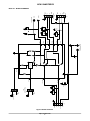
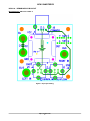
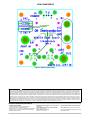
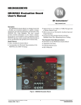
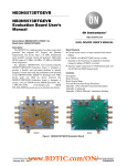
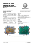
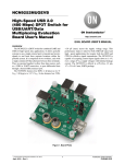
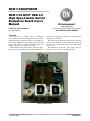
NCN1154MUTGEVB
NCN1154 DP3T USB 2.0
High Speed Audio Switch
Evaluation Board User's
Manual
http://onsemi.com
Prepared by: Bertrand RENAUD
On Semiconductor
EVAL BOARD USER’S MANUAL
OVERVIEW
and provide a safe path to ground for any charge that may
build up on the audio lines.
This reduces Pop & Click noise in the audio system. The
device has an extended VCC range which can operate off
VCC up to 4.2 V while passing true ground audio signals
down to −2 V.
The NCN1154 is housed in a space saving, ultra low
profile 1.7 x 2.0 x 0.5 mm 12 pin DFN package.
The NCN1154 is a DP3T switch for combined
true−ground audio, USB 2.0 high speed data, and UART
applications. It allows portable systems to use a single port
to pass either USB data or audio signals from an external
headset. The switch is capable of passing signals with
negative voltages as low as 2 V below ground.
The NCN1154 features shunt resistors on the audio ports.
These resistors are switched in when the audio channel is off
Figure 1. Board Picture
© Semiconductor Components Industries, LLC, 2010
July, 2010 − Rev. 0
1
Publication Order Number:
EVBUM2003/D
NCN1154MUTGEVB
NCN1154 − BOARD SCHEMATIC
4
3
2
1
“B”
Receptacle J4
VBUS
D−
D+
GND
1
D1
ESD
11n5
1
2
1
2
2
1
ESD
11n5
ESD
11n5
ESD
11n5
1
2
D− (5)
D+ (1)
Rx (4)
Tx (2)
R (6)
L (12)
Banana Jacks
GND
VCC
1uF
Control Logic
VCC (3)
COM− (8)
COM+ (10)
IN1 (11)
0.1uF
ESD
11n5
1
2
ESD
11n5
1
2
VCC
Toggle Switch
SW2
“A”
Receptacle J6
VBUS
D−
D+
GND
http://onsemi.com
“B”
Receptacle J5
VBUS
2
3
D−
4
1
ESD
11n5
2
1
2
VCC
2
D+
GND
right in
left in
Banana Jacks
ESD
11n5
IN2 (7)
Toggle Switch
SW1
Figure 2. Board Schematic
NCN1154MUTGEVB
NCN1154 − BOARD CONNECTIONS
SUPPLY
Symbol
VCC, GND
Description
This is the positive and the return connection for power supply (Pins 3 and 9).
SETUP
Symbol
Description
SW1
This is the toggle switch for IN2 (Pin 7).
SW2
This is the toggle switch for IN1 (Pin 11).
SIGNALS
Symbol
COMMON
USB
UART
Description
This standard USB connector is the common data and audio lines (Pins 8 and 10).
This USB connector Male A type is the high speed USB signaling path (Pins 1 and 5).
This USB connector Male B type is dedicated for Tx and Rx data lines for UART signals (Pins 2 and 4).
LEFT IN
This connector is the left audio signal (Pin 12).
RIGHT IN
This connector is the right audio signal (Pin 6).
http://onsemi.com
3
NCN1154MUTGEVB
NCN1154 − TEST PROCEDURE
Equipment needed
−
−
−
−
−
Power Supply
Digital Ohm Meter
Desktop or Laptop with Windows XP or higher
USB Key
USB Headset
BACKGROUND: IN1 & IN2 TRUTH TABLE
IN1
IN2
D+, D−
Rx, Tx
L, R
L, R SHUNT
0
0
Hi Z
Hi Z
Hi Z
ON
0
1
ON
Hi Z
Hi Z
ON
1
0
Hi Z
Hi Z
ON
OFF
1
1
Hi Z
ON
Hi Z
ON
Test
1. Connect the power supply at 3.6 V from VCC to GND. The supply current should be less than 35 mA.
2. Turn SW1 and SW2 to G (ground) position
The impedance measured from COM+ to D+, Tx and L is over 10 MW.
The impedance measured from COM− to D−, Rx and R is over 10 MW.
The impedance measured from L & R to GND is closed to 118 W.
3. Turn SW1 to + (VCC) and keep SW2 to G (ground)
The impedance measured from COM+ to D+ is closed to 5.5 W.
The impedance measured from COM− to D− is closed to 5.5 W.
The impedance measured from COM+ to Tx and L is over 10 MW.
The impedance measured from COM− to Rx and R is over 10 MW.
The impedance measured from L & R to GND is closed to 118 W.
4. Place a USB key connected to COMMON terminal (J6) and connect the USB terminal (J4) to the laptop or desktop.
The device is being recognized.
Remove both USB cable and USB key for next measurement.
5. Keep SW1 to + (Vcc) and turn SW2 to + (Vcc)
The impedance measured from COM+ to Tx is closed to 5.5 W.
The impedance measured from COM− to Rx is closed to 5.5 W.
The impedance measured from COM+ to D+ and L is over 10 MW.
The impedance measured from COM− to D− and R is over 10 MW.
The impedance measured from L & R to GND is closed to 118 W.
6. Place a USB key connected to COMMON terminal (J6) and connect the UART terminal (J5) to the laptop or desktop.
The device is being recognized.
Remove both USB cable and USB key for next measurement
7. Turn SW1 to G (ground) and keep SW2 to + (Vcc)
The impedance measured from COM+ to L is closed to 3 W.
The impedance measured from COM− to R is closed to 3 W.
The impedance measured from COM+ to D+ and Tx is over 5 MW.
The impedance measured from COM− to D− and Rx is over 5 MW.
The impedance measured from L & R to GND is over 5 MW.
http://onsemi.com
4
NCN1154MUTGEVB
NCN1154 − COMPONENTS SELECTION
Input Capacitor
A 0.1 mF X5R ceramic capacitor or larger must bypass Vcc input to the ground. This capacitor should be placed as close as
possible to this input.
ESD Diode
These devices have limited built−in ESD protection, an external bi−directional ESD / IEC diode is recommended on COM+
and COM− pin. The demoboard includes six additional ESD diodes for test purpose which are not required by the application.
The ESD11N is designed to protect voltage sensitive components that require ultra−low capacitance from ESD and transient
voltage events. Excellent clamping capability, low capacitance, low leakage, and fast response time, make these parts ideal for
ESD protection on designs where board space is at a premium. Because of its low capacitance, it is suited for use in high
frequency designs such as USB 2.0 high speed and antenna line applications.
NCN1154 – BILL OF MATERIAL
Designator
Qty
Description
Value
Tolerance
Footprint
Manufacturer
Manufacturer
Part Number
U1
1
IC, High Speed Switches
NA
NA
UDFN−12
ON Semiconductor
NCN1154
D1, D2, D4, D5, D6, D8,
D10, D12
8
ESD Diode
NA
NA
0.6 x 0.3 mm
ON Semiconductor
ESD11N5.0ST5G
C1, C3
1
Ceramic capacitor
10 nF
$20%
0402
AVX Corporation
04023C103KAT2A
C2
1
Ceramic capacitor
1 mF
$20%
0603
Murata
GRM188R61C105
J6
1
USB Connector Male ANG
Receptable
NA
NA
A Type
Mill−Max
896−43−004−90−000000
J4, J5
2
USB Connector Male
NA
NA
B Type
Molex/Waldom
67265−2001
Single Banana
NA
NA
NA
Pomona Electronics
2142−6
2142−9
VERT Receptable
BJ6
1
BJ12
1
Single Banana
NA
NA
NA
Pomona Electronics
BJ
1
Double Banana
NA
NA
NA
Pomona Electronics
2143−0
SW1, SW2
2
Switch
NA
NA
NA
ITT CANNON
OS103011MS8QP1
PCB
1
5.0 x 5.0 x 0.25 mm
2 Layers
NA
NA
NA
Any
EBT1745−01 REV: A
NCN1154 − PCB LAYOUT GUIDELINES
Electrical Layout Considerations
Implementing a high speed USD device requires paying attention on USB lines and traces to preserve signal integrity. The
demonstration board serves as layout example and can support the design engineers to preserve high speed performances.
Electrical layout guidelines are:
− The bypass capacitor must be placed as close as possible to the Vcc input pin for noise immunity.
− The characteristic impedance of each High Speed USB segment must be 45 W.
− All corresponding D+ / D− line segment pairs must be the same length.
− The use of vias to route these signals should be avoided.
− The use of turns or bends to route these signal should be avoided.
− The ground plane of the PCB will be used to determine the characteristics impedance of each line.
http://onsemi.com
5
NCN1154MUTGEVB
NCN1154 − DEMOBOARD PCB LAYOUT
Board Reference: EBT1745−01 REV: A
Figure 3. Top Layer Routing
http://onsemi.com
6
NCN1154MUTGEVB
Figure 4. Bottom Layer Routing
ON Semiconductor and
are registered trademarks of Semiconductor Components Industries, LLC (SCILLC). SCILLC reserves the right to make changes without further notice
to any products herein. SCILLC makes no warranty, representation or guarantee regarding the suitability of its products for any particular purpose, nor does SCILLC assume any liability
arising out of the application or use of any product or circuit, and specifically disclaims any and all liability, including without limitation special, consequential or incidental damages.
“Typical” parameters which may be provided in SCILLC data sheets and/or specifications can and do vary in different applications and actual performance may vary over time. All
operating parameters, including “Typicals” must be validated for each customer application by customer’s technical experts. SCILLC does not convey any license under its patent rights
nor the rights of others. SCILLC products are not designed, intended, or authorized for use as components in systems intended for surgical implant into the body, or other applications
intended to support or sustain life, or for any other application in which the failure of the SCILLC product could create a situation where personal injury or death may occur. Should
Buyer purchase or use SCILLC products for any such unintended or unauthorized application, Buyer shall indemnify and hold SCILLC and its officers, employees, subsidiaries, affiliates,
and distributors harmless against all claims, costs, damages, and expenses, and reasonable attorney fees arising out of, directly or indirectly, any claim of personal injury or death
associated with such unintended or unauthorized use, even if such claim alleges that SCILLC was negligent regarding the design or manufacture of the part. SCILLC is an Equal
Opportunity/Affirmative Action Employer. This literature is subject to all applicable copyright laws and is not for resale in any manner.
PUBLICATION ORDERING INFORMATION
LITERATURE FULFILLMENT:
Literature Distribution Center for ON Semiconductor
P.O. Box 5163, Denver, Colorado 80217 USA
Phone: 303−675−2175 or 800−344−3860 Toll Free USA/Canada
Fax: 303−675−2176 or 800−344−3867 Toll Free USA/Canada
Email: [email protected]
N. American Technical Support: 800−282−9855 Toll Free
USA/Canada
Europe, Middle East and Africa Technical Support:
Phone: 421 33 790 2910
Japan Customer Focus Center
Phone: 81−3−5773−3850
http://onsemi.com
7
ON Semiconductor Website: www.onsemi.com
Order Literature: http://www.onsemi.com/orderlit
For additional information, please contact your local
Sales Representative
EVBUM2003/D