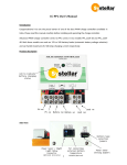
1
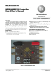
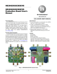
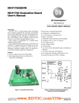
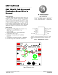
NB4N507ADEVB
NB4N507ADEVB Evaluation
Board User's Manual
http://onsemi.com
Description
EVAL BOARD USER’S MANUAL
The NB4N507ADEVB Evaluation Board provides a
flexible and convenient platform to quickly evaluate,
characterize and verify the performance and operation of the
NB4N507A PECL Clock Synthesizer. This user’s manual
provides detailed information on board contents, layout and
its use. It should be used in conjunction with a device
datasheet: NB4N507A. (www.onsemi.com)
Board Layout
The evaluation board is constructed with Getek material
with 50 W trace impedances and is designed to minimize
noise, achieve high bandwidth and minimize crosstalk.
The NB4N507A evaluation board is equipped with
3−position slide switches. These switches are used to
manipulate the static input logic levels of the Multiplier
Select pins, S0 and S1, and Output Enable pin, OE. The H
position of the slide switch asserts a logic HIGH on the
assigned pin, the L asserts a logic LOW and the M is an open
where the pin “floats” to a mid−logic level by way of the
device’s internal pull−up and pulldown resistors.
Multiplier Select pins, S0 and S1, and Output Enable pin,
OE, also have SMA connector provisions, if the application
requires them.
Board Features
• Accommodates the Electrical Characterization of the
NB4N507A in 16−pin 150 mil SOIC Package
• Supports use of a 10 MHz to 27 MHz Through−hole or
•
•
•
•
•
Surface Mount Crystal
Incorporates on Board Slide Switch Controlled
Multiplier Select and OE Logic Pins, Minimizing
Excess Cabling
SMA Connectors are Provided for Auxiliary Input and
Output Interfaces
Differential PECL Outputs Loaded/Terminated
On−board; Output Signals are Monitored via SMA
Connectors
Convenient and Compact Board Layout
3.3 V or 5.0 V Single or Split−Power Supply Operation
Layer Stack
L1 Signal
L2 SMA Ground
L3 VCC (Positive Power Supply) and DUTGND
(Device Ground, Negative Power Supply)
L4 Signal
Figure 1. Evaluation Board
www.BDTIC.com/ON/
© Semiconductor Components Industries, LLC, 2012
April, 2012 − Rev. 2
1
Publication Order Number:
EVBUM2074/D
NB4N507ADEVB
LAB SETUP PROCEDURE
Power Supply Connections and Output Termination
Use high−impedance probes of the oscilloscope or
frequency counter to monitor the (LV)PECL CLKOUT
outputs.
The NB4N507A has a positive supply pin, VDD, and a
negative supply pin, DUTGND. SMAGND is the ground
plane for the SMA connectors.
Power supply banana plug connectors for VDD,
DUTGND and SMAGND are provided in the corners of the
board. The (LV)PECL CLKOUT outputs have
non−standard, open collector outputs and must be externally
DC loaded and terminated. Thevenin equivalent load and
termination resistors are provided on−board at the output’s
SMA connector.
“Spilt” Power Supply (Optional)
For some tests, an optional “split” or dual power supply
technique can be used, however, doing so will double
terminate the (LV)PECL outputs into 50 Ws of an
oscilloscope or a frequency counter, and will therefore,
appear to halve the output amplitude. Since VTT = VDD –
2.0 V, off setting VDD by +2.0 V yields VTT = 0 V or
Ground. The VTT terminal connects to the isolated
SMAGND connector ground plane, and is not to be
confused with the device ground pin or DUTGND.
Single Supply (Recommended)
Connect a single power supply to the evaluation board.
(see Figure 2); Connect VDD to +3.3 V, Connect GND to
0 V.
Table 1. POWER SUPPLY CONFIGURATIONS
Device Pin
Power Supply
Single Supply
“Spilt” Power Supply (Optional)
VDD
RED
+3.3 V or +5.0 V
VDD = +2.0 V
SMAGND
BLACK
0V
VTT = VDD – 2.0 V = 0 V
DUTGND
BLACK
0V
DUTGND = −1.3 V (or –3.0 V)
Dual Power Supplies
Power Supplies
+3.3 V
+
+2.0 V
−
+
VCC
GND
VDD
+1.3 V
−
+
−
VTT
GND
+3.3 V
+3.3 V
Figure 3. “Split” Power Supply Connections
Figure 2. Single Power Supply Configuration
www.BDTIC.com/ON/
http://onsemi.com
2
NB4N507ADEVB
Open Traces (Intentional)
For Crystal Use
SMAGND
VDD
Signal Generator
OUT
10 MHz to 133 MHz
50 W
(Optional)
DUTGND
Real Time, Digital Oscilloscope,
or Frequency Counter
PECL Output
Load/Termination
Resistors
CLKOUT
CLKOUT
Hi−Z or 50 W
Trigger
Hi−Z or 50 W
Figure 4. NB4N507A Evaluation Board
LAB SETUP AND MEASUREMENT PROCEDURE
Equipment Used
a.. Connect a single power supply to the evaluation
board. (see Figure 2)
Connect VDD to +3.3 V
Connect GND to 0 V
b.. or; Connect a “split” power supply to the
evaluation board. (see Figure 3)
Connect VCC banana jack to +2.0 V
Connect VTT banana jack to
SMA_GND= 0 V
Connect GND banana jack to −1.3 V for
3.3 V operation, or −3.0 V for 5.0 V operation
2. Determine if a crystal or an external clock
reference will be used.
a.. For crystal use, install a crystal
• Agilent Signal Generator #33250A for CLK, External
Clock Source
• Tektronix or LeCroy with High Impedance Probes or
TDS8000 Oscilloscope or Frequency Counter
• Agilent #6624A DC Power Supply
• Digital Voltmeter
• Matched High−speed Cables with SMA Connectors for
the PECL CLKOUT Pins
In order to get started and demonstrate the NB4N507A,
perform the following test setup sequence:
1. To monitor the CLKOUT outputs on an
oscilloscope or frequency counter;
www.BDTIC.com/ON/
http://onsemi.com
3
NB4N507ADEVB
5.
b.. For external clock reference use, short the open
trace at Pin 1 and provide an external clock
reference from a signal generator
(10 − 27 MHz) into the X1/CLK pin. Terminate
the signal generator with 50 W to SMA ground.
3. Set the programmable S0 and S1 pin switches
accordingly to achieve the desired function table
logic input levels.
4. Set the OE pin to a logic HIGH
a.. If a single power supply is used, connect the
CLKOUT outputs to the oscilloscope with
matched high−impedance probe cables.
b.. If a split power supply is used, connect the
CLKOUT outputs to the oscilloscope with
matched cables.
6. Ensure the oscilloscope is triggered properly.
Trigger the oscilloscope from the CLKOUT
output.
NB4N507A EVALUATION BOARD PIN DESCRIPTIONS AND FEATURES BY PIN
The H position of the DIP switch asserts a logic HIGH
(VCC) on the assigned pin and the L asserts a logic LOW
(DUTGND). The S0 and S1 device pins have internal
pull−up and pulldown resistors. When left open, the S0 or S1
switch “floats” to mid−logic level. In the M position, the
slide switch is an open and the pin “floats” to the mid−logic
level.
The NB4N507A Evaluation Board was designed to
accommodate the test and evaluation of the NB4N507A
PECL Clock Synthesizer. Detailed board features by device
pin are described below:
Crystal (X1/CLK and X2)
A through−hole or surface mount crystal can be used. The
metal traces at the crystal pins are intentionally open for
crystal use and will have no impedance affect on the crystal
pins.
CLKOUT and CLKOUT
The CLKOUT and CLKOUT PECL outputs have equal
length, 50 W board traces with SMA connectors. Matched
cables can connect to an oscilloscope or frequency counter.
The (LV)PECL CLKOUT outputs have nonstandard,
open collector outputs and must be externally DC loaded and
terminated.
Thevenin equivalent load and termination resistors are
provided on board at the output’s SMA connector.
X1/CLK − External Clock
An SMA connector is provided for X1/CLK if an external
clock source is used on Pin 1. The metal trace at the package
pin is intentionally open for crystal use, but, must be shorted
for a connection to Pin 1 for external clock use. The unused
component pad labeled C2 (used for the crystal load
capacitor) may be used for a 50 W resistor to ground to
terminate an external signal generator.
OE
The Output Enable function can be exercised manually
with the OE switch when the JMP4 jumper is used, or they
can be controlled externally via the SMA connector and the
jumper open.
S0 and S1
The S0 and S1 multiplier select pins can be exercised
manually with the S0 and S1 slide switches when the
jumpers are used across JMP2 and JMP5, or they can be
controlled externally via the SMA connectors with the
jumpers open.
www.BDTIC.com/ON/
http://onsemi.com
4
NB4N507ADEVB
Figure 5. Evaluation Board Schematic
www.BDTIC.com/ON/
http://onsemi.com
5
NB4N507ADEVB
Table 2. NB4N507A DEMO / EVALUATION BOARD BILL OF MATERIALS
Value
Qty
BANANA1
Reference Designators
Connector, Banana Jack, Deltron, Mouser #164−6219
Description
RED
1
BANANA2, BANANA3
Connector, Banana Jack, Deltron, Mouser #164−6218
BLACK
2
C3, C7, C10, C12
Cap, Chip, 0.010 mF, 0805, 50 V, 10%
0.01 mF
4
C4, C6, C8, C11
Cap, Chip, 0.1 mF, 0805, 50 V, 10%
0.1 mF
4
C5, C9
Cap, Chip, 22 mF, Tant ”C”, 16 V, 10%
22 mF
2
C13
Cap, Chip, 22 mF, 1210, 10 V, Y5V
22 mF
1
J1, J2, J3, J4, J5, J6, J7
Connector, SMA, Edge Mount, Johnson #142−0711−821
JMP2, JMP4, JMP5
Header, Male, Square, Single Row, 40 Pin
2 Pins
3
R1, R4
Resistor, Chip, 62 W, 0603, 1/10 W, 1%
62 W
2
R2, R3
Resistor, Chip, 270 W, 0603, 1/16 W 1%
270 W
2
R5, R8, R9
Not applicable
−
−
R7
Resistor, Chip, 0 W, 0805, 1/8 W, 5%
0W
1
SW1, SW2, SW3
Switch, C&K, 3 Position, Miniature, #OS103011MS8QP1
Y1
Crystal, ABRACON #ABL−25.000MHZ−B2F (Through−Hole)
CTS FREQ . #ATS 250 BSM−1E (Surface Mount)
CTS FREQ. #ATS 250 B−3 (Through−Hole)
Y1 (for Through−hole Xtal)
Pin Receptacle, Ampere, .140 lg, Maximum Pin 0.021 Tin, Gold
7
3
25 MHz
1
2
ON Semiconductor and
are registered trademarks of Semiconductor Components Industries, LLC (SCILLC). SCILLC reserves the right to make changes without further notice
to any products herein. SCILLC makes no warranty, representation or guarantee regarding the suitability of its products for any particular purpose, nor does SCILLC assume any liability
arising out of the application or use of any product or circuit, and specifically disclaims any and all liability, including without limitation special, consequential or incidental damages.
“Typical” parameters which may be provided in SCILLC data sheets and/or specifications can and do vary in different applications and actual performance may vary over time. All
operating parameters, including “Typicals” must be validated for each customer application by customer’s technical experts. SCILLC does not convey any license under its patent rights
nor the rights of others. SCILLC products are not designed, intended, or authorized for use as components in systems intended for surgical implant into the body, or other applications
intended to support or sustain life, or for any other application in which the failure of the SCILLC product could create a situation where personal injury or death may occur. Should
Buyer purchase or use SCILLC products for any such unintended or unauthorized application, Buyer shall indemnify and hold SCILLC and its officers, employees, subsidiaries, affiliates,
and distributors harmless against all claims, costs, damages, and expenses, and reasonable attorney fees arising out of, directly or indirectly, any claim of personal injury or death
associated with such unintended or unauthorized use, even if such claim alleges that SCILLC was negligent regarding the design or manufacture of the part. SCILLC is an Equal
Opportunity/Affirmative Action Employer. This literature is subject to all applicable copyright laws and is not for resale in any manner.
PUBLICATION ORDERING INFORMATION
LITERATURE FULFILLMENT:
Literature Distribution Center for ON Semiconductor
P.O. Box 5163, Denver, Colorado 80217 USA
Phone: 303−675−2175 or 800−344−3860 Toll Free USA/Canada
Fax: 303−675−2176 or 800−344−3867 Toll Free USA/Canada
Email: [email protected]
N. American Technical Support: 800−282−9855 Toll Free
USA/Canada
Europe, Middle East and Africa Technical Support:
Phone: 421 33 790 2910
Japan Customer Focus Center
Phone: 81−3−5817−1050
ON Semiconductor Website: www.onsemi.com
Order Literature: http://www.onsemi.com/orderlit
For additional information, please contact your local
Sales Representative
www.BDTIC.com/ON/
http://onsemi.com
6
EVBUM2074/D