1
SERIES IP340 and IP341 INDUSTRIAL I/O PACK
SIMULTANEOUS SAMPLE AND HOLD MODULES
___________________________________________________________________________________________
1. The IP model number is represented by a two-digit code
within the ID space (for example the IP340 is represented by
28 Hex IP model code).
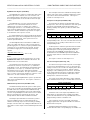
This read/write register is used to: enable single or
continuous conversions, select conversion of calibration voltages
or field analog signals, control external trigger input/output mode,
enable/disable interrupts, monitor FIFO status, and issue a
software reset to the module.
I/O SPACE ADDRESS MAP
This board is addressable in the Industrial Pack I/O space to
control the conversion of analog inputs from the field. As such,
three types of information are stored in the I/O space: control,
status, and data.
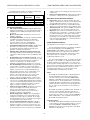
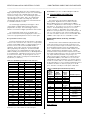
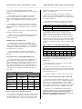
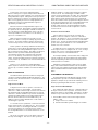
Table 3.3: Channel Control/Status Register
BIT
FUNCTION
00 = Conversions are disabled.
1, 0
01 = Enable Single Conversion Mode. A single
conversion is initiated per software start convert
or external trigger. The internal channel timer
controls the start conversion of channels 8-15.
10 = Enable Continuous Conversion Mode.
Conversions are initiated by a software start
convert or external trigger and continued by
internal hardware triggers generated at the
frequency set by the interval timer registers.
11 = Reserved
00 = All Channels Differential Input.
3, 2
01 = Auto Zero Calibration Voltage Input.
10 = Auto Span Calibration Voltage.
11 = Reserved
00 = External Trigger Disable.
5, 4
01 = External Trigger Set as Input.
10 = External Trigger Set as Output.
11 = Reserved.
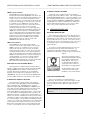
As an output Internal Timer triggers are
driven on the External trigger pin of the field I/O
connector. The External Trigger output signal
can be used to synchronize the conversion of
multiple modules. A single master IP340 or
IP341 must be selected for External Trigger
output and Continuous Conversion mode while
all other modules are selected for External
Trigger input and Single Conversion mode. The
external trigger signals (pin 49 of the field I/O)
must be wired together for all synchronized
modules. Also, the High Bank Timer must be
programmed with the same value on all
synchronized modules.
The External Trigger input can be sensitive
to external EMI noise which can cause
erroneous external triggers. If External Trigger
Input or output is not required, the External
Trigger should be configured as Disabled.
6
0 = Disable Interrupt
1 = Enable Interrupt
If enabled via this bit an interrupt request from
the module will be issued to the system if the
FIFO contains more than the threshold number
of bytes selected via the threshold register.
The interrupt request will remain active until the
interrupt condition is removed, or by disabling
interrupts via this bit. The interrupt condition
can be removed by reading the channel data
from the FIFO buffer (thus reducing the number
of samples below the set threshold).
7
Not Used
8
0 = FIFO Empty
1 = FIFO Not Empty
Status
9
0 = FIFO has less than or equal number of samples
Status
as defined by the threshold register.
1 = FIFO Threshold Reached.
This bit is set when the FIFO contains more
than the number of data samples set by the
threshold register.
10
0 = FIFO Not Full
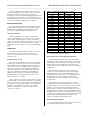
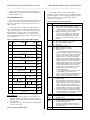
The I/O space may be as large as 64, 16-bit words (128
bytes) using address lines A1 to A6, but the IP340/IP341 uses
only a portion of this space. The I/O space address map for the
IP340 and IP341 is shown in Table 3.2. Note that the base
address for the IP module I/O space (see your carrier board
instructions) must be added to the addresses shown to properly
access the I/O space.
Table 3.2: IP340/IP341 I/O Space Address Memory Map2
Hex
MSB
LSB
Hex
Base D15
D08 D07
D00 Base
Adr+
Adr+
00
Control Register
01
02
Channel Enable Control
03
04
Conversion Timer
Bits 15 to 0
05
06
Not Used
Conversion Timer
07
Bits-15 to 08
Bits 23 to 16
08
High Bank Timer
09
Bits 15 to 0
0A
High Bank Timer
0B
Bits 23 to 16
0C
FIFO Full Interrupt Threshold
0D
0E
Not Used
Interrupt Vector
0F
Bits-15 to 08
10
Not Used
Start
Bits-15 to 01
Convert 11
12
FIFO Channel Data Port
13
14
FIFO Data Tag
15
Port
16
Rd
Address
Reference Voltage
17
Wr~
Port
Write Data Port
18
Reference Voltage
Wr
Rd
Read Data Port
Busy
Comp 19
1A
Reserved3
Not Used1
1B
1C
Not Used1
1D
⇓
7E
Not Used1
7F
Notes (Table 3.2):
1. The IP will not respond to addresses that are "Not Used".
2. All Reads and writes are 0 wait states (except read from
FIFO ports which require 2 wait states worst case and 0 wait
states typically).
3. This byte is reserved for use at the factory to enable writing
of the reference voltage.
Control Register (Read/Write, 00H)
-7-