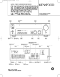
1
Order this document by
DSP563XXEVMEUM
Rev. 0.3, 09/2007
DSP563XXEVME User’s Manual
Freescale Semiconductor
6501 William Cannon Drive West
Austin TX 78735-8598
How to Reach Us:
Home Page:
www.freescale.com
Web Support:
http://www.freescale.com/support
USA/Europe or Locations Not Listed:
Freescale Semiconductor, Inc.
Technical Information Center, EL516
2100 East Elliot Road
Tempe, Arizona 85284
+1-800-521-6274 or +1-480-768-2130
www.freescale.com/support
Europe, Middle East, and Africa:
Freescale Halbleiter Deutschland GmbH
Technical Information Center
Schatzbogen 7
81829 Muenchen, Germany
+44 1296 380 456 (English)
+46 8 52200080 (English)
+49 89 92103 559 (German)
+33 1 69 35 48 48 (French)
www.freescale.com/support
Japan:
Freescale Semiconductor Japan Ltd.
Headquarters
ARCO Tower 15F
1-8-1, Shimo-Meguro, Meguro-ku,
Tokyo 153-0064
Japan
0120 191014 or +81 3 5437 9125
[email protected]
Asia/Pacific:
Freescale Semiconductor Hong Kong Ltd.
Technical Information Center
2 Dai King Street
Tai Po Industrial Estate
Tai Po, N.T., Hong Kong
+800 2666 8080
[email protected]
For Literature Requests Only:
Freescale Semiconductor Literature Distribution Center
P.O. Box 5405
Denver, Colorado 80217
1-800-441-2447 or 303-675-2140
Fax: 303-675-2150
[email protected]
Document Number: DSP563XXEVMEUM
Rev. 0.3
09/2007
Information in this document is provided solely to enable system and software
implementers to use Freescale Semiconductor products. There are no express or
implied copyright licenses granted hereunder to design or fabricate any integrated
circuits or integrated circuits based on the information in this document.
Freescale Semiconductor reserves the right to make changes without further notice to
any products herein. Freescale Semiconductor makes no warranty, representation or
guarantee regarding the suitability of its products for any particular purpose, nor does
Freescale Semiconductor assume any liability arising out of the application or use of any
product or circuit, and specifically disclaims any and all liability, including without
limitation consequential or incidental damages. “Typical” parameters that may be
provided in Freescale Semiconductor data sheets and/or specifications can and do vary
in different applications and actual performance may vary over time. All operating
parameters, including “Typicals”, must be validated for each customer application by
customer’s technical experts. Freescale Semiconductor does not convey any license
under its patent rights nor the rights of others. Freescale Semiconductor products are
not designed, intended, or authorized for use as components in systems intended for
surgical implant into the body, or other applications intended to support or sustain life,
or for any other application in which the failure of the Freescale Semiconductor product
could create a situation where personal injury or death may occur. Should Buyer
purchase or use Freescale Semiconductor products for any such unintended or
unauthorized application, Buyer shall indemnify and hold Freescale Semiconductor and
its officers, employees, subsidiaries, affiliates, and distributors harmless against all
claims, costs, damages, and expenses, and reasonable attorney fees arising out of,
directly or indirectly, any claim of personal injury or death associated with such
unintended or unauthorized use, even if such claim alleges that Freescale
Semiconductor was negligent regarding the design or manufacture of the part.
RoHS-compliant and/or Pb-free versions of Freescale products have the functionality
and electrical characteristics as their non-RoHS-compliant and/or non-Pb-free
counterparts. For further information, see http://www.freescale.com or contact your
Freescale sales representative.
For information on Freescale’s Environmental Products program, go to
http://www.freescale.com/epp.
Freescale™ and the Freescale logo are trademarks of Freescale Semiconductor, Inc.
All other product or service names are the property of their respective owners.
© Freescale Semiconductor, Inc. 2007. All rights reserved.
Table of Contents
Chapter 1
Quick Start Guide
1.1
1.1.1
1.1.2
1.2
1.2.1
1.2.2
1.2.3
1.2.4
1.2.5
1.3
1.4
Equipment . . . . . . . . . . . . . . . . . . . . . . . . . . . . . . . . . . . . . . . . . . . . . . . . . . . . . .
What You Get with the DSP563XXEVME . . . . . . . . . . . . . . . . . . . . . . . . . .
What You Need to Supply . . . . . . . . . . . . . . . . . . . . . . . . . . . . . . . . . . . . . . .
Installation Procedure . . . . . . . . . . . . . . . . . . . . . . . . . . . . . . . . . . . . . . . . . . . . .
Installing the Desired DSP . . . . . . . . . . . . . . . . . . . . . . . . . . . . . . . . . . . . . . .
Verifying Settings for Jumpers, Switches . . . . . . . . . . . . . . . . . . . . . . . . . . .
Connecting the Board to the PC and Power . . . . . . . . . . . . . . . . . . . . . . . . . .
Installing the Software . . . . . . . . . . . . . . . . . . . . . . . . . . . . . . . . . . . . . . . . . .
Troubleshooting . . . . . . . . . . . . . . . . . . . . . . . . . . . . . . . . . . . . . . . . . . . . . . .
Additional Information . . . . . . . . . . . . . . . . . . . . . . . . . . . . . . . . . . . . . . . . . . . .
Factory Test . . . . . . . . . . . . . . . . . . . . . . . . . . . . . . . . . . . . . . . . . . . . . . . . . . . . .
1-1
1-1
1-2
1-2
1-4
1-4
1-6
1-7
1-7
1-8
1-8
Chapter 2
DSP563XXEVME Technical Summary
2.1
DSP563XXEVME Description and Features . . . . . . . . . . . . . . . . . . . . . . . . . . . 2-1
2.2
DSP56300 Family Description . . . . . . . . . . . . . . . . . . . . . . . . . . . . . . . . . . . . . . 2-1
2.3
Component Layout. . . . . . . . . . . . . . . . . . . . . . . . . . . . . . . . . . . . . . . . . . . . . . . . 2-2
2.4
Memory . . . . . . . . . . . . . . . . . . . . . . . . . . . . . . . . . . . . . . . . . . . . . . . . . . . . . . . . 2-2
2.4.1
FSRAM. . . . . . . . . . . . . . . . . . . . . . . . . . . . . . . . . . . . . . . . . . . . . . . . . . . . . . 2-2
2.4.1.1
FSRAM Connections . . . . . . . . . . . . . . . . . . . . . . . . . . . . . . . . . . . . . . . . 2-3
2.4.1.2
Example: Programming AAR0. . . . . . . . . . . . . . . . . . . . . . . . . . . . . . . . . 2-3
2.4.2
Flash . . . . . . . . . . . . . . . . . . . . . . . . . . . . . . . . . . . . . . . . . . . . . . . . . . . . . . . . 2-5
2.4.2.1
Flash Connections . . . . . . . . . . . . . . . . . . . . . . . . . . . . . . . . . . . . . . . . . . . 2-6
2.4.2.2
Programming for Stand-Alone Operation. . . . . . . . . . . . . . . . . . . . . . . . . 2-6
2.4.2.3
Flash Programming Example . . . . . . . . . . . . . . . . . . . . . . . . . . . . . . . . . . 2-6
2.5
Audio Codec . . . . . . . . . . . . . . . . . . . . . . . . . . . . . . . . . . . . . . . . . . . . . . . . . . . . 2-7
2.5.1
Codec Analog Input/Output . . . . . . . . . . . . . . . . . . . . . . . . . . . . . . . . . . . . . . 2-7
2.5.2
Codec Digital Interface. . . . . . . . . . . . . . . . . . . . . . . . . . . . . . . . . . . . . . . . . . 2-8
2.6
JTAG Header . . . . . . . . . . . . . . . . . . . . . . . . . . . . . . . . . . . . . . . . . . . . . . . . . . . . 2-9
2.7
Off-Board Interfaces . . . . . . . . . . . . . . . . . . . . . . . . . . . . . . . . . . . . . . . . . . . . . 2-10
2.7.1
Serial Communication Interface Port (SCI) . . . . . . . . . . . . . . . . . . . . . . . . . 2-10
Freescale Semiconductor
DSP563XXEVME User’s Manual, Rev. 0.3
iii
2.7.2
Enhanced Synchronous Serial Port 0 (ESSI0). . . . . . . . . . . . . . . . . . . . . . . . 2-11
2.7.3
Enhanced Synchronous Serial Port 1 (ESSI1). . . . . . . . . . . . . . . . . . . . . . . . 2-12
2.7.4
Host Port (HI08) . . . . . . . . . . . . . . . . . . . . . . . . . . . . . . . . . . . . . . . . . . . . . . 2-12
2.7.5
External Bus Control . . . . . . . . . . . . . . . . . . . . . . . . . . . . . . . . . . . . . . . . . . . 2-13
2.8
Reset, IRQ, and Mode Selection Switches . . . . . . . . . . . . . . . . . . . . . . . . . . . . . 2-13
2.8.1
Reset (SW1). . . . . . . . . . . . . . . . . . . . . . . . . . . . . . . . . . . . . . . . . . . . . . . . . . 2-13
2.8.2
IRQ_A and IRQ_D (SW2, SW3) . . . . . . . . . . . . . . . . . . . . . . . . . . . . . . . . . 2-13
2.8.3
Mode Selection Switches (SW4) . . . . . . . . . . . . . . . . . . . . . . . . . . . . . . . . . . 2-13
2.9
LEDs . . . . . . . . . . . . . . . . . . . . . . . . . . . . . . . . . . . . . . . . . . . . . . . . . . . . . . . . . . 2-14
Chapter 3
Example Test Program
3.1
Writing the Program . . . . . . . . . . . . . . . . . . . . . . . . . . . . . . . . . . . . . . . . . . . . . . . 3-2
3.1.1
Source Statement Format. . . . . . . . . . . . . . . . . . . . . . . . . . . . . . . . . . . . . . . . . 3-2
3.1.1.1
Label Field . . . . . . . . . . . . . . . . . . . . . . . . . . . . . . . . . . . . . . . . . . . . . . . . . 3-3
3.1.1.2
Operation Field . . . . . . . . . . . . . . . . . . . . . . . . . . . . . . . . . . . . . . . . . . . . . 3-3
3.1.1.3
Operand Field. . . . . . . . . . . . . . . . . . . . . . . . . . . . . . . . . . . . . . . . . . . . . . . 3-3
3.1.1.4
Data Transfer Fields. . . . . . . . . . . . . . . . . . . . . . . . . . . . . . . . . . . . . . . . . . 3-3
3.1.1.5
Comment Field. . . . . . . . . . . . . . . . . . . . . . . . . . . . . . . . . . . . . . . . . . . . . . 3-4
3.1.2
Example Program . . . . . . . . . . . . . . . . . . . . . . . . . . . . . . . . . . . . . . . . . . . . . . 3-4
3.2
Assembling the Program . . . . . . . . . . . . . . . . . . . . . . . . . . . . . . . . . . . . . . . . . . . . 3-5
3.2.1
Assembler Command Format . . . . . . . . . . . . . . . . . . . . . . . . . . . . . . . . . . . . . 3-5
3.2.2
Assembler Options . . . . . . . . . . . . . . . . . . . . . . . . . . . . . . . . . . . . . . . . . . . . . 3-6
3.2.3
Assembler Directives. . . . . . . . . . . . . . . . . . . . . . . . . . . . . . . . . . . . . . . . . . . . 3-8
3.2.3.1
Assembler Significant Characters . . . . . . . . . . . . . . . . . . . . . . . . . . . . . . . 3-8
3.2.3.2
Assembly Control . . . . . . . . . . . . . . . . . . . . . . . . . . . . . . . . . . . . . . . . . . . 3-9
3.2.3.3
Symbol Definition . . . . . . . . . . . . . . . . . . . . . . . . . . . . . . . . . . . . . . . . . . . 3-9
3.2.3.4
Data Definition/Storage Allocation . . . . . . . . . . . . . . . . . . . . . . . . . . . . . 3-10
3.2.3.5
Listing Control and Options. . . . . . . . . . . . . . . . . . . . . . . . . . . . . . . . . . . 3-10
3.2.3.6
Object File Control. . . . . . . . . . . . . . . . . . . . . . . . . . . . . . . . . . . . . . . . . . 3-10
3.2.3.7
Macros and Conditional Assembly . . . . . . . . . . . . . . . . . . . . . . . . . . . . . 3-11
3.2.3.8
Structured Programming . . . . . . . . . . . . . . . . . . . . . . . . . . . . . . . . . . . . . 3-11
3.2.4
Assembling the Example Program . . . . . . . . . . . . . . . . . . . . . . . . . . . . . . . . 3-11
3.3
DSP Linker . . . . . . . . . . . . . . . . . . . . . . . . . . . . . . . . . . . . . . . . . . . . . . . . . . . . . 3-12
3.4
Linker Options . . . . . . . . . . . . . . . . . . . . . . . . . . . . . . . . . . . . . . . . . . . . . . . . . . 3-12
3.4.1
Linker Directives . . . . . . . . . . . . . . . . . . . . . . . . . . . . . . . . . . . . . . . . . . . . . . 3-17
3.5
Introduction to the Debugger Software. . . . . . . . . . . . . . . . . . . . . . . . . . . . . . . . 3-17
iv
DSP563XXEVME User’s Manual, Rev. 0.3
Freescale Semiconductor
3.6
Running the Program . . . . . . . . . . . . . . . . . . . . . . . . . . . . . . . . . . . . . . . . . . . . . 3-18
Appendix A
Codec Programming Example
A.1
A.2
A.2.1
A.2.2
A.3
A.4
A.5
A.5.1
A.5.2
A.5.3
A.5.4
A.6
A.7
A.8
A.8.1
A.8.2
A.8.3
A.8.4
A.8.5
A.9
A.10
Introduction . . . . . . . . . . . . . . . . . . . . . . . . . . . . . . . . . . . . . . . . . . . . . . . . . . . . . 4-1
Codec Background . . . . . . . . . . . . . . . . . . . . . . . . . . . . . . . . . . . . . . . . . . . . . . . . 4-1
Codec Device . . . . . . . . . . . . . . . . . . . . . . . . . . . . . . . . . . . . . . . . . . . . . . . . . 4-1
Codec Modes . . . . . . . . . . . . . . . . . . . . . . . . . . . . . . . . . . . . . . . . . . . . . . . . . 4-1
ESSI Ports Background . . . . . . . . . . . . . . . . . . . . . . . . . . . . . . . . . . . . . . . . . . . . 4-3
ESSI/GPIO pins . . . . . . . . . . . . . . . . . . . . . . . . . . . . . . . . . . . . . . . . . . . . . . . . . . 4-4
ESSI Port Registers . . . . . . . . . . . . . . . . . . . . . . . . . . . . . . . . . . . . . . . . . . . . . . . 4-4
ESSI/GPIO Shared Registers . . . . . . . . . . . . . . . . . . . . . . . . . . . . . . . . . . . . . 4-4
ESSI Registers . . . . . . . . . . . . . . . . . . . . . . . . . . . . . . . . . . . . . . . . . . . . . . . . 4-5
GPIO Registers . . . . . . . . . . . . . . . . . . . . . . . . . . . . . . . . . . . . . . . . . . . . . . . . 4-5
GPIO Mode Port C and Port D. . . . . . . . . . . . . . . . . . . . . . . . . . . . . . . . . . . . 4-6
Digital Interface (ESSI – Codec) . . . . . . . . . . . . . . . . . . . . . . . . . . . . . . . . . . . . . 4-6
Programming the CS4270 Codec. . . . . . . . . . . . . . . . . . . . . . . . . . . . . . . . . . . . . 4-9
Initializing the ESSI and Codec . . . . . . . . . . . . . . . . . . . . . . . . . . . . . . . . . . . . . . 4-9
Configuring IO Pins . . . . . . . . . . . . . . . . . . . . . . . . . . . . . . . . . . . . . . . . . . . . 4-9
Resetting Codec . . . . . . . . . . . . . . . . . . . . . . . . . . . . . . . . . . . . . . . . . . . . . . 4-12
Communicating with Codec Control Port . . . . . . . . . . . . . . . . . . . . . . . . . . 4-13
Power Control and Configuration of Codec . . . . . . . . . . . . . . . . . . . . . . . . . 4-15
Configuring for ESSI0 . . . . . . . . . . . . . . . . . . . . . . . . . . . . . . . . . . . . . . . . . 4-16
Example Code Files . . . . . . . . . . . . . . . . . . . . . . . . . . . . . . . . . . . . . . . . . . . . . . 4-18
Data Transfer Mechanism . . . . . . . . . . . . . . . . . . . . . . . . . . . . . . . . . . . . . . . . . 4-19
Freescale Semiconductor
DSP563XXEVME User’s Manual, Rev. 0.3
v
vi
DSP563XXEVME User’s Manual, Rev. 0.3
Freescale Semiconductor
List of Tables
1-1
Jumper Settings . . . . . . . . . . . . . . . . . . . . . . . . . . . . . . . . . . . . . . . . . . . . . 1-5
2-1
J2 Jumper Block Options . . . . . . . . . . . . . . . . . . . . . . . . . . . . . . . . . . . . . 2-9
2-2
J6 Jumper Block Options . . . . . . . . . . . . . . . . . . . . . . . . . . . . . . . . . . . . . 2-9
2-3
JTAG/OnCE (J3) Connector Pinout . . . . . . . . . . . . . . . . . . . . . . . . . . . . 2-10
2-4
SCI Header (J9) Pinout . . . . . . . . . . . . . . . . . . . . . . . . . . . . . . . . . . . . . . 2-10
2-5
J9 Jumper Options. . . . . . . . . . . . . . . . . . . . . . . . . . . . . . . . . . . . . . . . . . 2-11
2-6
ESSI0 Header (J2) Pinout . . . . . . . . . . . . . . . . . . . . . . . . . . . . . . . . . . . . 2-11
2-7
ESSI0 Header (J6) Pinout . . . . . . . . . . . . . . . . . . . . . . . . . . . . . . . . . . . . 2-12
2-8
HI08 Header (J11) Pinout . . . . . . . . . . . . . . . . . . . . . . . . . . . . . . . . . . . . 2-12
2-9
External Bus Control Signal Header (J17) Pinout . . . . . . . . . . . . . . . . . 2-13
2-10
Boot Mode Selection Options . . . . . . . . . . . . . . . . . . . . . . . . . . . . . . . . . 2-14
2-11
LED Timer Pins . . . . . . . . . . . . . . . . . . . . . . . . . . . . . . . . . . . . . . . . . . . 2-14
3-1
Assembler Options . . . . . . . . . . . . . . . . . . . . . . . . . . . . . . . . . . . . . . . . . . 3-6
3-2
Linker Options . . . . . . . . . . . . . . . . . . . . . . . . . . . . . . . . . . . . . . . . . . . . 3-13
A-1
ESSI Pin Definition. . . . . . . . . . . . . . . . . . . . . . . . . . . . . . . . . . . . . . . . . . 4-4
A-2
ESSI/GPIO Shared Registers . . . . . . . . . . . . . . . . . . . . . . . . . . . . . . . . . . 4-4
A-3
ESSI Registers . . . . . . . . . . . . . . . . . . . . . . . . . . . . . . . . . . . . . . . . . . . . . 4-5
A-4
GPIO Registers . . . . . . . . . . . . . . . . . . . . . . . . . . . . . . . . . . . . . . . . . . . . . 4-5
A-5
Pin Set-Up Descriptions . . . . . . . . . . . . . . . . . . . . . . . . . . . . . . . . . . . . . . 4-7
A-6
J2 Jumper Block (ESSI0) . . . . . . . . . . . . . . . . . . . . . . . . . . . . . . . . . . . . . 4-7
A-7
J6 Jumper Block (ESSI1) . . . . . . . . . . . . . . . . . . . . . . . . . . . . . . . . . . . . . 4-8
A-8
Port Data Register C Pin/bit Correspondence. . . . . . . . . . . . . . . . . . . . . 4-10
A-9
Port Data Register D Pin/bit Correspondence . . . . . . . . . . . . . . . . . . . . 4-10
A-10
Data Direction Register C . . . . . . . . . . . . . . . . . . . . . . . . . . . . . . . . . . . . 4-11
A-11
Data Direction Register D. . . . . . . . . . . . . . . . . . . . . . . . . . . . . . . . . . . . 4-12
A-12
Settings for Control Register A. . . . . . . . . . . . . . . . . . . . . . . . . . . . . . . . 4-16
A-13
Settings Control Register B . . . . . . . . . . . . . . . . . . . . . . . . . . . . . . . . . . 4-17
Freescale Semiconductor
DSP563XXEVME User’s Manual, Rev. 0.3
vii
viii
DSP563XXEVME User’s Manual, Rev. 0.3
Freescale Semiconductor
List of Figures
1-1
DSP563XXEVME Component Layout . . . . . . . . . . . . . . . . . . . . . . . . . . 1-6
2-1
DSP563XXEVME Component Layout . . . . . . . . . . . . . . . . . . . . . . . . . . 2-2
2-2
FSRAM Connections to the DSP . . . . . . . . . . . . . . . . . . . . . . . . . . . . . . . 2-3
2-3
Example Memory Map with the Unified External Memory. . . . . . . . . . . 2-4
2-4
Address Attribute Register AAR0 . . . . . . . . . . . . . . . . . . . . . . . . . . . . . . 2-5
2-5
Flash Connections . . . . . . . . . . . . . . . . . . . . . . . . . . . . . . . . . . . . . . . . . . . 2-6
2-6
Codec Analog Input/Output Diagram . . . . . . . . . . . . . . . . . . . . . . . . . . . . 2-7
2-7
Codec Digital Interface Connections . . . . . . . . . . . . . . . . . . . . . . . . . . . . 2-8
3-1
Development Process Flow. . . . . . . . . . . . . . . . . . . . . . . . . . . . . . . . . . . . 3-2
3-2
Example Debugger Window Display . . . . . . . . . . . . . . . . . . . . . . . . . . . 3-18
3-3
Additional Debugger Windows . . . . . . . . . . . . . . . . . . . . . . . . . . . . . . . 3-19
A-1
Data Format of Codec . . . . . . . . . . . . . . . . . . . . . . . . . . . . . . . . . . . . . . . . 4-3
A-2
ESSI/Codec Pin Diagram . . . . . . . . . . . . . . . . . . . . . . . . . . . . . . . . . . . . . 4-8
Freescale Semiconductor
DSP563XXEVME User’s Manual, Rev. 0.3
ix
x
DSP563XXEVME User’s Manual, Rev. 0.3
Freescale Semiconductor
List of Examples
3-1
Example Source Statement . . . . . . . . . . . . . . . . . . . . . . . . . . . . . . . . . . . . 3-3
3 -2
Simple DSP56303 Code Example . . . . . . . . . . . . . . . . . . . . . . . . . . . . . . 3-4
A-1
Defining GPIO Pin/Bin Correspondence . . . . . . . . . . . . . . . . . . . . . . . . 4-10
A-2
GPIO Pin Configuration . . . . . . . . . . . . . . . . . . . . . . . . . . . . . . . . . . . . . 4-11
A-3
Code Form Settings in Data Direction Registers . . . . . . . . . . . . . . . . . . 4-12
A-4
Code Format Procedures. . . . . . . . . . . . . . . . . . . . . . . . . . . . . . . . . . . . . 4-13
A-5
Codec Initialization Routine . . . . . . . . . . . . . . . . . . . . . . . . . . . . . . . . . . 4-14
A-6
Codec Control Port Transfer Routine . . . . . . . . . . . . . . . . . . . . . . . . . . . 4-14
A-7
Codec Power Down Code . . . . . . . . . . . . . . . . . . . . . . . . . . . . . . . . . . . . 4-15
A-8
Codec Power Down Code . . . . . . . . . . . . . . . . . . . . . . . . . . . . . . . . . . . . 4-15
A-9
Codec I2S Configuration Code . . . . . . . . . . . . . . . . . . . . . . . . . . . . . . . . 4-15
A-10
ESSI0 Pin Configuration. . . . . . . . . . . . . . . . . . . . . . . . . . . . . . . . . . . . . 4-16
A-11
ESSI0 Control Register Configuration . . . . . . . . . . . . . . . . . . . . . . . . . . 4-18
A-12
Global Data Registers . . . . . . . . . . . . . . . . . . . . . . . . . . . . . . . . . . . . . . . 4-19
A-13
Transmit Receive Loop. . . . . . . . . . . . . . . . . . . . . . . . . . . . . . . . . . . . . . 4-20
Freescale Semiconductor
DSP563XXEVME User’s Manual, Rev. 0.3
xi
xii
DSP563XXEVME User’s Manual, Rev. 0.3
Freescale Semiconductor
Chapter 1
Quick Start Guide
This section summarizes the evaluation module contents and additional requirements and also
provides quick installation and test information. The remaining sections of this manual give
details on the DSP563XXEVME design and operation.
1.1 Equipment
The following subsections list the equipment required to use the DSP563XXEVME, some of
which is supplied with the module, and some of which must be supplied by the user.
1.1.1 What You Get with the DSP563XXEVME
The following material comes with the DSP563XXEVME:
• DSP563XXEVME, Evaluation Module board
• DSP563XXEVME User’s Manual (this document)
• DSP563XXEVME Technical Documentation CD (This CD includes schematic PDF and
flash programming software example.)
• Suite56 Debugger CD
• 12 VDC, 1.3 A power supply
• Axiom DSP JTAG Pod
• Sample case containing the following silicon:
— DSP56303VL100
— XC56L307VL160
— XC56309VL100A
— DSP56311VL150
— DSP56321VL275
Freescale Semiconductor
DSP563XXEVME User’s Manual, Rev. 0.3
1-1
Installation Procedure
Quick Start Guide
1.1.2 What You Need to Supply
The user must supply the following:
• PC (Pentium 90 MHz or higher) with the following:
— WindowsXP
— Minimum of 32 Mbytes of memory with Windows XP
— CD-ROM drive
— Hard drive with 20 Mbytes of free disk space
— Mouse
— RS-232 serial port that supports 9,600–115,200 bit-per-second transfer rates
• Vacuum Pen for installing the desired DSP into the socket
•
•
•
•
RS-232 interface cable (DB9 plug to DB9 female)
Audio source (tape player, radio, CD player, etc.)
Audio interface cable with 1/8-inch stereo plugs
Headphones
1.2 Installation Procedure
Installation requires the following four basic steps (cross referenced):
1. “Installing the Desired DSP” on page 4
2. “Verifying Settings for Jumpers, Switches” on page 4
3. “Connecting the Board to the PC and Power” on page 6
4. “Installing the Software” on page 7
1-2
DSP563XXEVME User’s Manual, Rev. 0.3
Freescale Semiconductor
Installation Procedure
Quick Start Guide
Warning
Because all electronic components are
sensitive to the effects of electrostatic
discharge (ESD) damage, correct procedures
should be used when handling all components
in this kit and inside the supporting personal
computer. Use the following procedures to
minimize the likelihood of damage due to
ESD:
Always handle all static-sensitive components
only in a protected area, preferably a lab with
conductive (antistatic) flooring and bench
surfaces.
Always use grounded wrist straps when
handling sensitive components.
Do not remove components from antistatic
packaging until required for installation.
Always transport sensitive components in
antistatic packaging.
Freescale Semiconductor
DSP563XXEVME User’s Manual, Rev. 0.3
1-3
Installation Procedure
Quick Start Guide
1.2.1 Installing the Desired DSP
The DSP563XXEVME is shipped with an empty socket (U6). Five different DSPs are provided in
a sample case. Before using the DSP563XXEVME, you must select a DSP and install it in the
socket. Perform the following instructions:
1. Socket Actuation—Before loading the BGA package, press and hold the socket cover all
the way down. This action brings the package guides to the loading position and opens the
contacts to receive the package
2. Package Insertion—While holding down the cover, insert one of the DSPs into the center
window. Make sure the A1 mark (white dot) on the DSP is aligned with the triangle
(circled) on the board.
3. Closure—Release the cover so the socket contacts grasp the corresponding BGA solder
balls. Visually check that the package is fully seated between the guides. The socket is
now properly loaded and ready for use.
1.2.2 Verifying Settings for Jumpers, Switches
Figure 1-1 on page 1-6 shows the default jumper locations for the DSP563XXEVME. These
jumpers perform the following functions as listed on Table 1-1 on page 1-5:
1-4
DSP563XXEVME User’s Manual, Rev. 0.3
Freescale Semiconductor
Installation Procedure
Quick Start Guide
Table 1-1. Jumper Settings
Jumper
Default Settings
J2
11
12
Pin Jumpering Description
1 to 2—connects codec pin SCLK to DSP pin SCK0.
3 to 4—connects codec pin RSTB_B to DSP pin SC00.
5 to 6—connects codec pin SDIN to DSP pin STD0.
7 to 8—connects codec pin SDOUT to DSP pin SRD0.
11 to 12—connects codec pin LRCK to DSP pin SC02.
1
2
J6
11
12
3 to 4—connects codec pin CS_B to DSP pin SC10.
9 to 10—connects codec pin CDIN to DSP pin SC12.
11 to 12—connects codec pin CCLK to DSP pin SC11.
1
2
J7
2
1
1 to 2—connects DSP pin AA3 to FSRAM pin A15, selecting a “split”
memory map.
2 to 3 (default)—connects DSP pin A15 to FSRAM pin A15, selecting
a “unified” memory map.
See Section 2.4.2.1, "Flash Connections," on page 2-6 for more
information.
3
J9
6
5
2
1
J13
1 to 2—connects the DSP’s SCI transmit pin to an input of the RS-232
transceiver.
3 to 4—connects the DSP’s SCI SCLK pin to an input of the RS-232
transceiver.
5 to 6—connects the DSP’s SCI receive pin to an output of the
RS-232 transceiver.
1 to 2 (default)—selects the on-board 19.6608 MHz clock as an input
to the DSP.
2 to 3—selects the on-board 12.228 MHz clock as an input to the
DSP.
3
2
1
J16
1
2
5
6
J18
3
1 to 2—selects +2.5 VDC as the DSP low voltage.
3 to 4—selects +1.8 VDC as the DSP low voltage.
5 to 6—selects +1.6 VDC as the DSP low voltage.
1 to 2—selects +3.3 VDC.
3 to 4 (default)—selects low voltage as determined by J16.
Note: DAP56321 supports low voltage only.
2
1
Freescale Semiconductor
DSP563XXEVME User’s Manual, Rev. 0.3
1-5
Installation Procedure
Quick Start Guide
SW4 controls the Mode Settings. The default is all OFF. For complete information about SW1
through SW4, see Section 2.8, "Reset, IRQ, and Mode Selection Switches," on page 2-13.
Figure 1-1. DSP563XXEVME Component Layout
1.2.3 Connecting the Board to the PC and Power
Follow the instructions below to connect the DSP563XXEVME to the host PC and Power:
1. Connect one end of a parallel port extender cable to the parallel port of the host PC.
2. Connect the other end of the parallel port extender cable to the parallel port of the Axiom
DSP JTAG Pod.
3. Connect the 14-pin connector of the Axiom DSP JTAG Pod to the 14-pin connector J3 on
the DSP563XXEVME. Make sure pin 1 of the 14-pin connector of the Axiom DSP JTAG
Pod (denoted by the red line) matches up with pin 1 on J3 (denoted on board).
4. Connect the barrel connector of the supplied 12 VDC, 1.3 A power supply to the power
jack J14 on the DSP563XXEVME.
5. Apply power to the power supply. The green power LED, D6 lights up when power is
correctly applied.
1-6
DSP563XXEVME User’s Manual, Rev. 0.3
Freescale Semiconductor
Installation Procedure
Quick Start Guide
1.2.4 Installing the Software
Follow the instructions below to install the Suite56 Software:
1. Insert the included Suite56 CD into the CDROM of your host PC.
2. If the CD does not autorun, rightclick your CDROM drive and select Explore.
3. Run DSP56300ToolsRelease1.0.exe.
4. Follow the instructions in the installer.
5. Run the Command Converter Server software by selecting Start Menu > All Programs >
Motorola DSP Software Development Tools > DSP56300 > Command Converter
Server.
6. Open the Suite56 software by clicking on the Start Menu > All Programs > Motorola
DSP Software Development Tools > DSP56300 > GDS56300. This will open the
Graphical User Interface (GUI) version of the Suite56 Debugger.
7. If you get an error message that says Unable to communicate with default device, click
OK to continue opening the Suite56 Debugger. In this case, make sure the Command
Converter Server (CCS) is configured to use the correct parallel port; the default is LPT1.
To change the port that the CCS is connected to, rightclick the CCS icon in the system tray
and select Configure. Click the LPT:1 and select the appropriate port. Click Save.
8. After you have brought up the Suite56 debugger, click Reset. In the Session window, after
you see Force S, control returns to the Command window. This confirms that you have
successfully connected to the DSP563XXEVME and can communicate.
1.2.5 Troubleshooting
If after installing the software you can not communicate with the board, there are several things
that you can try:
1. Make sure that the parallel cable is connected to both the DSP563XXEVME and your host
PC.
2. Make sure that the DSP563XXEVME is powered and that the green power LED (D6) is lit
3. Power down the DSP563XXEVME, remove the DSP, re-install the DSP and power up the
DSP563XXEVME.
4. Make sure that the BIOS settings for your parallel port are one of the following depending
on your individual host PC: SPP, Normal, Standard, Output Only, Unidirectional, AT, or
PS/2. ECP and EPP should not be used.
5. The parallel port plug and play scanning feature in Windows XP should be turned off.
This can be done by opening a registry editor (Start --> Run --> “regedit”). Browse to
[HKEY_LOCAL_MACHINE\SYSTEM\ControlSet001\Services\Parport\Parameters].
Double-click the DWORD “DisableWarmPoll”, set the Value data: field to 1, click the
“OK” button, and then close the registry editor.
6. Make sure that the parallel port cable you are using is IEEE1284 compliant.
Freescale Semiconductor
DSP563XXEVME User’s Manual, Rev. 0.3
1-7
Additional Information
Quick Start Guide
7. When viewing your parallel part in the Windows XP Hardware Device Manager, make
sure the “Enable Legacy Plug and Play" box is checked.
8. Make sure that any application that could be accessing the parallel port is closed.
9. Some laptops, such as the IBM Thinkpads do not comply with the IEEE parallel port
specification. If you are having issues using the DSP563XXEVME with a laptop, please
try to set the DSP563XXEVME on a desktop so that you can verify the functionality of
your DSP563XXEVME.
10. Make sure that any Parallel port adapters such as a USB to parallel or PCI to parallel are
fully IEE1284 compliant.
11. The parallel port JTAG pod draws power from the parallel port, so a simple test of
connecting a printer to your parallel port will not fully validate the parallel port on your
machine since the printer is powered externally.
1.3 Additional Information
To locate additional information related to the DSP563XX family, such as datasheets, user
manuals, and application notes, go to http://www.freescale.com. From the Support menu, choose
Documentation or Find Documentation. In the Documentation search field, type DSP563XX,
or the name of the device being developed. See Section 2.2, "DSP56300 Family Description," on
page 2-1 for information about the document types.
1.4 Factory Test
A method for checking the functional condition of the DSP563XXEVME board is provided in the
DSP563XXEVME kit in the form of the factory test that was used to verify the board assembly.
To run the factory test, open the DSP563XXEVME Technical Documentation CD in Windows
Explorer, and browse to the Sample Code folder. In this folder is a zip file containing the CD
layout of the factory test used for this board. Follow the instructions in the README.rtf file to
install and run the test.
1-8
DSP563XXEVME User’s Manual, Rev. 0.3
Freescale Semiconductor
Chapter 2
DSP563XXEVME Technical Summary
2.1 DSP563XXEVME Description and Features
The main features of the DSP563XXEVME include the following:
• Socket that supports the following digital signal processors:
•
•
•
— DSP56303
— DSP56L307
— DSP56309
— DSP56311
— DSP56321
FSRAM for expansion memory
Flash for stand-alone operation
16-bit CD-quality audio codec
2.2 DSP56300 Family Description
Refer to the following documents for detailed information about chip functionality and operation
for the DSP56300 family, including functionality and user information.
• Technical data sheet—list of features and specifications, including signal descriptions, DC
power requirements, AC timing requirements, and available packaging.
• User guide—overview description of the DSP and detailed information about the on-chip
components, including the memory and I/O maps, peripheral functionality, and control
and status register descriptions for each subsystem.
• DSP56300-family manual—detailed description of the core processor, including internal
status and control registers and a detailed description of the family instruction set.
• Chip errata—detailed list of known chip errata.
Freescale Semiconductor
DSP563XXEVME User’s Manual, Rev. 0.3
2-1
Component Layout
DSP563XXEVME Technical Summary
2.3 Component Layout
Figure 2-1 can be used as a reference to locate components on the DSP563XXEVME.
Figure 2-1. DSP563XXEVME Component Layout
2.4 Memory
The DSP563XXEVME includes the following external memory:
• 64K × 24-bit fast static RAM (FSRAM) for expansion memory
• 256K × 8-bit flash memory for stand-alone operation
Refer to Figure 2-1 for the location of the FSRAM (U1) and Flash (U2) on the
DSP563XXEVME.
2.4.1 FSRAM
The DSP563XXEVME uses one bank of 64K × 24-bit fast static RAM(GS71024GT-8, labelled
U1) for memory expansion. The GS71024GT-8 uses a single 3.3 V power supply and has an
access time of 8 ns. The following sections detail the operation of the FSRAM.
2-2
DSP563XXEVME User’s Manuall, Rev. 0.3
Freescale Semiconductor
Memory
DSP563XXEVME Technical Summary
2.4.1.1 FSRAM Connections
The basic connection for the FSRAM is shown in Figure 2-2.
DSP56303
A0–A15
D0–D23
AA0
RD
WR
FSRAM
A0–A15
IO0–IO23
CE1
OE
WE
Figure 2-2. FSRAM Connections to the DSP
The data input/output pins IO0–IO23 for the FSRAM are connected to the DSP D0–D23 pins.
The FSRAM write (WE) and output enable (OE) lines are connected to the DSP write (WR) and
read (RD) lines, respectively. The FSRAM chip enable (CE1) is generated by the DSP address
attribute 0 (AA0). The FSRAM activity is controlled by AA0 and the corresponding address
attribute register 0 (AAR0). The FSRAM address input pins, A0–A15, are connected to the
respective port A address pins of the DSP.
Jumper J7 selects the connection for address input line A15 of the FSRAM. The default position,
2-3, connects A15 of the DSP to A15 of the FSRAM. This configuration selects a unified memory
map of 64K words. The unified memory does not contain partitioned X data, Y data, and program
memory. Thus, access to P:$1000, X:$1000, and Y:$1000 is treated as access to the same memory
cell and 48-bit long memory data moves are not possible to or from the external FSRAM.
The alternate position, 1-2, connects address attribute 3 (AA3) of the DSP to A15 of the FSRAM.
For quick reference, see Table 1-1 on page 1-5. This configuration selects a split memory map
which partitions the 64K of available FSRAM memory into two contiguous 32K memory blocks.
This configuration allows for 48-bit long memory data moves from FSRAM. Thus, access to
X:$1000 and Y:$1000 could access different memory cells in the partitioned external FSRAM.
Activity of the AA3 pin is controlled by the AAR3 register.
2.4.1.2 Example: Programming AAR0
As mentioned above, the FSRAM activity is controlled by the DSP pin AA0 and the
corresponding AAR0. AAR0 controls the external access type, the memory type, and which
external memory addresses access the FSRAM. Figure 2-3 shows the memory map that is
attained with the AAR0 settings described in this example.
Note:
In this example, the memory switch bit in the operating mode register (OMR) is
cleared and the 16-bit compatibility bit in the status register is cleared.
In Figure 2-3, the FSRAM responds to the 64K of X and Y data memory addresses between
$040000 and $04FFFF. However, with the unified memory map, accesses to the same external
memory location are treated as accesses to the same memory cell.
Freescale Semiconductor
DSP563XXEVME User’s Manual, Rev. 0.3
2-3
Memory
DSP563XXEVME Technical Summary
A priority mechanism exists among the four AAR control registers. AAR3 has the highest priority
and AAR0 has the lowest. Bit 14 of the OMR, the address priority disable (APD) bit, controls
which AA pins are asserted when a selection conflict occurs (i.e. the external address matches the
address and the space that is specified in more than one AAR). If the APD bit is cleared when a
selection conflict occurs, only the highest priority AA pin is asserted. If the APD bit is set when a
selection conflict occurs, the lower priority AA pins are asserted in addition to the higher priority
AA pin. For this example, only one AA pin must be asserted, AA0. Thus, the APD bit can be
cleared.
Memory Map (MS = 0, SC = 0)
Program
X Data
Y Data
$FFFFFF
= Internal
Memory
$FF0000
$050000
Unified FSRAM
$040000
$006000
$004000
$000000
AA1930
Figure 2-3. Example Memory Map with the Unified External Memory
Table 2-4 shows the settings of AAR0 for this example. The external access type bits (BAT1 and
BAT0) are set to 0 and 1, respectively, to denote FSRAM access. The address attribute polarity bit
(BAAP) is cleared to define AA0 as active low. Address multiplexing is not needed with the
FSRAM; therefore, the address multiplexing bit BAM is cleared. Packing is not needed with the
FSRAM; thus, the packing enable bit BPAC is cleared to disable this option.
2-4
DSP563XXEVME User’s Manuall, Rev. 0.3
Freescale Semiconductor
Memory
DSP563XXEVME Technical Summary
23
12
BAC11 BAC10 BAC9 BAC8 BAC7 BAC6 BAC5 BAC4 BAC3 BAC2 BAC1 BAC0
0
0
0
0
0
1
0
0
0
0
0
0
Address to Compare
11
0
BNC3 BNC2 BNC1 BNC0 BPAC BAM BYEN BXEN BPEN BAAP BAT1 BAT0
1
0
0
0
0
0
1
1
0
0
0
1
X:$FFFFF9
External Access Type
AA Pin Polarity
Program Space Enable
X Data Space Enable
Y Data Space Enable
Address Multiplexing
Packing Enable
Number of Address
Bits to Compare
AA1931
Figure 2-4. Address Attribute Register AAR0
The P, X data, and Y data space Enable bits (BPEN, BXEN, and BYEN) define whether the
FSRAM is activated during external P, X data, or Y data space accesses, respectively. For this
example, the BXEN and BYEN bits are set, and BPEN is cleared to allow the FSRAM to respond
to X and Y data memory accesses only.
The number of address bits to compare BNC(3:0) and the address to compare bits BAC(11:0)
determine which external memory addresses access the FSRAM. The BNC bits define the number
of upper address bits that are compared between the BAC bits and the external address to
determine if the FSRAM is accessed. For this example, the FSRAM is assigned to respond to
addresses between $040000 and $04FFFF. Thus, the BNC bits are set to $8 and the BAC bits are
set to $040. If the eight most significant bits of the external address are 00000100, the FSRAM is
accessed.
2.4.2 Flash
The DSP563XXEVME uses an Atmel AT29LV020-10TU chip (U2) to provide a 256K× 8-bit
CMOS Flash for stand-alone operation (i.e., startup boot operation without accessing the DSP
through the JTAG/OnCE port). The AT29LV020 uses a 3.3 V power supply and has a read access
time of 100 ns.
Freescale Semiconductor
DSP563XXEVME User’s Manual, Rev. 0.3
2-5
Memory
DSP563XXEVME Technical Summary
2.4.2.1 Flash Connections
See Figure 2-5 for the basic connection for the Flash.
Figure 2-5. Flash Connections
The flash address pins (A0–A17) connect the respective port A address pins on the DSP. The
flash data input/output pins I/O0–I/O7 are connected to the DSP D0–D7 pins. The flash write
enable (WE) and output enable (OE) lines connect the DSP write (WR) and read (RD) enable
lines, respectively. Address attribute 1 (AA1) generates the flash chip enable CE.
2.4.2.2 Programming for Stand-Alone Operation
The DSP mode pins determine the chip operating mode and start-up procedure when the DSP
exits the reset state. Switch SW1 resets the DSP by asserting and then clearing the RESET pin of
the DSP. The mode pins MODA, MODB, MODC, and MODD are sampled as the DSP exits the
reset state. The mode pins for the DSP563XXEVME are controlled by switch SW4. The DSP
boots from the Flash after reset if SW4-4 and SW4-1 are OFF and SW4-2 and SW4-3 are ON
(Mode 1: MODA and MODD are set, and MODB and MODC are cleared).
Note:
The flash programming software example is in your DSP563XXEVME Technical
Documentation CD.
2.4.2.3 Flash Programming Example
Example code for programming the flash may be found Hardware Documentation CD included
with the DSP563XXEVME kit. On the CD, browse to the Sample Code folder. There is a zip file
in this folder containing the CD layout of the factory test used for this board. Follow the
instructions in the README.rtf file to install the test. After installation, the source code for the
flash example will be found at C:\FSLTEST\DSP563XXEVME\TESTS\Flash_Source.
The source files are named flash.asm and ioequ.asm.
2-6
DSP563XXEVME User’s Manuall, Rev. 0.3
Freescale Semiconductor
Audio Codec
DSP563XXEVME Technical Summary
Note:
If using a DSP56321, the PLL code in flash.asm must be modified accordingly, since
the clock related registers differ between the DSP56321 and the other devices in the
DSP563XX family.
2.5 Audio Codec
The serial interface of the codec transfers digital audio data and control data into and out of the
device. The codec communicates with the DSP through the ESSI0 for the data information and
through the ESSI1 for the control information. For additional information, see Appendix A,
"Codec Programming Example," or the Cirrus Logic CS4270 codec datasheet.
The DSP563XXEVME analog section uses a Cirrus Logic CS4270-CZZ for two channels of
24-bit A/D conversion and two channels of 24-bit D/A conversion. The CS4270 is driven by a
12.288 MHz signal at the codec master clock (MCLK) input pin and powered by a 3.3 V digital
power supply and a 5 V analog power supply.
The CS4270 can be configured through software using the DSP’s enhanced synchronous serial
interface 1 (ESSI1). The DSP’s ESSI1 is connected to the codec through jumper block J6. The
codec’s digital audio interface is connected to the DSP’s ESSI0 through jumper block J2. By
removing the jumpers on J2 and J6, the user has full access to the ESSI0 and ESSI1 pins of the
DSP. The following sections describe the connections for the analog and digital sections of the
codec.
Note:
See “Codec Programming Example” for codec driver description and the software
driver included with EVM.
2.5.1 Codec Analog Input/Output
The DSP563XXEVME contains 1/8-inch stereo jacks for stereo input, output, and headphones.
Figure 2-6 shows the analog circuitry of the codec.
Figure 2-6. Codec Analog Input/Output Diagram
Freescale Semiconductor
DSP563XXEVME User’s Manual, Rev. 0.3
2-7
Audio Codec
DSP563XXEVME Technical Summary
The Line In jack labeled J12 on the DSP563XXEVME connects to the codec A and B input pins,
AINA and AINB. Standard line level inputs are 2 VPP and the codec requires that input levels be
limited to +/- 0.7 V. Thus, a voltage divider forms a 6 dB attenuator between J12 and the CS4270.
The codec right and left channel output pins, AOUTA and AOUTB, provide their output analog
signals, through the Line Out jack J10 on the DSP563XXEVME. The outputs of the codec are
also connected to the Headphone jack J15 National Semiconductor’s LM4880 dual audio power
amplifier U9. The headphone stereo jack permits direct connection of stereo headphones to the
DSP563XXEVME.
2.5.2 Codec Digital Interface
Figure 2-7 shows the digital interface to the codec. Table 2-1 and Table 2-2 show the jumper
selections to Enable/Disable the code’s digital signals.
Figure 2-7. Codec Digital Interface Connections
2-8
DSP563XXEVME User’s Manuall, Rev. 0.3
Freescale Semiconductor
JTAG Header
DSP563XXEVME Technical Summary
Table 2-1. J2 Jumper Block Options
J2
DSP Signal Name
Codec Signal Name
1—2
SCK0
SCLK
3—4
SC00
RST
5—6
STD0
SDIN
7—8
SRD0
SDOUT
9—10
SC01
NC
11—12
SC02
FSYNC
Table 2-2. J6 Jumper Block Options
J2
DSP Signal Name
Codec Signal Name
1—2
SCK1
NC
3—4
SC10
CCS
5—6
STD1
NC
7—8
SRD1
NC
9—10
SC12
CDIN
11—12
SC11
CCLK
2.6 JTAG Header
The 14-pin JTAG/OnCE connector J3 allows the user to connect an external command converter
directly to the DSP563XXEVME. Table 2-3 shows the JTAG/OnCE (J3) connector pinout. When
connecting the included Axiom JTAG Pod or any other command converter to the JTAG/OnCE
connector, make sure to match up pin 1 of the command converter cable with pin 1 of the
JTAG/OnCE connector.
Freescale Semiconductor
DSP563XXEVME User’s Manual, Rev. 0.3
2-9
Off-Board Interfaces
DSP563XXEVME Technical Summary
Table 2-3. JTAG/OnCE (J3) Connector Pinout
Pin Number
DSP Signal Name
Pin Number
DSP Signal Name
1
TDI
2
GND
3
TDO
4
GND
5
TCK
6
GND
7
NC
8
NC
9
RESET_B
10
TMS
11
+3.3 V
12
NC
13
DE_B
14
TRST_B
2.7 Off-Board Interfaces
The DSP563XXEVME provides interfaces with off-board devices via its on-chip peripheral
ports. Most of the DSP ports are connected to headers on the EVM to facilitate direct access to
these pins by using connectors or jumpers.
2.7.1 Serial Communication Interface Port (SCI)
Connection to the DSP’s SCI port can be made at J9. Refer to Table 2-4 for pinout. The signals at
J9 are signals straight from the DSP and will be at the I/O voltage level of the selected DSP. If
RS-232 level signals are required, jumpers should be installed at J9. Refer to Table 2-5 to route
the DSP’s SCI signals through an RS-232 level converter to J9.
Table 2-4. SCI Header (J9) Pinout
2-10
Pin Number
DSP Signal
Name
Pin Number
DSP Signal
Name
1
RxD
2
—
3
SCLK
4
—
5
TxD
6
—
DSP563XXEVME User’s Manuall, Rev. 0.3
Freescale Semiconductor
Off-Board Interfaces
DSP563XXEVME Technical Summary
Table 2-5. J9 Jumper Options
J9
DSP Signal Name
1—2
RxD
3—4
SCLK
5—6
TxD
2.7.2 Enhanced Synchronous Serial Port 0 (ESSI0)
Connection to the DSP’s ESSI0 port can be made at J2. Refer to Table 2-6 for the header’s pinout.
Table 2-6. ESSI0 Header (J2) Pinout
Pin Number
DSP Signal
Name
Pin Number
DSP Signal
Name
1
SCK0
2
—
3
SC00
4
—
5
STD0
6
—
7
SRD0
8
—
9
SC01
10
—
11
SC02
12
—
Freescale Semiconductor
DSP563XXEVME User’s Manual, Rev. 0.3
2-11
Off-Board Interfaces
DSP563XXEVME Technical Summary
2.7.3 Enhanced Synchronous Serial Port 1 (ESSI1)
Connection to the DSP’s ESSI1 port can be made at J6. Refer to Table 2-7 for the header’s pinout.
Table 2-7. ESSI0 Header (J6) Pinout
Pin Number
DSP Signal Name
Pin Number
DSP Signal Name
1
SCK1
2
—
3
SC10
4
—
5
STD1
6
—
7
SRD1
8
—
9
SC12
10
—
11
SC11
12
—
2.7.4 Host Port (HI08)
Connection to the DSP’s HI08 port can be made at J11. Refer to Table 2-8 for the header’s pinout.
Table 2-8. HI08 Header (J11) Pinout
2-12
Pin Number
DSP Signal Name
Pin Number
DSP Signal Name
1
H0
2
H1
3
H2
4
H3
5
H4
6
GND
7
H5
8
H6
9
H7
10
RESET_B
11
HA0
12
HA1
13
HA2
14
HCS
15
HREQ
16
HDS
17
+3.3 V
18
HACK
19
HRW
20
GND
DSP563XXEVME User’s Manuall, Rev. 0.3
Freescale Semiconductor
Reset, IRQ, and Mode Selection Switches
DSP563XXEVME Technical Summary
2.7.5 External Bus Control
Connection to the DSP’s expansion BUS control signals can be made at J17.For more
information, refer to Section A, "Codec Programming Example." Refer to Table 2-9 for the
header’s pinout.
Table 2-9. External Bus Control Signal Header (J17) Pinout
Pin Number
DSP Signal Name
Pin Number
DSP Signal Name
1
+3.3 V
2
RD_B
3
WR
4
BG_B
5
BB
6
BR_B
7
TA
8
BCLK
9
BCLK
10
CAS_B
11
CLKOUT
12
AA1
13
AA0
14
AA2
15
AA3
16
GND
2.8 Reset, IRQ, and Mode Selection Switches
This section discusses switches SW1 through SW4.
2.8.1 Reset (SW1)
Pressing the SW1 button results in assertion of the RESET_B pin of the DSP.
2.8.2 IRQ_A and IRQ_D (SW2, SW3)
Pressing SW2 or SW3 results in assertion of the respective interrupt request pins IRQ_A and
IRQ_D.
2.8.3 Mode Selection Switches (SW4)
Boot Up mode selection for the DSP can be made by switch selections on switch SW4. Refer to
Table 2-10 for SW4 options. Modes not listed in the table below are reserved. For additional
information on DSP boot modes, refer to the user manual or reference manual for your selected
DSP.
Freescale Semiconductor
DSP563XXEVME User’s Manual, Rev. 0.3
2-13
LEDs
DSP563XXEVME Technical Summary
Table 2-10. Boot Mode Selection Options
Mode
Number
SW4
Boot Mode Selected
D-1
C-2
B-3
A-4
0
On
On
On
On
Expanded Mode - Jump to program at $C00000
8
Off
On
On
On
Expanded Mode - Jump to program at $008000
9
Off
On
On
Off
Bootstrap from byte-wide memory
A
Off
On
Off
On
Bootstrap from SCI
C
Off
Off
On
On
HI08 bootstrap in ISA/DSP5630X mode
D
Off
Off
On
Off
HI08 Bootstrap in HC11 non-multiplexed bus
mode
E
Off
Off
Off
On
HI08 Bootstrap in 8051 multiplexed bus mode.
F
Off
Off
Off
Off
HI08 Bootstrap in MC68302 bus mode.
2.9 LEDs
The DSP563XXEVME board has three LEDs controlled by the multipurpose timer pins of the
DSP, TIO0, TIO1, and TIO2. An LED lights when its associated IO pin is set high. Table x-x
shows the LED/pin relationship.
Table 2-11. LED Timer Pins
2-14
LED
Pin
D12
TIO0
D11
TIO1
D10
TIO2
DSP563XXEVME User’s Manuall, Rev. 0.3
Freescale Semiconductor
Chapter 3
Example Test Program
This section contains an example that illustrates how to develop a very simple DSP program. For
this example, we will use the DSP56303. This example is for users with little or no experience
with the DSP development tools. The example demonstrates the form of assembly programs,
gives instructions on how to assemble programs, and shows how the Debugger can verify the
operation of programs.
Figure 3-1 on page 3-2 shows the development process flow for assembly programs. The rounded
blocks represent the assembly and object files. The white blocks represent software programs to
assemble and link the assemble programs. The gray blocks represent hardware products.
The following sections give basic information on the assembly program, the assembler, the linker
and the object files. For detailed information on these subjects, consult the assembler manual
(DSPASMRM) or linker manual (DSPLINKRM), which can be found on the Freescale website at
http://www.freescale.com. Type the document number into the Enter Keyword field, then click
the search button.
Freescale Semiconductor
DSP563XXEVME User’s Manual, Rev. 0.3
3-1
Writing the Program
Example Test Program
AA1927
Figure 3-1. Development Process Flow
3.1 Writing the Program
The following sections describe the format of assembly language source statements and give an
example assembly program.
3.1.1 Source Statement Format
Programs written in assembly language consist of a sequence of source statements. Each source
statement may include up to six fields separated by one or more spaces or tabs: a label field, an
operation field, an operand field, up to two data transfer fields, and a comment field. For example,
the following source statement shows all six possible fields:
3-2
DSP563XXEVME User’s Manual, Rev. 0.3
Freescale Semiconductor
Writing the Program
Example Test Program
Example 3-1. Example Source Statement
trm
mac
x0,y0,a
x:(r0)+,x0
y:(r4)+,y0
;Text
LabelOperationOperandX Data TransferY Data TransferComment
3.1.1.1 Label Field
The label field is the first field of a source statement and can take one of the following forms:
• A space or tab as the first character on a line ordinarily indicates that the label file is empty
and that the line has no label.
•
An alphabetic character as the first character indicates that the line contains a symbol
called a label.
•
An underscore as the first character indicates that the label is local.
With the exception of some directives, a label is assigned the value of the location counter of the
first word of the instruction or data being assembled. A line consisting of only a label is a valid
line and assigns the value of the location counter to the label.
3.1.1.2 Operation Field
The operation field appears after the label field and must be preceded by at least one space or tab.
Entries in the operation field may be one of three types:
• Opcode—mnemonics that correspond directly to DSP machine instructions
• Directive—special operation codes known to the assembler that control the assembly
process
• Macro call—invocation of a previously defined macro that is to be inserted in place of the
macro call
3.1.1.3 Operand Field
The interpretation of the operand field depends on the contents of the operation field. The operand
field, if present, must follow the operation field and must be preceded by at least one space or tab.
3.1.1.4 Data Transfer Fields
Most opcodes specify one or more data transfers to occur during the execution of the instruction.
These data transfers are indicated by two addressing mode operands separated by a comma, with
no embedded blanks. If two data transfers are specified, they must be separated by one or more
blanks or tabs. Refer to the DSP56300 Family Manual for a complete discussion of addressing
modes that are applicable to data transfer specifications.
Freescale Semiconductor
DSP563XXEVME User’s Manual, Rev. 0.3
3-3
Writing the Program
Example Test Program
3.1.1.5 Comment Field
Comments are not considered significant to the assembler but can be included in the source file
for documentation purposes. A comment field is composed of any characters that are preceded by
a semicolon.
3.1.2 Example Program
The example program discussed in this section takes two lists of data, one in X memory and one
in Y memory, and calculates the sum of the products of the two lists. Calculating the sum of
products is the basis for many DSP functions. Therefore, the DSP56303 has a special instruction,
“multiplier-accumulate (MAC)s”, which multiplies two values and adds the result to the contents
of an accumulator.
Example 3 -2. Simple DSP56303 Code Example
;*************************************************************
;A SIMPLE PROGRAM: CALCULATING THE SUM OF PRODUCTS
;*************************************************************
PBASE
EQU
$100
;instruct the assembler to replace
;every occurrence of PBASE with $100
XBASE
EQU
$0
;used to define the position of the
;data in X memory
YBASE
EQU
$0
;used to define the position of the
;data in Y memory
;*************************************************************
;X MEMORY
;*************************************************************
org
x:XBASE
;instructs the assembler that we
;are referring to X memory starting
;at location XBASE
list1
dc
$475638,$738301,$92673a,$898978,$091271,$f25067
dc
$987153,$3A8761,$987237,$34b852,$734623,$233763
dc
$f76756,$423423,$324732,$f40029
;*************************************************************
;Y MEMORY
;*************************************************************
org
y:YBASE
;instructs the assembler that we
;are referring to Y memory starting
;at location YBASE
list2
dc
$f98734,$800000,$fedcba,$487327,$957572,$369856
dc
$247978,$8a3407,$734546,$344787,$938482,$304f82
dc
$123456,$657784,$567123,$675634
;*************************************************************
;PROGRAM
;*************************************************************
org
p:0
;put following program in program
;memory starting at location 0
jmp
3-4
begin
;p:0 is the reset vector i.e. where
DSP563XXEVME User’s Manual, Rev. 0.3
Freescale Semiconductor
Assembling the Program
Example Test Program
org
p:PBASE
;the DSP looks for instructions
;after a reset
;start the main program at p:PBASE
begin
move
move
clr
move
#list1,r0 ;set up pointer to start of list1
#list2,r4 ;set up pointer to start of list2
a
;clear accumulator a
x:(r0)+,x0
y:(r4)+,y0
;load the value of X memory pointed
;to by the contents of r0 into x0 and
;post-increment r0
;load the value of Y memory pointed
;to by the contents of r4 into y0 and
;post-increment r4
do
#15,endloop;do 15 times
mac
x0,y0,a
x:(r0)+,x0
y:(r4)+,y0
;multiply and accumulate, and load
;next values
endloop jmp
*
;this is equivalent to
;label jmp label
;and is therefore a never-ending,
;empty loop
;*************************************************************
;END OF THE SIMPLE PROGRAM
;*************************************************************
3.2 Assembling the Program
The following sections describe the format of the assembler command, list the assembler special
characters and directives, and give instructions to assemble the example program.
3.2.1 Assembler Command Format
The DSP assembler is installed along with the Suite56 debugger when running the included DSP
Tools CD. The DSP assembler is a program that translates assembly language source statements
into object programs compatible with the DSP56300 family of processors. The general format of
the command line to invoke the assembler is
asm56300 [options] <filenames>
where asm56300 is the name of the DSP assembler program, and <filenames> is a list of the
assembly language programs to be assembled.
Freescale Semiconductor
DSP563XXEVME User’s Manual, Rev. 0.3
3-5
Assembling the Program
Example Test Program
3.2.2 Assembler Options
Table 3-1 describes the assembler options. To avoid ambiguity, the option arguments should
immediately follow the option letter with no blanks between them.
Table 3-1. Assembler Options
Option
Description
-A
Puts the assembler into absolute mode and generates an absolute object file when the -B
command line option is given. By default, the assembler produces a relocatable object file
that is subsequently processed by the DSP linker.
-B<objfil>
Specifies that an object file is to be created for assembler output. <objfil> can be any legal
operating system filename, including an optional pathname. The type of object file depends
on the assembler operation mode. If the -A option is supplied on the command line, the
assembler operates in absolute mode and generates an absolute object (.cld) file. If there
is no -A option, the assembler operates in relative mode and creates a relocatable object
(.cln) file. If the -B option is not specified, the assembler does not generate an object file. If
no <objfil> is specified, the assembler uses the basename (filename without extension) of
the first filename encountered in the source input file list and appends the appropriate file
type (.cln or.cld) to the basename. The -B option should be specified only once.
Example: asm56300 -Bfilter main.asm fft.asm fio.asm
This example assembles the files main.asm, fft.asm, and fio.asm together to produce the
relocatable object file filter.cln.
-D <symbol>
<string>
Replaces all occurrences of <symbol> with <string> in the source files to be assembled.
Example: asm56300 -DPOINTS 16 prog.asm
Replaces all occurrences of the symbol POINTS in the program prog.asm by the string
‘16’.
-EA<errfil> or
-EW<errfil>
Allows the standard error output file to be reassigned on hosts that do not support error
output redirection from the command line. <errfil> must be present as an argument but can
be any legal operating system filename, including an optional pathname. The -EA option
causes the standard error stream to be written to <errfil>; if <errfil> exists, the output
stream is appended to the end of the file. The -EW option also writes the standard error
stream to <errfil>; if <errfil> exists, it is overwritten.
Example: asm56300 -EWerrors prog.asm
Redirects the standard output to the file errors. If the file already exists, it is overwritten.
-F<argfil>
Indicates that the assembler should read command line input from <argfil>, which can be
any legal operation system filename, including an optional pathname. <argfil> is a text file
containing further options, arguments, and filenames to be passed to the assembler. The
arguments in the file need to be separated only by white space. A semicolon on a line
following white space makes the rest of the line a comment.
Example: asm56300 -Fopts.cmd
Invokes the assembler and takes the command line options and source filenames from the
command file opts.cmd.
3-6
DSP563XXEVME User’s Manual, Rev. 0.3
Freescale Semiconductor
Assembling the Program
Example Test Program
Table 3-1. Assembler Options (Continued)
Option
-G
Description
Sends the source file line number information to the object file. This option is valid only in
conjunction with the -B command line option. Debuggers can use the generated line
number information to provide source-level debugging.
Example: asm56300 -B -Gmyprog.asm
Assembles the file myprog.asm and sends the source file line number information to the
resulting object file myprog.cln.
-I<pathname>
Causes the assembler to look in the directory defined by <pathname> for any include file
not found in the current directory. <pathname> can be any legal operating system
pathname.
Example: asm56300 -I\project\ testprog
Uses IBM PC pathname conventions and causes the assembler to prefix any include files
not found in the current directory with the \project\ pathname.
-L<lstfil>
Specifies that a listing file is to be created for assembler output. <lstfil> can be any legal
operating system filename, including an optional pathname. If no <lstfil> is specified, the
assembler uses the basename (filename without extension) of the first filename
encountered in the source input file list and appends .lst to the basename. The -L option is
specified only once.
Example: asm56300 -L filter.asm gauss.asm
Assembles the files filter.asm and gauss.asm together to produce a listing file. Because no
filename is given, the output file is named using the basename of the first source file, in this
case filter, and the listing file is called filter.lst.
-M<pathname>
Causes the assembler to look in the directory defined by <pathname> for any macro file not
found in the current directory. <pathname> can be any legal operating system pathname.
Example: asm56300 -Mfftlib\ trans.asm
Uses IBM PC pathname conventions and causes the assembler to look in the fftlib
subdirectory of the current directory for a file with the name of the currently invoked macro
found in the source file, trans.asm.
-V
Causes the assembler to report assembly progress to the standard error output stream.
-Z
Causes the assembler to strip symbol information from the absolute load file. Normally
symbol information is retained in the object file for symbolic references purposes. This
option is valid only with the -A and -B options.
Note: Multiple options can be used. A typical string might be as follows:
Example: asm56300 -A -B -L -G filename.asm
Freescale Semiconductor
DSP563XXEVME User’s Manual, Rev. 0.3
3-7
Assembling the Program
Example Test Program
3.2.3 Assembler Directives
In addition to the DSP56300 family instruction set, assembly programs can contain mnemonic
directives that specify auxiliary actions to be performed by the assembler. These are called
assembler directives. These directives are not always translated into machine language. The
following sections briefly describe the various types of assembler directives.
3.2.3.1 Assembler Significant Characters
The following one-and two-character sequences are significant to the assembler:
; Comment delimiter
;; Unreported comment delimiter
\ Line continuation character or macro dummy argument concatenation operator
? Macro value substitution operator
% Macro hex value substitution operator
^ Macro local label override operator
“ Macro string delimiter or quoted string DEFINE expansion character
@ Function delimiter
* Location counter substitution
++ String concatenation operator
[] Substring delimiter
<< I/O short addressing mode force operator
< Short addressing mode force operator
> Long addressing mode force operator
# Immediate addressing mode operator
#< Immediate short addressing mode force operator
#> Immediate long addressing mode force operator
3-8
DSP563XXEVME User’s Manual, Rev. 0.3
Freescale Semiconductor
Assembling the Program
Example Test Program
3.2.3.2 Assembly Control
The directives used for assembly control are as follows:
COMMENT
Start comment lines
DEFINE
Define substitution string
END
End of source program
FAIL
Programmer-generated error message
FORCE
Set operand forcing mode
HIMEM
Set high memory bounds
INCLUDE
Include secondary file
LOMEM
Set low memory bounds
MODE
MSG
ORG
RADIX
RDIRECT
SCSJMP
SCSREG
UNDEF
WARN
Change relocation mode
Programmer-generated message
Initialize memory space and location counters
Change input radix for constants
Remove directive or mnemonic from table
Set structured control branching mode
Reassign structured control statement registers
Undefine DEFINE symbol
Programmer-generated warning
3.2.3.3 Symbol Definition
The directives used to control symbol definition are as follows:
ENDSEC
End section
EQU
Equate symbol to a value
GLOBAL
Global section symbol declaration
GSET
Set global symbol to a value
LOCAL
Local section symbol declaration
SECTION
Start section
SET
Set symbol to a value
XDEF
External section symbol definition
XREF
External section symbol reference
Freescale Semiconductor
DSP563XXEVME User’s Manual, Rev. 0.3
3-9
Assembling the Program
Example Test Program
3.2.3.4 Data Definition/Storage Allocation
The directives to control constant data definition and storage allocation are as follows:
BADDR— Set buffer address
BSB— Block storage bit-reverse
BSC
Block storage of constant
BSM
Block storage modulo
BUFFER
Start buffer
DC
Define constant
DCB
Define constant byte
DS
Define storage
DSM
DSR
ENDBUF
Define modulo storage
Define reverse carry storage
End buffer
3.2.3.5 Listing Control and Options
The directives to control the output listing are as follows:
LIST
List the assembly
LSTCOL
Set listing field widths
NOLIST
Stop assembly listing
OPT
Assembler options
PAGE
Top of page/size page
PRCTL
Send control string to printer
STITLE
Initialize program subtitle
TABS
Set listing tab stops
TITLE
Initialize program title
3.2.3.6 Object File Control
The directives for control of the object file are as follows:
COBJ
Comment object code
IDENT
Object code identification record
SYMOBJ
Write symbol information to object file
3-10
DSP563XXEVME User’s Manual, Rev. 0.3
Freescale Semiconductor
Assembling the Program
Example Test Program
3.2.3.7 Macros and Conditional Assembly
The directives for macros and conditional assembly are as follows:
DUP
Duplicate sequence of source lines
DUPA
Duplicate sequence with arguments
DUPC
Duplicate sequence with characters
DUPF
Duplicate sequence in loop
ENDIF
End of conditional assembly
ENDM
End of macro definition
EXITM
Exit macro
IF
Conditional assembly directive
MACLIB
MACRO
PMACRO
Macro library
Macro definition
Purge macro definition
3.2.3.8 Structured Programming
The directives for structured programming are as follows:
.BREAK
Exit from structured loop construct
.CONTINUE
Continue next iteration of structured loop
.ELSE
Perform following statements when .IF false
.ENDF
End of .FOR loop
.ENDI
End of .IF condition
.ENDL
End of hardware loop
.ENDW
End of .WHILE loop
.FOR
Begin .FOR loop
.IF
Begin .IF condition
.LOOP
Begin hardware loop
.REPEAT
Begin .REPEAT loop
.UNTIL
End of .REPEAT loop
.WHILE
Begin .WHILE loop
3.2.4 Assembling the Example Program
The assembler is an MS-DOS based program; thus, to use the assembler you must open an
MS-DOS Prompt Window. To assemble the example program, copy the program in section 2.1.2
above into a text file named example.asm (make sure to only copy the program text). Save it into
a working directory such as:
Freescale Semiconductor
DSP563XXEVME User’s Manual, Rev. 0.3
3-11
DSP Linker
Example Test Program
C:\temp
Open an MS-DOS Prompt Window and add the location of your DSP assembler to your path by
typing:
path=$path;{assembler pathname}
Where {assembler pathname} is the location of your assembler. For example, if your assembler is
in the default location, you would type:
path=$path;C:\Program Files\Motorola\DSP56300\clas
Change to the directory where your example.asm file is located. To assemble the program, type:
asm56300 -a -b -l -g example.asm
This creates two additional files: example.cld and example.lst. The example.cld file is the
absolute object file of the program; it is downloaded into the DSP. The example.lst file is the
listing file; it gives full details of where the program and data are placed in the DSP memory.
3.3 DSP Linker
Though not needed for our simple example, the DSP linker is also installed with the DSP Tools.
The DSP linker is a program that processes relocatable object files produced by the DSP
assembler, generating an absolute executable file which can be downloaded to the DSP56300
family processors. The general format of the command line to invoke the linker is
dsplnk [options] <filenames>
where dsplnk is the name of the DSP linker program, and <filenames> is a list of the relocatable
object files to be linked.
3.4 Linker Options
Table 3-2 describes the linker options. To avoid ambiguity, the option arguments should
immediately follow the option letter with no blanks between them.
3-12
DSP563XXEVME User’s Manual, Rev. 0.3
Freescale Semiconductor
Linker Options
Example Test Program
Table 3-2. Linker Options
Option
-A
Description
Auto-aligns circular buffers. Any modulo or reverse-carry buffers defined in the object file
input sections are relocated independently in order to optimize placement in memory.
Code and data surrounding the buffer are packed to fill the space formerly occupied by the
buffer and any corresponding alignment gaps.
Example: dsplnk -A myprog.cln
Links the file myprog.cln and optimally aligns any buffers encountered in the input.
-B<objfil>
Specifies that an object file is to be created for linker output. <objfil> can be any legal
operating system filename, including an optional pathname. If no filename is specified, or
if the -B option is not present, the linker uses the basename (filename without extension)
of the first filename encountered in the input file list and appends .cld to the basename. If
the -I option is present (see below), an explicit filename must be given because if the linker
follows the default action, it can overwrite one of the input files. The -B option is specified
only once. If the file named in the -B option already exists, it is overwritten.
Example: dsplnk -Bfilter.cld main.cln fft.cln fio.cln
Links the files main.cln, fft.cln, and fio.cln together to produce the absolute executable file
filter.cld.
-EA<errfil> or
-EW<errfil>
Allows the standard error output file to be reassigned on hosts that do not support error
output redirection from the command line. <errfil> must be present as an argument, but it
can be any legal operating system filename, including an optional pathname. The -EA
option causes the standard error stream to be written to <errfil>; if <errfil> exists, the
output stream is appended to the end of the file. The -EW option also writes the standard
error stream to <errfil>; if <errfil> exists it is overwritten.
Example: dsplnk -EWerrors myprog.cln
Redirects the standard error output to the file errors. If the file already exists, it is
overwritten.
-F<argfil>
Indicates that the linker should read command line input from <argfil>, which can be any
legal operating system filename, including an optional pathname. <argfil> is a text file
containing further options, arguments, and filenames to be passed to the linker. The
arguments in the file need be separated only by white space. A semicolon on a line
following white space makes the rest of the line a comment.
Example: dsplnk -Fopts.cmd
This example invokes the linker and takes command line options and input filenames from
the command file opts.cmd.
-G
Sends source file line number information to the object file. The generated line number
information can be used by debuggers to provide source-level debugging.
Example: dsplnk -B -Gmyprog.cln
Links the file myprog.cln and sends source file line number information to the resulting
object file myprog.cld.
Freescale Semiconductor
DSP563XXEVME User’s Manual, Rev. 0.3
3-13
Linker Options
Example Test Program
Table 3-2. Linker Options (Continued)
Option
-I
Description
The linker ordinarily produces an absolute executable file as output. When the -I option is
given, the linker combines the input files into a single relocatable object file suitable for
reprocessing by the linker. No absolute addresses are assigned and no errors are issued
for unresolved external references. Note that the -B option must be used when performing
incremental linking in order to give an explicit name to the output file. If the filename is
allowed to default, it can overwrite an input file.
Example: dsplnk -I -Bfilter.cln main.cln fft.cln fio.cln
Combines the files main.cln, fft.cln, and fio.cln to produce the relocatable object file
filter.cln.
-L<library>
The linker ordinarily processes a list of input files that each contain a single relocatable
code module. Upon encountering the -L option, the linker treats the following argument as
a library file and searches the file for any outstanding unresolved references. If it finds a
module in the library that resolves an outstanding external reference, it reads the module
from the library and includes it in the object file output. The linker continues to search a
library until all external references are resolved or no more references can be satisfied
within the current library. The linker searches a library only once, so the position of the -L
option on the command line is significant.
Example: dsplnk -B filter main fir -Lio
Illustrates linking with a library. The files main.cln and fir.cln are combined with any
needed modules in the library io.lib to create the file filter.cld.
-M<mapfil>
Indicates that a map file is to be created. <mapfil> can be any legal operating system
filename, including an optional pathname. If no filename is specified, the linker uses the
basename (filename without extension) of the first filename encountered in the input file
list and append .map to the basename. If the -M option is not specified, then the linker
does not generate a map file. The -M option is specified only once. If the file named in the
-M option already exists, it is overwritten.
Example: dsplnk -M filter.cln gauss.cln
Links the files filter.cln and gauss.cln to produce a map file. Because no filename is given
with the -M option, the output file is named using the basename of the first input file, in this
case filter. The map file is called filter.map.
-N
For the linker the case of symbol names is significant. When the -N option is given the
linker ignores case in symbol names; all symbols are mapped to lower case.
Example: dsplnk -N filter.cln fft.cln fio.cln
Links the files filter.cln, fft.cln, and fio.cln to produce the absolute executable file filetr.cld;
Maps all symbol references to lower case.
3-14
DSP563XXEVME User’s Manual, Rev. 0.3
Freescale Semiconductor
Linker Options
Example Test Program
Table 3-2. Linker Options (Continued)
Option
-O<mem>[<ctr>][<
map>]:<origin>
Description
By default, the linker generates instructions and data for the output file beginning at
absolute location zero for all DSP memory spaces. This option allows the programmer to
redefine the start address for any memory space and associated location counter. <mem>
is one of the single-character memory space identifiers (X, Y, L, P). The letter can be
upper-or lowercase. The optional <ctr> is a letter indicating the high (H) or low (L) location
counters. If no counter is specified the default counter is used. <map> is also optional and
signifies the desired physical mapping for all relocatable code in the given memory space.
It can be I for internal memory, E for external memory, R for ROM, A for Port A, and B for
Port B. If <map> is not supplied, then no explicit mapping is presumed. The <origin> is a
hexadecimal number signifying the new relocation address for the given memory space.
The -O option can be specified as many times as needed on the command line. This
option has no effect if incremental linking is being done. (See the -I option.)
Example: dsplnk -Ope:200 myprog -Lmylib
Initializes the default P memory counter to hex 200 and maps the program space to
external memory.
-P<pathname>
When the linker encounters input files, it first searches the current directory (or the
directory given in the library specification) for the file. If it is not found and the -P option is
specified, the linker prefixes the filename (and optional pathname) of the file specification
with <pathname> and searches the newly formed directory pathname for the file. The
pathname must be a legal operating system pathname. The -P option can be repeated as
many times as desired.
Example: dsplnk -P\project\ testprog
Uses IBM PC pathname conventions and causes the linker to prefix any library files not
found in the current directory with the \project\ pathname.
-R<ctlfil>
Indicates that a memory control file is to be read to determine the placement of sections
into DSP memory and other linker control functions. <ctlfil> can be any legal operating
system filename, including an optional pathname. If a pathname is not specified, an
attempt is made to open the file in the current directory. If no filename is specified, the
linker uses the basename (filename without extension) of the first filename encountered in
the link input file list and append .ctl to the basename. If the -R option is not specified, then
the linker does not use a memory control file. The -R option is specified only once.
Example: dsplnk -Rproj filter.cln gauss.cln
Links the files filter.cln and gauss.cln using the memory file proj.ctl.
-U<symbol>
Allows the declaration of an unresolved reference from the command line. <symbol> must
be specified. This option is useful for creating an undefined external reference in order to
force linking entirely from a library.
Example: dsplnk -Ustart -Lproj.lib
Declares the symbol start undefined so that it is resolved by code within the library proj.lib.
Freescale Semiconductor
DSP563XXEVME User’s Manual, Rev. 0.3
3-15
Linker Options
Example Test Program
Table 3-2. Linker Options (Continued)
Option
-V
Description
Causes the linker to report linking progress (beginning of passes, opening and closing of
input files) to the standard error output stream. This is useful to ensure that link editing is
proceeding normally.
Example: dsplnk -V myprog.cln
Links the file myprog.cln and sends progress lines to the standard error output.
-X<opt>[,<opt>,...,<
opt>]
Provides for link time options that alter the standard operation of the linker. The options
are described below. All options can be preceded by “NO” to reverse their meaning. The
-X<opt> sequence can be repeated for as many options as desired.
Option
Meaning
ABC*
AEC*
ASC
CSL
ESO
OVLP
RO
RSC*
SVO
WEX
Perform address bounds checking
Check form of address expressions
Enable absolute section bounds checking
Cumulate section length data
Do not allocate memory below ordered sections
Warn on section overlap
Allow region overlap
Enable relative section bounds checking
Preserve object file on errors
Add warning count to exit status
(* means default)
Example: dsplnk -XWEX filter.cln fft.cln fio.cln
Allows the linker to add the warning count to the exit status so that a project build aborts
on warnings as well as errors.
-Z
Allows the linker to strip source file line number and symbol information from the output
file. Symbol information normally is retained for debugging purposes. This option has no
effect if incremental linking is being done. (See the -I option.)
Example: dsplnk -Zfilter.cln fft.cln fio.cln
Links the files filter.cln, fft.cln, and fio.cln to produce the absolute object file filter.cln. The
output file contains no symbol or line number information.
3-16
DSP563XXEVME User’s Manual, Rev. 0.3
Freescale Semiconductor
Introduction to the Debugger Software
Example Test Program
3.4.1 Linker Directives
Similar to the assembler directives, the linker includes mnemonic directives which specify
auxiliary actions to be performed by the linker. Following is a list of the linker directives.
BALIGN
Auto-align circular buffers
BASE
Set region base address
IDENT
Object module identification
INCLUDE
Include directive file
MAP
Map file format control
MEMORY
Set region high memory address
REGION
Establish memory region
RESERVE
Reserve memory block
SBALIGN
SECSIZE
SECTION
SET
SIZSYM
START
SYMBOL
Auto-align section buffers
Pad section length
Set section base address
Set symbol value
Set size symbol
Establish start address
Set symbol value
3.5 Introduction to the Debugger Software
This section briefly introduces the Suite56 debugger, giving only the details required to work
through this example. For full details on the Debugger, consult the Suite56 DSP Tools User’s
Manual (DSPS56TOOLSUM), which can be found at http://www.freescale.com. Type the
document number into the Enter Keyword field, then click the search button.
The Debugger display is shown in Figure 3-2. The first time you run the debugger, you will see
two windows, the Command window and the Session window. Add windows by selecting
Windows from the top menu. This allows you to open windows to view memory, registers, and
other important data. Use the command window to input commands. Type help in the command
window to display a list of commands in the Session window. The Session window provides
feedback from the debugger.
Freescale Semiconductor
DSP563XXEVME User’s Manual, Rev. 0.3
3-17
Running the Program
Example Test Program
Figure 3-2. Example Debugger Window Display
There are buttons along the top of the debugger for the commands used most often. From left to
right the commands are: Go, Stop, Step, Next, Finish, Device, Repeat, and Reset.
• “Go” runs the DSP from the program counter.
• “Stop” stops the DSP.
• “Step” executes a single instruction.
• “Next” is similar to the step, except that subroutines are treated as one instruction.
• “Finish” steps the program until an RTS instruction is encountered
• “Device” allows you to choose which device in a JTAG chain you want to communicate
with.
• “Repeat” repeats the last command given to the command window
• “Reset” resets the DSP
3.6 Running the Program
To load the example program into the Debugger, you need to either copy the example.cld file into
the directory where your debugger resides, or add the location of your example.cld file to the
debugger’s multiple source path list. To add a directory to the debugger’s multiple source path
list, in the command window type:
path + {pathname}
Where {pathname} is the path you would like to add to the multiple source path list, for example:
3-18
DSP563XXEVME User’s Manual, Rev. 0.3
Freescale Semiconductor
Running the Program
Example Test Program
path + C:\temp
Once your path has been set, in the command window type:
load example.cld
After loading the program you may want to open additional windows to display other aspects of
the program. Figure 3-3 shows an example of these windows.
Figure 3-3. Additional Debugger Windows
To open the Source window, from the top menu select Windows > Source. The instruction at
line 33 is highlighted in the Source window because this is the first instruction to be executed.
You can verify that the values expected in data memory are valid by opening memory windows.
To do this, from the top menu select Windows > Memory. In the Open Memory Window dialog
box, click the pull down to the right and select:
“x $0; 0..ffffff, xi, xe or xr depending upon address and omr values”
X data will be displayed in a Memory window. Perform the above steps again and select:
Freescale Semiconductor
DSP563XXEVME User’s Manual, Rev. 0.3
3-19
Running the Program
Example Test Program
“y $0; 0..ffffff, yi, ye or yr depending upon address and omr values”
Y data will be displayed in an additional Memory window.
To open the Assembly window, from the top menu select Windows > Assembly. This window
will display the program instructions and the memory locations in which they are stored.
To step through the program, type step at the command window prompt or click the Step
button. In the command window you can type the start of a command and press the space bar, the
debugger will complete the remainder of the command. To repeat the last command, press return.
As you step through the code, notice that the registers displayed in the Session window are
changed by the instructions. To open a window to display the registers, from the top menu select
Windows > Register. In the Open Register Window dialog box, click the pulldown to the right
and select a register group, such as core. Click OK. The register group will be displayed in a
Register window. After each cycle, any register that has been changed is highlighted. Once you
have stepped through the program, ensure that the program has executed correctly by checking
that the result in accumulator a is $FE 9F20 516D FCC2.
Stepping through the program like this is good for short programs, but it is impractical for large,
complex programs. The way to debug large programs is to set breakpoints, which are user-defined
points where execution of the code stops, allowing the user to step through the section of interest.
In the example set a breakpoint, to verify that the values in r0 and r4 are correct before the do
loop, type break p:$104 in the command window. The line before the loop is highlighted blue
in both the Source and Assembly windows, indicating the breakpoint has been set. To point the
DSP back to the start point of the program, type change pc 0 in the Command window. This
changes the program counter so that it points to the reset vector. To run the program, type go in
the Command window, or click Go. The DSP stops when it reaches the breakpoint, and you can
step through the remainder of the code.
To exit the Debugger, type quit in the Command window.
3-20
DSP563XXEVME User’s Manual, Rev. 0.3
Freescale Semiconductor
Appendix A
Codec Programming Example
A.1 Introduction
The Enhanced Synchronous Serial Interface (ESSI) ports of the DSP56300 family provide a
full-duplex serial port for serial communications with a variety of serial devices, including one or
more industry-standard codecs, other DSPs, microprocessors, and peripherals. One common
application performed by DSPs is to capture and process an external audio signal. To assist in
evaluation of this functionality, the Cirrus CS4270 Stereo Audio CODEC has been integrated into
the DSP563XXEVME.
A sample program is included with this document to demonstrate the use of the CS4270 in
conjunction with a Freescale DSP563XX device. The sample application receives data from the
codec and sends it back to the codec. The following source code files are provided:
• ioequ.asm: contains I/O register equates
• ada_init.asm: contains initialization code for the ESSI and codec
• echo.asm: main application block
A.2 Codec Background
A.2.1 Codec Device
The CS4270 utilizes a multi-bit Delta-Sigma architecture to provide high dynamic range, low
distortion analog-to-digital (A/D) and digital-to-analog (D/A) conversion of a stereo signal with
24-bit resolution at any sampling rate up to 216 kHz. Additional features include selectable serial
audio interface formats, control output for external muting, on-chip digital de-emphasis,
popguard, single-ended inputs/outputs, internal digital loopback, and digital volume control.
A.2.2 Codec Modes
The CS4270 operates in one of two major modes, and each mode has two submodes of Master or
Slave. The two major modes can be called by different names, so it is important to include each in
this tutorial.
In Stand-Alone Mode, also known as Hardware Mode, configuring the codec is done out of reset
by having certain pins pulled high or low. With Control Port Mode, also known as Software
mode, configuration can be done using SPI communication with the device's separate three-pin
Freescale Semiconductor
DSP563XXEVME User’s Manual, Rev. 0.3
A-1
Codec Background
Codec Programming Example
control port. The major mode being used is determined by the state of the two control port pins
CDIN and CCLK out of reset.
The delta-sigma modulator and digital filters operate based on the input clock MCLK, and all
relevant signals are synchronized to MCLK. These signals are: SDIN (serial data in), SDOUT
(serial data out), LRCK (left right clock, operating at a frequency called the sampling rate), and
SCLK (the bit clock). When LRCK is high, the data for one channel is valid on SDOUT/SDIN,
and when LRCK is low, the data for the other channel is valid on SDOUT/SDIN.
In Master Mode, regardless of the major mode, LRCK and SCLK are generated by the codec, and
the frequency of SCLK is always 64 times the frequency of LRCK, synchronous to MCLK. In
Slave Mode, LRCK and SCLK are inputs, and must be synchronized to MCLK. Again, the
frequency of SCLK is 64 times the frequency of LRCK.
On the DSP563XXEVME, the codec is configured in hardware for Software or Control Port
Mode, although it will reset to Standalone mode until some data is sent by the DSP to the codec's
control port. This would include a write to control port registers to configure it for Master mode.
At that point LRCK and SCLK will be output from the codec and SDOUT will continuously
stream frame data in a format selected by control port registers. Meanwhile, the codec will also be
ready to receive data to be converted to an analog signal from data on the SDIN pin. The only
thing left to determine is the ratio of the sampling clock, LRCK, to MCLK. This determines the
sampling rate and is also selected by the control port registers.
The serial audio data format used in this example is left-justified, 24-bit data, delayed by one bit
relative to the frame sync (I2S, or Integrated Interchip Sound). I2S data is sent MSB first. Since
the codec supports stereo audio, each frame period will contain two samples - one for each
channel. Therefore the first channel will be sent during the first half of the frame period, and the
second channel will be sent during the second half of the frame period. Since the bit clock, or
SCLK, has a frequency of 64 times the framerate, or LRCK, each stereo sample is separated into
two 32-bit words where only the first 24-bits are useful information. Refer to Figure A-1.
For more information on the codec, please refer to the Cirrus Logic CS4270 codec datasheet.
A-2
DSP563XXEVME User’s Manual, Rev. 0.3
Freescale Semiconductor
ESSI Ports Background
Codec Programming Example
Figure A-1. Data Format of Codec
A.3 ESSI Ports Background
The DSP563XXEVME referred to in this appendix has two ESSI ports. ESSI0 and ESSI1, which
form one of the major serial interfaces to external peripherals. Each port consists of six unique
pins that allow performance of a multitude of functions, depending on how certain pins are
configured. Each port can function as either an ESSI or a General Purpose Input/Output port
(GPIO).
While the ESSI mode has some constraints, by using the ESSI port in the ESSI mode, the
programmer can synchronize data communication with a master clock. In addition, certain control
actions and direction flow are set automatically. On the other hand, by using the ESSI port in the
GPIO mode, the programmer is given the option of specifying exactly how data is transferred and
what direction the data will flow. The drawback to using the GPIO mode is that the programmer
must understand exactly how the GPIO ports are used when programming the GPIO ports. In the
example given in this appendix, both modes of operation are used. EESI0 is used in full duplex to
automatically communicate two 24-bit words per frame, while ESSI1 is used to communicate
with the SPI control port of the codec.
When working with ESSI ports, the programmer needs to know in detail of the registers and pins
available on the ESSI port. Although it is not the purpose of this appendix to discuss the ESSI port
in great detail, a brief description of each pin and register is included.
Freescale Semiconductor
DSP563XXEVME User’s Manual, Rev. 0.3
A-3
ESSI/GPIO pins
Codec Programming Example
A.4 ESSI/GPIO pins
The ESSI port uses six pins to allow transfer of information. Each pin can be configured to
function in the ESSI mode or the GPIO mode by modifying the port control registers. Please refer
to Table A-1.
Table A-1. ESSI Pin Definition
Pin Name
Pin Function
Serial Control 0 (SC0/PC0)
Has a multitude of functions depending on how control registers are set.
Serial Control 1 (SC1/PC1)
Has a multitude of functions depending on how control registers are set.
Serial Control 2 (SC2/PC2)
Has a multitude of functions depending on how control registers are set.
Serial Clock (SCK/PC3)
Serves as a provider or a receiver of the serial bit rate clock.
Serial Receive Data (SRD/PC4)
Receives serial data.
Serial Transmit Data (STD/PC5)
Transmit serial data.
A.5 ESSI Port Registers
The ESSI port can be configured to work in the ESSI mode or the GPIO mode. However, in either
the ESSI mode or the GPIO mode, there are certain registers that apply specifically to each mode,
with the exception of two registers. The two registers—port control register C (PCRC) and port
control register D (PCRD)—determine how the ESSI ports will be used. Port control register C
configures the ESSI0’s functionality mode, while port control register D configures the ESSI1’s
functionality mode.
Setting the corresponding bit/pin on the port control register to “1” configures the pin to operate
in the ESSI mode. On the other hand, setting the corresponding bit/pin to “0” configures the pin to
function in the GPIO mode. Notice that each pin is individually configured to be in the ESSI
mode or the GPIO mode.
A.5.1 ESSI/GPIO Shared Registers
Table A-2 lists and describes the functions of the ESSI/GPIO shared registers.
Table A-2. ESSI/GPIO Shared Registers
Register Name
A-4
Function
Port Control Register C (PCRC)
Controls whether to use the ESSI0 port in ESSI mode or GPIO mode
Port Control Register D (PCRD)
Controls whether to use the ESSI1 port in ESSI mode or GPIO mode.
DSP563XXEVME User’s Manual, Rev. 0.3
Freescale Semiconductor
ESSI Port Registers
Codec Programming Example
A.5.2 ESSI Registers
The ESSI consists of 12 registers specific to the ESSI mode. Recall that the DSP5630x has two
ESSI ports. Therefore there are two sets of ESSI registers; one for ESSI0 and the other for ESSI1.
Table A-3 displays a list of the ESSI registers.
Table A-3. ESSI Registers
Register Name
Function
Control Register A (CRA)
Controls ESSI Mode operations.
Control Register B (CRB)
Controls ESSI Mode operations.
Status Register (SSISR)
Describes status and serial flags.
Transmit Slot Mask Register A (TSMA)
Determines when to transmit during a given time slot.
Transmit Slot Mask Register B (TSMB)
Determines when to transmit during a given time slot.
Receive Slot Mask Register A (RSMA)
Determines when to receive during a given time slot.
Receive Slot Mask Register B (RSMB)
Determines when to receive during a given time slot.
Time Slot Register (TSR)
Prevents data transmission during a time slot.
Receive Data Register (RX)
Read only register that receives data.
Transmit Data Register 0 (TX0)
Transfer data for transmitter 1
Transmit Data Register 1 (TX1)
Transfer data for transmitter 2
Transmit Data Register 2 (TX2)
Transfer data for transmitter 3
A.5.3 GPIO Registers
While functioning in the GPIO mode, the ESSI port is controlled by four registers specific to the
GPIO mode. Refer to Table A-4 for details on the registers.
Table A-4. GPIO Registers
Register Name
Function
Port Direction Register C (PRRC)
Controls the direction of data flow for ESSI0 port in GPIO mode
Port Direction Register D (PRRD)
Controls the direction of data flow for ESSI1 port in GPIO Mode.
Port Data Register C (PDRC)
Stores data received or transmitted for ESSI0 port in GPIO mode.
Port Data Register D (PDRD)
Stores data received or transmitted for ESSI1 port in GPIO mode.
Freescale Semiconductor
DSP563XXEVME User’s Manual, Rev. 0.3
A-5
Digital Interface (ESSI – Codec)
Codec Programming Example
A.5.4 GPIO Mode Port C and Port D
After a specific pin has been set to function in the GPIO mode, the direction of data flow must be
configured. In other words, the ESSI port must know whether the pin is receiving data or
transmitting data. These specifications are determined by setting the Port Direction Register C
(PRRC) and Port Direction Register D (PRRD). By setting the pin/bit to 0 on the port direction
register, the GPIO pin is configured as an input. Furthermore by setting the pin/bit on the port
direction register to 1, the GPIO pin is configured as an output.
Finally, to retrieve or transmit data in the GPIO mode, the port data registers (PDRs) are used. If
the pin is used as an input, the value in the corresponding bit reflects the value present on that pin.
Additionally, if the pin is used as an output, the pin's state is reflected by the value written to the
corresponding bit.
For more information concerning ESSI ports please refer to the User’s Manual for your selected
DSP and the Application Note, DSP56300 Enhanced Synchronous Serial Interface (ESSI)
Programming, (order number AN1764/D) located at
http://www.freescale.com/files/dsp/doc/app_note/AN1764.pdf.
A.6 Digital Interface (ESSI – Codec)
As mentioned previously, the DSP's ESSI ports form the interface between the DSP and the
codec. Recall that the codec is configured to function in Control Port mode, whereby most
configuration is handled using separate communication pins than that used by the serial audio
communication. As a result, ESSI0 will be used to handle the serial audio data communication
and ESSI1 will be used to handle the SPI communication with the codec's control port.
ESSI0 performs three functions with reference to the codec. First, ESSI0 transfers data to and
from the codec. Secondly, ESSI0 receives synchronization pulses. And finally, ESSI0 performs
the reset function on the codec using general I/O. ESSI1 communicates codec control
information. Refer to Table A-5 for the definition of each ESSI pin.
A-6
DSP563XXEVME User’s Manual, Rev. 0.3
Freescale Semiconductor
Digital Interface (ESSI – Codec)
Codec Programming Example
Table A-5. Pin Set-Up Descriptions
ESSI0/ESSI1 Pin
CS4270 Codec Pin
Description
STD0 (ESSI0)
SDIN
Data transfer from ESSI0 to codec
SRD0 (ESSI0)
SDOUT
Data transfer from codec to ESSI0
SCK0 (ESSI0)
SCLK
Clock sent by codec (Master)
SC00 (ESSI0)
~RESET
Reset codec from ESSI0
SC02 (ESSI0)
SSYNC
Frame Synchronization pulse from codec
SC10 (ESSI1)
~CCS
Codec Chip Select
SC11 (ESSI1)
CCLK
Clock sent by ESSI1 to set control information
SC12 (ESSI1)
CDIN
Control data transfer from ESSI1
Physically, the ESSI port pins are connected to the serial pins on the codec though jumper
connections. In order to ensure correct operation using the example code referenced in this
document refer to Table A-6 and Table A-7 for the correct jumper settings for the
DSP563XXEVME. Figure A-2 shows the pin diagram between the DSP's ESSI ports and pins of
the codec
Table A-6. J2 Jumper Block (ESSI0)
Freescale Semiconductor
J2
ESSI Pin
Codec Pin
1-2
SCK0
SCLK
3-4
SC00
~RESET
5-6
STD0
SDIN
7-8
SRD0
SDOUT
9-10
SC01
-
11-12
SC02
SSYNC
DSP563XXEVME User’s Manual, Rev. 0.3
A-7
Digital Interface (ESSI – Codec)
Codec Programming Example
Table A-7. J6 Jumper Block (ESSI1)
J2
ESSI Pin
Codec Pin
1-2
SCK1
-
3-4
SC10
~CCS
5-6
STD1
-
7-8
SRD1
-
9-10
SC11
CDIN
11-12
SC12
CCLK
Figure A-2. ESSI/Codec Pin Diagram
A-8
DSP563XXEVME User’s Manual, Rev. 0.3
Freescale Semiconductor
Programming the CS4270 Codec
Codec Programming Example
A.7 Programming the CS4270 Codec
•
•
Phase 1: Initializing the ESSI and codec—The bulk of the work required to interface the
DSP with the codec is found in this phase. It consists of initializing the ESSI pins and
configuring the codec.
Phase 2: Data transfer mechanisms—The types of data transfer mechanisms available are
polling, DMA, and interrupts. However only the polling method is used in this example.
A.8 Initializing the ESSI and Codec
The initialization procedure consists of configuring ESSI/GPIO functionality and initializing the
codec by sending configuration data in SPI format to the codec's control port.
The following steps need to be performed (cross referenced):
1. "Configuring IO Pins," on page A-9
2. "Resetting Codec," on page A-12
3. "Power Control and Configuration of Codec," on page A-15
4. "Configuring for ESSI0," on page A-16
A.8.1 Configuring IO Pins
As mentioned in "ESSI Port Registers," on page A-4, the pins of the ESSI can be used in either
ESSI mode or general purpose IO mode. To configure the mode of each pin, the port control
registers C and D need to be modified. Port control register C controls the ESSI0 pins and port
control register D controls the ESSI1 pins.
To perform reset of the codec and to configure the SPI port to communicate with the codec's
control port, the following pins will be used in GPIO mode:
• SC00 (CODEC_RESET pin)
• SC10 (Codec chip select pin)
• SC11 (CCLK pin)
• SC12 (CDIN pin)
The pins listed above correspond to specific bits in the port data, direction, and control registers.
For instance, the CODEC_RESET pin on the codec is connected to the SC00 pin of ESSI0. This
pin corresponds to bit 0 of the three registers related to Port C. Refer to Table A-8 and Table A-9
for the relationship between the pins and the bit positions.
Freescale Semiconductor
DSP563XXEVME User’s Manual, Rev. 0.3
A-9
Initializing the ESSI and Codec
Codec Programming Example
Table A-8. Port Data Register C Pin/bit Correspondence
Bit Name (ESSI0)
Bit Name (Codec)
Bit Position Register C
Functionality Mode
Reserve for future use
N/A
6-23
N/A
STD
SDIN
5
ESSI
SRD
SDOUT
4
ESSI
SCK
SCLK
3
ESSI
SC02
FSYNC
2
ESSI
SC01
N/A
1
N/A
SC00
CODEC_RESET
0
GPIO
Table A-9. Port Data Register D Pin/bit Correspondence
Bit Name (ESSI1)
Bit Name (Codec)
Bit Position Register D
Functionality Mode
Reserve for future use
N/A
6-23
N/A
STD
N/A
5
N/A
SRD
N/A
4
N/A
SCK
N/A
3
N/A
SC12
CDIN
2
GPIO
SC11
CCLK
1
GPIO
SC10
CCS
0
GPIO
Using the information in Table A-8 and Table A-9, global constants can be defined to simplify
programming. Example A-1 illustrates defining of equates used in the demo code.
Example A-1 Defining GPIO Pin/Bin Correspondence
; ESSI0 - audio data port control register C
; DSP
CODEC
; --------------------------CODEC_RESET
equ
0
; bit0 SC00 ---> CODEC_RESET~
; ESSI1 - control data port control register
; DSP
CODEC
;---------------------------CCS
equ
0
; bit0 SC10
CCLK
equ
1
; bit1 SC11
CDIN
equ
2
; bit2 SC12
A-10
D
---> CCS~
---> CCLK
---> CDIN
DSP563XXEVME User’s Manual, Rev. 0.3
Freescale Semiconductor
Initializing the ESSI and Codec
Codec Programming Example
After defining equates to reference pins in GPIO registers, the Port control registers need to be
configured for general IO. Beginning with ESSI0, CODEC_RESET (bit 0) must be configured to
function in the ESSI mode. Therefore, a value of “0” is needed for bit 0.
For ESSI1, the CCS, CCLK, and CDIN pins must all function as GPIO pins, while the other pins
of ESSI1 are unused. Therefore bits 0, 1, and 2 will be written with 0 while bits 3-5 are “don't
cares.” Out of reset, the port control register bits are automatically set to 0's, but there is no harm
in rewriting to these bits. However to emphasize the need to configure IO modes, the demo code
includes this step. Example A-2 illustrates the IO mode initialization.
Example A-2 GPIO Pin Configuration
; Port Control Register C
movep#$0000,x:M_PCRC; Setting pin 0 for GPIO, other
; pins ESSI
; Port Control Register D
movep#$0000,x:M_PCRD; Setting pin 0, pin 1, and pin 2
; to GPIO mode
Next, direction of data flow for the GPIO pins must be declared. In order to set the data direction,
writes to the Port Direction Registers C and D are performed. Setting a bit to a value of 1 in these
registers results in the corresponding pin being configured as an output. If the pin is already
configured for the ESSI port, the value of the bit in the Direction register is ignored. Table A-10
and Table A-11 show the bit settings used for the Data Direction Registers.
Table A-10. Data Direction Register C
Freescale Semiconductor
Bit Name
Bit position
Value (binary)
Other bits
6-23
X (don’t care)
STD0
5
X (don’t care)
SRD0
4
X (don’t care)
SCK0
3
X (don’t care)
SC02
2
X (don’t care)
SC01
1
X (don’t care)
SC00
0
1 (CODEC_RESET is
output)
DSP563XXEVME User’s Manual, Rev. 0.3
A-11
Initializing the ESSI and Codec
Codec Programming Example
Table A-11. Data Direction Register D
Bit Name
Bit position
Value (binary)
Other bits
6-23
X (don’t care)
STD1
5
X (don’t care)
SRD1
4
X (don’t care)
SCK1
3
X (don’t care)
SC12
2
1 (CDIN is output)
SC11
1
1 (CCLK is output)
SC10
0
1 (CCS is output)
Example A-3 illustrates the code used to initialize the Data Direction registers in the demo code.
Example A-3 Code Form Settings in Data Direction Registers
; Data Direction Register C
movep
#$0001,x:M_PRRC; set SC00=CODEC_RESET~ as output
; Data Direction Register D
movep
#$0007,x:M_PRRD; set SC10=CCS~ as output
; set SC11=CCLK as output
; set SC12=CDIN as output
A.8.2 Resetting Codec
The codec datasheet requires that its reset pin be asserted for a short time to reset the device. The
datasheet does not specify how long to hold the part in reset, but a short delay loop of 1
microsecond is sufficient. According to the datasheet, no less than 500 ns after deasserting the
reset pin, the chip select may be asserted to allow communication with the control port. At 100
MHz, each DSP clock takes about 10ns; therefore, at least 50 clocks in a delay loop would be
needed after deasserting the reset pin before asserting the chip select using this demo code.
In the previous section, the CODEC_RESET and CCS pins were configured as general purpose
outputs. Out of a DSP reset and after IO pins have been set to outputs, the data registers for those
bits will default to whatever was written last. So, deasserting CCS is the first step, followed by
assertion of CODEC_RESET, a short delay, de-assertion of CODEC_RESET, another short
delay, and finally assertion of CCS. Example A-4 shows the code that performs these steps,
except for the assertion of CCS. This will be done each time data is sent to the control port using a
separate transfer routine.
A-12
DSP563XXEVME User’s Manual, Rev. 0.3
Freescale Semiconductor
Initializing the ESSI and Codec
Codec Programming Example
Example A-4 Code Format Procedures
bset #CCS,x:M_PDRD; set CCS~ high for now
bclr #CODEC_RESET,x:M_PDRC; assert CODEC_RESET~ (bit 0 on ESSI0)
;----reset delay for codec---do #100, _reset_delay
NOP
_reset_delay
bset #CODEC_RESET,x:M_PDRC ; release CODEC_RESET~
;------post reset delay------do #50, _ccs_delay; min 500ns delay before CCS asserted
NOP
_ccs_delay
A.8.3 Communicating with Codec Control Port
The control port of the CS4270 accepts either I2C or SPI communication, but in this demo, SPI is
selected by the high-to-low transition of the CCS pin. Software emulation of SPI hardware is
implemented using two general purpose IO pins of ESSI1. Pin CCLK of the codec is connected to
pin SC11 of the ESSI1 port, and pin CDIN of the codec is connected to pin SC12 of the ESSI1
port. With both pins set as outputs from the DSP in GPIO mode, a software routine can be used to
communicate with the codec control port. The data format is MSB first, 24-bit words. Therefore
one global variable is defined to hold the data to be transferred by the bit-bang routine:
CTRL_WD.
Freescale Semiconductor
DSP563XXEVME User’s Manual, Rev. 0.3
A-13
Initializing the ESSI and Codec
Codec Programming Example
Example A-5 shows the code listing for the routine “init_codec,” which is used to send one 24-bit
word to the control port.
Example A-5 Codec Initialization Routine
;---------------------------; Initialization routine
;---------------------------init_codec
clr a
bclr #CCLK,x:M_PDRD; toggle CCLK clock low
bclr #CCS,x:M_PDRD; assert CCS
move x:CTRL_WD,a1; 24 bits of control data
jsr bit_bang; shift out control word
bset #CCS,x:M_PDRD; deassert CCS
rts
;---------------------------; Bit-banging routine
;---------------------------bit_bang
do #24,end_bit_bang; 24 bits per word
bclr #CCLK,x:M_PDRD; toggle CCLK clock low
jclr #23,a1,bit_low; test msb
bset #CDIN,x:M_PDRD; CDIN bit is high
jmp continue
bit_low
bclr #CDIN,x:M_PDRD; CDIN bit is low
continue
rep #10; delay
nop
bset #CCLK,x:M_PDRD; toggle CCLK clock high
rep #20; delay
nop
lsl a; shift control word 1 bit to left
end_bit_bang
rts
Example A-6 demonstrates how to call the codec control port transfer routine.
Example A-6 Codec Control Port Transfer Routine
move #$9E0200,a0; write address $02 with data $00
move a0,x:CTRL_WD
jsr init_codec
The data format of CTRL_WD, as defined by the CS4270 datasheet, is as follows:
The first 7 bits form the chip address and must be 1001111. The eighth bit is a read/write
indicator, which must be low to write. The next 8 bits form the Memory Address Pointer, which is
set to the address of the codec register that is to be updated. The final 8 bits are the data which will
A-14
DSP563XXEVME User’s Manual, Rev. 0.3
Freescale Semiconductor
Initializing the ESSI and Codec
Codec Programming Example
be placed into the register designated by the Memory Address Pointer. In other words, to write to
a codec control register, the value $9Exxyy is transferred, where xx is the 8-bit address and yy is
the 8-bit data.
A.8.4 Power Control and Configuration of Codec
The required step of power cycling the codec using the control port is performed by setting and
clearing bit 0 of the codec's register at address $02. A minimum power down time of 1ms is
suggested by the CS4270 datasheet. Example A-7 shows this code listing.
Example A-7 Codec Power Down Code
cdec_pwr_dn
move
#$9E0201,a0
move
a0,x:CTRL_WD
jsr
init_codec
; power down codec
do
#2000,_delay_loop2
rep
#50
; minimum 1 ms delay
nop
_delay_loop2
cdec_pwr_up
move
#$9E0200,a0
move
a0,x:CTRL_WD
jsr
init_codec
; power up codec
Master/Slave mode and sampling rate are configured using codec register $03. Using a 12.288
MHz MCLK to the codec (the frequency of the oscillator on the DSP563XXEVME), the CS4270
can be operated in Master mode with a 48KHz sampling rate by writing address $03 with a value
of $00. Example A-8 shows the code for this configuration.
Example A-8 Codec Power Down Code
move #$9E0300,a0; single-speed, master, MCLK/LRCK = 256
move a0,x:CTRL_WD
jsr init_codec
The data format used for the serial audio stream between the ESSI0 port and the codec in the
demo code is I2S, 24-bit, and left-justified. The CS4270 can be configured for this format by
writing codec address $04 with a value of $09. Example A-9 shows the code for this
configuration.
Example A-9 Codec I2S Configuration Code
move #$9E0409,a0; write address $02 with data $00
move a0,x:CTRL_WD
jsr init_codec
Freescale Semiconductor
DSP563XXEVME User’s Manual, Rev. 0.3
A-15
Initializing the ESSI and Codec
Codec Programming Example
A.8.5 Configuring for ESSI0
Finally, it is necessary to configure the Port C IO pins for ESSI0 functions and configure the
ESSI0 module for proper operation and handling of the incoming data stream. First, since the four
Port C pins PC2-PC5 are used for ESSI0 operation, the Port Control Register C must be written
with 1's for the bits corresponding to these pins. Example A-10 displays the code to perform this
task.
Example A-10 ESSI0 Pin Configuration
movep
#$003C,x:M_PCRC; enable ESSI0 pins except SC00,SC01
Next, the two control registers for the ESSI0 module must be written. The bit descriptions for
Control Register A are shown in Table A-12.
Table A-12. Settings for Control Register A
Bit Name
Description
Bit Position
Value (Binary)
Reserved
Reserved
23
0
SSC1
SC1 pin = serial I/O flag
22
0 (SC1 flag set)
WL[2:0]
Word Length control
21-19
100
(16 bit control word)
ALC
Alignment Control
18
0 (Align to bit 23)
Reserved
Reserved
17
0
DC[4:0]
Frame Rate Divider
Control
16-12
00001 (2 time slots per
frame)
PSR
Prescaler Range
11
0 (ESSI clock is divided
by one)
Reserved
Reserved
10-8
000
PM[7:0]
Prescale Modulus Select
7-0
00000000 (ESSI clock
divided by 8)
Besides setting the CRA0 register, the CRB0 register must also be set to allow certain parameters
to be met. Table A-13 lists the typical settings that are required for Control Register B in order to
ensure functionality between the ESSI ports and the codec.
A-16
DSP563XXEVME User’s Manual, Rev. 0.3
Freescale Semiconductor
Initializing the ESSI and Codec
Codec Programming Example
Table A-13. Settings Control Register B
Bit Name
Description
Bit Position
Value (Binary)
REIE
Receive exception
interrupt
23
0 (disabled)
TEIE
Transmit exception
interrupt
22
0 (disabled)
RLIE
Receive last slot
interrupt
21
0 (disabled)
TLIE
Transmit last slot
interrupt
20
0 (disabled)
RIE
Receive interrupt Enable
19
0 (disabled)
TIE
Transmit interrupt
Enable
18
0 (disabled)
RE
Receive Enable
17
1 (enabled)
TE0
Transmit Enable 0
16
1 (enabled)
TE1
Transmit Enable 1
15
0 (disabled)
TE2
Transmit Enable 2
14
0 (disabled)
MOD
Mode
13
1 (Network Mode)
SYN
Synchronization mode
12
1 (Synchronous mode)
CKP
Clock polarity
11
0 (Data and frame sync
clocked on rising edge)
FSP
Frame Sync. Polarity
10
0 (positive polarity)
FSR
Frame Synch Relative
Timing
9
0 (Frame sync begins
with first bit of data word)
FSL
Frame Sync. Length
8-7
00 (Rx-bit length: TX-bit
length, 1-word)
SHFD
Shift direction
6
0 (shift MSB first)
SCKD
Clock source direction
5
0 (SCK is input clock)
SCD2
SC2 pin direction
4
0 (SC2 is input)
SCD1
SC1 pin direction
3
0 N/A
SCD0
SC0 pin direction
2
0 N/A
OF[1:0]
Output flags
1-0
N/A
Freescale Semiconductor
DSP563XXEVME User’s Manual, Rev. 0.3
A-17
Example Code Files
Codec Programming Example
There are two points of interest which are controlled by this register. One is the Word Length
Control, which configures the ESSI module to correctly identify the beginning and end of an
incoming data word. Since the data coming from the codec is 24-bits in size and left justified to
32-bit boundaries, the Word Length Control bits 21-19 should be set to 100. The second item to
configure is the Frame Rate Divider Control, which determines how many words per frame are to
be expected by the ESSI0 module. This is already determined by the operation of the codec. Since
the codec is a stereo codec, two words are sent for every frame, one per channel. Consequently,
the Frame Rate Divider Control bits should be set to 00001.
Next, Control Register B may be written to configure the ESSI0 module to operate in the proper
mode and to enable the transmitter and receiver. The bit descriptions for Control Register B are
shown in Table A-12. The main points of concern are:
• Enable Receiver (STR0 pin, which is connected to codec's SDOUT pin)
•
•
•
•
•
•
Enable Transmitter 0 (STD0 pin, which is connected to codec's SDIN pin)
Network mode
Transmitter and Receiver synchronized to same clock
Frame sync length of one word
Source of serial data clock (SCK0, which is driven by codec)
Bit order (MSB first, according to codec's operating mode)
Example A-11 shows the code that configures the two control registers for ESSI0.
Example A-11 ESSI0 Control Register Configuration
movep #$201000,x:M_CRA0; 24-bit, left justified, 32-bit words
; two words per frame
movep #$033000,x:M_CRB0; Enable Receiver and transmitter
; network mode, synchronous
; shift MSB first
; external clock source drives SCK
A.9 Example Code Files
Source files for programming the codec using the method discussed in this appendix may be
found on the Hardware Documentation CD included with the DSP563XXEVME kit. On the CD,
browse to the Sample Code folder. This folder has a zip file containing the CD layout of the
factory test used for this board. Follow the instructions in the README.rtf file to install the test.
After installation, the source code for the Codec Example will be found at
C:\FSLTEST\DSP563XXEVME\TESTS\Codec_Source.
The source files are named the following
A-18
DSP563XXEVME User’s Manual, Rev. 0.3
Freescale Semiconductor
Data Transfer Mechanism
Codec Programming Example
•
•
•
echo.asm
ada_init.asm
ioequ.asm
A.10 Data Transfer Mechanism
The functions performed by the demo code for the DSP563XXEVME are:
• Initialize Codec
• Receive A/D information from Codec
• Transmit received data back to Codec
In this implementation, a polling method is used to determine when data is available and when it
may be transmitted. This is done by monitoring the status flags of the Enhanced Synchronous
Serial Interface Status Register 0. Initiating a transmit is done by writing a 24-bit word to the
Transmit Data Register 0. Similarly, when data has been received, it may be read from the
Receive Data Register 0.
Data for each channel is temporarily contained in the demo code by two global variables, defined
as in Example A-12.
Example A-12 Global Data Registers
data_left DS1
data_right DS1
It is important to remember that data is being received at the same time that it is being transmitted.
There are two time slots, or data words, received and transmitted for every frame. The codec
expects to receive one channel's data at the same time it is sending data for that channel. When the
frame sync pulse is high, the left channel's data is being received/transmitted. When the frame
sync pulse is low, the right channels' data is being received/transmitted.
At the beginning of each time slot, data received by the ESSI module shifts one bit at a time (at
the frequency of SCLK, or 64 * the sampling rate) into a shift register. After 24-bits have been
received, the word is transferred to the Receive Data Register and the Receive Data Register Full
flag goes high. Similarly, when a word is written to the Transmit Data Register, it is transferred to
a shift register. After 24-bits have shifted out of the ESSI module, the Transmit Data Register
Empty flag goes high.
The steps for performing this loop are as follows:
1. Wait for TDE flag.
2. Write data_left contents to transmit register.
3. Wait for RDF flag.
Freescale Semiconductor
DSP563XXEVME User’s Manual, Rev. 0.3
A-19
Data Transfer Mechanism
Codec Programming Example
4.
5.
6.
7.
8.
9.
Read from receive register and store in data_left.
Wait for TDE flag.
Write data_right contents to transmit register.
Wait for RDF flag.
Read from receive register and store in data_right.
Repeat from step 1.
Example A-13 shows the code listing for this routine.
Example A-13 Transmit Receive Loop
loop_1
nop
brclr #6,x:M_SSISR0,loop_1
move x:data_left,a0
movep a0,x:M_TX00
nop
;wait for tde flag
wait_1
nop
brclr #7,x:M_SSISR0,wait_1
movep x:M_RX0,a0
move a0,x:data_left
nop
;wait for rdf flag
wait_2
nop
brclr #6,x:M_SSISR0,wait_2
move x:data_right,a0
movep a0,x:M_TX00
nop
;wait for tde flag
wait_3
nop
brclr #7,x:M_SSISR0,wait_3
movep x:M_RX0,a0
move a0,x:data_right
nop
bra loop_1
A-20
;wait for rdf flag
DSP563XXEVME User’s Manual, Rev. 0.3
Freescale Semiconductor
Data Transfer Mechanism
Codec Programming Example
Document Revision History
Rev.
Location
Revision
0.1
—
Initial release.
0.2
Throughout
Added bookmarks to pdf. Added switch info. Reordered ch 2 & 3;
renamed. Removed Assembler Notes ch (at web). Renamed
ch—Codec Programming Tutorial to Codec Programming Example.
Reformatted for interim update and consistency. Other chgs per
feedback for 0.1.
0.3
Quick Start
Added a vacuum pen to the list of items supplied by the customer and
added a “Troubleshooting” section
Freescale Semiconductor
DSP563XXEVME User’s Manual, Rev. 0.3
A-21
Data Transfer Mechanism
Codec Programming Example
A-22
DSP563XXEVME User’s Manual, Rev. 0.3
Freescale Semiconductor
INDEX
A
A/D converter 7
AAR0
programming 3
Address Attribute Pin Polarity Bit, BAAP 4
Address Attribute Pin, AA0 3
Address Attribute Pin, AA1 6
Address Attribute Register, AAR0 3
Address Muxing Bit, BAM 4
Address Pins, A(0:17) 3, 6
Address Priority Disable Bit, APD 4
Address to Compare Bits, BAC(11:0) 5
Analog Input/Output 7
Assembler 11
assembler 1
control 9
data definition/storage allocation 9
directives 8
listing control and options 10
macros and conditional assembly 11
object file control 10
options 6
significant characters 8
structured programming 11
symbol definition 9
assembler control 9
assembler directives 8
assembler options 6
assembling the example program 11
assembling the program 5
assembly programming 1
AT29LV010A 5
audio 7
audio codec 1, 7
audio interface cable 2
audio source 2
C
Codec 7, 8, 1
digital interface 8
digital interface connections 8
Left Input #2 Pin, LIN2 8
Master Clock Pin, CLKIN 7
programming 1
Programming the CS4218 9
command converter 1, 9
command format
assembler 5
comment field 3
Freescale Semiconductor
Control Register A, settings 16
Control Register B, settings 17
Crystal Semiconductor CS4215 7
CS4218 7
D
D/A converter 7
Data Pins, D(0:23) 3, 6
data transfer fields 3
Debugger 1, 17
running the 18
Debugger software 17
Debugger window display 18
development process flow 1
device 1
Domain Technologies Debugger 1, 17
DSP development tools 1
DSP linker 11, 12
DSP56002 9
DSP56300 Family Manual 1
DSP56303 1
Product Specification 1
Product Specification, Revision 1.02 1
Technical Data 1
User’s Manual 1
DSP56303 Features 1
DSP56303EVM
additional requirements 2
connecting to the PC 6
contents 1
description 1
features 1
Flash PEROM 2
installation procedure 2
interconnection diagram 6
memory 2
power connection 6
Product Information 1
SRAM 2
User’s Manual 1
E
Enhanced Synchronous Serial Port 0 (ESSI0) 11
Enhanced Synchronous Serial Port 1 (ESSI1) 12
ESSI Pin Definition 4
ESSI Port Registers 4
ESSI Ports Background 3
ESSI Registers 5
ESSI/GPIO pins 4
DSP563XXEVME User’s Manual, Rev. 0.3
Index-23
F
ESSI0 7
example
assembling the 11
example program 3
Expansion Bus Control 13
External Access Type Bits, BAT(1:0) 4
J9 5, 3
JTAG 9
F
L
field
comment 3
data transfer 3
label 2
operand 3
operation 2
X data transfer 3
Y data transfer 3
Flash 2
Flash Address Pins, A(0:16) 6
Flash Chip Enable Pin, CE 6
Flash Data Pins, I/O(0:7) 6
Flash Output Enable Pin, OE 6
Flash PEROM 2, 5
connections 5
stand-alone operation 5
Flash Write Enable Pin, WE 6
format
assembler command 5
source statement 2
label field 3
Left Channel Output Pin, LOUT 8
linker 1, 11, 12
directives 17
options 12, 13
linker directives 17
LM4880 8
Long Memory Data Moves 3
G
object files 1
OnCE commands 9
OnCE/JTAG conversion 9
operand field 3
operand fields 3
Operating Mode, DSP56307 6
operation field 3
GPIO Registers 5
GS71024T-10 2
H
headphones 2
host PC 9
host PC requirements 2
Host Port (HI08) 12
J
J13 5
J16 5
J18 5
J2 5
J6 5, 9
J7 5, 7
Index-24
K
kit contents 1
M
Mode Selection 13
Modes 1
Motorola
DSP linker 11, 12
N
Number of Bits to Compare Bits, BCN(3:0) 5
O
P
P Space Enable Bit, BPEN 5
Packing Enable Bit, BPAC 4
PC requirements 2
PEROM 5
stand-alone operation 5
Pin Setup Descriptions 7
power supply, external 2, 6
program
assembling the 5
example 3
DSP563XXEVME User’s Manual, Rev. 0.3
Freescale Semiconductor
Q
W
writing the 2
programming
AAR0 3
assembly 1
development 1
example 1
Write Enable Pin, WR 3, 6
X
Q
X data transfer field 3
X Space Enable Bit, BXEN 5
Quick Start Guide 1
Y
R
Y data transfer field 3
Y Space Enable Bit, BYEN 5
Read Enable Pin, RD 3, 6
Register C, data direction 11
Register D, data direction 12
Reset, DSP56303 6
Right Channel Output Pin, ROUT 8
Right Input #2 Pin, RIN2 8
RS-232 cable connection 6
RS-232 interface 9
RS-232 interface cable 2
RS-232 serial interface 9
running the Debugger program 18
S
Serial Communication Interface Port (SCI) 10
serial interface 9
source statement format 2
SRAM 2
connections 3
SRAM Address Pins, A(0:14) 3
SRAM Chip Enable Pin, E 3
SRAM Data Pins, I0(0:23) 3
SRAM memory map 3
SRAM Output Enable Pin, OE 3
SRAM Write Enable Pin, WE 3
stand-alone operation 5
Stereo Headphones 7
Stereo Input 7
Stereo Output 7
T
Tutorial, codec programming 1
U
Unified Memory Map 3
Freescale Semiconductor
DSP563XXEVME User’s Manual, Rev. 0.3
Index-25
Y
Freescale Semiconductor
DSP563XXEVME User’s Manual, Rev. 0.3
Index-26