1
AN 706: Mapping HPS IP Peripheral Signals to the
FPGA Interface
2014.07.17
AN-706
Subscribe
Send Feedback
The Altera SoC integrates an ARM® Cortex®-A9-based hard processor system (HPS) consisting of
processor, peripherals, and memory interface with the FPGA fabric using a high-bandwidth interconnect
backbone. The Cyclone V® HPS Interface provides up to 67 I/O pins to share with multiple peripherals
through sets of configurable multiplexers. The Arria V Interface provides up to 71 I/O pins.
This application note describes the steps required to route an HPS peripheral through the FPGA interface
using Qsys and Quartus II software. A simple design example is included to demonstrate exporting HPS
EMAC0 and I2C0 peripheral signals to the FPGA interface using a Cyclone V SoC Development Kit.
HPS Peripherals That Support Routing to the FPGA
The types of peripherals in the HPS that are capable of routing to the FPGA fabric are:
•
•
•
•
•
•
Ethernet Media Access Controller (EMAC)
Quad Serial Peripheral Interface (QSPI)
Serial Peripheral Interface (SPI)
Universal Asynchronous Receiver/Transmitter (UART)
Inter-Integrated Circuit (I2C)
Controller Area Network (CAN)
In many cases, routing the HPS IP signals to the FPGA external interface allows more signals to be
exposed.
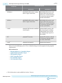
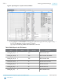
Table 1: Peripherals that Support Signal Routing from the HPS Domain to FPGA Domain
The following table lists the interface type that is available depending on whether the IP interface is pinned out in
the HPS domain or the FPGA domain.
Interface Description
Peripherals
HPS Domain
FPGA Domain
EMAC
RGMII Interface
GMII Interface
QSPI
Standard QSPI interface with four
slave select signals
Standard QSPI interface with
four slave select signals achieved
by connecting exported signals
to bidirectional buffers
© 2015 Altera Corporation. All rights reserved. ALTERA, ARRIA, CYCLONE, ENPIRION, MAX, MEGACORE, NIOS, QUARTUS and STRATIX words and logos are
trademarks of Altera Corporation and registered in the U.S. Patent and Trademark Office and in other countries. All other words and logos identified as
trademarks or service marks are the property of their respective holders as described at www.altera.com/common/legal.html. Altera warrants performance
of its semiconductor products to current specifications in accordance with Altera's standard warranty, but reserves the right to make changes to any
products and services at any time without notice. Altera assumes no responsibility or liability arising out of the application or use of any information,
product, or service described herein except as expressly agreed to in writing by Altera. Altera customers are advised to obtain the latest version of device
specifications before relying on any published information and before placing orders for products or services.
www.altera.com
101 Innovation Drive, San Jose, CA 95134
ISO
9001:2008
Registered
2
AN-706
2014.07.17
HPS Peripherals That Support Routing to the FPGA
Interface Description
Peripherals
HPS Domain
FPGA Domain
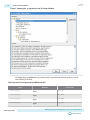
SPI Master
MOSI/MISO SPI interface configu‐
rable to single or dual slaves
MOSI/MISO SPI interface with
output enables that support up
to four slaves; interface achieved
by connecting exported signals
to bidirectional buffers
SPI Slave
MOSI/MISO SPI interface configu‐
rable to single or dual slaves
MOSI/MISO SPI interface with
output enables that support up
to four slaves; interface achieved
by connecting exported signals
to bidirectional buffers
UART
Standard UART interface with flow
control signals
Standard UART interface with
flow control signals, including
DTR and DSR; status and two
user-defined output signals are
also available
I2C
Standard I2C interface
Standard I2C interface achieved
by connecting exported signals
to a bidirectional buffer
CAN(1)
Standard CAN interface
Standard CAN interface
Please refer to the following Cyclone V Device Handbook chapters for descriptions of each peripheral
signal interface:
Related Information
•
•
•
•
•
•
(1)
Ethernet Media Access Controller Chapter
Quad SPI Flash Controller Chapter
SPI Controller Chapter
UART Controller Chapter
I2C Controller Chapter
CAN Controller Chapter
The CAN interface is only available for Cyclone V devices.
Altera Corporation
AN 706: Mapping HPS IP Peripheral Signals to the FPGA Interface
Send Feedback
AN-706
2014.07.17
HPS IP Interface to FPGA Design Example
3
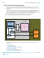
HPS IP Interface to FPGA Design Example
This design example, based on the Golden System Reference Design (GSRD), uses the Cyclone V SoC
development kit resources to demonstrate routing the HPS EMAC0 and I2C0 peripheral signals to the
FPGA interface.
The HPS component provides up to two EMAC peripherals, which support 10/100/1000 Mbps operation.
The Cyclone V SoC Development board is populated with a Micrel KSZ9021RN RGMII PHY that
interfaces to the HPS domain and a Renesas uPD60620A MII Dual Port PHY that interfaces to the FPGA
domain. The HPS and FPGA also share a common I2C bus to various on-board I2C slaves.
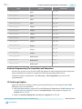
Figure 1: High-level Routing Layout of Cyclone V SoC Board Design Example
Cyclone V SoC Development Board
Altera 5CSXFC6D6F31C6
FPGA Domain
Cortex-A9 MPU
Subsystem
L3 Interconnect
AXI
Bridge
Qsys System
10/100 Ethernet
EMAC0
I2C0
GMII Signals
I2C Signals
Renesas PHY
I2C Slaves
The following sections provide the necessary information to route the HPS peripherals to the FPGA
interface, such as:
1.
2.
3.
4.
5.
6.
Prerequisites on page 4
Getting Started on page 5
Generating the Initial HDL in Qsys on page 5
Top Level Routing on page 9
Timing Constraint Configuration on page 11
Quartus II Pin Assignments on page 11
AN 706: Mapping HPS IP Peripheral Signals to the FPGA Interface
Send Feedback
Altera Corporation
4
AN-706
2014.07.17
Prerequisites
7. Hardware Programming File Compilation and Generation on page 13
8. SD Card Image Updates on page 13
9. Board Setup and Booting Linux from the SD Card on page 15
Prerequisites
This design example is based on the Cyclone V GSRD and tested with Quartus II version 14.0. Refer to the
links listed below and review the recommended material before starting with this design example.
Related Information
• Cyclone V SoC Development Kit
Refer to this link for Cyclone V SoC Development Kit documentation and installation files.
• Golden System Reference Design User's Manual
Refer to this document and step through the Getting Started Guides, Prerequisites, and the GHRD
Overview. In addition, review the Development Flow Overview.
Hardware Requirements
The hardware required for this design example is:
• Cyclone V SoC Development Kit
• RJ45 Ethernet cable
• SD/MMC card preloaded with default GSRD image
Software Requirements
The software required for this design example is:
• Quartus II 14.0 and above
• SoC EDS 14.0 and above
• Factory default hardware template cv_soc_devkit_ghrd in SoC EDS 14.0
Design example files are provided in the AN 706 design example link and are listed in the table below.
Table 2: Required Software Files
File Name
Description
ghrd_top.v
Top level RTL file
soc_system_timing.sdc
Timing constraint file
an706_de_pin_assignment.tcl
Pin assignment script file
preloader-mkpimage.bin
Generated preloader binary targeted to this project
u-boot.img
Modified u-boot image for EMAC0
socfpga.dtb
Modified device tree for EMAC0 and I2C0
Altera Corporation
AN 706: Mapping HPS IP Peripheral Signals to the FPGA Interface
Send Feedback
AN-706
2014.07.17
Getting Started
5
Getting Started
1. Make a copy of the Cyclone V Golden Hardware Reference Design (GHRD) from your Cyclone
V SoC Development Kit installation location or download the latest Cyclone V GHRD design example
from the Rocketboards website to your project location.
2. Download the AN 706 design files (an706-design-files.zip) provided.
3. Open the GHRD project within the Quartus II software.
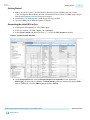
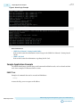
Generating the Initial HDL in Qsys
1. In the Quartus II navigation bar, select Tools > Qsys.
2. In the Qsys window, select File > Open > soc_system.qsys.
3. In the System Contents tab, double click on hps_0 to open the HPS Parameters window.
Figure 2: System Contents Window
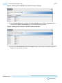
4. On the Peripheral Pins tab, under the Ethernet Media Access Controller section, click on the
EMAC0 pin pull-down and select FPGA. The EMAC0 mode pull-down automatically displays Full to
indicate GMII mode. Select the EMAC1 pin pull-down as Unused.
AN 706: Mapping HPS IP Peripheral Signals to the FPGA Interface
Send Feedback
Altera Corporation
6
AN-706
2014.07.17
Generating the Initial HDL in Qsys
Figure 3: Selecting FPGA for EMAC0 Pin in the HPS Parameters Window
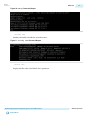
5. On the Peripheral Pins tab, scroll down to the I2C Controllers section, click on the I2C0 pin pulldown and select FPGA. The I2C0 mode pull-down automatically displays Full.
Figure 4: Selecting FPGA for I2C0 Pin in the HPS Parameters Window
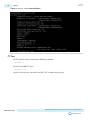
6. Return to the System Contents tab and in the Export column, double-click on the EMAC0 and I2C0
signal pins to export them as conduits.
Altera Corporation
AN 706: Mapping HPS IP Peripheral Signals to the FPGA Interface
Send Feedback
AN-706
2014.07.17
Generating the Initial HDL in Qsys
7
Figure 5: Exporting Pins in System Contents Window
7. Select Generate > Generate HDL from the Qsys menu bar. In the project directory, replace the top
level RTL file, ghrd_top.v, with the generated Verilog file.
Qsys exposes the following EMAC0 and I2C0 interfaces in the file:
Table 3: EMAC0 Signals in the FPGA Domain
Signal
emac0_phy_txd_o
Width
Direction
Description
8
Out
PHY Transmit Data
emac0_phy_txen_o 1
Out
PHY Transmit Data Enable
emac0_phy_txer_o
1
Out
PHY Transmit Error
emac0_phy_rxdv_i
1
In
PHY Receive Data Valid
emac0_phy_rxer_i
1
In
PHY Receive Error
emac0_phy_rxd_i
8
In
PHY Receive Data
emac0_phy_col_i
1
In
PHY Collision Detect
AN 706: Mapping HPS IP Peripheral Signals to the FPGA Interface
Send Feedback
Altera Corporation
8
AN-706
2014.07.17
Generating the Initial HDL in Qsys
Signal
Width
Direction
Description
emac0_phy_crs_i
1
In
PHY Carrier Sense
emac0_gmii_mdo_
o
1
Out
MDIO signal data out
emac0_gmii_mdo_
o_e
1
Out
MDIO signal output enable
emac0_gmii_mdi_i
1
In
MDIO signal input
emac0_gmii_mdc_o 1
Out
Management Data Clock
emac0_clk_rx_i
1
In
PHY RX reference clock
emac0_clk_tx_i
1
In
PHY TX reference clock
emac0_phy_txclk_o 1
Out
Transmit clock output to the
PHY
emac0_rst_clk_tx_
n_o
1
Out
Transmit clock reset output to
the FPGA interface
emac0_rst_clk_rx_
n_o
1
Out
Receive clock reset output
Table 4: I2C0 Signals in the FPGA Domain
Signal
Width
Direction
Description
i2c0_out_data
1
Out
Outgoing I2C data
enable
i2c0_sda
1
In
Incoming I2C data
i2c0_clk_clk
1
Out
Outgoing I2C clock
enable
i2c0_scl_in_clk
1
In
Incoming I2C clock
source
Related Information
• Ethernet Media Access Controller
Refer to the interface descriptions in the Ethernet Media Access Controller chapter of the HPS
Technical Reference Manual for more detailed GMII interface signal descriptions
Altera Corporation
AN 706: Mapping HPS IP Peripheral Signals to the FPGA Interface
Send Feedback
AN-706
2014.07.17
Top Level Routing
9
• I2C Controller
Refer to the interface descriptions in the I2C Controller chapter of the HPS Technical Reference Manual
for more detailed I2C interface signal descriptions.
Top Level Routing
The top level RTL file defines the pin connections from the HPS EMAC0 to the Renesas MII PHY on the
Cyclone V SoC development board.
Note: Because MII is a 4-bit data width protocol, connect only the lower 4-bits, emac0_phy_txd_o[3:0]
and emac0_phy_rxd_i[3:0], of EMAC0's RX and TX interface from the FPGA.
AN 706: Mapping HPS IP Peripheral Signals to the FPGA Interface
Send Feedback
Altera Corporation
10
AN-706
2014.07.17
Top Level Routing
Figure 6: Routing of the EMAC0 FPGA Interface to the On-board MII PHY
HPS-to-FPGA Signal Interface
PHY Signal Interface
gmii_mdo_o_e
MDIO
gmii_mdo_o
gmii_mdi_i
MDC
gmii_mdc_o
phy_txd_o[3]
P0_TXD[3]
phy_txd_o[2]
P0_TXD[2]
phy_txd_o[1]
P0_TXD[1]
phy_txd_o[0]
P0_TXD[0]
phy_txen_o
P0_TXEN
phy_txer_o
P0_TXER
phy_rxd_i[3]
P0_RXD[3]
phy_rxd_i[2]
P0_RXD[2]
phy_rxd_i[1]
P0_RXD[1]
phy_rxd_i[0]
P0_RXD[0]
phy_rxdv_i
P0_RXDV
phy_rxer_i
P0_RXER
clk_rx_i
P0_RXCLK
clk_tx_i
P0_TXCLK
phy_txclk_o / gtx_clk
rst_clk_tx_n_o
rst_clk_rx_n_o
phy_col_i
P0_CRS
phy_crs_i
P0_COL
HPS I2C0 is routed through the FPGA interface and acts as a master to various on-board I2C slaves:
•
•
•
•
Two Octal Digital Power Supply Managers with EEPROM
LCD
RTC
EEPROM
Note: A bi-directional buffer, alt_iobuff, must be added in the design to connect the I2C signals to an
external open drain IO. The buffer can be included by instantiating alt_iobuff in ghrd_top.v.
Altera Corporation
AN 706: Mapping HPS IP Peripheral Signals to the FPGA Interface
Send Feedback
AN-706
2014.07.17
Timing Constraint Configuration
11
The following Verilog code shows the alt_iobuff instantiation for an I2C interface implemented
through the FPGA:
ALT_IOBUF scl_iobuf (.i(1'b0),
declared bi-directional buffer
ALT_IOBUF sda_iobuf (.i(1'b0),
declared bi-directional buffer
.oe(scl_o_e), .o(scl_o), .io(fpga_i2c_scl)); //
for scl
.oe(sda_o_e), .o(sda_o), .io(fpga_i2c_sda)); //
for sda
Related Information
alt_iobuff Primitive
Refer to the alt_iobuff primitive information for more information.
Timing Constraint Configuration
Replace the soc_system_timing.sdc file in your project directory with the soc_system_timing.sdc file provided
in the project folder. This new file is customized for the EMAC0 and I2C0 interface being tested on the
Cyclone V SoC development board.
Quartus II Pin Assignments
1. Copy an706_de_pin_assignment.tcl from the AN 706 design files into your project directory.
2. In the Quartus II menu bar, select Tools > Tcl Scripts
3. In the Tcl Scripts window, choose an706_de_pin_assignment.tcl and select Run.
AN 706: Mapping HPS IP Peripheral Signals to the FPGA Interface
Send Feedback
Altera Corporation
12
AN-706
2014.07.17
Quartus II Pin Assignments
Figure 7: Selecting pin_assigment.tcl in the Tcl Scripts Window
The an706_de_pin_assignment.tcl script automatically assigns EMAC0 and I2C0 signal pins to their
related FPGA pin location.
Table 5: Quartus Pin Assignments for EMAC0 and I2C0
Signal
Direction
Pin Location
enet1_rx_clk
Input
PIN_Y24
enet1_rx_d[0]
Input
PIN_AB23
enet1_rx_d[1]
Input
PIN_AA24
enet1_rx_d[2]
Input
PIN_AB25
Altera Corporation
AN 706: Mapping HPS IP Peripheral Signals to the FPGA Interface
Send Feedback
AN-706
2014.07.17
Hardware Programming File Compilation and Generation
Signal
Direction
13
Pin Location
enet1_rx_d[3]
Input
PIN_AE27
enet1_rx_dv
Input
PIN_Y23
enet1_rx_error
Input
PIN_AE28
enet1_tx_clk_fb
Input
PIN_W25
enet1_tx_d[0]
Output
PIN_W20
enet1_tx_d[1]
Output
PIN_Y21
enet1_tx_d[2]
Output
PIN_AA25
enet1_tx_d[3]
Output
PIN_AB26
enet1_tx_en
Output
PIN_AB22
enet1_tx_error
Output
PIN_AG5
enet_dual_resetn
Output
PIN_AJ1
enet_fpga_mdc
Output
PIN_H12
enet_fpga_mdio
Bidirectional
PIN_H13
fpga_i2c_scl
Bidirectional
PIN_G7
fpga_i2c_sda
Bidirectional
PIN_F6
Hardware Programming File Compilation and Generation
After the Qsys system is set up, the top level RTL file updated, the related signal pin location assigned and
timing constrained, the design can be compiled and the SOF programming file generated.
In Quartus II software navigation bar, select Processing > Start Compilation to generate the SOF
programming file.
SD Card Image Updates
Update the default SD card image with the generated preloader binary, u-boot image file and DTB file
following the steps described below:
1. With your Linux machine, prepare the SD card by following the information in GSRD-Booting Linux
Using Prebuilt SD Card Image. Untar the sd_image.bin.tar.gz file and program the image file, sd_
image.bin into the SD card.
2. Replace the preloader-mkpimage.bin, u-boot.img and socfpga.dtb in the SD card.
AN 706: Mapping HPS IP Peripheral Signals to the FPGA Interface
Send Feedback
Altera Corporation
14
AN-706
2014.07.17
Preloader Generation
Note: Information provided regarding SD card changes, preloader and Linux software file changes
and preloader generation are applicable to this reference design only.
Preloader Generation
Because this design example modifies the default GHRD Qsys file, it is essential to re-generate the
preloader with the preloader generator.
Related Information
GSRD - Generating and Compiling the Preloader
Refer to this location for information on how to generate and compile the preloader.
U-boot Setup
Go to file location u-boot-socfpga/include/configs/socfpga_cyclone.h. The EMAC0 parameters associated
with the interface speed must be configured to MII in the socfpga_cyclone.h file in the u-boot source.
Change the #define for CONFIG_EMAC_BASE and CONFIG_PHY_INTERFACE_MODE to the following:
#define CONFIG_EMAC_BASE
#define CONFIG_PHY_INTERFACE_MODE
CONFIG_EMAC0_BASE
SOCFPGA_PHYSEL_ENUM_MII
Related Information
Preloader and U-Boot Customization
Refer to this location for information on how to customize u-boot.
Device Tree Setup
Generate the device tree. EMAC0 is enabled in the device tree source, as shown below, and the I2C0 code
source maintains its default settings.
aliases
{
ethernet0 = "/soc/ethernet@ff700000";
};
ethernet@ff700000 {
compatible = "altr,socfpga-stmmac","snps,dwmac-3.70a",
"snps,dwmac";
reg = <0xff700000 0x2000>;
interrupts = <0x0 0x73 0x4>;
interrupt-names = "macirq";
mac-address = [00 00 00 00 00 00];
clocks = <0xd>;
clock-names = "stmmaceth";
status = "okay";
phy-mode = "mii";
phy-add r= <0xffffffff>;
snsp,
};
Related Information
GSRD User Manual - Device Tree Generator
Refer to this location for information on device tree generation.
Altera Corporation
AN 706: Mapping HPS IP Peripheral Signals to the FPGA Interface
Send Feedback
AN-706
2014.07.17
Board Setup and Booting Linux from the SD Card
15
Board Setup and Booting Linux from the SD Card
Before you begin
Board setup is based on the GSRD Getting Started Guides.
1. Connect Ethernet Cable to the ENET1 Ethernet port.
Figure 8: Ethernet Connection on Cyclone V SoC Development Board
2. Slot in the SD card and power on the board.
3. Program the FPGA .sof file and perform a warm reset on the HPS component to reload the SD card
image.
4. The kernel automatically enables and initializes EMAC0 then executes the dynamic host configuration
protocol (DHCP) to obtain an IP address.
5. When the boot process has completed, login as root at the kernel terminal.
AN 706: Mapping HPS IP Peripheral Signals to the FPGA Interface
Send Feedback
Altera Corporation
16
AN-706
2014.07.17
Sample Application Example
Figure 9: Kernel Login Example
Related Information
• GSRD User's Manual - Getting Started Guides
Refer to this location for information on board setup in the GSRD User's Manual - Getting Started
Guides.
• GSRD - SD Card
Refer to this location for information on updating the SD Card.
Sample Application Example
The default kernel image contains many useful commands and built-in tools, such as ethtools and miitools. Some examples are illustrated in this section.
EMAC Test
Examples of commands that can be executed on EMAC0 are:
>udhcpc
Activate the dhcp server to request an IP address.
Altera Corporation
AN 706: Mapping HPS IP Peripheral Signals to the FPGA Interface
Send Feedback
AN-706
2014.07.17
EMAC Test
17
Figure 10: udhcpc Command Output
>ifconfig eth0
Initialize and enable or disable the network interface.
Figure 11: ifconfig eth0 Command Output
>ethtool eth0
Display and allow edits to the EMAC device parameters.
AN 706: Mapping HPS IP Peripheral Signals to the FPGA Interface
Send Feedback
Altera Corporation
18
AN-706
2014.07.17
I2C Test
Figure 12: ethtool eth0 Command Output
I2C Test
The I2C interface can be tested using the following commands:
>i2cdetect -l
List the detected HPS I2C ports.
>i2cdetect -r 0
List the I2C slave devices connected to the HPS. "UU" is defined as device busy.
Altera Corporation
AN 706: Mapping HPS IP Peripheral Signals to the FPGA Interface
Send Feedback
AN-706
2014.07.17
I2C Test
19
Figure 13: i2cdetect Command Outputs
>i2cset -y 0 0x66 0x10 0x55
I2C0 writes the data value 0x55 to the data address 0x10 of slave device at 0x66. The command is written
in the order: device address, data address, data value.
>i2cget -y 0 0x66 0x10
Return data value at address 0x10 of the device slave at address 0x66.
Figure 14: i2cset and i2cget Commands
>i2cdump -y 0 0x66
Register data dump from 0x00 to 0xFF. "XX" is defined as a non-valid address.
AN 706: Mapping HPS IP Peripheral Signals to the FPGA Interface
Send Feedback
Altera Corporation
20
AN-706
2014.07.17
Reference Documents
Figure 15: i2cdump Command Output
Reference Documents
A summary list of the reference documents and sites mentioned in this application note follows:
Related Information
•
•
•
•
•
•
•
•
•
•
•
•
•
•
Altera Corporation
HPS-to-FPGA Application Note (AN 706) Design Example
Cyclone V SoC Development Kit
Golden System Reference Design User's Manual
Compiling Golden Hardware Reference Design
Ethernet Media Access Controller
I2C Controller
alt_iobuff Primitive
GSRD-Booting Linux Using Prebuilt SD Card Image
GSRD - Generating and Compiling the Preloader
Preloader and U-Boot Customization
GSRD User Manual - Device Tree Generator
GSRD User's Manual - Getting Started Guides
GSRD - SD Card
RocketBoard website
AN 706: Mapping HPS IP Peripheral Signals to the FPGA Interface
Send Feedback
AN-706
2014.07.17
Revision History
21
Revision History
Date
Version
Changes
July 2014
2014.07.17
• Modified URLs of RocketBoards pages to versioned links.
• Correctd AN 706 design example URL.
• Added steps to the Board Setup and Booting Linux from the SD Card
section.
July 2014
2014.07.03
Initial Release
AN 706: Mapping HPS IP Peripheral Signals to the FPGA Interface
Send Feedback
Altera Corporation