1
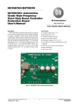
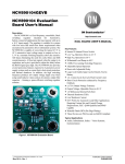
NCV887701BSTGEVB
NCV887701 Automotive
Grade High-Frequency
Start-Stop Boost Controller
Evaluation Board
User'sManual
http://onsemi.com
EVAL BOARD USER’S MANUAL
Description
Key Features
•
•
•
•
•
•
•
This NCV887701 evaluation board provides a convenient
way to evaluate a high frequency boost controller designed
to supply a minimum output voltage during Start-Stop
vehicle battery voltage sags. The unit is in low Iq sleep-mode
under normal battery operating condition and wakes-up
when the monitored voltage drops below 7.3 V and begin
regulating once 6.8 V is reached. Switching frequency is set
to 440 kHz with a user selectable ROSC resistor. The
evaluation board is rated 6.8 V / 3.6 A at a 2.6 V input
voltage. Operation below 2.6 V is possible if output current
is reduced.
•
•
Automatic Enable below 7.3 V
Disable Override Function
Boost Operation at 6.8 V
440 kHz Switching Frequency
Input Undervoltage Lockout
Wide Input Voltage of 2.6 V to 45 V
Low Quiescent Current in Sleep Mode (< 12 mA
Typical)
Cycle-by-Cycle Current Limit Protection
Automotive Grade
Figure 1. NCV887701 Start−Stop Evaluation Board
© Semiconductor Components Industries, LLC, 2014
February, 2014 − Rev. 0
1
Publication Order Number:
EVBUM2224/D
NCV887701BSTGEVB
Table 1. EVALUATION BOARD TERMINALS
Terminal
Function
VIN (large post)
Positive DC input voltage (power)
GND (large post)
Common DC return (power)
VOUT (large post)
Regulated DC output voltage (power)
GND (small post)
Common DC return, monitoring point
VC (small post)
Voltage compensation, monitoring point
VOUT (small post)
Regulated DC output voltage, monitoring point
VDRV (small post)
Driving voltage, monitoring point
DISB (small post)
Disable override input, monitoring point
ISNS (small post)
Current sense resistor voltage, monitoring point
VG (small post)
MOSFET gate voltage, monitoring point
SW (small post)
MOSFET drain voltage, monitoring point
Table 2. ABSOLUTE MAXIMUM RATINGS (Voltages are with respect to GND)
Rating
Value
Unit
DC supply voltage (VIN)
-0.3 to 45
V
DC supply voltage (EN, SYNC)
-0.3 to 6
V
DC Voltage (DISB)
-0.3 to 6
V
Junction Temperature
-40 to 150
°C
Ambient temperature (Evaluation Board)
-40 to 105
°C
Stresses exceeding those listed in the Maximum Ratings table may damage the device. If any of these limits are exceeded, device functionality
should not be assumed, damage may occur and reliability may be affected.
Table 3. ELECTRICAL CHARACTERISTICS
(TA = 25°C, 2.6 V ≤ VIN ≤ Vout_LED, VDISB = 5 V, unless otherwise specified)
Conditions
Typical Value
Unit
ROSC = 10.7 kW
440
kHz
ROSC (refer to datasheet)
170-500
kHz
-
18
A
-
0.83
-
VOUT Undervoltage Lockout (UVLO)
VOUT falling
3.8
V
Thermal Shutdown
TA increasing
170
°C
Characteristics
Switching
Switching Frequency
User Selectable Frequency Range
Current Limit
Cycle-by-cycle Current Limit (FET)
Protections
Maximum Duty Cycle
Product parametric performance is indicated in the Electrical Characteristics for the listed test conditions, unless otherwise noted. Product
performance may not be indicated by the Electrical Characteristics if operated under different conditions.
http://onsemi.com
2
NCV887701BSTGEVB
Operational Guidelines
3. Connect a 3.6 A constant current load on the
output.
4. Decrease the DC input voltage until the PCB VIN
voltage is 5.5 V ±0.5 V.
5. Set the DISB control signal to a TTL high state
(i.e. 5 V).
6. Verify that the unit is regulating at VOUT = 6.8 V.
7. Reduce the DC input voltage until the PCB
VIN = 2.6 V. Verify that the unit is regulating at
VOUT = 6.8 V.
The evaluation board is rated to operate under full load for
input voltage as low as 2.6 V at the input terminal under full
power (less if output current is reduced). Start-Stop
applications use reverse battery protection diodes in front of
the boost converter (Figure 2), so the input source can
operate down to 2.6 V plus a diode drop (i.e ∼3 V).
Notes:
1. The IC UVLO (undervoltage lockout) is 4.25 V
for VOUT rising, 3.8 V for VOUT falling (0.45 V
hysteresis).
2. Limit time spent with the power supply operating
at minimum input voltage (equivalent to
VIN = 2.6 V) to avoid overheating the power
semiconductors.
Start-Stop Voltage Transient Test:
1. Connect both DC1 and DC2 input power supplies
as illustrated in Figure 2. Adjust DC2 so that PCB
VIN = 2.6 V for a 3.6 A load.
2. Connect a 3.6 A load on the output. If a load
resistor is used, it is recommended to start from a
DC1 input voltage of 8.5 − 9.0 V to avoid
overstressing the PCB boost diode (D1, rated 4 A).
3. Monitor VOUT. Disconnect supply DC1. VOUT
should have a response similar to that of Figure 3.
First Time Power-Up:
1. Connect a DC source voltage (15 A capable) set to
a voltage of 12 − 13 V as shown in Figure 1.
2. Connect the DISB TTL control signal as shown in
Figure 1. The initial DISB state should be set to
logic −‘0’.
DISB Command
(TTL)
VOUT
GND
Reverse Polarity
Protection Diode Harness
PS2
(30 W capable)
DISB
VIN
3.6 A
Constant
Current
Load
NCV887701
6.8 V / 3.6 A
Evaluation Board
PS1
(15 A capable)
GND
GND
Figure 2. Evaluation Board Connections
http://onsemi.com
3
NCV887701BSTGEVB
Typical Performance
DC1 is disabled, then re-enabled
Figure 3. NCV887701 Evaluation Board Waveforms
− DC2 at VIN adjusted to 2.6 V (after reverse polarity protection diode)
− VOUT = 6.8 V, IOUT = 3.6 A
http://onsemi.com
4
NCV887701BSTGEVB
SCHEMATIC
Figure 4. NCV887701 Boost 6.8 V / 3.6 A Evaluation Board Schematic
http://onsemi.com
5
NCV887701BSTGEVB
BILL OF MATERIALS
Table 4. BILL OF MATERIALS*
Manufacturer’s Part
Number
Substitution
Allowed
Murata Electronics
North America
GCM1885C1H471JA16D
Yes
10%
TDK Corporation
CGA3E2X7R1H333K080AA
Yes
1 mF
10%
Murata Electronics
North America
GCM188R71C105KA64D
Yes
CAP CER 1UF 50V 10%
X7R 0805
1.0 mF
10%
TDK Corporation
CGA4J3X7R1H105K125AB
Yes
1
CAP CER 150PF 50V
5% NP0 0603
150 pF
5%
Murata Electronics
North America
GCM1885C1H151JA16D
Yes
CI1, CO6
2
CAP CER 0.1UF 50V
10% X7R 0805
100 nF
10%
Murata Electronics
North America
GCM21BR71H104KA37L
Yes
CI2
1
CAP ALUM 220UF 50V
20% SMD
220 mF
20%
Chemi−Con
EMZA500ADA221MJA0G
Yes
CI3
1
CAP ALUM 470UF 50V
20% RADIAL
470 mF
20%
Panasonic Electronic
Components
EEU-FC1H471
Yes
CO2, CO3,
CO4
3
CAP ALUM 100UF 35V
20% SMD
100 mF
20%
Nichicon
RHS1V101MCN1GS
No
CO5
1
CAP CER 4.7UF 50V
10% X7R 1210
4.7 mF
10%
Murata Electronics
North America
GCM32ER71H475KA55L
Yes
CSNB
1
CAP CER 3300PF 50V
5% NP0 0603
3300 pF
5%
TDK Corporation
CGA3E2C0G1H332J080AA
Yes
D1
1
40 V, 4.0 A Schottky
Rectifier SO8-FL
40 V /
4A
N/A
ON Semiconductor
NRVB440MFST1G
No
L1
1
INDUCTOR POWER
2.2UH 22A SMD
2.2 mH
20%
Vishay Dale
IHLP5050FDER2R2M01
No
Q1
1
N-Channel Power
MOSFET 60V 61A
SO-8FL
60 V /
61 A
N/A
ON Semiconductor
NVMFS5844NL
No
R1
1
RES 3.01K OHM 1/10W
1% 0603 SMD
3.01 KW
1%
Vishay Dale
CRCW06033K01FKEA
Yes
R2
1
RES 10.7K OHM 1/10W
1% 0603 SMD
10.7 KW
1%
Vishay Dale
CRCW060310K7FKEA
Yes
R3
1
RES 0.0 OHM 1/10W
JUMP 0603 SMD
0
Jumper
Vishay Dale
CRCW06030000Z0EA
Yes
R4
1
RES 249 OHM 1/10W
1% 0603 SMD
249 W
1%
Vishay Dale
CRCW0603249RFKEA
Yes
R6
DNP
R7, R8
2
RES 0.022 OHM 1W 5%
1206 SMD
0.022 W
5%
Panasonic Electronic
Components
ERJ-8BWJR022V
No
RDAMP
1
RES 0.68 OHM 1/10W
1% 0603 SMD
0.68 W
1%
Panasonic Electronic
Components
ERJ-3RQFR68V
Yes
RSNB
1
RES 5.6 OHM 1/10W
1% 0603 SMD
5.6 W
1%
Vishay Dale
CRCW06035R60FKEA
Yes
U1
1
Automotive Non-Sync
Boost Controller
N/A
N/A
ON Semiconductor
NCV887701
No
Reference
Designator(s)
QTY
Description
Value
Tolerance
C1
1
CAP CER 470PF 50V
5% NP0 0603
470 pF
5%
C2
1
CAP CER 0.033UF 50V
10% X7R 0603
0.033 mF
C3
1
CAP CER 1UF 16V 10%
X7R 0603
C4, CO1
2
C5
Manufacturer
*All Materials are RoHS Compliant
http://onsemi.com
6
NCV887701BSTGEVB
PCB LAYOUT
Figure 5. Top View
Figure 6. Bottom View
http://onsemi.com
7
NCV887701BSTGEVB
ON Semiconductor and
are registered trademarks of Semiconductor Components Industries, LLC (SCILLC). SCILLC owns the rights to a number of patents, trademarks,
copyrights, trade secrets, and other intellectual property. A listing of SCILLC’s product/patent coverage may be accessed at www.onsemi.com/site/pdf/Patent−Marking.pdf. SCILLC
reserves the right to make changes without further notice to any products herein. SCILLC makes no warranty, representation or guarantee regarding the suitability of its products for any
particular purpose, nor does SCILLC assume any liability arising out of the application or use of any product or circuit, and specifically disclaims any and all liability, including without
limitation special, consequential or incidental damages. “Typical” parameters which may be provided in SCILLC data sheets and/or specifications can and do vary in different applications
and actual performance may vary over time. All operating parameters, including “Typicals” must be validated for each customer application by customer’s technical experts. SCILLC
does not convey any license under its patent rights nor the rights of others. SCILLC products are not designed, intended, or authorized for use as components in systems intended for
surgical implant into the body, or other applications intended to support or sustain life, or for any other application in which the failure of the SCILLC product could create a situation where
personal injury or death may occur. Should Buyer purchase or use SCILLC products for any such unintended or unauthorized application, Buyer shall indemnify and hold SCILLC and
its officers, employees, subsidiaries, affiliates, and distributors harmless against all claims, costs, damages, and expenses, and reasonable attorney fees arising out of, directly or indirectly,
any claim of personal injury or death associated with such unintended or unauthorized use, even if such claim alleges that SCILLC was negligent regarding the design or manufacture
of the part. SCILLC is an Equal Opportunity/Affirmative Action Employer. This literature is subject to all applicable copyright laws and is not for resale in any manner.
PUBLICATION ORDERING INFORMATION
LITERATURE FULFILLMENT:
Literature Distribution Center for ON Semiconductor
P.O. Box 5163, Denver, Colorado 80217 USA
Phone: 303−675−2175 or 800−344−3860 Toll Free USA/Canada
Fax: 303−675−2176 or 800−344−3867 Toll Free USA/Canada
Email: [email protected]
N. American Technical Support: 800−282−9855 Toll Free
USA/Canada
Europe, Middle East and Africa Technical Support:
Phone: 421 33 790 2910
Japan Customer Focus Center
Phone: 81−3−5817−1050
http://onsemi.com
8
ON Semiconductor Website: www.onsemi.com
Order Literature: http://www.onsemi.com/orderlit
For additional information, please contact your local
Sales Representative
EVBUM2224/D