1
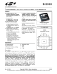
Si5338 I 2 C - P ROGR AMMABLE A NY - R ATE , A N Y -O UTPUT Q UAD C LOCK G E N E R A T O R Features Gigabit Ethernet PCI Express 2.0 OC-3/12, SFI-5 Processor, memory clocking Broadcast video xDSL PON T1/E1 SDA VDDO0 CLK0B CLK1A IN2 CLK1B VDDO1 IN3 GND GND IN4 VDDO2 IN5 CLK2A IN6 CLK2B SCL IN1 VDDO3 Applications Top View CLK3A I2C/SMBus compatible interface Easy to use programming software Small size: 4 x 4 mm, 24-QFN Low power: 45 mA core supply typ Wide temperature range: –40 to +85 °C RSVD_GND Pin Assignments CLK0A Ordering Information: See page 32. CLK3B VDD Independent core supply voltage: 1.8, 2.5, 3.3 V Independent Frequency increment/ decrement feature enables glitchless frequency adjustments in 1 ppm steps Independent phase adjustment on each of the output drivers with an accuracy of <20 ps steps Highly configurable spread spectrum on any output: Any frequency from 5 to 350 MHz Any spread from 0.5 to 5.0% Any modulation rate from 33 to 63 kHz External feedback mode allows zero-delay buffer implementation Loss of lock and loss of signal alarms VDD Low power MultiSynth technology enables independent, any-rate frequency synthesis on four differential output drivers Highly-configurable output drivers support up to four differential outputs or eight single-ended clock outputs or a combination of both Low phase jitter of 0.7 ps RMS typ High precision synthesis allows true zero ppm frequency accuracy on all outputs Flexible input reference: External crystal: 8 to 30 MHz CMOS input: 5 to 200 MHz SSTL/HSTL input: 5 to 350 MHz Differential input: 5 to 710 MHz Independently configurable outputs support any frequency or format: LVPECL/LVDS: 0.16 to 710 MHz HCSL: 0.16 to 250 MHz CMOS: 0.16 to 200 MHz SSTL/HSTL: 0.16 to 350 MHz Independent output voltage per driver: 1.5, 1.8, 2.5, or 3.3 V INTR Description The Si5338 is a high performance, low jitter clock generator capable of synthesizing any frequency on each of the device's four output drivers. The device is capable of operating in asynchronous mode for replacing free-running crystal oscillators (XO), or in a synchronous mode for translating any frequency to any other frequency within its supported frequency range. Using its patented MultiSynth technology, the Si5338 allows generation of four independent clocks with 0 ppm precision. Each output clock is independently configurable to support any of the supported signal format and supply voltages. The Si5338 provides low jitter frequency synthesis with outstanding frequency flexibility in a space-saving 4 x 4 mm QFN package. The device is programmable via an I2C/SMBuscompatible serial interface and supports operation from a 1.8, 2.5, or 3.3 V core supply. Rev. 0.5 10/09 Copyright © 2009 by Silicon Laboratories Si5338 Si5338 Functional Block Diagram Output Selectors Osc IN1 IN2 IN3 IN4 IN5 IN6 VDDO0 Input Selector CLKIN CLKINB FDBK FDBK MultiSynth ÷M0 ÷R0 fb ÷P2 Phase Frequency Detector Loop Filter VCO MultiSynth ÷M1 ÷R1 VDDO1 VDDO2 MultiSynth ÷M2 ÷R2 CLK2A CLK2B VDDO3 OEB/PINC/FINC MultiSynth ÷M3 I2C_LSB/PDEC/FDEC 2 CLK1A CLK1B FDBKB MultiSynth ÷N SCL SDA INTR CLK0A CLK0B ref ÷P1 CLKIN Analog Phase-Locked Loop Control NVM (OTP) RAM Rev. 0.5 ÷R3 CLK3A CLK3B Si5338 TABLE O F C ONTENTS Section Page 1. Electrical Specifications . . . . . . . . . . . . . . . . . . . . . . . . . . . . . . . . . . . . . . . . . . . . . . . . . . .4 2. Typical Application Circuits . . . . . . . . . . . . . . . . . . . . . . . . . . . . . . . . . . . . . . . . . . . . . . . 15 3. Functional Description . . . . . . . . . . . . . . . . . . . . . . . . . . . . . . . . . . . . . . . . . . . . . . . . . . . 16 3.1. Overview . . . . . . . . . . . . . . . . . . . . . . . . . . . . . . . . . . . . . . . . . . . . . . . . . . . . . . . . . . 16 3.2. Input Stage . . . . . . . . . . . . . . . . . . . . . . . . . . . . . . . . . . . . . . . . . . . . . . . . . . . . . . . . 17 3.3. Synthesis Stages . . . . . . . . . . . . . . . . . . . . . . . . . . . . . . . . . . . . . . . . . . . . . . . . . . . 17 3.4. Output Stage . . . . . . . . . . . . . . . . . . . . . . . . . . . . . . . . . . . . . . . . . . . . . . . . . . . . . . .18 3.5. Configuring the Si5338 . . . . . . . . . . . . . . . . . . . . . . . . . . . . . . . . . . . . . . . . . . . . . . . 18 3.6. Status Indicators . . . . . . . . . . . . . . . . . . . . . . . . . . . . . . . . . . . . . . . . . . . . . . . . . . . . 19 3.7. Output Enable . . . . . . . . . . . . . . . . . . . . . . . . . . . . . . . . . . . . . . . . . . . . . . . . . . . . . . 20 3.8. Useful Features of the Si5338 . . . . . . . . . . . . . . . . . . . . . . . . . . . . . . . . . . . . . . . . . .20 4. Applications of the Si5338 . . . . . . . . . . . . . . . . . . . . . . . . . . . . . . . . . . . . . . . . . . . . . . . . .21 4.1. Free-Running Clock Generator . . . . . . . . . . . . . . . . . . . . . . . . . . . . . . . . . . . . . . . . . 21 4.2. Synchronous Frequency Translation . . . . . . . . . . . . . . . . . . . . . . . . . . . . . . . . . . . . 21 4.3. Configurable Buffer and Level Translator . . . . . . . . . . . . . . . . . . . . . . . . . . . . . . . . . 22 5. I2C Interface . . . . . . . . . . . . . . . . . . . . . . . . . . . . . . . . . . . . . . . . . . . . . . . . . . . . . . . . . . . . 23 6. Pin Descriptions . . . . . . . . . . . . . . . . . . . . . . . . . . . . . . . . . . . . . . . . . . . . . . . . . . . . . . . . . 24 7. Device Pinout by Part Number . . . . . . . . . . . . . . . . . . . . . . . . . . . . . . . . . . . . . . . . . . . . .29 8. Package Outline: 24-Lead QFN . . . . . . . . . . . . . . . . . . . . . . . . . . . . . . . . . . . . . . . . . . . . . 30 9. Recommended PCB Layout . . . . . . . . . . . . . . . . . . . . . . . . . . . . . . . . . . . . . . . . . . . . . . . 31 10. Ordering Information . . . . . . . . . . . . . . . . . . . . . . . . . . . . . . . . . . . . . . . . . . . . . . . . . . . . 32 Document Change List . . . . . . . . . . . . . . . . . . . . . . . . . . . . . . . . . . . . . . . . . . . . . . . . . . . . .33 Contact Information . . . . . . . . . . . . . . . . . . . . . . . . . . . . . . . . . . . . . . . . . . . . . . . . . . . . . . . .34 Rev. 0.5 3 Si5338 1. Electrical Specifications Table 1. Recommended Operating Conditions (VDD = 1.8 V –5% to +10%, 2.5 V ±10%, or 3.3 V ±10%, TA = –40 to 85°C) Parameter Symbol Ambient Temperature Test Condition TA VDD Core Supply Voltage Output Buffer Supply Voltage Min Typ Max Unit –40 25 85 °C 2.97 3.3 3.63 V 2.25 2.5 2.75 V 1.71 1.8 1.98 V 1.4 — 3.63 V VDDOn Note: All minimum and maximum specifications are guaranteed and apply across the recommended operating conditions. Typical values apply at nominal supply voltages and an operating temperature of 25 °C unless otherwise noted. Table 2. Absolute Maximum Ratings Parameter Symbol Test Condition Value Unit DC Supply Voltage VDD –0.5 to 3.8 V Storage Temperature Range TSTG –55 to 150 °C ESD Tolerance HBM (100 pF, 1.5 k) 2.5 kV ESD Tolerance CDM 550 V ESD Tolerance MM 175 V JESD78 Compliant Latch-up Tolerance Note: Permanent device damage may occur if the Absolute Maximum Ratings are exceeded. Functional operation should be restricted to the conditions as specified in the operational sections of this data sheet. Exposure to absolute maximum rating conditions for extended periods may affect device reliability. Table 3. Thermal Characteristics Parameter Symbol Test Condition Value Unit Thermal Resistance Junction to Ambient Theta JA Still Air 37 °C/W 4 Rev. 0.5 Si5338 Table 4. DC Characteristics (VDD = 1.8 V –5% to +10%, 2.5 V ±10%, or 3.3 V ±10%, TA = –40 to 85°C) Parameter Core Supply Current* Output Buffer Supply Current Symbol Test Condition Min Typ Max Unit IDD 100 MHz on all outputs, 25 MHz refclk — 45 60 mA LVPECL, 710 MHz — — 30 mA LVDS, 710 MHz — — 8 mA HCSL, 250 MHz 2 pF load capacitance — — 20 mA SSTL, 350 MHz — — 19 mA CMOS, 50 MHz 15 pF load capacitance — — 28 mA CMOS, 200 MHz 2 pF load capacitance — — 28 mA HSTL, 350 MHz — — 19 mA IDDOx *Note: Output Supply Voltage = 3.63 V. The supply current is considerably lower for lower supply voltage. Rev. 0.5 5 Si5338 Table 5. Performance Characteristics (VDD = 1.8 V –5% to +10%, 2.5 V ±10%, or 3.3 V ±10%, TA = –40 to 85°C) Parameter Symbol Test Condition Min Typ Max Unit APLL Acquisition Time tACQ — — 25 ms APLL Lock Range fLOCK 5000 — — ppm APLL Loop Bandwidth fBW — 1.6 — MHz MultiSynth Frequency Synthesis Resolution fRES 0 0 1 ppb CLKIN Loss of Signal Detect Time tLOS — 2.6 5 µs CLKIN Loss of Signal Release Time tLOSRLS 0.01 0.2 1 µs APLL Loss of Lock Detect Time tLOL — 5 10 ms Reset Time tRST — — 2 ms POR to Output Clock Valid (Pre-programmed Devices) tRDY — — 2 ms Input-to-Output Propagation Delay tPROP Buffer Mode (APLL Bypass) — 2.5 — ns Outputs at same frequency, signal format — — 100 ps –45 — +45 ns Output-Output Skew tDSKEW Programmable Initial Phase Offset POFFSET Output frequency < Fvco/8 Clock multiplication ratio off by 1000 ppm Phase Increment/Decrement Accuracy PSTEP — — 20 ps Phase Increment/Decrement Range PRANGE –45 — +45 ns Frequency range for phase increment/decrement fPRANGE — — 3501 MHz Phase Increment/Decrement Update Rate PUPDATE Pin control2,3 — — 1500 kHz fSTEP R divider not used 1 — See Note 1 ppm Frequency Increment/ Decrement Step Size Notes: 1. Keep MultiSynth output frequency between 5 MHz to Fvco/8. 2. Maximum frequency is Fvco/8. 3. Update rate via I2C is limited by the time it takes to perform a write operation. 4. Default value is.5% down spread. 5. Default value is ~31.5 kHz 6 Rev. 0.5 Si5338 Table 5. Performance Characteristics (Continued) (VDD = 1.8 V –5% to +10%, 2.5 V ±10%, or 3.3 V ±10%, TA = –40 to 85°C) Parameter Symbol Test Condition Min Typ Max Unit Frequency Increment/ Decrement Range fRANGE R divider not used 5 — 3501 MHz Frequency Increment/ Decrement Update Rate fUPDATE Pin control1,2 — — 1500 kHz Spread Spectrum PP Frequency Deviation SSDEV MultiSynth Output < ~Fvco/8 0.1 — 5.04 % Spread Spectrum Modulation Rate SSDEV MultiSynth Output < ~Fvco/8 30 — 635 kHz Notes: 1. Keep MultiSynth output frequency between 5 MHz to Fvco/8. 2. Maximum frequency is Fvco/8. 3. Update rate via I2C is limited by the time it takes to perform a write operation. 4. Default value is.5% down spread. 5. Default value is ~31.5 kHz Table 6. Input and Output Clock Characteristics (VDD = 1.8 V –5% to +10%, 2.5 V ±10%, or 3.3 V ±10%, TA = –40 to 85 °C) Parameter Symbol Test Condition Min Typ Max Units 5 — 710 MHz Input Clock (AC Coupled Differential Input Clocks on Pins IN1/2, IN5/6) Frequency fIN Differential Voltage Swing VPP 710 MHz input 0.4 — 2.4 VPP Rise/Fall Time tR/tF 20%–80% — — 1.0 ns Duty Cycle DC < 1 ns tr/tf 40 — 60 % Input Impedance RIN 10 — — k Input Capacitance CIN — 3.5 — pF CMOS 5 — 200 MHz SSTL/HSTL 5 — 350 MHz –0.1 — 3.63 Vpp 200 MHz, Tr/Tf = 1.3 ns 0.8 — 3.73 V Input Clock (DC-Coupled Single-Ended Input Clock on Pins IN3/4) Frequency fIN Input Voltage VI Input Voltage Swing (CMOS Standard) Rise/Fall Time tR/tF 20%–80% — — 4 ns Duty Cycle DC < 4 ns tr/tf 40 — 60 % Input Capacitance CIN — 2 — pF Rev. 0.5 7 Si5338 Table 6. Input and Output Clock Characteristics (Continued) (VDD = 1.8 V –5% to +10%, 2.5 V ±10%, or 3.3 V ±10%, TA = –40 to 85 °C) Parameter Symbol Test Condition Min Typ Max Units 0.16 — 350 MHz 367 — 466 MHz 550 — 710 MHz HCSL 0.16 — 250 MHz VOC common mode — VDDO – 1.4 V — V VSEPP peak-to-peak singleended swing 0.55 0.8 0.96 VPP VOC common mode 1.125 1.2 1.275 V VSEPP peak-to-peak singleended swing 0.25 0.35 0.45 VPP VOC common mode 0.8 0.875 0.95 V VSEPP peak-to-peak singleended swing 0.25 0.35 0.45 VPP VOC common mode 0.35 0.375 0.400 V VSEPP peak-to-peak singleended swing 0.575 0.725 0.85 VPP tR/tF 20%–80% — — 450 ps CKn < 350 MHz 45 — 55 % 350 MHz < CLKn < 710 MHz 40 — 60 % CMOS 0.16 — 200 MHz SSTL, HSTL 0.16 — 350 MHz Output Clocks (Differential) Frequency fOUT LVPECL Output Voltage LVDS Output Voltage (2.5/3.3 V) LVDS Output Voltage (1.8 V) HCSL Output Voltage Rise/Fall Time Duty Cycle DC LVPECL, LVDS Output Clocks (Single-Ended) Frequency fOUT CMOS 20%-80% Rise/ Fall Time tR/tF 2 pF load — 0.45 0.85 ns CMOS 20%-80% Rise/ Fall Time tR/tF 15 pF load — — 1.7 ns CMOS Output Resistance — 50 — SSTL Output Resistance — 50 — HSTL Output Resistance — 50 — VDDO–.3 — CMOS Output Voltage 8 VOH 4 mA load VOL 4 mA load Rev. 0.5 — V .3 V Si5338 Table 6. Input and Output Clock Characteristics (Continued) (VDD = 1.8 V –5% to +10%, 2.5 V ±10%, or 3.3 V ±10%, TA = –40 to 85 °C) Parameter Symbol VOH VOL VOH SSTL Output Voltage VOL VOH VOL Test Condition SSTL-3 VDDOx = 2.97 to 3.63 V SSTL-2 VDDOx = 2.25 to 2.75 V SSTL-18 VDDOx = 1.71 to 1.98 V VOH HSTL Output Voltage Duty Cycle VOL VDDO = 1.4 to 1.6 V DC Rev. 0.5 Min Typ Max Units .45xVDDO+.41 — — V — — .45xVDDO –.41 V 0.5xVDDO+.41 — — V — — 0.5xVDDO –.41 V 0.5xVDDO+.34 — — — 0.5xVDDO –.34 V 0.5xVDDO +.3 — — V — — .5xVDDO –.3 V 45 — 55 % V 9 Si5338 Table 7. Control Pins Parameter Symbol Condition Typ Max Unit Input Control Pins (IN3, IN4) Input Voltage Low VIL –0.1 0.3 V Input Voltage High VIH 0.9 3.63 V Input Capacitance CIN — 4 pF Input Resistance RIN 20 — k Output Control Pins (INTR) Output Voltage Low VOL ISINK = 3 mA 0 0.4 V Rise/Fall Time 20–80% tR/tF CL < 10 pf, pull up 1 k — 10 ns Typ Max Unit 11 MHz 13 pF Table 8. Crystal Specifications for 8 to 11 MHz Parameter Symbol Min fXTAL 8 Load Capacitance (on-chip differential) cL 11 Crystal Output Capacitance cO 6 pF Equivalent Series Resistance rESR 300 Crystal Max Drive Level Spec dL 100 Symbol Min fXTAL 11 Load Capacitance (on-chip differential) cL 11 Crystal Output Capacitance Crystal Frequency 12 µW Table 9. Crystal Specifications for 11 to 19 MHz Parameter Max Unit 19 MHz 13 pF cO 5 pF Equivalent Series Resistance rESR 200 Crystal Max Drive Level Spec dL Crystal Frequency 10 Rev. 0.5 100 Typ 12 µW Si5338 Table 10. Crystal Specifications for 19 to 26 MHz Parameter Symbol Min Max Unit fXTAL 19 26 MHz Load Capacitance (on-chip differential) cL 11 13 pF Crystal Output Capacitance cO 4 pF Equivalent Series Resistance rESR 100 Crystal Max Drive Level Spec dL 100 Symbol Min fXTAL 26 Load Capacitance (on-chip differential) cL 11 Crystal Output Capacitance Crystal Frequency Typ 12 µW Table 11. Crystal Specifications for 26 to 30 MHz Parameter Max Unit 30 MHz 13 pF cO 4 pF Equivalent Series Resistance rESR 75 Crystal Max Drive Level Spec dL Crystal Frequency Rev. 0.5 100 Typ 12 µW 11 Si5338 Table 12. Jitter Specifications1 (VDD = 1.8 V –5% to +10%, 2.5 V ±10%, or 3.3 V ±10%, TA = –40 to 85 °C) Parameter Symbol Test Condition Min Typ Max Unit GbE Random Jitter (12 kHz–20 MHz)2 JGBE CLKIN = 25 MHz All CLKn at 125 MHz3 — 0.7 1 ps RMS OC-12 Random Jitter (12 kHz–5 MHz) JOC12 — 0.7 1 ps RMS JPCIERJ1 CLKIN = 25 MHz All CLKn at 100 MHz Spread Spectrum not enabled3 — 0.6 1 ps RMS JPCIERJ2 CLKIN = 25 MHz All CLKn at 100 MHz Spread Spectrum not enabled3 — 0.7 1 ps RMS PCI Express 3.0 Period Jitter CLKIN = 25 MHz All CLKn at 100 MHz Spread Spectrum not enabled3 — 8 15 ps pk-pk PCI Express 3.0 Cycle-Cycle Jitter CLKIN = 25 MHz All CLKn at 100 MHz Spread Spectrum not enabled3 — 13 30 ps pk-pk N = 10,000 cycles4 — 10 30 ps pk-pk — 17 50 ps pk-pk — 0.7 1.5 ps RMS PCI Express 3.0 Random Jitter (1.5 MHz—50 MHz)2 PCI Express 3.0 Random Jitter (12 kHz—20 MHz)2 Period Jitter Cycle-Cycle Jitter JPER JCC CLKIN = 19.44 MHz All CLKn at 155.52 MHz3 N = 10,000 cycles Output MultiSynth operated in Integer or Fractional mode.4 Random Jitter (12 kHz–20 MHz) RJ Output and feedback MultiSynth in Integer or fractional mode4 Notes: 1. All jitter measurements apply for LVDS/HCSL/LVPECL output format with a low noise differential input clock and are made with an Agilent 90804 oscilloscope. All RJ measurements use RJ/DJ separation. 2. DJ for PCI and GBE is < 5 ps pp 3. Output MultiSynth in Integer mode. 4. Input frequency > 25 Mhz and any output frequency > 5 MHz. 5. Rj is multiplied by 14; estimate the pp jitter from Rj over 212 rising edges. 12 Rev. 0.5 Si5338 Table 12. Jitter Specifications1 (Continued) (VDD = 1.8 V –5% to +10%, 2.5 V ±10%, or 3.3 V ±10%, TA = –40 to 85 °C) Parameter Symbol Test Condition Min Typ Max Unit — 3 15 ps pk-pk — 2 10 ps pk-pk Output MultiSynth operated in fractional mode4 — 13 36 ps pk-pk Output MultiSynth operated in integer mode4 — 12 20 ps pk-pk Output MultiSynth operated in fractional Deterministic Jitter DJ mode4 Output MultiSynth operated in integer 4 mode Total Jitter (12 kHz–20 MHz) TJ = DJ+14xRJ (See Note 5) Notes: 1. All jitter measurements apply for LVDS/HCSL/LVPECL output format with a low noise differential input clock and are made with an Agilent 90804 oscilloscope. All RJ measurements use RJ/DJ separation. 2. DJ for PCI and GBE is < 5 ps pp 3. Output MultiSynth in Integer mode. 4. Input frequency > 25 Mhz and any output frequency > 5 MHz. 5. Rj is multiplied by 14; estimate the pp jitter from Rj over 212 rising edges. Rev. 0.5 13 Si5338 Table 13. I2C Specifications (SCL,SDA)2 Parameter Symbol Test Condition Standard Mode Unit Fast Mode3 Min Max Min Max LOW level input voltage: VILI2C –0.5 0.3 x VDDI2C –0.5 0.3 x VDDI2C1 V HIGH level input voltage: VIHI2C 0.7 x VDDI2C 3.63 0.7 x VDDI2C1 3.63 V Hysteresis of Schmitt trigger inputs VHYS N/A N/A 0.1 — V 0 0.4 0 0.4 V N/A N/A 0 0.2 x VDDI2C V –10 10 –10 10 µA LOW Level Output Voltage (open drain or open collector) at 3 mA Sink Current VOLI2C1 VDDI2C1 = 2.5/3.3 V VDDI2C1 = 1.8 V Input Current III2C Capacitance for Each I/O Pin CII2C VIN = –0.1 to VDDI2C — 4 — 4 pF I2C Bus Timeout — Timeout Enabled 25 35 25 35 ms Notes: 1. Only I2C pullup voltages (VDDI2C) of 1.71 to 3.63 V are supported. Must write register 27[7] = 1 if the I2C bus voltage is less than 2.5 V to maintain compatibility with the I2C bus standard. 2. Refer to NXP’s UM10204 I2C-bus specification and user manual, revision 03, for further details: www.nxp.com/acrobat_download/usermanuals/UM10204_3.pdf. 3. Compliant with Fast Mode+ pending characterization. 14 Rev. 0.5 Si5338 2. Typical Application Circuits +3.3 V SD/HD/3G-SDI Video/Audio Format Converter 0.1 uF Power Supply Decoupling Capacitors (1 per VDD or VDDOx pin) 2 3 27MHz 74.25MHz 74.25/1.001 MHz 148.5MHz 148.5/1.001MHz Single-ended or Differential Inputs for Synchronous Applications 1 27 MHz XTAL 5 11 IN3 CLK0 CLK1 IN5 Si5338C CLK2 IN6 +3.3V CLK4 CLK5 1k I C Bus 12 4 2 I C Address = 0x70 or 0x71 SDI Serializer INTR CLK6 SDA CLK7 21 x 100 74.25MHz, 74.25/1.001MHz 148.5MHz, 148.5/1.001MHz 18 17 14 13 Audio Out x x Audio Processor 9 IN3 24.576MHz / 6.144 MHz 10 SCL I2C_LSB 100 MHz 22 x GND 8 19 2 GND 1k Video Processor IN2 CLK3 1k SDI Deserializer IN1 100 6 SD/HD/3G SDI OUT SD/HD/3G SDI IN VDDOD 15 VDDOB VDD 16 VDDOC Optional XTAL for Free-run Applications 20 VDDOA 24 VDD 7 PAD PAD 23 23 Storage Area Network +3.3 V disk 0.1 uF Power Supply Decoupling Capacitors (1 per VDD or VDDOx pin) 2 3 x 5 6 IN2 IN3 CLK0 CLK1 IN5 IN6 Si5338C CLK2 CLK4 CLK5 1k I2C Address = 0x70 or 0x71 19 12 4 PCIe Switch INTR CLK6 SDA CLK7 SCL I2C_LSB 23 23 37.5/75/120/150MHz 22 21 100MHz 18 17 x 66MHz 14 13 x 106.25MHz 10 9 Network Processor x GND I2C Bus GND 8 SAS2 4/8 Port Controller Ethernet Fiber Channel disk +3.3V 1k disk IN1 CLK3 1k disk 11 VDDOD 15 VDDOB VDDOA 16 VDDOC 1 25 MHz XTAL 20 VDD 24 VDD 7 SAS2 4/8 Port Controller PAD PAD Rev. 0.5 15 Si5338 3. Functional Description VDD IN1 IN2 IN3 IN4 IN5 IN6 Synthesis Stage 1 (APLL) Input Stage Osc Synthesis Stage 2 MultiSynth ÷M0 CLKIN Output Stage VDDO0 ÷R0 CLK0B ref CLKINB ÷P1 CLKIN Phase Frequency Detector FDBK Loop Filter VCO VDDO1 MultiSynth ÷M1 ÷R1 CLK1A CLK1B fb FDBK ÷P2 VDDO2 FDBKB MultiSynth ÷M2 OEB/PINC/FINC NVM RAM (OTP) CLK2A CLK2B VDDO3 MultiSynth ÷M3 I2C_LSB/PDEC/FDEC Control ÷R2 MultiSynth ÷N Control & Memory SCL SDA INTR CLK0A ÷R3 CLK3A CLK3B Figure 1. Si5338 Block Diagram 3.1. Overview The Si5338 is a high performance, low jitter clock generator capable of synthesizing four independent user-programmable clock frequencies up to 350 MHz and select frequencies up to 710 MHz. The device supports free-run operation using an external crystal, or it can lock to an external clock for generating synchronous clocks. The output drivers support four differential clocks, or eight single-ended clocks, or a combination of both. The output drivers are configurable to support common signal formats such as LVPECL, LVDS, HCSL, CMOS, HSTL, and SSTL. Separate output supply pins are available for generating 3.3, 2.5, 1.8, and 1.5 V signal levels. The core voltage supply accepts 3.3, 2.5, or 1.8 V and is independent from the output supplies. Using its two stage synthesis architecture and patented high-resolution MultiSynth technology, the Si5338 can generate four independent frequencies from a single input frequency. In addition to clock generation, the inputs can bypass the synthesis stage enabling its use as a high-performance clock buffer, or as a combination of a buffer and generator. For applications that need fine frequency adjustments (i.e. clock margining), each of the synthesized frequencies can be incremented or decremented in user defined steps as low as 1 ppm per step. Output-tooutput phase delays are also adjustable in user defined steps as low as 20 ps per step to compensate for PCB trace delays or for fine tuning of set-up and hold margins. A zero-delay buffer mode is also available to help minimize input-to-output delay. Spread spectrum is available on each of the clock outputs for EMI sensitive applications such as PCI Express. Configuration and control of the Si5338 is mainly handled through the I2C/SMBus interface. Some features such as output enable, frequency or phase adjustments can optionally be pin controlled. The device has a maskable interrupt pin which can be monitored for loss of lock or loss of input signal conditions. The device also provides the option of storing a user definable clock configuration in its non-volatile memory (NVM) which becomes the default clock configuration at power-up. Changes to the default configuration can always be made through the I2C interface. The Si5338 brings unprecedented flexibility and easy of use to high performance clock generation and distribution applications. 16 Rev. 0.5 Si5338 3.2. Input Stage The input stage supports four inputs. Two are used as the clock inputs to the synthesis stage and the other two are used as feedback inputs for zero delay or external feedback mode. In cases where external feedback is not required, all four input are available to the synthesis stage. The reference selector selects one of the inputs as the reference to the synthesis stage. The input configuration is selectable through the IC interface. CLKIN Reference Selector ref CLKINB ÷P1 CLKIN refdiv ref fb FDBK fb ÷P2 fbdiv FDBK FDBKB IN1 Feedback Inputs To synthesis stage or output selectors Osc XTAL IN2 Figure 4. Connecting an XTAL to the Si5338 Refer to application note AN360 for recommended XTAL components. 3.3. Synthesis Stages Figure 2. Input Stage IN1/IN2 and IN5/IN6 are differential inputs which are capable of accepting clock rates ranging from 5 MHz to 710 MHz. The differential inputs are capable of interfacing to multiple signals such as LVPECL, LVDS, HSCL, and CML. Differential signals must be AC coupled as shown in Figure 3. A termination resistor of 100 Ohms placed close to the input pins is also required. Refer to Table 6 for signal voltage limits. Synthesis of the output clocks is performed in two stages as shown in Figure 5. The first stage is a high frequency analog phase-locked loop (APLL) which multiplies the input stage clock to a frequency within the range of 2.2 GHz to 2.8 GHz. Multiplication of the input frequency is accomplished using a proprietary and highly precise MultiSynth feedback divider (N) which allows the APLL to generate any frequency within its VCO range with less jitter than typical fractional N dividers. 0.1 uF From Input Stage IN1 / IN5 IN2 / IN6 100 50 0.1 uF Rs 50 Synthesis Stage 2 Synthesis Stage 1 (APLL) 50 IN3 / IN4 Figure 3. Interfacing Differential and SingleEnded Signals to the Si5338 IN3 and IN4 accept single-ended signals from 5 MHz to 200 MHz (CMOS) or 350 MHz (SSTL, HSTL). The single-ended inputs are internally AC coupled so they can accept a wide variety of signals without requiring a specific DC level. The input signal only needs to meet a minimum voltage swing which makes it compatible with Rev. 0.5 2.2-2.8 GHz ref Phase Frequency Detector Loop Filter VCO MultiSynth ÷M0 MultiSynth ÷M1 fb MultiSynth ÷M2 MultiSynth ÷N To Output Stage IN4 IN5 IN6 osc To Synthesis Stage IN3 For free-run operation, the internal oscillator can operate from a low frequency fundamental mode crystal (XTAL) with a resonant frequency between 8 and 30 MHz. A crystal can easily be connected to pins IN1 and IN2 without external components as shown in Figure 4. Input Stage Osc Clock Inputs IN1 IN2 common single-ended signals such as CMOS, HSTL, and SSTL. Refer to Table 6 for signal voltage limits. A typical single-ended connection is shown in Figure 3. Refer to application note AN408 for additional termination options. MultiSynth ÷M3 Figure 5. Synthesis Stages 17 Si5338 The second stage of synthesis consist of four additional highly precise MultiSynth output dividers (M0, M1, M2, M3) which ultimately determines the output clock frequencies. Using this two stage technique, the Si5338 can generate four independent output clocks with any frequency between the range of 5 to 350 MHz and select ranges up to 710 MHz with 0 ppm accuracy. 3.4. Output Stage The output stage consists of output selectors, output dividers, and programmable output drivers as shown in Figure 6. configured to stop high, low, or tri-state when the APLL has lost lock. Each of the outputs can also be enabled or disabled through the I2C port. 3.5. Configuring the Si5338 The Si5338 is a highly flexible clock generator which is entirely configurable through its I2C interface. The device’s default configuration is stored in non-volatile memory (NVM) as shown in Figure 7. The NVM is a one time programmable memory (OTP) which can store a custom user configuration at power-up. This is a useful feature for applications that need a clock present at power-up (e.g. for providing a clock to a processor). Output Stage Power-Up/POR VDDO0 ÷R0 CLK0A From Synthesis Stage or Input Stage CLK0B VDDO1 ÷R1 NVM (OTP) CLK1A CLK1B RAM Default Config VDDO2 ÷R2 CLK2A CLK2B VDDO3 ÷R3 CLK3A CLK3B I2C Figure 7. Si5338 Memory Configuration Figure 6. Output Stage The output selectors select the clock source for the output drivers. By default, each output driver is connected to its own MultiSynth block (e.g. M0 to CLK0, M1 to CLK1, etc), but other combinations are possible by reconfiguring the device. Any of the output drivers can also connect to any of the clocks in the input stage (osc, ref, refdiv, fb, or fbdiv) effectively bypassing the synthesis stages. Each of the output drivers can also connect to the first MultiSynth block (M0) enabling a fan-out function. This allows the Si5338 to act as a clock generator, a fanout buffer, or a combination of both in the same package. The output dividers (R0, R1, R2, R3) allow another stage of clock division.These dividers are configurable as divide by 1 (default), 2, 4, 8, 16, or 32. The output drivers are configurable to support common signal formats such as LVPECL, LVDS, HCSL, CMOS, HSTL, and SSTL. Separate output supply pins (VDDOn) are available for generating 3.3, 2.5, 1.8, and 1.5 V signal levels. Additionally, the outputs can be 18 During a power cycle or a power-on reset (POR) the contents of the NVM are copied into random access memory (RAM) which is where the device operates from. Any changes to the device’s configuration after power up is made by reading and writing to registers in the RAM space through the I2C interface. 3.5.1. Configuring the Si5338 by Writing to RAM The Any Rate Clock Generator Software available from the Silicon Labs web site (www.silabs.com) provides an easy to use Graphical User Interface (GUI) to help set the input configuration, the APLL and MultiSynth parameters, output configuration, and other miscellaneous features and functions. The GUI generates a new register map file which can be written to RAM through the I2C port. Writing the new configuration to RAM must be done after every power cycle or a manual power-on reset (POR) cycle. Rev. 0.5 Si5338 3.5.2. Configuring the Si5338 by Writing to NVM 3.6. Status Indicators An alternative to writing the device configuration to RAM after every power cycle is to write directly to the NVM. Writing to NVM only has to be done once and becomes the default configuration after every power cycle or POR. Writing to NVM is easily done using the Si5338 field programmer (Si5338-PROG-EVB). NVM is an OTP memory, so it can only be written once. Alternatively, parts can be pre-ordered with a custom NVM default configuration. An interrupt pin (INTR) is available to indicate a loss of signal (LOS) condition, a APLL loss of lock (LOL) condition, or that the APLL is in process of acquiring lock (SYS_CAL). As shown in Figure 9, a status register at address 218 is available to help identify the exact event that caused the interrupt pin to become active. 7 6 5 0 Input Configuration PLL Configuration MultiSynth Configuration Output Configuration Page 0 Frequency Inc/Dec Configuration Device Control and Status 255 (256) Page Select Spread Spectrum Configuration (347) 3 2 LOS LOS LOL Fdbk Clk 218 3.5.3. Changing the Default Configuration Once the configuration is stored in RAM it is always modifiable by directly writing to individual registers. An example could be selecting a new reference input, configuring a new output frequency, etc. A full Si5338 software register map is available from the Silicon Labs web site. The register map of the Si5338 is addressable as two memory pages each containing 256 8-bit registers as shown in Figure 8. For more information on configuring the Si5338, please refer to application note AN411. 4 1 0 Sys Cal System Calibration (Lock Acquisition) Loss Of Signal Clock Input Loss Of Signal Feedback Input Loss Of Lock Figure 9. Status Register The INTR pin provides a useful status indicator for systems that have access to the I2C interface, and for systems that do not. Figure 10 shows a typical connection with the required pull-up resistor to VDD. 3.6.1. Using the INTR pin in Systems with I2C For systems that use the I2C interface for system monitoring, the INTR pin provides a convenient fault indicator for a processor. Once the interrupt pin becomes active, the processor can identify its trigger by reading the status register. Each of the status bits can be individually masked to prevent them from causing an interrupt. The status mask register is located at address 6. 3.6.2. Using the INTR pin in Systems without I2C The INTR pin also provides a useful function in systems that require a pin controlled fault indicator. Pre-setting the interrupt mask register allows the INTR pin to become an indicator for a specific event such as LOS and/or LOL. Therefore the INTR pin can be used to indicate a single fault event, or even multiple events. Page 1 Control & Memory VDD Reserved Control 1k NVM RAM (OTP) INTR (512) Figure 10. INTR pin with required pull-up Figure 8. Si5338 Memory Map (RAM) Rev. 0.5 19 Si5338 3.7. Output Enable 3.8. Useful Features of the Si5338 There two methods of enabling and disabling the output drivers: Pin control, and I2C control. The Si5338 offers several features and functions which are useful in many timing applications. The following paragraphs describes the main features in detail and typical applications. 3.7.1. Enabling Outputs Using Pin Control The Si5338K/L/M devices provide an Output Enable pin (OEB) as shown in Figure 11. Pulling this pin high will tri-state all four output drivers. Control 0 = Enabled 1 = Disabled NVM RAM (OTP) OEB Figure 11. Output Enable Pin (Si5338K/L/M) 3.7.2. Enabling Outputs Through the I2C Interface Output enable can be controlled through the I2C interface. As shown in Figure 12, register 230[3:0] allows control of each individual output driver. Register 230[4] controls all drivers at once. Registers 110[7:6], 114[7:6], 118[7:6], 112[7:6] control the output disabled state as tri-state, low, high, or always on. 7 6 5 4 2 1 0 = enable 1 = disable 7 6 4 3 2 1 0 5 4 3 2 1 0 CLK0 OEB State 7 6 114 CLK1 OEB State 118 CLK2 OEB State 122 CLK3 OEB State 7 7 6 6 The frequency increment and decrement feature is useful in applications that require a variable clock frequency (e.g. CPU speed control, FIFO overflow management, etc...) or in applications where frequency margining (e.g. fout+/-5%) is necessary for design verification and manufacturing test. Frequency steps are seamless and glitchless. The Si5338 has a digitally-controlled glitchless phase increment and decrement feature that allows adjusting the phase of each output clock in relation to the other output clocks. The phase of each output clock can be adjusted with an accuracy of 20 ps over a range of +/45 ns. Setting of the step size and control of the phase increment or decrement is accomplished through the I2C interface. Alternatively, the Si5338 can be ordered with optional phase increment (PINC) and frequency decrement (PDEC) pins for pin controlled applications. See Table 15 for ordering information of pin controlled devices. Bits reserved 5 Each of the output clock frequencies can be independently stepped up or down in pre-defined steps as low as 1 ppm per step. Setting of the step size and control of the frequency increment or decrement is accomplished through the I2C interface. Alternatively, the Si5338 can be ordered with optional frequency increment (FINC) and frequency decrement (FDEC) pins for pin controlled applications. See Table 15 for ordering information of pin controlled devices. 3.8.2. Output Phase Increment/Decrement 0 OEB OEB OEB OEB OEB All 3 2 1 0 230 110 3 3.8.1. Frequency Increment/Decrement The phase increment and decrement feature provides a useful method for fine tuning set-up and hold timing margins or adjusting for mismatched PCB trace lengths. 5 5 00 = disabled tri-state 01 = disabled low 10 = disabled high 11 = always enabled 4 4 3 3 2 2 1 1 3.8.3. Zero-Delay Buffer/Clock Generator Mode 0 The Si5338 supports an optional zero delay mode of operation for applications that require minimal input-tooutput delay. In this mode, one of the device output clocks is fed back to the feedback input pin (IN4 or IN5/ IN6) to implement an external feedback path essentially nullifying the delay between the reference input and the output clocks. Figure 13 shows the Si5338 in a typical zero delay buffer configuration. The zero-delay mode combined with the phase increment/decrement feature allows unprecedented flexibility in generating clocks with precise edge alignment. 0 Bits used by other functions Figure 12. Output Enable Control Registers 20 Rev. 0.5 Si5338 4. Applications of the Si5338 Si5338 R0 F0 R1 F1 M0 R2 F2 M1 R3 F3 Osc XTAL Fin P2 ref Because of its flexible architecture, the Si5338 can be configured to serve several functions in the timing path. The following sections describe some common applications. PLL Figure 13. Si5338 as a Zero-Delay Buffer/Clock Generator 3.8.4. Spread Spectrum To help reduce Electro Magnetic Interference (EMI), the Si5338 supports spread spectrum modulation. The output clock frequencies can be modulated to spread energy across a broader range of frequencies, lowering system EMI. The Si5338 implements spread spectrum using its patented MultiSynth technology to achieve previously unattainable precision in both modulation rate and spreading magnitude as shown in Figure 14. Spread spectrum can be applied to any output clock, any clock frequency, and any spread amount. The device supports center spread (+/- 0.1% to +/- 5%) and down spread (- 0.1% to - 5%). In addition, the device has extensive on-chip voltage regulation such that power supply variations do not influence the device’s spread spectrum clock waveforms. 4.1. Free-Running Clock Generator Using the internal oscillator (Osc) and an inexpensive external crystal (XTAL), the Si5338 can be configured as a free-running clock generator for replacing high-end and long lead time crystal oscillators found on many printed circuit boards (PCB). Replacing several crystal oscillators with a single IC solution helps to consolidate the Bill Of Materials (BOM), reduces the number of suppliers, and reduces the number of long lead time components on the PCB. In addition, since crystal oscillators tend to be the least reliable aspect of many systems, the overall FIT rate improves with the elimination of each oscillator. Up to four independent clock frequencies can be generated at any rate within its supported frequency range and with any of supported output types. Features like frequency increment and decrement, and phase adjustments on a per output basis provides unprecedented flexibility for PCB designs. Figure 15 shows the Si5338 configured as a free-running clock generator. XTAL Osc ref PLL M0 R0 F0 M1 R1 F1 M2 R2 F2 M3 R3 F3 20 +/- 0% 10 +/- 1% +/- 2.5% +/- 5% 0 Si5338 Power Spectrum (dBm) -10 Figure 15. Si5338 as a Free-Running Clock Generator -20 -30 4.2. Synchronous Frequency Translation -40 -50 -60 -70 -80 -10% -8% -6% -4% -2% 0% 2% 4% 6% 8% 10% Relative Frequency Figure 14. Configurable Spread Spectrum In other cases it is useful to generate an output frequency which is synchronous (or phase locked) to another clock frequency. The Si5338 is the ideal choice for generating up to four clocks with different frequencies with a fixed phase relationship to an input reference. Because of its highly precise frequency synthesis, the Si5338 can generate all four output frequencies with 0 ppm error to the input reference. The Si5338 is an ideal choice for applications that traditionally required multiple stages of frequency Rev. 0.5 21 Si5338 synthesis to achieve complex frequency translations. Examples are in broadcast video (e.g. 148.5 MHz to 148.351648351648 MHz), WAN/LAN applications (e.g. 155.52 MHz to 156.25 MHz), and Forward Error Correction (FEC) applications (e.g. 156.25 MHz to 161.1328125 MHz). Using the input reference selectors, the Si5338 can select from one of four inputs (IN1/IN2, IN3, IN4, IN5/IN6). Figure 16 shows the Si5338 configured as a synchronous clock generator. 4.3.1. Combination Free-Running and Synchronous Clock Generator Another application of the Si5338 is in generating both free-running and synchronous clocks in one device. This is accomplished by configuring the input and output selectors for the desired split configuration. An example of such an application is shown in Figure 18. Si5338 P1 ref Fin M0 R0 F0 M1 R1 F1 PLL P2 M2 M3 F2 R2 F3 R3 Figure 16. Si5338 as a Synchronous Clock Generator or Frequency Translator 4.3. Configurable Buffer and Level Translator Using the output selectors, the synthesis stage can be entirely bypassed allowing the Si5338 to act as a configurable clock buffer/divider with level translation and selectable inputs. Because of its highly selectable configuration, virtually any combination is possible. The configurable output drivers allow four differential outputs, eight single-ended outputs, or a combination of both. Figure 17 shows the Si5338 configured as a flexible clock buffer. Si5338 R0 Fin * 1 R0 R1 Fin * 1 R1 R2 Fin * 1 R2 R3 Fin * 1 R3 Fin Figure 17. Si5338 as a Configurable Clock Buffer/Divider with Level Translation 22 Rev. 0.5 R0 F0 R1 F1 M0 R2 F2 M1 R3 F3 Osc XTAL Si5338 F in P2 ref PLL Figure 18. Si5338 In a Free-Running and Synchronous Clock Generator Application Si5338 5. I2C Interface Write Operation – Single Byte Configuration an operation of the Si5338 is controlled by reading and writing to the RAM space using the I2C interface. The device operates in slave mode with 7-bit addressing and can operate in Standard-Mode (100 kbps) or Fast-Mode (400 kbps) and supports burst data transfer with auto address increments. S Slv Addr [6:0] 0 A Reg Addr [7:0] A Data [7:0] A P Write Operation - Burst (Auto Address Increment) S Slv Addr [6:0] 0 A Reg Addr [7:0] A Data [7:0] A Data [7:0] A P Reg Addr +1 The I2C bus consists of a bidirectional serial data line (SDA) and a serial clock input (SCL) as shown in Figure 19. Both the SDA and SCL pins must be connected to the VDD supply via an external pull-up as recommended by the I2C specification. From slave to master From master to slave 1 – Read 0 – Write A – Acknowledge (SDA LOW) N – Not Acknowledge (SDA HIGH) S – START condition P – STOP condition Figure 21. I2C Write Operation OEB/PINC/FINC VDD I2C_LSB 0/1 I2C_LSB/PDEC/FDEC Control SCL SDA 2 I C Bus A read operation is performed in two stages. A data write is used to set the register address, then a data read is performed to retrieve the data from the set address. A read burst operation is also supported. This is shown in Figure 22. Figure 19. I2C and Control Signals Read Operation – Single Byte S Slv Addr [6:0] 0 A Reg Addr [7:0] A P The 7-bit device (slave) address of the Si5338 consist of a 6-bit fixed address plus a user selectable LSB bit as shown in Figure 20. The LSB bit is selectable using the optional I2C_LSB pin which is available as an ordering option for applications that require more than one Si5338 on a single I2C bus. Devices without the I2C_LSB pin option have a fixed 7-bit address of 70h as shown in Figure 20. Other custom I2C addresses are also possible. See Table 15 for details on device ordering information with the optional I2C_LSB pin. 6 Slave Address (with I2C_LSB Option) 5 4 3 2 1 S Slv Addr [6:0] 1 A Data [7:0] N P Read Operation - Burst (Auto Address Increment) S Slv Addr [6:0] 0 A Reg Addr [7:0] A P S Slv Addr [6:0] 1 A Data [7:0] A Data [7:0] N P Reg Addr +1 0 1 1 1 0 0 0 0/1 From slave to master From master to slave I2C_LSB pin 6 Slave Address (without I2C_LSB Option) 1 0 1 1 1 0 0 0 5 4 3 2 0 1 – Read 0 – Write A – Acknowledge (SDA LOW) N – Not Acknowledge (SDA HIGH) S – START condition P – STOP condition Figure 22. I2C Read Operation Figure 20. Si5338 I2C Slave Address Data is transferred MSB first in 8-bit words as specified by the I2C specification. A write command consists of a 7-bit device (slave) address + a write bit, an 8-bit register address, and 8 bits of data as shown in Figure 21. A write burst operation is also shown where every additional data word is written using to an autoincremented address. AC and DC electrical specifications for the SCL and SDA pins are shown in Table 13. The timing specifications and timing diagram for the I2C bus is compatible with the I2C-Bus Standard. SDA timeout is supported for compatibility with SMBus interfaces. The I2C bus can be operated at a bus voltage of 1.71 to 3.63 V and is 3.3 V tolerant. Rev. 0.5 23 Si5338 SDA VDDO0 CLK0B Top View CLK0A RSVD_GND VDD 6. Pin Descriptions IN1 CLK1A IN2 CLK1B VDDO1 IN3 GND GND SCL CLK2B VDDO3 IN6 CLK3A CLK2A CLK3B IN5 INTR VDDO2 VDD IN4 Note: Center pad must be tied to GND for normal operation. Table 14. Si5338 Pin Descriptions Pin # Pin Name I/O Signal Type Description 1 CLKIN/CLKINB 2 These pins are used as the main differential clock input or as the XTAL input. See section 3.2, Figure 3 and Figure 4 for connection details. IN1/IN2 I Multi When not in use, leave IN1 unconnected and IN2 connected to GND. 24 Rev. 0.5 Si5338 Table 14. Si5338 Pin Descriptions (Continued) Pin # Pin Name I/O Signal Type Description This pin can have one of the following functions depending on the part number. CLKIN (for Si5338A/B/C & Si5338N/P/Q devices only) Provides a high-impedance clock input for single ended clock signals such as CMOS, SSTL or HSTL. This input should be dc-coupled as shown in section 3.2 Figure 3. If this pin is not used, it should be connected to ground. PINC (for Si5338D/E/F devices only) 3 IN3 I Multi Used as the phase increment pin. See section 3.8.2 for more details. Minimum pulse width of 100 ns is required for proper operation. If this pin is not used, it should be connected to ground. FINC (for Si5338G/H/J devices only) Used as the frequency increment pin. See section 3.8.1 for more details. Minimum pulse width of 100 ns is required for proper operation. If this pin is not used, it should be connected to ground. OEB (for Si5338K/L/M devices only) Used as an output enable pin. 0= All outputs enabled, 1= All outputs disabled. By default outputs are tri-stated when disabled. Rev. 0.5 25 Si5338 Table 14. Si5338 Pin Descriptions (Continued) Pin # Pin Name I/O Signal Type Description This pin can have one of the following functions depending on the part number I2C_LSB (for Si5338A/B/C & Si5338K/L/M devices only) This is the LSB of the Si5338 I2C address. 0 = I2C address 70h, 1 = I2C address 71h. FDBK (for Si5338N/P/Q devices only) 4 IN4 I Provides a high-impedance feedback input for single ended clock signals such as CMOS, SSTL or HSTL. This input should be dc-coupled as shown in section 3.2 Figure 3. If this pin is not used, it should be connected to ground. Multi PDEC (for Si5338D/E/F) devices only) Used as the phase decrement pin. See section 3.8.2 for more details. Minimum pulse width of 100 ns is required for proper operation. If this pin is not used, it should be connected to ground. FDEC (for Si5338G/H/J devices only) Used as the frequency decrement pin. See section 3.8.1 for more details. Minimum pulse width of 100 ns is required for proper operation. If this pin is not used, it should be connected to ground. 5 FDBK/FDBKB 6 These pins can be used as a differential feedback input in zero delay buffer mode, or as a secondary clock input. See section 3.2 Figure 3 for termination details. See section 3.8.3 for zero delay buffer mode set-up. IN5/IN6 I Multi When not in use, leave IN5 unconnected and IN6 connected to GND. 7 26 VDD VDD Supply Core Supply Voltage This is the core supply voltage which can operate from a 1.8, 2.5, or 3.3 V supply. A 0.1 µF bypass capacitor should be located very close to this pin. Interrupt This pin functions as a maskable interrupt output. 0 = No interrupt. 1 = Interrupt present. This pin requires a pull-up resistor of at least 1 k. 8 INTR O Open Drain 9 CLK3B O Multi Output Clock B for Channel 3 May be a single-ended output or half of a differential output with CLK3A being the other differential half. Rev. 0.5 Si5338 Table 14. Si5338 Pin Descriptions (Continued) Pin # Pin Name I/O Signal Type 10 CLK3A O Multi 11 VDDO3 VDD Description Output Clock A for Channel 3 May be a single-ended output or half of a differential output with CLK3B being the other differential half. Supply Output Clock Supply Voltage Supply voltage (3.3V, 2.5V, 1.8V, or 1.5V) for CLK3A,B. A 0.1 µF capacitor must be located very close to this pin. If CLK3 is not used, this pin must be tied to VDD (pin 7, 24). I2C Serial Clock Input This is the serial clock input for the I2C bus. This pin must be pulled-up using a pull-up resistor of at least 1 k. 12 SCL I LVCMOS 13 CLK2B O Multi Output Clock B for Channel 2 May be a single-ended output or half of a differential output with CLK2A being the other differential half. 14 CLK2A O Multi Output Clock A for Channel 2 May be a single-ended output or half of a differential output with CLK2B being the other differential half. 15 VDDO2 VDD Supply Output Clock Supply Voltage Supply voltage (3.3V, 2.5V, 1.8V, or 1.5V) for CLK2A,B. A 0.1 µF capacitor must be located very close to this pin. If CLK2 is not used, this pin must be tied to VDD (pin 7, 24). Output Clock Supply Voltage Supply voltage (3.3V, 2.5V, 1.8V, or 1.5V) for CLK1A,B. A 0.1 µF capacitor must be located very close to this pin. If CLK1 is not used, this pin must be tied to VDD (pin 7, 24). 16 VDDO1 VDD Supply 17 CLK1B O Multi Output Clock B for Channel 1 May be a single-ended output or half of a differential output with CLK1A being the other differential half. 18 CLK1A O Multi Output Clock A for Channel 1 May be a single-ended output or half of a differential output with CLK1B being the other differential half. 19 SDA I/O LVCMOS I2C Serial Data This is the serial data for the I2C bus. This pin must be pulled-up using a pull-up resistor of at least 1 k. Output Clock Supply Voltage Supply voltage (3.3V, 2.5V, 1.8V, or 1.5V) for CLK0A,B. A 0.1 µF capacitor must be located very close to this pin. If CLK0 is not used, this pin must be tied to VDD (pin 7, 24). 20 VDDO0 VDD Supply 21 CLK0B O Multi Output Clock B for Channel 0 May be a single-ended output or half of a differential output with CLK0A being the other differential half. Rev. 0.5 27 Si5338 Table 14. Si5338 Pin Descriptions (Continued) Pin # Pin Name I/O Signal Type 22 CLK0A O Multi Output Clock A for Channel 0 May be a single-ended output or half of a differential output with CLK0B being the other differential half. 23 GND GND GND Ground. Must be connected to system ground. Minimize the ground path impedance for optimal performance of this device. 24 VDD VDD Supply Core Supply Voltage. The device operates from a 1.8, 2.5, or 3.3 V supply. A 0.1 µF bypass capacitor should be located very close to this pin. GND PAD GND GND GND Ground Pad. This is the large pad in the center of the package. Use as many vias as possible to connect this pad to a ground plane. Device specifications cannot be guaranteed unless the ground pad is properly connected to a ground plane on the PCB. 28 Description Rev. 0.5 Si5338 7. Device Pinout by Part Number The Si5338 is orderable in three different speed grades: Si5338A/D/G/K/N have a maximum output clock frequency limit of 710 MHz. Si5338B/E/H/L/P have a maximum output clock frequency of 350 MHz. Si5338C/F/J/ M/Q have a maximum output clock frequency of 200 MHz. Devices are also orderable according to the pin control functions available on pins 3 and 4. CLKIN - single-ended clock input, I2C_LSB - determines the LSB bit of the 7-bit I2C address, FINC - frequency increment pin, FDEC frequency decrement pin, PINC - phase increment pin, PDEC - phase decrement pin, FDBK - single-ended feedback input, OEB - Output Enable. Table 15. Pin Function by Part Number Pin # Si5338A - 710 MHz Si5338B - 350 MHz Si5338C - 200 MHz Si5338D - 710 MHz Si5338E - 350 MHz Si5338F - 200 MHz Si5338G - 710 MHz Si5338H - 350 MHz Si5338J - 200 MHz Si5338K - 710 MHz Si5338L - 350 MHz Si5338M - 200 MHz Si5338N - 710 MHz Si5338P - 350 MHz Si5338Q - 200 MHz 1 CLKIN1 CLKIN1 CLKIN1 CLKIN1 CLKIN1 2 CLKINB1 CLKINB1 CLKINB1 CLKINB1 CLKINB1 3 CLKIN2 PINC FINC OEB CLKIN2 4 I2C_LSB PDEC FDEC I2C_LSB FDBK3 5 FDBK4 FDBK4 FDBK4 FDBK4 FDBK4 6 FDBKB4 FDBKB4 FDBKB4 FDBKB4 FDBKB4 7 VDD VDD VDD VDD VDD 8 INTR INTR INTR INTR INTR 9 CLK3B CLK3B CLK3B CLK3B CLK3B 10 CLK3A CLK3A CLK3A CLK3A CLK3A 11 VDDO3 VDDO3 VDDO3 VDDO3 VDDO3 12 SCL SCL SCL SCL SCL 13 CLK2B CLK2B CLK2B CLK2B CLK2B 14 CLK2A CLK2A CLK2A CLK2A CLK2A 15 VDDO2 VDDO2 VDDO2 VDDO2 VDDO2 16 VDDO1 VDDO1 VDDO1 VDDO1 VDDO1 17 CLK1B CLK1B CLK1B CLK1B CLK1B 18 CLK1A CLK1A CLK1A CLK1A CLK1A 19 SDA SDA SDA SDA SDA 20 VDDO0 VDDO0 VDDO0 VDDO0 VDDO0 21 CLK0B CLK0B CLK0B CLK0B CLK0B 22 CLK0A CLK0A CLK0A CLK0A CLK0A 23 GND GND GND GND GND 24 VDD VDD VDD VDD VDD Notes: 1. CLKIN/CLKINB on pins 1 and 2 are differential clock inputs or XTAL inputs. 2. CLKIN on pin 3 is a single-ended clock input 3. FDBK on pin 4 is a single-ended feedback input 4. FDBK/FDBKB on pins 5 and 6 are differential feedback inputs Rev. 0.5 29 Si5338 8. Package Outline: 24-Lead QFN Figure 23. 24-Lead Quad Flat No-lead (QFN) Table 16. Package Dimensions Dimension Min Nom Max A 0.80 0.85 0.90 A1 0.00 0.02 0.05 b 0.18 0.25 0.30 D D2 4.00 BSC. 2.35 2.50 e 0.50 BSC. E 4.00 BSC. 2.65 E2 2.35 2.50 2.65 L 0.30 0.40 0.50 aaa 0.10 bbb 0.10 ccc 0.08 ddd 0.10 eee 0.05 Notes: 1. 2. 3. 4. 30 All dimensions shown are in millimeters (mm) unless otherwise noted. Dimensioning and Tolerancing per ANSI Y14.5M-1994. This drawing conforms to the JEDEC Outline MO-220, variation VGGD-8. Recommended card reflow profile is per the JEDEC/IPC J-STD-020C specification for Small Body Components. Rev. 0.5 Si5338 9. Recommended PCB Layout Table 17. PCB Land Pattern Dimension Min Nom Max P1 2.50 2.55 2.60 P2 2.50 2.55 2.60 X1 0.20 0.25 0.30 Y1 0.75 0.80 0.85 C1 3.90 C2 3.90 E 0.50 Notes: General 1. All dimensions shown are in millimeters (mm) unless otherwise noted. 2. Dimensioning and Tolerancing per ANSI Y14.5M-1994 specification. 3. This Land Pattern Design is based on the IPC-7351 guidelines. Solder Mask Design 4. All metal pads are to be non-solder mask defined (NSMD). Clearance between the solder mask and the metal pad is to be 60 µm minimum, all the way around the pad. Stencil Design 5. A stainless steel, laser-cut and electro-polished stencil with trapezoidal walls should be used to assure good solder paste release. 6. The stencil thickness should be 0.125 mm (5 mils). 7. The ratio of stencil aperture to land pad size should be 1:1 for all perimeter pins. 8. A 2x2 array of 1.0 mm square openings on 1.25 mm pitch should be used for the center ground pad. Card Assembly 9. A No-Clean, Type-3 solder paste is recommended. 10. The recommended card reflow profile is per the JEDEC/IPC J-STD-020C specification for Small Body Components. Rev. 0.5 31 Si5338 10. Ordering Information Si5338X AXXXXX GMR Operating Temp Range: -40 to +85 °C Package: 4 x 4 mm QFN, ROHS6, Pb-free R = Tape & Reel (blank) = Tubes Si5338 µP-Controlled Clock Generator Product Family A = Product Revision A XXXXX = Leave blank for standard factory default configuration. Custom configurations will be assigned a 5-digit ordering code by the factory. 1 st Option Code: Clock Output Frequency Range A 0.16 MHz to 700 MHz I2C_LSB B 0.16 MHz to 350 MHz I2C_LSB C 0.16 MHz to 200 MHz I2C_LSB D 0.16 MHz to 700 MHz Phase Inc/Dec Pin Control E 0.16 MHz to 350 MHz Phase Inc/Dec Pin Control F 0.16 MHz to 200 MHz Phase Inc/Dec Pin Control G 0.16 MHz to 700 MHz Freq Inc/Dec Pin Control H 0.16 MHz to 350 MHz Freq Inc/Dec Pin Control J 0.16 MHz to 200 MHz Freq Inc/Dec Pin Control K 0.16 MHz to 700 MHz OEB Pin Control + I2C_LSB L 0.16 MHz to 350 MHz OEB Pin Control + I2C_LSB M 0.16 MHz to 200 MHz OEB Pin Control + I2C_LSB N 0.16 MHz to 700 MHz Four Inputs (2 Differential, 2 Single-ended) P 0.16 MHz to 350 MHz Four Inputs (2 Differential, 2 Single-ended) Q 0.16 MHz to 200 MHz Four Inputs (2 Differential, 2 Single-ended) 32 Rev. 0.5 Si5338 DOCUMENT CHANGE LIST Revision 0.1 to 0.2 Updated block diagram to show Rn output divider and APLL bypass mode Updated pin description to include FDBK± Updated Table 4. DC Characteristics Updated Table 12. Jitter Specifications Added Supply Current vs. Output Frequency Updated package outline specification Clarified input clock configuration register settings Updated DRV_INVERTn[1:0] settings Added APLL bypass mode Added LOS_FDBK description Added additional detail to phase increment/ decrement and frequency increment/decrement descriptions Clarified output driver powerdown options Clarified entry to self-calibration mode Updated ordering guide Revision 0.2 to 0.3 Changed minimum output clock frequency from 5 MHz to 1 MHz. Updated slew rates. Updated " Features" on page 1. Updated Table 6, “Input and Output Clock Characteristics,” on page 7. Deleted Table 12, “Output Driver Slew Rate Control”. Revision 0.3 to 0.5 Major editorial changes to all sections to improve clarity Completed electrical specification tables with final characterization results Revised the maximum input and output frequencies from 700 MHz to 710 MHz Improved jitter specifications to reflect updated characterization results Added new Si5338N/P/Q ordering codes Added typical application diagrams Added an application section to highlight the flexibility of the Si5338 in various timing functions Added a configuration section to clarify configuration options Rev. 0.5 33 Si5338 CONTACT INFORMATION Silicon Laboratories Inc. 400 West Cesar Chavez Austin, TX 78701 Tel: 1+(512) 416-8500 Fax: 1+(512) 416-9669 Toll Free: 1+(877) 444-3032 Please visit the Silicon Labs Technical Support web page: https://www.silabs.com/support/pages/contacttechnicalsupport.aspx and register to submit a technical support request. The information in this document is believed to be accurate in all respects at the time of publication but is subject to change without notice. Silicon Laboratories assumes no responsibility for errors and omissions, and disclaims responsibility for any consequences resulting from the use of information included herein. Additionally, Silicon Laboratories assumes no responsibility for the functioning of undescribed features or parameters. Silicon Laboratories reserves the right to make changes without further notice. Silicon Laboratories makes no warranty, representation or guarantee regarding the suitability of its products for any particular purpose, nor does Silicon Laboratories assume any liability arising out of the application or use of any product or circuit, and specifically disclaims any and all liability, including without limitation consequential or incidental damages. Silicon Laboratories products are not designed, intended, or authorized for use in applications intended to support or sustain life, or for any other application in which the failure of the Silicon Laboratories product could create a situation where personal injury or death may occur. Should Buyer purchase or use Silicon Laboratories products for any such unintended or unauthorized application, Buyer shall indemnify and hold Silicon Laboratories harmless against all claims and damages. Silicon Laboratories and Silicon Labs are trademarks of Silicon Laboratories Inc. Other products or brandnames mentioned herein are trademarks or registered trademarks of their respective holders. 34 Rev. 0.5