1
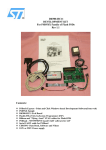
UM0044
User manual
FlashLINK JTAG programming cable for PSD and uPSD
Features
●
Allows PC or Notebook parallel port to program uPSD and PSD devices using PSDsoft
Express software development tool.
●
Supports IEEE 1149.1 JTAG signals (TCK, TMS, TDI, TDO).
●
Supports additional signals (TSTAT and TERR) to reduce programming time.
●
Single FlashLINK Cable assembly supports both 3.3V and 5V target devices with no
manual configuration. Target device may operate from 2.7V to 5.5V.
●
“Flying Lead” cable included to adapt to any target connector using 0.025” square
posts.
●
“LoopTest” cable included to validate PC parallel port operation.
Overview
The family of Flash PSD and uPSD devices offer In-System Programming (ISP) allowing a
completely blank device to be programmed while soldered to a circuit board. This simplifies
manufacturing and provides an effective way to update products after they are in use.
Flash PSD and uPSD devices comply to the core requirements of the IEEE 1149.1 JTAG
specification. However, these devices do not support boundary scan functions. Instead, they
support ISP, and some uPSD devices support emulation through JTAG.
The FlashLINK cable assembly shown in Figure 1 will perform ISP only on uPSD and PSD
devices, not memory or logic devices from other vendors. The software development tool
PSDsoft Express is a Windows based program which operates the FlashLINK cable
assembly (PSDsoft Express may be downloaded at no charge from www.st.com/psm).
PSDsoft Express supports device chaining, meaning more than one uPSD or PSD device
can reside in a single JTAG chain. Also, other devices (memory, logic from other vendors)
may reside in the JTAG chain, but these devices will stay in BYPASS Mode.
PSDsoft Express will generate BSDL, JAM STAPL, and SVF files for use with 3rd party
JTAG programming equipment.
The four basic JTAG pins (TCK, TMS, TDI, TDO) on uPSD devices are dedicated to operate
as JTAG pin at all times. However, the four JTAG pins on PSD devices may also be used for
general I/O functions.
ST has created two optional JTAG signals (TSTAT and TERR) to reduce programming
times. These pins supply programing status on signal pins rather than having to scan out the
status serially for each byte programmed in Flash memory. Program times using this method
(6-pin JTAG) can be as much as 30% less than the standard method (4-pin JTAG).
January 2007
Rev 5
1/15
www.st.com
www.BDTIC.com/ST
UM0044
Figure 1.
FlashLINK cable assembly
Mates
with
PC
parallel
port
Flying lead
cable
DB-25
Cable
FlashLINK
Adapter
12 WIRES
Target
device
6 feet
6 inches
DB-25 Cable, M-F
straight-through wiring
AI08862
1. 14-pin ribbon cable may also be used. Not supplied in FL-101 Kit.
2/15
www.BDTIC.com/ST
UM0044
Contents
Contents
1
Pin definition on FlashLINK adaptor . . . . . . . . . . . . . . . . . . . . . . . . . . . . 4
2
Connector definition . . . . . . . . . . . . . . . . . . . . . . . . . . . . . . . . . . . . . . . . . 5
3
Software . . . . . . . . . . . . . . . . . . . . . . . . . . . . . . . . . . . . . . . . . . . . . . . . . . . 6
3.1
4
5
Diagnostic tests . . . . . . . . . . . . . . . . . . . . . . . . . . . . . . . . . . . . . . . . . . . . . 6
3.1.1
Loop test . . . . . . . . . . . . . . . . . . . . . . . . . . . . . . . . . . . . . . . . . . . . . . . . . 6
3.1.2
Connect Test . . . . . . . . . . . . . . . . . . . . . . . . . . . . . . . . . . . . . . . . . . . . . . 6
Circuit examples . . . . . . . . . . . . . . . . . . . . . . . . . . . . . . . . . . . . . . . . . . . . 8
4.1
4-pin JTAG . . . . . . . . . . . . . . . . . . . . . . . . . . . . . . . . . . . . . . . . . . . . . . . . . 8
4.2
6-pin JTAG . . . . . . . . . . . . . . . . . . . . . . . . . . . . . . . . . . . . . . . . . . . . . . . . . 8
4.3
Multiplexed JTAG (PSD only) . . . . . . . . . . . . . . . . . . . . . . . . . . . . . . . . . . . 9
Chaining JTAG devices . . . . . . . . . . . . . . . . . . . . . . . . . . . . . . . . . . . . . . 11
Appendix A FlashLINK schematic. . . . . . . . . . . . . . . . . . . . . . . . . . . . . . . . . . . . . 12
6
Contact information . . . . . . . . . . . . . . . . . . . . . . . . . . . . . . . . . . . . . . . . 13
7
Revision history . . . . . . . . . . . . . . . . . . . . . . . . . . . . . . . . . . . . . . . . . . . 14
3/15
www.BDTIC.com/ST
Pin definition on FlashLINK adaptor
1
Pin definition on FlashLINK adaptor
Table 1.
Note:
UM0044
Pin description for 14-pin FlashLINK adaptor connector
Pin #
Signal
Name
1
JEN
2
Description
Type(1 FlashLINK is
)
Signal:
JTAG Enable - active-low when JTAG traffic is present
OC
Source
TRST(2)
JTAG Reset on target, active-low, optional per IEEE
1149.1
OC
Source
3
GND(3)
Signal Ground
4
(2)
CNTL
OC
Source
5
TDI
6
TSTAT
JTAG-ISP Programming Status to speed programming,
optional
7
VCC(4)
DC source from target, 2.7V to 5.5V
8
RST
Target system reset, recommended
9
TMS
JTAG IEEE 1149.1 Mode Select
10
GND
Signal Ground
11
TCK
JTAG IEEE 1149.1 Clock
12
GND
Signal Ground
13
TDO
JTAG IEEE 1149.1 Serial Data Out
Destination
14
TERR
JTAG-ISP Programming Error Status to speed
programming, optional
Destination
Generic Control signal
JTAG IEEE 1149.1 Serial Data Input
Source
Destination
OC
Source
Source
Source
1
OC = Open Collector, pulled-up to VCC inside FlashLINK Adaptor.
2
Not supported by PSDsoft Express, signals remain inactive.
3
All signal grounds are tied together inside FlashLINK Adaptor.
4
The target must supply VCC to the FlashLINK Adaptor (2.7V to 5.5VDC, 15mA max at 5.5V).
Not all 14 signals are required for all applications. Here is how they are used:
●
(6) Core signals that must be connected: TDI, TDO, TMS, TCK, VCC, GND
●
(2) Optional signals that reduce programming time as much as 30%: TSTAT and TERR
●
(1) Optional signal to control multiplexing of JTAG signals (PSD only) or to indicate
JTAG activity: JEN
●
(1) Optional IEEE-1149.1 signal for JTAG chain reset: TRST
●
(1) Optional (but recommended) signal to allow FlashLINK to reset target system after
ISP: RST
●
(1) Optional generic control signal to target system from FlashLINK: CNTL
●
(2) Two additional ground lines to help reduce EMI if a ribbon cable is used. These
ground lines “sandwich” the TCK signal in the ribbon cable. These two ground signals
are not present on the flying lead cable.
4/15
www.BDTIC.com/ST
UM0044
2
Connector definition
Connector definition
There is no industry standard JTAG connector. Each device manufacturer differs. ST has a
specific connector and pinout for the FlashLINK Adaptor. The connector scheme on the
FlashLINK connector can accept a standard 14-pin ribbon cable connector (2 rows of 7 pins
on 0.1” centers, standard keying) or any other user specific connector that can slide onto
0.025” square posts. The pinout for the FlashLINK Adaptor connector is shown in Figure 2.
A standard ribbon cable is a good way to quickly connect to the target circuit board. If a
ribbon cable is used, then the receiving connector on the target system should be the same
connector type with the same pinout as the FlashLINK Adaptor shown in Figure 2.
Note:
The JTAG signal TDI is sourced from the FlashLINK Adaptor and should be routed on the
target circuit board so that it connects to the TDI input pin of the PSD or uPSD device.
The JTAG signal TDO is an input received by the FlashLINK Adaptor and is sourced by the
PSD or uPSD device on its TDO output pin. See Figure 3 on page 8, Figure 4 on page 9,
and Figure 5 on page 10 for more information.
Figure 2.
Pinout for FlashLINK adaptor and target system JTAG connector
14
13
TERR TDO(1)
12
GND
11
TCK
10
GND
TMS
9
7
8
RST
6
TSTAT
KEY
WAY
VCC
5
TDI(2)
3
4
CNTL
GND
2
TRST
JEN
1
AI08867
Note:
This diagram perspective is looking into the face of the shrouded male connector on the
FlashLINK Adaptor, 0.025-inch (0.635mm) posts on 0.100-inch (2.54mm) centers.
Connector reference: Molex 70247-1401.
Recommended ribbon cables for quick connection of the FlashLINK Adaptor to the endproduct: Samtec HCSD-07-D-06.00-01-S-N; Digikey M3CCD-14065-ND.
Note:
1
TDO is a signal destination on the FlashLINK and a signal source on the target board.
2
TDI is a signal source on the FlashLINK and a signal destination on the target board.
5/15
www.BDTIC.com/ST
Software
3
UM0044
Software
The FlashLINK cable assembly is driven by the software development tool PSDsoft Express
(available at no charge from www.st.com/psm). With this tool you define the pin functions,
memory map, and PLD configuration of PSD or uPSD devices, add microcontroller firmware
to be programmed into Flash memory, then generate a single file to program into the device
(an object file with the filename extension *.obj). PSDsoft Express will then use the
FlashLINK cable assembly to program this object file into the PSD or uPSD device. Other
operations include erase, verify, upload, and blank check. See the PSDsoft Express User
Manual for more detail.
Note:
Be sure to use the latest version of PSDsoft Express. Updates are available from
www.st.com/psm.
3.1
Diagnostic tests
PSDsoft Express also performs some diagnostic tests for the PC parallel port and
FlashLINK cable assembly.
3.1.1
Loop test
Should be run first to test basic operation of the PC parallel port and the FlashLINK cable
assembly. “LoopTest” will wrap FlashLINK signal outputs back into FlashLINK signal inputs
for signal path verification.
3.1.2
Connect test
Is optional to test system performance and check the JTAG signal path all the way through
the target circuit board including PSD or uPSD device.
To run these tests, install and run PSDsoft Express on your PC or laptop:
1.
Connect the six foot long DB-25 cable to your PC parallel port on one side, and to the
FlashLINK Adaptor on the other side.
2.
Click mouse on the JTAG ISP programmer box at the bottom-left of the PSDsoft
Express main flow diagram.
3.
Select single or multiple JTAG devices depending on your target configuration (single is
most common), then click on the Hardware Setup (“HW Setup”) box at the lower part of
the JTAG Operations window.
For “LoopTest”:
1.
Connect the small loop test adaptor cable (not the flying lead cable) to the 14-pin
connector on the FlashLINK Adaptor.
2.
Connect the red lead of the loop test connector to a VCC source (5V or 3.3V), and
connect the black lead of the loop test connector to ground.
3.
In the “HW Setup” box click the “Loop Test” box to run the test. If it fails, be sure that
your are supplying VCC and ground, and also make sure that the PC’s parallel port is
enabled.
For “Connect Test”:
6/15
www.BDTIC.com/ST
UM0044
Software
1.
Connect the “Flying Lead” cable, or a ribbon cable to the FlashLINK Adaptor, and also
connect it to your target circuit board just as if you are ready to program the device.
2.
Turn on the power on the target device, and then click the “Connect Test” button in the
“HW Setup” box.
This test involves the circuit traces on your circuit board. If there is a failure, it is likely due to
signal routing or signal integrity on the target circuit board, or the PC may have compatibility
problems with the parallel port driver used by PSDsoft Express.
Note:
If either test fails, you will see a window pop-up that allows you to email in the problem.
Please do so and we will assist you.
7/15
www.BDTIC.com/ST
Circuit examples
UM0044
4
Circuit examples
4.1
4-pin JTAG
The first example shown in Figure 3 uses the standard JTAG signals (4-pin JTAG). This is
the default configuration in PSDsoft Express (4-pin JTAG).
Note:
The recommended pull-up resistors and decoupling capacitor are near the JTAG connector.
Figure 3.
Circuit example for 4-pin JTAG
SIGNAL
DIRECTION
DURING
JTAG
OPERATION
USER PC BOARD
100k
100k
100k
10k
100k
JTAG
CONN.
TMS - PC0
TMS
TCK - PC1
TCK
VSTBY or I/O - PC2
GENERAL I/O - PC3
GENERAL I/O - PC4
TDI - PC5
TDI
TDO - PC6
TDO
VCC (1)(2)
GENERAL I/O - PC7
JTAG
PROGRAMMING
OR TEST
EQUIPMENT
CONNECTS HERE
0.01
µF
µPSD or PSD Port C
GND
RST
USER I/O
SIGNALS
SYSTEM
RESET
CIRCUITY
(connect
directly to
RESET
Input on
µPSD)
AI08864b
Note:
4.2
1
For 5V uPSD3xxx devices, pull-up resistors and VCC pin on the JTAG connector should be
connected to 5V system VDD.
2
For 3.3V uPSD3xxx devices, pull-up resistors and VCC pin on the JTAG connector should be
connected to 3.3V system VCC.
6-pin JTAG
The second example in Figure 4 uses the two additional (and optional) JTAG signals TSTAT
and TERR to reduce programming time.
To configure this in PSDsoft Express, just click on pin PC3 or pin PC4 and choose
“Dedicated JTAG” function. These two signals must be used as a pair, so choosing either
one for JTAG will assign both to dedicated JTAG function.
8/15
www.BDTIC.com/ST
UM0044
Circuit examples
Figure 4.
Circuit example for 6-pin JTAG
100k Typ
10k
SIGNAL
DIRECTION
DURING
JTAG
OPERATION
USER PC BOARD
JTAG
CONN.
TMS - PC0
TMS
TCK - PC1
TCK
VSTBY or I/O - PC2
TSTAT - PC3(3)
TSTAT
TERR - PC4(3)
TERR
TDI - PC5
TDI
TDO - PC6
TDO
JTAG
PROGRAMMING
OR TEST
EQUIPMENT
CONNECTS HERE
VCC(1)(2)
GENERAL I/O - PC7
0.01
µF
µPSD or PSD Port C
GND
RST
USER I/O
SIGNALS
SYSTEM
RESET
CIRCUITY
(connect
directly to
RESET
Input on
µPSD)
AI08865b
Note:
4.3
1
For 5V uPSD3xxx devices, pull-up resistors and VCC pin on the JTAG connector should be
connected to 5V system VDD.
2
For 3.3V uPSD3xxx devices, pull-up resistors and VCC pin on the JTAG connector should be
connected to 3.3V system VCC.
3
TSTAT and TERR are not part of the IEEE 1149.1 Specification.
Multiplexed JTAG (PSD only)
The third example in Figure 5 illustrates one method to multiplex JTAG signals with general
I/O functions (PSD only, not available on uPSD). In this example, the PLD input pin at PC7
was chosen (this could be any PLD input pin) to control how the JTAG pins operate. The
signal JEN from the FlashLINK Adaptor drives PC7. When JEN is active (logic low), the
JTAG pins operate as JTAG. When JEN is inactive (logic high), the JTAG pins operate as
general I/O. You must configure this in PSDsoft Express by declaring the JTAG pins as
general I/O (not dedicated JTAG pins), then configure one PLD input pin (PC7 in this
example), then you must define an equation which will toggle the JTAG pin operation
between JTAG and general I/O.
To define this equation in PSDsoft Express:
1.
Click on the “JTAG Enable Tab” in the Design Assistant window.
2.
Write the equation for the internal node “jtagsel”, which controls the function of JTAG
pins (jtagsel logic high is JTAG, logic low is I/O).
For the example in Figure 5, the equation should be jtagsel = !PC7, so you would just have
to type !PC7 in the equations box and PSDsoft Express will do the rest.
Note:
You can click on the “Show Eq” button to see the resultant equation.
9/15
www.BDTIC.com/ST
Circuit examples
Note:
UM0044
JEN controls the tri-state buffers on the general I/O pins to avoid signal conflict when
operating in JTAG Mode or General I/O Mode.
Figure 5.
Circuit Example for Multiplexed JTAG pins (PSD only, not uPSD)
100k Typ
10k
SIGNAL
DIRECTION
DURING
JTAG
OPERATION
USER PC BOARD
JTAG
CONN.
TMS - PC0
TMS
TCK - PC1
TCK
VSTBY or I/O - PC2
TSTAT - PC3(3)
TSTAT
TERR - PC4(3)
TERR
TDI - PC5
TDI
TDO - PC6
TDO
JTAG
PROGRAMMING
OR TEST
EQUIPMENT
CONNECTS HERE
JEN
VCC (1)(2)
PLD INPUT - PC7
0.01
µF
PSD only (not µPSD) Port C
GND
JEN
RST
SYSTEM
RESET
CIRCUITY
MISC. USER I/O SIGNALS
(connect
directly to
RESET
Input on
µPSD)
AI08866b
Note:
1
For 5V uPSD3xxx devices, pull-up resistors and VCC pin on the JTAG connector should be
connected to 5V system VDD.
2
For 3.3V uPSD3xxx devices, pull-up resistors and VCC pin on the JTAG connector should be
connected to 3.3V system VCC.
3
TSTAT and TERR are not part of the IEEE 1149.1 Specification.
10/15
www.BDTIC.com/ST
UM0044
5
Chaining JTAG devices
Chaining JTAG devices
The IEEE-1149.1 specification allows chaining more than one device in a JTAG chain. uPSD
and PSD devices may be included in this JTAG chain. However, PSDsoft Express will place
devices from other vendors into BYPASS Mode, keeping them passive in the chain when
programming uPSD and PSD devices. Conversely, when other vendors’ JTAG control
software is operating the JTAG chain, uPSD and PSD devices may be placed into BYPASS
Mode. Figure 6 shows an example of a JTAG chain with three devices, including a device
from another manufacturer. This example also shows how to use 6-pin JTAG in a chaining
situation.
Chaining must be configured in PSDsoft Express:
Note:
1.
Click on the JTAG ISP box in the lower-left corner of the PSDsoft Express main flow
diagram.
2.
A pop-up dialog box will appear and ask how many devices are in the JTAG chain. If
you click “More than one,” you will go to the JTAG Operations window that allows you to
define the number of devices in the chain as well as their position.
If you do not see this dialog box (that asks how many devices are in the JTAG chain), pull
down the “Preferences” menu of the main PSDsoft Express window and re-enable this
option (question).
Figure 6.
Example of Chaining JTAG Devices
Target System, 3v or 5v
FlashLink
Adapter
Connector
VCC
TMS
TCK
7
7
9
9
11
11
TDI 5
1
TMS
TCK
5
6 optional
TSTAT
optional
!TERR 14
TDO 13
VCC
TDI
TDO
6
14
TSTAT
TERR\
PSD or uPSD
13
1 optional
2 optional
3
4 optional
8 recommended
!JEN
!TRST
(1)
GND
CNTL
!RST
(1) 10
GND
GND(1) 12
1
TMS
TCK
2
3
4
8
2
TDI
TDO
10
12
Any JTAG
Device in
ByPass Mode
TMS
TCK
straight-through
ribbon cable
2-row, 7-position
JTAG Chaining for PSD
or uPSD and other JTAGcompatible devices
n
TDI
TDO
System
Reset
Circuitry
TSTAT
TERR\
PSD or
uPSD
AI08863
Note:
1
All Ground pins are connected together inside the FlashLINK assembly.
11/15
www.BDTIC.com/ST
2
3
4
5
6
7
10
11
12
14
15
18
DB25-12P
J1
TCK
TMS
TDI
JEN
TRSTN
RSTN
TSTAT
VCC
TDO
CNTL
TERR
GND
R30
470
D10
LED
VCCA
DB25/2
DB25/3
DB25/4
DB25/5
DB25/6
DB25/7
DB25/10
DB25/11
DB25/12
DB25/14
DB25/15
DB25/18
PIN2
PIN3
PIN4
PIN5
PIN6
PIN7
PIN10
PIN11
PIN12
PIN14
PIN15
GND
R20
R21
R22
R23
R32
R31
R29
R28
R27
R26
R25
47
47
47
47
47
47
47
47
47
47
47
R2
470K
R5
4k7
VCC
C100
100P
6
3
4
Q1
9013
1
R6
4k7
C2
100P
R7
4k7
R11
10K
C4
100P
R1
470k
C3
100P
12/15
www.BDTIC.com/ST
4K7
R8
C1
100P
R9
10K
G
C5
100P
2
4
6
13
11
9
R10
10K
U2A
1
4
1N4148
D2
1
DM54ALS05A
3
U2B DM54ALS05A
5
U2C DM54ALS05A
12
U2F DM54ALS05A
10
U2E DM54ALS05A
8
U2D DM54ALS05A
9
Y1
7
Y2
5
Y3
3
Y4
1N4148
D1
C6
100P
74AC240
11
A1
13
A2
15
A3
17
A4
19
U1B
3
6
VCCA
Q2
9013
GND
G
R17
100K
12
Y4
14
Y3
16
Y2
18
Y1
R4
100K
VCC
R16
100K
74AC240
R15
100K
1
U1A
8
A4
6
A3
4
A2
2
A1
R19
10K
R33
10K
D4
6.2V
R18
10K
VCC
47
47
R39
47
R38
47
R37
47
R35
47
R34
47
R36
C10
105P
R43
R40
R41
4742
R
47
47
10
R14
JEN
TCK
TMS
TDI
1N5817
D3
TERR
TDO
TSTAT
CNTL
RSTN
TRSTN
R3
100K
VCC
JEN
GND
TDI
VCCA
TMS
TCK
TDO
VCC
2
4
6
8
10
12
14
C8
104P
HEADER 7X2
1
3
5
7
9
11
13
J2
C7
104P
TRSTN
CNTL
TSTAT
RSTN
GND
GND
TERR
Figure 7.
5
2
Appendix A
2
5
VCC
FlashLINK schematic
UM0044
FlashLINK schematic
FlashLINK adaptor schematic
UM0044
6
Contact information
Contact information
For current information on ST Flash PSD and uPSD products, please consult our pages on
the world wide web at www.st.com/psm
If you have questions or comments concerning the matters raised in this document, please
send them to: the following email address:
[email protected]
Please include your name, company, location, and phone number.
13/15
www.BDTIC.com/ST
Revision history
7
UM0044
Revision history
Table 2.
Document revision history
Date
Revision
Changes
1.0
First issue, written in WSI format
30-Jan-2002
1.1
Front page, and back two pages, in ST format, added to the PDF file
Any references to Waferscale, WSI, EasyFLASH and PSDsoft 2000
updated to ST, ST, Flash+PSD and PSDsoft Express
13-Nov-2003
2.0
Reformatted
09-Mar-2004
3.0
Republished
06-Sep-2005
4.0
Figure 3, Figure 4, Figure 5 updated by adding clearer JTAG
connection labeling
Notes associated with the above Figures renumbered
Figure 7 updated, connecting pin 13 to pin 8 for the DB25 connector
26-Jan-2007
5.0
Document reformatted
Figure 7 updated
14/15
www.BDTIC.com/ST
UM0044
Please Read Carefully:
Information in this document is provided solely in connection with ST products. STMicroelectronics NV and its subsidiaries (“ST”) reserve the
right to make changes, corrections, modifications or improvements, to this document, and the products and services described herein at any
time, without notice.
All ST products are sold pursuant to ST’s terms and conditions of sale.
Purchasers are solely responsible for the choice, selection and use of the ST products and services described herein, and ST assumes no
liability whatsoever relating to the choice, selection or use of the ST products and services described herein.
No license, express or implied, by estoppel or otherwise, to any intellectual property rights is granted under this document. If any part of this
document refers to any third party products or services it shall not be deemed a license grant by ST for the use of such third party products
or services, or any intellectual property contained therein or considered as a warranty covering the use in any manner whatsoever of such
third party products or services or any intellectual property contained therein.
UNLESS OTHERWISE SET FORTH IN ST’S TERMS AND CONDITIONS OF SALE ST DISCLAIMS ANY EXPRESS OR IMPLIED
WARRANTY WITH RESPECT TO THE USE AND/OR SALE OF ST PRODUCTS INCLUDING WITHOUT LIMITATION IMPLIED
WARRANTIES OF MERCHANTABILITY, FITNESS FOR A PARTICULAR PURPOSE (AND THEIR EQUIVALENTS UNDER THE LAWS
OF ANY JURISDICTION), OR INFRINGEMENT OF ANY PATENT, COPYRIGHT OR OTHER INTELLECTUAL PROPERTY RIGHT.
UNLESS EXPRESSLY APPROVED IN WRITING BY AN AUTHORIZED ST REPRESENTATIVE, ST PRODUCTS ARE NOT
RECOMMENDED, AUTHORIZED OR WARRANTED FOR USE IN MILITARY, AIR CRAFT, SPACE, LIFE SAVING, OR LIFE SUSTAINING
APPLICATIONS, NOR IN PRODUCTS OR SYSTEMS WHERE FAILURE OR MALFUNCTION MAY RESULT IN PERSONAL INJURY,
DEATH, OR SEVERE PROPERTY OR ENVIRONMENTAL DAMAGE. ST PRODUCTS WHICH ARE NOT SPECIFIED AS "AUTOMOTIVE
GRADE" MAY ONLY BE USED IN AUTOMOTIVE APPLICATIONS AT USER’S OWN RISK.
Resale of ST products with provisions different from the statements and/or technical features set forth in this document shall immediately void
any warranty granted by ST for the ST product or service described herein and shall not create or extend in any manner whatsoever, any
liability of ST.
ST and the ST logo are trademarks or registered trademarks of ST in various countries.
Information in this document supersedes and replaces all information previously supplied.
The ST logo is a registered trademark of STMicroelectronics. All other names are the property of their respective owners.
© 2007 STMicroelectronics - All rights reserved
STMicroelectronics group of companies
Australia - Belgium - Brazil - Canada - China - Czech Republic - Finland - France - Germany - Hong Kong - India - Israel - Italy - Japan Malaysia - Malta - Morocco - Singapore - Spain - Sweden - Switzerland - United Kingdom - United States of America
www.st.com
15/15
www.BDTIC.com/ST