1
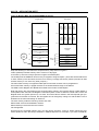
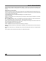
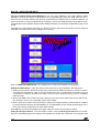
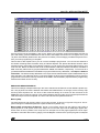
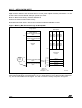
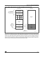
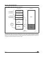
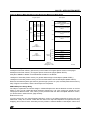
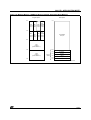
AN1178 APPLICATION NOTE 80C32/PSD8XX Design Guide CONTENTS ■ In-System Programming and In-Application reProgramming – The IAP Problem – A Common Solution ■ Physical Connections ■ Simple Design Example – Memory Map – PSDsoft Express Design Entry ■ Enhanced Design Example – Memory Map – PSDsoft Express Design Entry ■ Conclusion ■ References ■ Appendix A: Connecting to a PSD813F with no Boot Memory ™ EasyFLASH PSD8XX devices are members of a family of Flash memory-based peripherals for use with embedded microcontrollers (MCUs). These programmable system devices (PSDs) consist of memory, logic, and I/O. When coupled with a low-cost 80C32 MCU, the PSD forms a complete embedded Flash memory system that is 100% In-System Programmable (ISP) and In-Application Programmable (IAP). There are many features in the PSD silicon and in the PSDsoft Express development software that make ISP easy, regardless of how much experience you have with embedded design. This document offers two designs using a PSD813F1 and an Intel 80C32 MCU. Note that a variety of 8-bit MCU/MPUs can be used in place of the Intel part. Although the specifics of this document are based on the 80C32, this document can be used as a guide for other MCU/MPU applications. The first design is a simple system to get up and running quickly for basic applications or to check out your prototype 80C32 hardware. The second design illustrates the use of enhanced features of PSD In-System Programming as applied to the 80C32. You can start with the first design and migrate to the second as your functional requirements grow. There are other members of the PSD8XX family, including the PSD813F1/F3/F4/F5, the PSD833F2/834F2, and the PSD835G2. See the selector guide on the website for a comparison of the products. This application note is applicable to all PSD8XX family members. IN-SYSTEM PROGRAMMING AND IN-APPLICATION REPROGRAMMING Our industry uses the term In-System Programming (ISP) in a general sense. ISP is applicable to programmable logic, as well as programmable Non-Volatile Memory (NVM). However, an additional term will be used in this document: In-Application Programming (IAP). There are subtle yet significant differences between ISP and IAP when microcontrollers are involved. ISP of memory means that the MCU is off-line and not involved while memory is being programmed. For IAP, the MCU participates in programming the memory, which is important for systems that must be online while updating firmware. Often, ISP is well suited for manufacturing, while IAP is appropriate for field updates. PSD8XX devices are capable of both ISP and IAP. October 2001 1/25 AN1178 - APPLICATION NOTE Keep in mind that IAP can only program the memory sections of the PSD and not the configuration and programmable logic portions. With ISP, the entire PSD can be erased or programmed. The IAP Problem Typically, a host computer downloads firmware into an embedded Flash memory system through a communication channel that is controlled by the MCU. This channel is usually a UART, but any communication channel that the 80C32 supports will do. The 80C32 must execute the code that controls the IAP process from an independent memory array that is not being erased or programmed. Otherwise, boot code and Flash memory programming algorithms (IAP loader code) will be unavailable to the 80C32. It is absolutely necessary to use an alternate memory array (an independent memory that is not being programmed) to store the IAP loader code. A system designer must choose the type of alternate memory to store IAP loader code (ROM, SRAM, FLASH, or EEPROM); each type has advantages and disadvantages. This alternate memory may reside external to the MCU or on-chip. A top-level view of an embedded IAP flash system with external memory is shown in Figure 1. Figure 1. Embedded Flash System Capable of IAP (5 devices) Main Flash Memory 128 KBytes Host Computer Alternate Memory for ISP Loader Code 80C32 CPLD Communication Channel System SRAM 8 KBytes System I/O Embedded System AI03339B Another problem, which is specific to the 80C32 architecture, is related to the separate “Program” and “Data” address spaces. The 80C32 cannot write to Program space, but that is where the Flash memory resides that holds 80C32 firmware. How can one program Flash memory in-system if the 80C32 cannot write to program space? A Common Solution Without a PSD device, implementing IAP with the 80C32 can be difficult and time consuming. Philips’ application note AN440 contains a RAM loader program (bootstrap loader). It shows how to load code into an external RAM over a serial link after power-up and how to switch execution to that RAM to complete the boot sequence. This can be a cumbersome and error prone exercise using re-locatable code in volatile memory, which is difficult to debug, vulnerable to power outages, and not supported by all emulators. Additionally, this method restricts the designer to using a UART to implement IAP. To overcome the issue of Program versus Data space, a common practice is to combine the two address spaces, which reduces the total address space of the 80C32 by 50%. A Better, Integrated Solution Figure 2 shows a two-chip solution using an EasyFLASH PSD813F. This system has ample main Flash memory, a second alternate Flash memory to hold the IAP loader code and general data, and more SRAM. All three of these memories can operate independently and concurrently; meaning the MCU can operate from one memory while erasing/writing the other. This allows the MCU to continue normal oper- 2/25 AN1178 - APPLICATION NOTE ation during IAP, which is crucial for some applications. This system also has programmable logic, expanded I/O, and design security. The two chip solution is 100% programmable in the factory or in the field. Figure 2. Embedded Flash System Capable of ISP (2 devices) PSD813F Host Computer 80C32 Communication Channel 128 KByte Flash Optional 32 KByte EEPROM/Flash Optional 2KByte SRAM Programmable Logic I/O JTAG System I/O Embedded System AI03340B Note: 1. Other members of the PSD8XX family offer more Flash memory and more SRAM. 2. Only the PSD813F1 offers EEPROM, while the other members of the PSD8XX family offer secondary Flash memory. By design, the IAP method described above requires MCU participation to exercise a communication channel to implement a download to the main Flash memory. The PSD8XX also offers an alternative method called In-System Programming (ISP) to program the PSD using a built-in IEEE 1149.1 JTAG interface requiring no MCU participation. This means that a completely blank PSD can be soldered into place and the entire chip can be programmed in-system in just a few seconds using ST’s FlashLINK™ JTAG cable and PSDsoft Express development software. No 80C32 firmware needs to be written. Just plug in the FlashLINK cable to your PC’s parallel port and begin programming memory, logic, and configuration. This is a powerful feature of the PSD8XX that allows immediate development of application code in your lab, smart manufacturing techniques, and easy field updates. The FlashLINK™ cable and PSDsoft Express software are available in a kit from the website www.st.com/ psd. 3/25 AN1178 - APPLICATION NOTE Figure 3. Top Level Block Diagram of PSD813F PSD813F Device Security Optional 2 KByte SRAM Power Mngt CPLD 16 Output Macrocells 24 Input Macrocells JTAG Controller I/O Port A I/O Port B Optional 32 KByte EEPROM/Flash 4 sectors I/O Port C PLD Bus MCU Control Decode PLD 128 KByte Flash 8 sectors I/O Port D Page Reg I/O Bus MCU Address / Data MCU Address / Data / Control Bus AI03322B PHYSICAL CONNECTIONS Connect your 80C32 to the PSD8XX as shown in Figure 4 (next page). The same connections can be used for all of the members of the PSD8XX family except the PSD835G2, which has more I/O. The JTAG programming channel, SRAM with battery backup, LCD module, and MCU I/O connections are all optional. This example design is similar to ST’s DK900 Development kit, available for purchase on the web: www.st.com/psd. There are 13 unused PSD I/O pins in this example. Unused pins should be pulled to Vcc with a 100K resistor or tied to GND. See Application Note AN1153 for more information on the JTAG port. 4/25 AN1178 - APPLICATION NOTE Figure 4. Physical Connections, 80C32 and PSD813F AD7-AD0 DATA BUS U1 EA xx MHz XTAL1 XTAL2 INT0\ INT1\ UART PORT INT0 INT1 RXD TXD T0 T1 SPARE I/O P1.0 P1.1 P1.2 P1.3 P1.4 P1.5 P1.6 P1.7 2 X 16 LCD MODULE U2 AD0 AD1 AD2 AD3 AD4 AD5 AD6 AD7 AD0 AD1 AD2 AD3 AD4 AD5 AD6 AD7 A8 A9 A10 A11 A12 A13 A14 A15 A8 A9 A10 A11 A12 A13 A14 A15 WR RD PSEN RESET 39 40 41 42 43 44 45 46 WR\ RD\ PSEN\ 47 50 49 AS 10 ALE RST 30 31 32 33 34 35 36 37 RESET\ 48 ADIO0 ADIO1 ADIO2 ADIO3 ADIO4 ADIO5 ADIO6 ADIO7 PA0 PA1 PA2 PA3 PA4 PA5 PA6 PA7 ADIO8 ADIO9 ADIO10 ADIO11 ADIO12 ADIO13 ADIO14 ADIO15 PB0 PB1 PB2 PB3 PB4 PB5 PB6 PB7 CNTL0 CNTL1 CNTL2 PC0 PC1 PC2 PC3 PC4 PC5 PC6 PC7 PD0 RESET PD1 PD2 29 28 27 25 24 23 22 21 RWLCD RSLCD CSLCD 7 6 5 4 3 2 52 51 MCUIO0 MCUIO1 MCUIO2 MCUIO3 CSLCD 20 19 18 17 14 13 12 11 TMS TCK TSTAT TERR\ TDI TDO R/W RS E MCU I/O SIGNALS JTAG-ISP CONNECTOR 9 8 RESET RESET\ AI03341B SIMPLE DESIGN EXAMPLE The first design example outlines the steps required to get a 80C32 system up and running quickly. A connection diagram, memory map, and the necessary design file for the PSDsoft Express software development environment are provided. A PSD813F2 was used for this example. However, other members of the ™ Easy FLASH family may be used instead, with minor changes to the sample design file. See the selector guide on the website for a comparison of the products. Memory Map For this simple design, we used a PSD813F2 with the following memories: 128 Kbyte main Flash memory, broken into eight 16 Kbyte segments denoted fsi (i = 1-8) 32 Kbyte secondary Flash memory, broken into four 8 Kbyte segments denoted csbootj (j = 1-4). (The PSD813F1 has a boot EEPROM instead of Flash memory. Therefore, ees j (j = 1-4) would be used in place of csboot j.) 2 Kbyte SRAM (rs0) 256 byte PSD813F configuration register (csiop). Note: the PSD memory segments are defined in the “Chip Select Equations” screen in PSDsoft Express. We’ll use the boot memory to hold the ISP boot loader code, 80C32 interrupt vectors, and common firmware functions. For this example, we’ll execute from secondary Flash memory only and leave the main Flash memory in Data Space. Let’s examine the sample memory map in Figure 5, below: 5/25 AN1178 - APPLICATION NOTE Figure 5. Memory Map, Simple 80C32/PSD813F design Program Space Data Space FFFF FFFF FS1 FS3 FS5 FS7 Page 0 Page 1 Page 2 Page 3 16 KByte 16 KByte 16 KByte 16 KByte Unmapped C000 32 KBytes FS0 FS2 FS4 FS6 Page 0 Page 1 Page 2 Page 3 16 KByte 16 KByte 16 KByte 16 KByte 8000 8000 CSBOOT3/EES3 Optional Boot Flash/EEPROM 8 KBytes Unmapped 6000 22 KBytes CSBOOT2/EES2 Optional Boot Flash/EEPROM 8 KBytes Boot from Here 4000 2800 CSBOOT1/EES1 Optional Boot Flash/EEPROM 8 KBytes 2000 CSBOOT0/EES0 Optional Boot Flash/EEPROM Optional SRAM (RS0) 2 KBytes 2000 Not to Scale 8 KBytes 0000 Unmapped 0400 0300 LCD Chip Select (CSLCD) 256 Bytes PSD Control Register (CSIOP) 0200 0000 256 Bytes 8xC51 RAM AI03342B Keep the following in mind about the sample memory map shown in Figure 5: Yellow (shaded) indicates memory that is common to all pages. It is broken up into two 64 Kbyte spaces: Program and Data Space. The 32 Kbytes of the PSD813F boot memory is mapped to Program Space. (There are several references to “boot” memory in this document, but the “boot” memory is simply a secondary memory that can be used as boot memory or can serve any other purpose.) The main Flash memory is mapped to Data Space so that the contents can be programmed. All of main Flash memory is paged because of the limited address range of the 80C32. The PSD Control Register and SRAM are located at the bottom of Data Space. Note that placing the main Flash memory and secondary memory into Program Space or Data Space is accomplished with the PSD VM Register. PSDsoft Express is used to define the initial value of the VM Register when the system powers up or is reset. This initial value is stored in the fusemap that gets programmed into the PSD. At runtime, the VM register can be changed by writing to it with the MCU. This is illustrated in the enhanced design of Section 4. The boot memory holds the following vectors and code: 80C32 reset vector and initialization routines 80C32 interrupt vectors and service routines I/O management Since Figure 5 is a sample memory map, you may wish to change it. To do so, simply change the chip select equations within the Design Assistant in PSDsoft Express. For example, if you have a PSD813F 6/25 AN1178 - APPLICATION NOTE part that doesn’t contain the optional secondary memory, you will want to have the main Flash memory located in Program Space. See Appendix A for a sample memory map for parts with no secondary boot memory. PSDsoft Express Design Entry Highlights of design entry will be given here. Please refer to the PSDsoft Express User Manual for a thorough coverage of all the features of PSDsoft Express. This section is meant to show you just the essentials to get you going. Here are the steps: Invoke PSDsoft Express and Open a New Project. Start PSDsoft Express. Create a new project. Select your project folder and name the project (in this example, name the project “Easy8051” in the folder PSDsoft\my_project). MCU and PSD Selection. When you click OK in the “New Project” window, the “MCU and PSD Selection” screen appears. When you see this screen, make the following selections: Select an MCU manufacturer and part number. In this example, we’re using an Intel 8xC32. Notice how the control signals are selected for you in this case. Select the PSD8XX series for the PSD Family. Select a PSD813F2 and use the 52-pin PLCC package (J package). Based on the above selections, the “Bus Width”, “Bus Mode”, and “ALE/AS Active Level” will be set automatically. Set the main Flash memory to “Data Space Only” and the secondary Flash memory to “Program Space Only”. This is what the screen should look like after you’ve made the selections: 7/25 AN1178 - APPLICATION NOTE Now you have your project established based on a PSD813F2 and an 80C32. However, there are many other MCU/MPUs you could have chosen in place of the 80C32 and still have use of this document. Note that this template will work in our DK900 development kit. Click OK and the “Design Parameters” window will appear. Design Parameters . Choose “Use example template selection” and click OK to be taken to the “MCU Template Selection” screen. 8/25 AN1178 - APPLICATION NOTE MCU Template Selection. For the simple design, we will use paging, but will not be swapping memory locations. As such, you should pick “IAP, with memory paging” and click Generate to be taken to the “Pin Definitions” screen. Again, this template matches the requirements of the DK900 development kit. Pin Definitions. Your pin definitions should match the screen below and are setup according to the Physical Connections shown in Section 2. On this screen, you can add or update pin functionality as desired. Click Next >> to be taken to the “Design Assistant” screen. Note: there are detailed instructions on how to use this screen and other “Design Assistant” screens in the PSDsoft Express User Manual. 9/25 AN1178 - APPLICATION NOTE Page Register Definition. Looking at the memory map in Figure 5, we see that wee will need four memory pages, so we need to define two Page Register bits (22 = 4). Since you selected the template previously, the “Page Register Definition” should match the one shown below. Later, you will see how the Page Register can be used for general logic inputs to the PLD. Click Next >> when finished. 10/25 AN1178 - APPLICATION NOTE Chip Select Equations. Use this screen to enter chip-select equations to match your memory map. The chip select equations shown should match the memory map of Figure 5. Note the page number association for the fs0-7 segment selects. Click Next >> when finished. 11/25 AN1178 - APPLICATION NOTE I/O Logic and User Defined Node Equations. The “I/O Logic Equations” and “User Defined Node Equations” screens are used to enter equations for the registered logic within the PSD. Since this document focuses on issues related to ISP and IAP, registered logic equations are not covered. However, for more information on entering registered logic equations, refer to the PSDsoft Express User Manual. Also, see Application Note AN1356—Design Guide: PSDsoft Express, for a tutorial on implementing logic in the CPLD. Click Done and the software will check your design for errors (which there should be no errors using the template). You should now see the “Design Flow” window: Click on Additional PSD Settings in the “Design Flow” window and a dialog box will appear. Additional PSD Settings. There are three functions that can be accomplished in this dialog box: 1. Setting the security bit—blocks all access to the contents of the PSD’s memories by means of JTAG or a conventional programmer. That is, once the security bit is set, no programmer can read or copy the configuration or memory contents of the PSD. The only way to erase the security bit is to completely erase the PSD. 2. Specify the IEEE 1149.1 JTAG user code—allows you to enter a 32-bit code which can be used for various functions. Click on the “JTAG/ISP” tab for more details 3. Set the internal memories’ sector protections—allows the individual memory sectors within the PSD to be write protected to prevent accidental data loss. The MCU/MPU cannot change these settings at runtime; only a device programmer can alter these settings. Click OK and you will see the Design Flow again. Next, we need to fit the design to silicon. Fitting the Design to Silicon. To fit the design to silicon, click the Fit Design to Silicon box in the Design Flow. PSDsoft Express will compile and synthesize the design and create part of the program data 12/25 AN1178 - APPLICATION NOTE file (.obj) that will later be programmed into the PSD813F2 silicon. When this process is complete, a report will pop up that shows the resulting pin assignments PSD usage. This is the fitter report, which you can use to document your design. Since this design is based on a template, you should receive no errors during the fitting process. However, if you create a project from scratch and receive a Fitter error, you should check the PSDsoft Express User Manual for further instructions. C Code Generation. You can take advantage of the provided low-level C code for accessing memory elements within the PSD by clicking on the Generate C Code Specific to PSD box in the Design Flow window. To get the C functions and headers, specify the folder in which you want the ANSI C files to be written. ANSI C code functions and headers are generated for you to paste into your 80C32 C compiler environment in the folder you specify. Simply tailor the code to meet your system needs. See the PSDsoft Express User Manual for details on the C code generation feature. Merge MCU Firmware with PSD. Now that the fitting process is complete, PSDsoft Express has created a fuse pattern that reflects the PSD configuration and logic of your design. PSDsoft Express places this fuse information into a file (the .obj file). However this fuse pattern does not yet contain the 80C32 firmware. The next step will accomplish this, producing an .obj file that contains the PSD configuration and the 80C32 firmware. This final .obj file is what gets programmed into the PSD. The same .obj file is appended with MCU firmware in the next step below. For this step, “Merge MCU Firmware with PSD”, you will input the firmware file(s) that contain absolute addresses from your 80C32 compiler/linker in Intel Hex format. The Merger will map these file(s) into the memory segments of the PSD according to the chip select equations that you entered in the Design Assistant. This mapping process translates the absolute system addresses that 80C32 uses into physical internal PSD addresses that are used by a programmer to program the PSD. The address translation process is transparent. All you need to do is enter the file(s) that were generated from your 80C32 linker into the appropriate boxes and PSDsoft Express does the rest. Go to the design flow window and click the Merge MCU Firmware with PSD box. You should see the following warning as the utility starts: For this example, you can ignore this warning and click “OK” because we are only placing 80C32 code into Boot Flash memory segments csboot0 and csboot1, which are not paged. Here is an explanation of the warning in case you use paging in future designs: “PSDsoft Express attempts to populate all of the address range boxes for you, based on your chip select equations. These are the absolute address ranges that PSDsoft Express will expect to see inside the file(s) generated by your 80C32 linker. However, if PSDsoft Express sees that paging information is used in your PSD memory segment equations, PSDsoft Express warns you it has filled in address ranges that 13/25 AN1178 - APPLICATION NOTE may be ambiguous (overlapping or dependent on non-address signals, like page register bits) and it is up to you to resolve them. How you resolve them is purely a function of your 80C32 compiler/linker and how it handles paging. For example, some MCU linkers will generate a different file for each memory page of firmware, and each of these files will contain MCU addresses that do not exceed 16 bits. Other linkers will put all of the memory pages of firmware into a single file using MCU addresses greater than 16 bits to represent multiple pages (extends 16-bit addresses with page bits). Either method requires you to type the appropriate file name(s) and address ranges into the window based on how your particular 80C32 linker operates.” After clicking OK, you should see this: The far left column contains individual PSD memory segments. The next column shows the logic equations for selection of each memory segment (shown for reference only). In the middle are the address ranges that were specified in the “Chip Select Equations” screen to create the memory map. PSDsoft Express filled in these address fields for you. PSDsoft Express expects to find these absolute MCU addresses within your 80C32 linker file(s) when they are imported. On the right are boxes where you can type in (or browse for) the name of the file(s) (including path) that indicates the location of your 80C32 linker files. Notice that you can select Motorola S-Record or Intel Hex Record for the input type. Leave the “Mapping Mode” set to “Direct”. Now slide the scroll bar down until you see csboot0 and csboot1. 14/25 AN1178 - APPLICATION NOTE Type in the name of the file from your 80C32 linker that contains the firmware that will boot up your system. Click the Browse… button and go to the “Examples” directory and select “isp_8032.hex”. This file contains very simple 80C32 code that configures your DK900 system hardware and performs rudimentary tasks to check out your system. In this example, there are 16 Kbytes available in Boot Flash memory segments csboot0 and csboot1, which is more than enough for this simple boot and test code. After your new hardware is tested, you can add more code to the boot area for advanced tasks, such as implementing a download to main Flash memory from a host computer, as shown in the enhanced design of the next section. No file names are required for the main Flash memory regions (fs0-fs7) because we are only operating out of secondary Flash memory for now. Click OK, and the address translate process will produce the final programming data file (.obj) that can be used to program the PSD. Programming the PSD. The .obj file can be programmed into the PSD in one of three ways: The FlashLINK™ JTAG cable, which connects to the PC parallel port. The ST PSDpro device programmer, which also connects to the PC parallel port. Third-party programmers, such as Stag and Needhams. See the website at www.st.com/psd for a list of compatible third-party programmers. ™ First we’ll show you how to use the FlashLINK JTAG cable to program the PSD. ™ ™ Programming with FlashLINK . Connect the FlashLINK cable to your PC’s parallel port. Click the 15/25 AN1178 - APPLICATION NOTE ST JTAG/ISP box in the Design Flow window. You will be prompted for the number of devices in the JTAG chain on your circuit board. Make the appropriate selection and click OK. This document assumes only one device is in the JTAG chain. If you have more than one device, refer to the PSDsoft Express User Manual. For single device JTAG chains, the window will look similar to the following one: To use this window, ensure that the correct programming data file and PSD device appear in Step 1. For Step 2, select the desired operation, the regions of the PSD that the operation affects, and the number of JTAG pins (4 or 6) to use on the circuit board. The template assumes all six pins will be used. Before you perform the selected operation, click the Properties… button. This dialog box allows you to do the following: Set Port Pins: with this screen, you can set up the PSD’s I/O pins during JTAG operations. The default (except for the JTAG pins) is Input, which is usually fine for most pins. (Note that the PSD will not respond to any non-JTAG I/O.) However, sometimes it may be desirable to set a pin or pins to output during JTAG. For example, if you have chip-select signal being generated from the PSD that selects a device that potentially could drive signals on the JTAG lines (if you are multiplexing the pins), you would want that chipselect to be inactive during the JTAG operation. JTAG-ISP Attributes: this screen allows you to view the device name and Instruction Register length. This information may be useful to other design programs. User Code: basically, by clicking on the “User Code” tab, you are provided with a space to enter an IEEE 1149.1 User Code that will be compared to the value previously entered in the “Additional PSD Settings” screen. Once you are satisfied with your property settings, click OK to return to the “JTAG-ISP Operations” window. You can now perform the selected operation by clicking Execute. Before you leave this screen, you may wish to save your JTAG configuration. This can be done in Step 3 by clicking on the Save button and specifying a file name. This file can be used next time by clicking the Retrieve button. Programming with PSDpro. Ensure that the PSDpro device programmer is connected to your PC’s parallel port. Click on the ST Conventional Programmers box in the Design Flow window. You will see this: 16/25 AN1178 - APPLICATION NOTE If this is the first use of the PSDpro, click on the “Htest” icon to perform a test of the PSDpro and the PC port. After testing, place a PSD813F2 into the socket of the PSDpro and click on the “Program” icon. (The .obj file is automatically loaded when this process is invoked). The messaging of PSDsoft Express will inform you when programming is complete. This window is also helpful even if you do not have a PSDpro programmer. You can use this window to see where the Merge MCU Firmware utility of PSDsoft Express has placed the 80C32 firmware within physical memory of the PSD. For this design example, you can click on the secondary Flash memory icon in the tool bar. Notice the 80C32 reset vector at absolute MCU addresses 0000h and 0002h, translates to PSD secondary Flash memory physical addresses 20000h and 20002h, respectively. To see how all of your 80C32 absolute addresses translated into physical PSD memory addresses, click Report->Address Translation. The start and stop addresses in the report are the absolute MCU system addresses that you have specified. The addresses shown in square brackets are direct physical addresses used by a device programmer to access the memory elements of the PSD in a linear fashion (a special device programming mode that the MCU cannot access). ENHANCED DESIGN EXAMPLE This second design example builds upon the first to add enhanced features to this ISP/IAP capable system. The physical connections between the 80C32 and PSD813F2 do not change, but the memory map and chip select equations do. The focus of this enhanced design is to show how the memories of the PSD813F2 can be used concurrently. This means swapping the boot code out of Program Space after the initial boot sequence has completed. The boot code can then be updated if desired. Memory Map The boot sequence and memory swap is a four-step process, as shown in Figure 6 to Figure 9. The required changes in PSDsoft Express are explained after that (Section 4.2). Memory Map Configuration at Boot-Up. Figure 6 (next page) shows how the memory map looks at system power-on or at system reset. The “swap” bit is one of the eight internal PSD page register bits, whose value is zero by default. The “swap” bit is an example of how the page register bits can be implemented for uses other than memory paging. The VM Register controls which space (Program or Data) the 17/25 AN1178 - APPLICATION NOTE PSD memories appear in and can be set prior to runtime using PSDsoft Express Configuration. The VM register resides in the PSD and can be accessed at any time by the 80C32. (See the PSD8XX data sheets.) Here’s what the 80C32 does upon power-up or reset: Boot from Boot Flash memory csboot0 at address 0h Perform a checksum of main Flash memory Download main Flash memory from a host computer if needed and validate contents. Figure 6. Memory Map, Enhanced Design at Boot-Up/ISP Program Space Data Space FFFF FFFF CSBOOT3/EES3 Optional Boot Flash/EEPROM FS1 8 KBytes E000 FS3 FS5 FS7 Page 0 Page 1 Page 2 Page 3 16 KByte 16 KByte 16 KByte 16 KByte CSBOOT2/EES2 Optional Boot Flash/EEPROM 8 KBytes C000 C000 FS0 Unmapped FS2 FS4 FS6 Page 0 Page 1 Page 2 Page 3 32 KBytes 16 KByte 16 KByte 16 KByte 16 KByte 8000 Unmapped 22 KBytes Boot from Here 4000 2800 CSBOOT1/EES1 Optional Boot Flash/EEPROM 8 KBytes 2000 CSBOOT0/EES0 Optional Boot Flash/EEPROM 8 KBytes 0000 2000 Not to Scale Optional SRAM (RS0) 2 KBytes Unmapped 0400 0300 0200 0000 swap = 0 unlock = 0 VM Register = 12h LCD Chip Select (CSLCD) 256 Bytes PSD Control Register (CSIOP) 256 Bytes 8xC51 RAM AI03346B Memory Map Configuration After Moving the Main Flash. The next step is to move the main Flash memory from Data Space to Program Space. To do so, while executing out of the secondary Flash memory, write the value 06h to the VM register. You will now have the memory map shown in Figure 7. 18/25 AN1178 - APPLICATION NOTE Figure 7. Memory Map After Moving the Main Flash Memory to Program Space Program Space Data Space FFFF FFFF Boot Memory temporarily overlaps Flash segments FS1, FS3, FS5 and FS7 CSBOOT3/EES3 Optional Boot Flash/EEPROM 8 KBytes E000 CSBOOT2/EES2 Optional Boot Flash/EEPROM 8 KBytes C000 FS0 FS2 FS4 FS6 Unmapped Page 0 Page 1 Page 2 Page 3 54 KBytes 16 KByte 16 KByte 16 KByte 16 KByte 8000 Unmapped 16 KBytes Execute from Here 4000 2800 CSBOOT1/EES1 Optional Boot Flash/EEPROM 8 KBytes 2000 CSBOOT0/EES0 Optional Boot Flash/EEPROM 8 KBytes 0000 2000 Not to Scale Optional SRAM (RS0) 2 KBytes Unmapped 0400 0300 0200 0000 swap = 0 unlock = 0 VM Register = 06h LCD Chip Select (CSLCD) 256 Bytes PSD Control Register (CSIOP) 256 Bytes 8xC51 RAM AI03347B Memory Map Configuration After Setting the “swap” bit. Next, we want to swap main and secondary Flash memory and transfer execution to main Flash memory segment fs0. To do so, the “swap” bit must be set to HI to re-map the Boot Flash memory segments csboot0/csboot1 out of the MCU boot area and replace it with main Flash memory segment fs0, as shown in Figure 8. So that no program continuity is lost, the instruction that sets the “swap” bit is executed from csboot0 and the next contiguous instruction must be in fs0. For example, if the instruction that executes the swap is at location 1000h in csboot0, then fs0 must contain the next instruction to be executed at location 1002h. 19/25 AN1178 - APPLICATION NOTE Figure 8. Memory Map After Setting the “swap” bit Program Space Data Space FFFF FFFF Boot Memory temporarily overlaps Flash segments FS3, FS5 and FS7 CSBOOT3/EES3 Optional Boot Flash/EEPROM 8 KBytes E000 CSBOOT2/EES2 Optional Boot Flash/EEPROM 8 KBytes C000 Boot Memory temporarily overlaps Flash segments FS2, FS4 and FS6 CSBOOT1/EES1 Optional Boot Flash/EEPROM 8 KBytes Unmapped A000 48 KBytes CSBOOT0/EES0 Optional Boot Flash/EEPROM 8 KBytes 8000 Swap FS1 16 KBytes (Flash Sector 1) Execute from Here 4000 2800 2000 Optional SRAM (RS0) 2 KBytes Unmapped FS0 16 KBytes (Flash Sector 0) Not to Scale 0400 0300 0200 0000 0000 swap = 1 unlock = 0 VM Register = 06h LCD Chip Select (CSLCD) 256 Bytes PSD Control Register (CSIOP) 256 Bytes 8xC51 RAM AI03348B Memory Map Configuration After Moving the Boot Flash Memory to Data Space. The final step is to move the secondary Flash memory to Data Space so that it can be updated if desired. To move the secondary Flash memory to Data Space, write 0Ch to the VM register. Once the VM register has been written, you can program either half of the secondary Flash memory, depending on how the “unlock” bit is set. Figure 9 shows the final state of the memory map. 20/25 AN1178 - APPLICATION NOTE Figure 9. Memory Map After Moving the Boot Flash Memory to Data Space Program Space Data Space FFFF FFFF CSBOOT3/EES3 Optional Boot Flash/EEPROM FS3 FS5 FS7 8 KBytes E000 Page 1 Page 2 Page 3 C000 Not Mapped CSBOOT2/EES2 Optional Boot Flash/EEPROM 16 KByte 16 KByte 16 KByte 8 KBytes C000 CSBOOT1/EES1 Optional Boot Flash/EEPROM Page 0 FS2 FS4 FS6 8 KBytes Page 1 Page 2 Page 3 A000 16 KByte 16 KByte 16 KByte CSBOOT0/EES0 Optional Boot Flash/EEPROM 8 KBytes 8000 8000 Unmapped FS1 22 KBytes 16 KBytes (Flash Sector 1) 4000 2800 Optional SRAM (RS0) 2 KBytes 2000 Unmapped FS0 16 KBytes (Flash Sector 0) Not to Scale 0400 0300 LCD Chip Select (CSLCD) 256 Bytes PSD Control Register (CSIOP) 0200 0000 0000 256 Bytes 8xC51 RAM swap = 1 unlock = 0 or 1 VM Register = 0Ch AI03349B In this final configuration, the 80C32 has available: 32 Kbytes main Flash memory (fs0 and fs1) in the bottom of Program Space common to all pages 96 Kbytes main Flash memory in Program Space across three pages (8000h-FFFFh) 2 Kbytes of SRAM in addition to the SRAM that resides on the 80C32 16 Kbytes of secondary Flash memory for general data storage in Data Space (C000h-FFFFh) 16 Kbytes of secondary Flash memory for boot and ISP loader code in Data Space (8000h-FFFFh). Each time this 80C32 system gets reset or goes through a power-on cycle, the PSD presents the memory map of Figure 6 to the MCU, and the boot sequence is repeated. PSDsoft Express Design Entry The steps to implement the second design in PSDsoft Express are almost identical to those in the first design. In fact, you can repeat the steps outlined in Sections 3.2.1 to 3.2.3, except you should give your new project a different name. Then, when you are presented with the “MCU Template Selection” screen, you should select “Advanced IAP, page & swap”. Differences to note: You will notice that in the “Page Register Definition” screen in the Design Assistant, there are two new added bits: “swap” and “unlock”. These bits are used in the chip select equations to implement memory swapping and control of which secondary memory section is made available in Data Space. Notice how 21/25 AN1178 - APPLICATION NOTE these two bits are defined as logic inputs to the PLD instead of paging bits. The chip selects will now match the situational memory maps outlined in Figure 6 to Figure 9. That is, the memory map that is presented to the MCU varies dynamically based on the settings of the VM Register and Page Register bits “swap” and “unlock”. For more information on both the Page Register and VM Register, see the data sheets and the PSDsoft Express User Manual. When mapping the 80C32 firmware in the Address Translate utility of PSDsoft Express for this second design example, you still do not need to specify any Hex file for the PSD main Flash memory area. You only need to specify the 80C32 linker file(s) for the secondary Flash memory area (as in the first simple design) because the 80C32 will execute code from secondary Flash memory and download to main Flash memory. CONCLUSION ™ These examples are just two of an endless number of ways to configure the EasyFLASH PSD for your system. Concurrent memories with a built-in programmable decoder at the segment level offer excellent flexibility. Also, as you have seen with the “swap” and “unlock” bits, the page register bits do not have to be used just for paging through memory. The ability to expand your system does not require any physical connection changes, as everything is configured internal to the PSD. And finally, the JTAG channel can be used for ISP anytime, and anywhere, with no participation from the MCU. All of these features are crosschecked under the PSDsoft Express development environment to minimize your effort to design a Flash 80C32 system capable of ISP. REFERENCES PSD8XX Family Data Sheets for detailed PSD8XX information PSDsoft Express User Manual for details on how to use the design software Application Note AN1153—JTAG ISP Information: Flash PSD for detailed use of the JTAG port APPENDIX A: CONNECTING TO A PSD813F WITH NO BOOT MEMORY The following is a sample memory map for connecting to a PSD813F with no secondary memory (such as the PSD813F3 or PSD813F5). This memory map assumes you have downloaded the main Flash memory with the FlashLINK cable or you have booted from a separate PROM and have downloaded the Flash memory using the MCU. In either case, you must change your design to account for the lack of secondary memory. 22/25 AN1178 - APPLICATION NOTE Figure 10. Memory Map for a PSD813F Device (with No Secondary Boot Memory) Program Space Data Space FFFF FFFF Not FS3 FS5 FS7 Mapped Page 0 Page 1 Page 2 Page 3 16 KByte 16 KByte 16 KByte 16 KByte C000 Not FS2 FS4 FS6 Mapped Unmapped Page 0 Page 1 Page 2 Page 3 48 KBytes 16 KByte 16 KByte 16 KByte 16 KByte 8000 FS1 16 KBytes (Flash Sector 1) 4000 4000 2900 FS0 16 KBytes (Flash Sector 0) Not to Scale 2800 2000 5.75 KBytes PSD Control Register (CSIOP) 256 Bytes Optional SRAM (RS0) 2 KBytes Unmapped 0400 0000 Unmapped 0000 8xC51 RAM up to 1 KByte AI03350B 23/25 AN1178 - APPLICATION NOTE Table 1. Document Revision History Date Rev. Aug-2000 2.0 Document written in the WSI format 26-Oct-2001 3.0 Document converted to the ST format 24/25 Description of Revision AN1178 - APPLICATION NOTE For current information on PSD products, please consult our pages on the world wide web: www.st.com/psd If you have any questions or suggestions concerning the matters raised in this document, please send them to the following electronic mail addresses: [email protected] [email protected] (for application support) (for general enquiries) Please remember to include your name, company, location, telephone number and fax number. Information furnished is believed to be accurate and reliable. However, STMicroelectronics assumes no responsibility for the consequences of use of such information nor for any infringement of patents or other rights of third parties which may result from its use. No license is granted by implication or otherwise under any patent or patent rights of STMicroelectronics. Specifications mentioned in this publication are subject to change without notice. This publication supersedes and replaces all information previously supplied. STMicroelectronics products are not authorized for use as critical components in life support devices or systems without express written approval of STMicroelectronics. The ST logo is registered trademark of STMicroelectronics All other names are the property of their respective owners. 2001 STMicroelectronics - All Rights Reserved STMicroelectronics GROUP OF COMPANIES Australia - Brazil - China - Finland - France - Germany - Hong Kong - India - Italy - Japan - Malaysia - Malta - Morocco Singapore - Spain - Sweden - Switzerland - United Kingdom - U.S.A. www.st.com 25/25