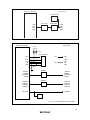
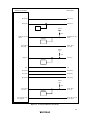
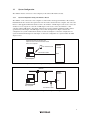
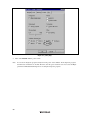
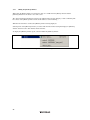
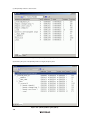
1
To our customers,
Old Company Name in Catalogs and Other Documents
On April 1st, 2010, NEC Electronics Corporation merged with Renesas Technology
Corporation, and Renesas Electronics Corporation took over all the business of both
companies. Therefore, although the old company name remains in this document, it is a valid
Renesas Electronics document. We appreciate your understanding.
Renesas Electronics website: http://www.renesas.com
April 1st, 2010
Renesas Electronics Corporation
Issued by: Renesas Electronics Corporation (http://www.renesas.com)
Send any inquiries to http://www.renesas.com/inquiry.
Notice
1.
2.
3.
4.
5.
6.
7.
All information included in this document is current as of the date this document is issued. Such information, however, is
subject to change without any prior notice. Before purchasing or using any Renesas Electronics products listed herein, please
confirm the latest product information with a Renesas Electronics sales office. Also, please pay regular and careful attention to
additional and different information to be disclosed by Renesas Electronics such as that disclosed through our website.
Renesas Electronics does not assume any liability for infringement of patents, copyrights, or other intellectual property rights
of third parties by or arising from the use of Renesas Electronics products or technical information described in this document.
No license, express, implied or otherwise, is granted hereby under any patents, copyrights or other intellectual property rights
of Renesas Electronics or others.
You should not alter, modify, copy, or otherwise misappropriate any Renesas Electronics product, whether in whole or in part.
Descriptions of circuits, software and other related information in this document are provided only to illustrate the operation of
semiconductor products and application examples. You are fully responsible for the incorporation of these circuits, software,
and information in the design of your equipment. Renesas Electronics assumes no responsibility for any losses incurred by
you or third parties arising from the use of these circuits, software, or information.
When exporting the products or technology described in this document, you should comply with the applicable export control
laws and regulations and follow the procedures required by such laws and regulations. You should not use Renesas
Electronics products or the technology described in this document for any purpose relating to military applications or use by
the military, including but not limited to the development of weapons of mass destruction. Renesas Electronics products and
technology may not be used for or incorporated into any products or systems whose manufacture, use, or sale is prohibited
under any applicable domestic or foreign laws or regulations.
Renesas Electronics has used reasonable care in preparing the information included in this document, but Renesas Electronics
does not warrant that such information is error free. Renesas Electronics assumes no liability whatsoever for any damages
incurred by you resulting from errors in or omissions from the information included herein.
Renesas Electronics products are classified according to the following three quality grades: “Standard”, “High Quality”, and
“Specific”. The recommended applications for each Renesas Electronics product depends on the product’s quality grade, as
indicated below. You must check the quality grade of each Renesas Electronics product before using it in a particular
application. You may not use any Renesas Electronics product for any application categorized as “Specific” without the prior
written consent of Renesas Electronics. Further, you may not use any Renesas Electronics product for any application for
which it is not intended without the prior written consent of Renesas Electronics. Renesas Electronics shall not be in any way
liable for any damages or losses incurred by you or third parties arising from the use of any Renesas Electronics product for an
application categorized as “Specific” or for which the product is not intended where you have failed to obtain the prior written
consent of Renesas Electronics. The quality grade of each Renesas Electronics product is “Standard” unless otherwise
expressly specified in a Renesas Electronics data sheets or data books, etc.
“Standard”:
8.
9.
10.
11.
12.
Computers; office equipment; communications equipment; test and measurement equipment; audio and visual
equipment; home electronic appliances; machine tools; personal electronic equipment; and industrial robots.
“High Quality”: Transportation equipment (automobiles, trains, ships, etc.); traffic control systems; anti-disaster systems; anticrime systems; safety equipment; and medical equipment not specifically designed for life support.
“Specific”:
Aircraft; aerospace equipment; submersible repeaters; nuclear reactor control systems; medical equipment or
systems for life support (e.g. artificial life support devices or systems), surgical implantations, or healthcare
intervention (e.g. excision, etc.), and any other applications or purposes that pose a direct threat to human life.
You should use the Renesas Electronics products described in this document within the range specified by Renesas Electronics,
especially with respect to the maximum rating, operating supply voltage range, movement power voltage range, heat radiation
characteristics, installation and other product characteristics. Renesas Electronics shall have no liability for malfunctions or
damages arising out of the use of Renesas Electronics products beyond such specified ranges.
Although Renesas Electronics endeavors to improve the quality and reliability of its products, semiconductor products have
specific characteristics such as the occurrence of failure at a certain rate and malfunctions under certain use conditions. Further,
Renesas Electronics products are not subject to radiation resistance design. Please be sure to implement safety measures to
guard them against the possibility of physical injury, and injury or damage caused by fire in the event of the failure of a
Renesas Electronics product, such as safety design for hardware and software including but not limited to redundancy, fire
control and malfunction prevention, appropriate treatment for aging degradation or any other appropriate measures. Because
the evaluation of microcomputer software alone is very difficult, please evaluate the safety of the final products or system
manufactured by you.
Please contact a Renesas Electronics sales office for details as to environmental matters such as the environmental
compatibility of each Renesas Electronics product. Please use Renesas Electronics products in compliance with all applicable
laws and regulations that regulate the inclusion or use of controlled substances, including without limitation, the EU RoHS
Directive. Renesas Electronics assumes no liability for damages or losses occurring as a result of your noncompliance with
applicable laws and regulations.
This document may not be reproduced or duplicated, in any form, in whole or in part, without prior written consent of Renesas
Electronics.
Please contact a Renesas Electronics sales office if you have any questions regarding the information contained in this
document or Renesas Electronics products, or if you have any other inquiries.
(Note 1) “Renesas Electronics” as used in this document means Renesas Electronics Corporation and also includes its majorityowned subsidiaries.
(Note 2) “Renesas Electronics product(s)” means any product developed or manufactured by or for Renesas Electronics.
User’s Manual
SH7058 E6000H
Emulator
User’s Manual
Renesas Microcomputer
Development Environment
System
SuperH™ Family / SH7050 Series
HS7058EPH60HE
Rev.6.00 2005.10
Keep safety first in your circuit designs!
1. Renesas Technology Corp. puts the maximum effort into making semiconductor products better and
more reliable, but there is always the possibility that trouble may occur with them. Trouble with
semiconductors may lead to personal injury, fire or property damage.
Remember to give due consideration to safety when making your circuit designs, with appropriate
measures such as (i) placement of substitutive, auxiliary circuits, (ii) use of nonflammable material or
(iii) prevention against any malfunction or mishap.
Notes regarding these materials
1. These materials are intended as a reference to assist our customers in the selection of the Renesas
Technology Corp. product best suited to the customer's application; they do not convey any license
under any intellectual property rights, or any other rights, belonging to Renesas Technology Corp. or
a third party.
2. Renesas Technology Corp. assumes no responsibility for any damage, or infringement of any thirdparty's rights, originating in the use of any product data, diagrams, charts, programs, algorithms, or
circuit application examples contained in these materials.
3. All information contained in these materials, including product data, diagrams, charts, programs and
algorithms represents information on products at the time of publication of these materials, and are
subject to change by Renesas Technology Corp. without notice due to product improvements or
other reasons. It is therefore recommended that customers contact Renesas Technology Corp. or
an authorized Renesas Technology Corp. product distributor for the latest product information
before purchasing a product listed herein.
The information described here may contain technical inaccuracies or typographical errors.
Renesas Technology Corp. assumes no responsibility for any damage, liability, or other loss rising
from these inaccuracies or errors.
Please also pay attention to information published by Renesas Technology Corp. by various means,
including the Renesas Technology Corp. Semiconductor home page (http://www.renesas.com).
4. When using any or all of the information contained in these materials, including product data,
diagrams, charts, programs, and algorithms, please be sure to evaluate all information as a total
system before making a final decision on the applicability of the information and products. Renesas
Technology Corp. assumes no responsibility for any damage, liability or other loss resulting from the
information contained herein.
5. Renesas Technology Corp. semiconductors are not designed or manufactured for use in a device or
system that is used under circumstances in which human life is potentially at stake. Please contact
Renesas Technology Corp. or an authorized Renesas Technology Corp. product distributor when
considering the use of a product contained herein for any specific purposes, such as apparatus or
systems for transportation, vehicular, medical, aerospace, nuclear, or undersea repeater use.
6. The prior written approval of Renesas Technology Corp. is necessary to reprint or reproduce in
whole or in part these materials.
7. If these products or technologies are subject to the Japanese export control restrictions, they must
be exported under a license from the Japanese government and cannot be imported into a country
other than the approved destination.
Any diversion or reexport contrary to the export control laws and regulations of Japan and/or the
country of destination is prohibited.
8. Please contact Renesas Technology Corp. for further details on these materials or the products
contained therein.
IMPORTANT INFORMATION
READ FIRST
• READ this user's manual before using this emulator product.
• KEEP the user's manual handy for future reference.
Do not attempt to use the emulator product until you fully understand its mechanism.
Emulator Product:
Throughout this document, the term "emulator product" shall be defined as the following
products produced only by Renesas Technology Corp. excluding all subsidiary products.
•
•
•
•
Emulator station
PC interface board
User system interface board
Cable
The user system or a host computer is not included in this definition.
Purpose of the Emulator Product:
This emulator product is a software and hardware development tool for systems employing the
Renesas microcomputer. This emulator product must only be used for the above purpose.
Limited Applications:
This emulator product is not authorized for use in MEDICAL, atomic energy, aeronautical or
space technology applications without consent of the appropriate officer of a Renesas sales
company. Such use includes, but is not limited to, use in life support systems. Buyers of this
emulator product must notify the relevant Renesas sales offices before planning to use the product
in such applications.
Improvement Policy:
Renesas Technology Corp. (including its subsidiaries, hereafter collectively referred to as
Renesas) pursues a policy of continuing improvement in design, performance, and safety of the
emulator product. Renesas reserves the right to change, wholly or partially, the specifications,
design, user's manual, and other documentation at any time without notice.
Target User of the Emulator Product:
This emulator product should only be used by those who have carefully read and thoroughly
understood the information and restrictions contained in the user's manual. Do not attempt to use
the emulator product until you fully understand its mechanism.
It is highly recommended that first-time users be instructed by users that are well versed in the
operation of the emulator product.
I
LIMITED WARRANTY
Renesas warrants its emulator products to be manufactured in
accordance with published specifications and free from defects in
material and/or workmanship. Renesas, at its option, will repair or
replace any emulator products returned intact to the factory,
transportation charges prepaid, which Renesas, upon inspection,
determine to be defective in material and/or workmanship. The
foregoing shall constitute the sole remedy for any breach of Renesas'
warranty. See the Renesas warranty booklet for details on the warranty
period. This warranty extends only to you, the original Purchaser. It is
not transferable to anyone who subsequently purchases the emulator
product from you. Renesas is not liable for any claim made by a third
party or made by you for a third party.
DISCLAIMER
RENESAS MAKES NO WARRANTIES, EITHER EXPRESS OR
IMPLIED, ORAL OR WRITTEN, EXCEPT AS PROVIDED
HEREIN, INCLUDING WITHOUT LIMITATION THEREOF,
WARRANTIES AS TO MARKETABILITY, MERCHANTABILITY,
FITNESS FOR ANY PARTICULAR PURPOSE OR USE, OR
AGAINST INFRINGEMENT OF ANY PATENT. IN NO EVENT
SHALL RENESAS BE LIABLE FOR ANY DIRECT, INCIDENTAL
OR CONSEQUENTIAL DAMAGES OF ANY NATURE, OR
LOSSES OR EXPENSES RESULTING FROM ANY DEFECTIVE
EMULATOR PRODUCT, THE USE OF ANY EMULATOR
PRODUCT, OR ITS DOCUMENTATION, EVEN IF ADVISED
OF THE POSSIBILITY OF SUCH DAMAGES. EXCEPT AS
EXPRESSLY STATED OTHERWISE IN THIS WARRANTY,
THIS EMULATOR PRODUCT IS SOLD "AS IS ", AND YOU
MUST ASSUME ALL RISK FOR THE USE AND RESULTS
OBTAINED FROM THE EMULATOR PRODUCT.
II
State Law:
Some states do not allow the exclusion or limitation of implied warranties or liability for
incidental or consequential damages, so the above limitation or exclusion may not apply to you.
This warranty gives you specific legal rights, and you may have other rights which may vary from
state to state.
The Warranty is Void in the Following Cases:
Renesas shall have no liability or legal responsibility for any problems caused by misuse,
abuse, misapplication, neglect, improper handling, installation, repair or modifications of the
emulator product without Renesas’ prior written consent or any problems caused by the user
system.
All Rights Reserved:
This user's manual and emulator product are copyrighted and all rights are reserved by
Renesas. No part of this user's manual, all or part, may be reproduced or duplicated in any form,
in hard-copy or machine-readable form, by any means available without Renesas' prior written
consent.
Other Important Things to Keep in Mind:
1. Circuitry and other examples described herein are meant merely to indicate the characteristics
and performance of Renesas' semiconductor products. Renesas assumes no responsibility for
any intellectual property claims or other problems that may result from applications based on
the examples described herein.
2. No license is granted by implication or otherwise under any patents or other rights of any third
party or Renesas.
Figures:
Some figures in this user's manual may show items different from your actual system.
Limited Anticipation of Danger:
Renesas cannot anticipate every possible circumstance that might involve a potential hazard.
The warnings in this user's manual and on the emulator product are therefore not all inclusive.
Therefore, you must use the emulator product safely at your own risk.
III
SAFETY PAGE
READ FIRST
• READ this user's manual before using this emulator product.
• KEEP the user's manual handy for future reference.
Do not attempt to use the emulator product until you fully understand its mechanism.
DEFINITION OF SIGNAL WORDS
This is the safety alert symbol. It is used to alert you to potential personal
injury hazards. Obey all safety messages that follow this symbol to avoid
possible injury or death.
DANGER
WARNING
CAUTION
CAUTION
DANGER indicates an imminently hazardous situation which, if not
avoided, will result in death or serious injury.
WARNING indicates a potentially hazardous situation which, if not
avoided, could result in death or serious injury.
CAUTION indicates a potentially hazardous situation which, if not
avoided, may result in minor or moderate injury.
CAUTION used without the safety alert symbol indicates a
potentially hazardous situation which, if not avoided, may result
in property damage.
NOTE emphasizes essential information.
IV
WARNING
Observe the precautions listed below. Failure to do so
will result in a FIRE HAZARD and will damage the user
system and the emulator product or will result in PERSONAL
INJURY. The USER PROGRAM will be LOST.
1. Carefully handle the emulator product to prevent
receiving an electric shock because the emulator product
has a DC power supply. Do not repair or remodel the
emulator product by yourself for electric shock
prevention and quality assurance.
2. Always switch OFF the emulator and user system before
connecting or disconnecting any CABLES or PARTS.
3. Always before connecting, make sure that pin 1 on both
sides are correctly aligned.
4. Supply power according to the power specifications and
do not apply an incorrect power voltage. Use only the
provided AC power cable. Use only the specified type of
fuse.
V
Warnings on Emulator Usage
Warnings described below apply as long as you use this emulator. Be sure to read and understand
the warnings below before using this emulator. Note that these are the main warnings, not the
complete list.
WARNING
Always switch OFF the emulator and user system before
connecting or disconnecting any CABLES or PARTS.
Failure to do so will result in a FIRE HAZARD and will
damage the user system and the emulator product or
will result in PERSONAL INJURY. The USER PROGRAM
will be LOST.
VI
CAUTION
Place the emulator station and evaluation chip board so
that the trace cables are not bent or twisted. A bent or
twisted cable will impose stress on the user interface
leading to connection or contact failure. Make sure that the
emulator station is placed in a secure position so that it
does not move during use nor impose stress on the user
interface.
E6000H
HITACHI
OK
E6000H
HITACHI
E6000H
HITACH
NG
I
NG
VII
CAUTION
This equipment has been tested and found to comply
with the limits for a Class A digital device, pursuant to part 15
of the FCC Rules. These limits are designed to provide
reasonable protection against harmful interference when the
equipment is operated in a commercial environment. This
equipment generates, uses, and can radiate radio frequency
energy and, if not installed and used in accordance with the
instruction manual, may cause harmful interference to radio
communications. Operation of this equipment in a residential
area is likely to cause harmful interference in which case the
user will be required to correct the interference at his own
expense.
VIII
Preface
Thank you for purchasing the E6000H emulator.
CAUTION
Read this manual before using the emulator product. Incorrect operation
or connection will damage the user system, the emulator product, and the
user program.
The E6000H emulator is an efficient software and hardware development support tool for application systems using the
microcomputer developed by Renesas Technology Corp.
The E6000H emulator can either be used without a user system, for developing and debugging software, or connected via
a user system interface cable to a user system, for debugging user hardware.
The emulator provides the following features:
1. Realtime emulation of the MCU
2. Efficient debugging enabled by variable break functions and a mass-storage trace memory (128-kcycles)
3. Parallel access with a command execution during emulation, for example
•
Trace data display
•
Emulation memory display and modification
4. Performance analysis
Measurement of subroutine execution time and count for evaluating the execution efficiency of user programs
®
5. Graphical User Interface by the High-performance Embedded Workshop that runs on Windows operating systems
High-performance Embedded Workshop is a Graphical User Interface intended to ease the development and debugging of
applications written in C/C++ programming language and assembly language. Its aim is to provide a powerful yet intuitive
way of accessing, observing and modifying the debugging platform in which the application is running.
High-performance Embedded Workshop is a powerful development environment for embedded applications targeted at
microcontrollers. The main features are:
• A configurable build engine that allows you to set-up compiler, assembler and linker options via an easy to use
interface.
• An integrated text editor with user customizable syntax coloring to improve code readability.
• A configurable environment to run your own tools.
• An integrated debugger which allows you to build and debug in the same application.
• Version control support.
The High-performance Embedded Workshop has been designed with two key aims; firstly to provide you, the user, with a
set of powerful development tools and, secondly, to unify and present them in a way that is easy to use.
i
About This Manual
This manual is comprised of two parts: Hardware Part and Debugger Part.
Hardware Part:
Preparation before use, hardware specifications, and troubleshooting procedure.
Debugger Part:
A peculiar debugging function to the emulator, tutorial, Emulator software specification, and
notes.
This manual describes the debugging function for SH7058 E6000H Emulator debugger that used with the Highperformance Embedded Workshop.
For detailed information on the basic “look and feel” of the High-performance Embedded Workshop and customizing the
High-performance Embedded Workshop environment and the build and the debugging functions common to the Highperformance Embedded Workshop products, refer to the High-performance Embedded Workshop user's manual.
This manual does not intend to explain how to write C/C++ or assembly language programs, how to use any particular
operating system or how best to tailor code for the individual devices. These issues are left to the respective manuals.
Microsoft, MS-DOS, Windows, Windows NT are registered trademarks of Microsoft Corporation.
Visual SourceSafe is a trademark of Microsoft Corporation.
IBM is a registered trademark of International Business Machines Corporation.
All brand or product names used in this manual are trademarks or registered trademarks of their respective companies or
organizations.
Document Conventions
This manual uses the following typographic conventions:
Table 1
Typographic Conventions
Convention
Meaning
[Menu->Menu Option]
Bold text with ‘->’ is used to indicate menu options
(for example, [File->Save As...]).
FILENAME.C
Uppercase names are used to indicate filenames.
“enter this string”
Used to indicate text that must be entered (excluding the “” quotes).
Key + Key
Used to indicate required key presses. For example, CTRL+N means
press the CTRL key and then, whilst holding the CTRL key down,
press the N key.
(The “how to” symbol)
When this symbol is used, it is always located in the left-hand margin.
It indicates that the text to its immediate right is describing “how to”
do something.
Components
Check all the components described in the component list unpacking. If the components are not complete, contact a
Renesas sales office.
ii
Contents
SH7058 Hardware Part
Section 1 Overview........................................................................................... 1
1.1
1.2
1.3
Notes on Usage .................................................................................................................1
Emulator Hardware Components ......................................................................................2
1.2.1 E6000H Station Components...............................................................................3
1.2.2 Evaluation Chip Board Configuration .................................................................5
1.2.3 Configuration of User System Interface Board....................................................6
System Configuration .......................................................................................................7
1.3.1 System Configuration Using a PC Interface Board..............................................7
Section 2
2.1
2.2
Section 3
3.1
3.2
3.3
3.4
3.5
Preparation before Use.................................................................... 9
Description on Emulator Usage ........................................................................................9
Emulator Connection ........................................................................................................10
2.2.1 Connecting the User System ................................................................................10
2.2.2 Connecting the User System Interface Board ......................................................11
2.2.3 Connecting the External Probe.............................................................................12
2.2.4 Selecting the Clock ..............................................................................................13
2.2.5 Connecting the System Ground ...........................................................................15
2.2.6 PC Interface Board Specifications .......................................................................16
Hardware Specifications ................................................................. 17
Environmental Conditions ................................................................................................17
Emulator External Dimensions and Mass .........................................................................18
User System Interface Circuit ...........................................................................................19
3.3.1 User System Interface Circuit ..............................................................................19
3.3.2 Delay Time with the User System Interface ........................................................26
Connecting the Emulator to the User System ...................................................................26
3.4.1 Connecting to the User System ............................................................................26
3.4.2 Pin Assignment on the User System Interface Connector....................................36
3.4.3 Precautions on Connecting the User System........................................................44
Support of the Target MCU ..............................................................................................45
3.5.1 Memory Space .....................................................................................................45
3.5.2 Low Power-Consumption Mode
(Sleep, Software Standby, and Hardware Standby)..............................................46
3.5.3 Interrupts ..............................................................................................................46
3.5.4 Control Input Signals (_RES, _BREQ, and _WAIT)...........................................46
3.5.5 Watchdog Timer (WDT)......................................................................................46
3.5.6 A/D Converter......................................................................................................47
3.5.7 Emulator State and On-Chip Modules .................................................................47
3.5.8 Different Initial Values of Registers in the Emulator...........................................48
Section 4 Diagnostic Test Procedure ................................................................ 49
4.1
4.2
4.3
System Set-Up for Diagnostic Program Execution ...........................................................49
Test Item of the Diagnostic Program ................................................................................51
Diagnostic Test Procedure Using the Diagnostic Program ...............................................52
iii
SH7059 Hardware Part
Section 1 Overview ...........................................................................................1
1.1
1.2
1.3
Notes on Usage ................................................................................................................. 1
Emulator Hardware Components ...................................................................................... 2
1.2.1 E6000H Station Components............................................................................... 3
1.2.2 Evaluation Chip Board Configuration ................................................................. 5
1.2.3 Configuration of User System Interface Board.................................................... 6
System Configuration ....................................................................................................... 7
1.3.1 System Configuration Using a PC Interface Board ............................................. 7
Section 2
2.1
2.2
Section 3
3.1
3.2
3.3
3.4
3.5
Preparation before Use ....................................................................9
Description on Emulator Usage ........................................................................................ 9
Emulator Connection ........................................................................................................ 10
2.2.1 Connecting the User System ................................................................................ 10
2.2.2 Connecting the User System Interface Board ...................................................... 11
2.2.3 Connecting the External Probe ............................................................................ 12
2.2.4 Selecting the Clock .............................................................................................. 13
2.2.5 Connecting the System Ground ........................................................................... 15
2.2.6 PC Interface Board Specifications ....................................................................... 16
Hardware Specifications..................................................................17
Environmental Conditions ................................................................................................ 17
Emulator External Dimensions and Mass ......................................................................... 18
User System Interface Circuit ........................................................................................... 19
3.3.1 User System Interface Circuit .............................................................................. 19
3.3.2 Delay Time with the User System Interface ........................................................ 26
Connecting the Emulator to the User System ................................................................... 26
3.4.1 Connecting to the User System............................................................................ 26
3.4.2 Pin Assignment on the User System Interface Connector ................................... 36
3.4.3 Precautions on Connecting the User System ....................................................... 44
Support of the Target MCU .............................................................................................. 45
3.5.1 Memory Space ..................................................................................................... 45
3.5.2 Low Power-Consumption Mode
(Sleep, Software Standby, and Hardware Standby).............................................. 46
3.5.3 Interrupts.............................................................................................................. 46
3.5.4 Control Input Signals (_RES, _BREQ, and _WAIT)........................................... 46
3.5.5 Watchdog Timer (WDT)...................................................................................... 46
3.5.6 A/D Converter...................................................................................................... 47
3.5.7 Emulator State and On-Chip Modules ................................................................. 47
3.5.8 Different Initial Values of Registers in the Emulator .......................................... 48
Section 4 Diagnostic Test Procedure.................................................................49
4.1
4.2
4.3
iv
System Set-Up for Diagnostic Program Execution........................................................... 49
Test Item of the Diagnostic Program ................................................................................ 51
Diagnostic Test Procedure Using the Diagnostic Program ............................................... 52
Debugger Part
Section 1 Overview........................................................................................... 1
Section 2 Preparation before Use...................................................................... 3
2.1
2.2
2.3
2.4
Method for Activating High-performance Embedded Workshop.....................................3
2.1.1 Creating a New Workspace (Toolchain Not Used)..............................................4
2.1.2 Creating a New Workspace (Toolchain Used) .......................................................8
2.1.3 Selecting an Existing Workspace ...........................................................................12
Connecting the Emulator...................................................................................................13
Re-connecting the Emulator..............................................................................................14
Ending the Emulator .........................................................................................................14
Section 3 Debugging......................................................................................... 15
3.1
3.2
3.3
3.4
3.5
3.6
3.7
3.8
Setting the Environment for Emulation ............................................................................15
3.1.1 Opening the [Configuration Properties] Dialog Box ...........................................15
3.1.2 Using the Emulation RAM ..................................................................................18
3.1.3 Selecting the Interface to be Connected...............................................................20
Downloading a Program ...................................................................................................21
3.2.1 Downloading a Program ......................................................................................21
3.2.2 Viewing the Source Code ....................................................................................21
3.2.3 Viewing the Assembly-Language Code...............................................................24
3.2.4 Modifying the Assembly-Language Code ...........................................................25
3.2.5 Viewing a Specific Address .................................................................................25
3.2.6 Viewing the Current Program Counter Address ..................................................25
Viewing the Current Status ...............................................................................................26
Reading and Displaying the Emulator Information Regularly..........................................27
3.4.1 Opening the [Extended Monitor] Window...........................................................27
3.4.2 Selecting Items to be Displayed...........................................................................28
Displaying Memory Contents in Realtime........................................................................29
3.5.1 Opening the [Monitor] Window...........................................................................29
3.5.2 Changing the Monitor Settings ............................................................................31
3.5.3 Temporarily Stopping Update of the Monitor......................................................31
3.5.4 Deleting the Monitor Settings ..............................................................................31
3.5.5 Monitoring Variables ...........................................................................................31
3.5.6 Hiding the [Monitor] Window .............................................................................32
3.5.7 Managing the [Monitor] Window ........................................................................33
Looking at Variables .........................................................................................................34
3.6.1 [Watch] Window..................................................................................................34
Using the Event Points ......................................................................................................36
3.7.1 Setting a Software Breakpoint .............................................................................37
3.7.2 Setting an On-Chip Breakpoint............................................................................39
3.7.3 Settings an On-Emulator Breakpoint ...................................................................42
3.7.4 Editing Event Points ............................................................................................45
3.7.5 Modifying Event Points .......................................................................................45
3.7.6 Enabling an Event Point.......................................................................................45
3.7.7 Disabling an Event Point......................................................................................45
3.7.8 Deleting an Event Point .......................................................................................45
3.7.9 Deleting All Event Points ....................................................................................45
3.7.10 Viewing the Source Line for an Event Point........................................................45
Viewing the Trace Information .........................................................................................46
3.8.1 Opening the [Trace] Window ..............................................................................46
v
3.8.2 Acquiring Trace Information ............................................................................... 46
3.8.3 Specifying Trace Acquisition Conditions ............................................................ 48
3.8.4 Searching for a Trace Record............................................................................... 55
3.8.5 Clearing the Trace Information............................................................................ 56
3.8.6 Saving the Trace Information in a File ................................................................ 57
3.8.7 Viewing the [Editor] Window.............................................................................. 57
3.8.8 Trimming the Source ........................................................................................... 57
3.8.9 Temporarily Stopping Trace Acquisition............................................................. 57
3.8.10 Restarting Trace Acquisition ............................................................................... 57
3.8.11 Extracting Records from the Acquired Information ............................................ 58
3.8.12 Calculating the Difference in Time Stamping ..................................................... 60
3.8.13 Analyzing Statistical Information ........................................................................ 61
3.8.14 Extracting Function Calls from the Acquired Trace Information ........................ 62
3.9 Analyzing Performance..................................................................................................... 63
3.9.1 Opening the [Performance Analysis] Window .................................................... 65
3.9.2 Setting Conditions for Measurement ................................................................... 66
3.9.3 Starting Performance Data Acquisition ............................................................... 73
3.9.4 Deleting a Measurement Condition ..................................................................... 73
3.9.5 Deleting All Measurement Conditions ................................................................ 73
3.10 Profiling Function ............................................................................................................. 74
3.10.1 Enabling the Profile ............................................................................................. 74
3.10.2 Specifying Measuring Mode................................................................................ 74
3.10.3 Executing the Program and Checking the Results ............................................... 74
3.10.4 [List] Sheet........................................................................................................... 75
3.10.5 [Tree] Sheet.......................................................................................................... 76
3.11 [Profile-Chart] Window .................................................................................................... 78
Section 4
4.1
4.2
4.3
Tutorial ............................................................................................81
Introduction....................................................................................................................... 81
Running the High-performance Embedded Workshop ..................................................... 82
Downloading the Tutorial Program .................................................................................. 83
4.3.1 Downloading the Tutorial Program ..................................................................... 83
4.3.2 Displaying the Source Program ........................................................................... 84
4.4 Setting a Software Breakpoint ............................................................................................. 85
4.5 Setting Registers .................................................................................................................. 86
4.6 Executing the Program......................................................................................................... 87
4.7 Reviewing Breakpoints........................................................................................................ 90
4.8 Referring to Symbols ........................................................................................................... 91
4.9 Viewing Memory................................................................................................................. 92
4.10 Watching Variables ........................................................................................................... 93
4.11 Displaying Local Variables ............................................................................................... 96
4.12 Stepping Through a Program ............................................................................................. 97
4.12.1 Executing the [Step In] Command ....................................................................... 97
4.12.2 Executing the [Step Out] Command .................................................................... 99
4.12.3 Executing the [Step Over] Command .................................................................. 100
4.13 Forced Breaking of Program Executions ........................................................................... 101
4.14 Resetting the Target MCU ................................................................................................. 101
4.15 Break Function................................................................................................................... 102
4.15.1 Software Break Function...................................................................................... 102
4.15.2 On-Chip Break Function ...................................................................................... 108
4.16 Trace Functions ................................................................................................................. 110
4.16.1 Displaying Trace Information by the Free Trace Function .................................. 111
4.16.2 Displaying Trace Information by the Trace Stop Function.................................. 113
vi
4.17
4.18
4.19
4.20
4.21
4.16.3 Displaying Trace Information by the Conditional Trace Function ......................116
4.16.4 Statistics ...............................................................................................................117
4.16.5 Function Calls ......................................................................................................121
Stack Trace Function .........................................................................................................122
Performance Analysis Function .........................................................................................124
4.18.1 Time Of Specified Range Measurement ..............................................................124
Profiling Function ..............................................................................................................127
Monitor Function ...............................................................................................................132
What Next? ........................................................................................................................134
Section 5 Software Specifications and Notes Specific to This Product............ 135
5.1
5.2
5.3
Supported Hardware .........................................................................................................135
Debugging Platform ..........................................................................................................135
Displaying and Modifying the Contents of Memory ........................................................135
5.3.1 Reference Values for Parallel Access Function Termination Period ...................136
5.3.2 Monitor Function .................................................................................................137
5.3.3 Note on Accessing Memory.................................................................................137
5.4 Executing Your Program...................................................................................................137
5.4.1 Step Execution .....................................................................................................137
5.4.2 Break Suspension.................................................................................................137
5.5 Event Functions.................................................................................................................138
5.5.1 Software Breakpoints...........................................................................................138
5.5.2 On-Chip Break .....................................................................................................138
5.5.3 On-Emulator Break..............................................................................................139
5.6 Trace Functions.................................................................................................................140
5.6.1 Displaying the Trace Information ........................................................................140
5.6.2 Specifying Trace Acquisition Conditions ............................................................140
5.6.3 Searching for a Trace Record...............................................................................140
5.6.4 Filtering Trace Records........................................................................................140
5.7 Monitor Function ..............................................................................................................140
5.8 Performance Analysis Function ........................................................................................141
5.8.1 Errors ...................................................................................................................141
5.8.2 Notes ....................................................................................................................141
5.9 Profiling Function .............................................................................................................142
5.10 Input Format......................................................................................................................143
5.10.1 Entering Masks ....................................................................................................143
5.11 Downloading a Program ...................................................................................................143
5.12 Tutorial Program ...............................................................................................................144
5.12.1 Downloading the Tutorial Program .....................................................................144
5.12.2 Notes on Operating the Tutorial Program ............................................................144
Section 6 Error Messages.................................................................................. 145
6.1
Error Messages of the Emulator........................................................................................145
6.1.1 Error Messages at Emulator Initiation .................................................................145
6.1.2 Error Messages during Emulation........................................................................147
Appendix A Menus ........................................................................................... 149
Appendix B Command Lines............................................................................ 153
vii
viii
SH7058 Hardware Part
Section 1 Overview
1.1
Notes on Usage
CAUTION
READ the following warnings before using the emulator product.
Incorrect operation will damage the user system and the emulator
product. The USER PROGRAM will be LOST.
1. Check all components with the component list after unpacking the emulator.
2. Never place heavy objects on the casing.
3. Observe the following conditions in the area where the emulator is to be used:
•
Make sure that the internal cooling fans on the sides of the emulator must be at least 20 cm (8") away
from walls or other equipment.
•
Keep out of direct sunlight or heat. Refer to section 3.1, Environmental Conditions.
•
Use in an environment with constant temperature and humidity.
•
Protect the emulator from dust.
•
Avoid subjecting the emulator to excessive vibration. Refer to section 3.1, Environmental Conditions.
4. Protect the emulator from excessive impacts and stresses.
5. Before using the emulator's power supply, check its specifications such as power voltage and frequency.
6. When moving the emulator, take care not to vibrate or otherwise damage it.
7. After connecting the cable, check that it is connected correctly. For details, refer to section 2, Preparation
before Use.
8. Supply power to the emulator and connected parts after connecting all cables. Cables must not be connected
or removed while the power is on.
9. For details on differences between the target MCU and the emulator, refer to section 3.5, Support of the
Target MCU.
1
1.2
Emulator Hardware Components
The emulator consists of an E6000H station and an evaluation chip board. By installing a user system interface
board (option) on your host computer, the emulator can be connected in the same package as the device. PC
interface (option) includes a PC interface board (PCI bus and PC card bus), a LAN adapter (connected with the
network), and a USB adapter (connected with the USB interface). By connecting the emulator to the host
computer via those interfaces, the High-performance Embedded Workshop can be used for debugging. For
details on PC interface boards (available for PCI bus and PC card bus specifications), LAN adapter, and USB
adapter, refer to their description notes.
USB adapter
(option)
USB cable
(option)
PC
PC interface cable
(option)
PC interface
cable (option)
Network
LAN adapter
(option)
PC interface cable (option)
PC interface board (option)
E6000H
RENESAS
E6000H station
Evaluation chip board
User system
interface board
IC socket
User system
Figure 1.1 Emulator Hardware Components
2
1.2.1
E6000H Station Components (A Part of Photos may be Different from Real Appearances)
The names of the components on the front/rear panel of the E6000H station are listed below.
Front Panel:
Figure 1.2 E6000H Station: Front Panel
(a) POWER lamp:
Is lit up while the E6000H station is supplied with power.
(b) RUN lamp:
Is lit up while the user program is running.
3
Rear Panel:
Figure 1.3 E6000H Station: Rear Panel
(a)
Power switch:
Turning this switch to I (input) supplies power to
the emulator (E6000H station and evaluation chip
board).
(b)
AC power connector:
For an AC 100-V to 240-V power supply.
(c)
PC interface cable connector:
For the PC interface cable that connects the
host computer to the E6000H station. A PC
interface board, PC card interface, LAN adapter,
or USB adapter can be connected. Marked PC/IF.
4
1.2.2
Evaluation Chip Board Configuration
The names of the components on the evaluation chip board of the emulator are listed below.
Figure 1.4 Evaluation Chip Board
(a) Station to evaluation chip board
interface connector cover:
This is a cover for protecting the connector that
connects the E6000H station to the evaluation chip
board.
(b) Crystal oscillator terminals:
For installing a crystal oscillator to be used as
an external clock source for the target MCU.
(c) HS7058PWB20H board:
Connector to the trace cable is attached.
(d) HS7058PWB30H board:
An evaluation chip is installed and a dedicated
connector to the user system interface board or
user system is attached.
(e) User system interface board
connector:
For connecting the user system interface board or
user system.
Note: (a) to (e) listed above are referred to as the evaluation chip board.
5
1.2.3
Configuration of User System Interface Board
The names of the components of the user system interface board are given below.
Figure 1.5 Configuration of User System Interface Board
(a) Connector for the evaluation chip
board:
For connection to the evaluation chip board.
(b) Connector for the user system:
For connection to the user system.
6
1.3
System Configuration
The emulator must be connected to a host computer (via the selected PC interface board).
1.3.1
System Configuration Using a PC Interface Board
The emulator can be connected to a host computer via a PC interface board (option: PCI bus or PC card bus).
Install the PC interface board to the expansion slot for the interface board in the host computer, and connect the
interface cable supplied with the PC interface board to the emulator. A LAN adapter can be used to connect the
emulator to a host computer as a network. A USB adapter can be used to connect the emulator to a host
computer with the USB interface. For details on PC interface boards (available for PCI bus and PC card bus
specifications), LAN adapter, and USB adapter, refer to their description notes. Figure 1.6 shows the
configuration of a system in which the PC interface board is used. Figure 1.7 shows the configuration of a
system in which the LAN adapter is used. Figure 1.8 shows the configuration of a system in which the USB
adapter is used.
Install the PC interface board to the
expansion slot for the PC interface board
in the host computer.
PC interface board
E6000H
emulator
PC interface cable
PCIF
Host computer
Figure 1.6 System Configuration Using a PC Interface Board
Network
E6000H
emulator
PCIF
LAN adapter
Host computer
PC interface cable
Figure 1.7 System Configuration Using a LAN Adapter
7
E6000H
emulator
PCIF
USB adapter
Host computer
USB
Figure 1.8 System Configuration Using a USB Adapter
8
Section 2 Preparation before Use
2.1
Description on Emulator Usage
This section describes the preparation before use of the emulator. Figure 2.1 is a flowchart on preparation before
debugging with the emulator.
CAUTION
Read this section and understand its contents before preparation.
Incorrect operation will damage the user system and the emulator.
The USER PROGRAM will be LOST.
Reference:
Connect the emulator.
Set up the emulator on each OS.
Start debugging.
Described in this section.
See the E6000H emulator setup guide.
See the Debugger Part.
Figure 2.1 Emulator Preparation Flowchart
9
2.2
Emulator Connection
2.2.1
Connecting the User System
WARNING
Always switch OFF the emulator and user system before
connecting or disconnecting any CABLES. Failure to do so will result
in a FIRE HAZARD and will damage the user system and the emulator
or will result in PERSONAL INJURY. The USER PROGRAM will be
LOST.
1. Check that the emulator power switch is turned off. Ensure that the power lamp on the right side of the
E6000H station's front panel is not lit.
2. Remove the AC power cable of the E6000H station from the outlet (if the cable is connected to the outlet).
3. Connect pin 1 on the user system connector to the connector installed at the bottom of the E6000H user
system interface board. When connecting the connector, prevent the upper or lower side of the board from
lifting off the connector. Alternately tighten the screws on both sides of the board.
10
2.2.2
Connecting the User System Interface Board
WARNING
Always switch OFF the emulator and user system and check
pin numbers on the connectors and IC socket before connecting
or disconnecting the USER SYSTEM INTERFACE BOARD.
Connection with the power on or incorrect connection will damage
the emulator, user system interface board, and user system, and
result in a FIRE HAZARD.
For details on the method of connecting the user system interface board, refer to the descriptions of the user
system interface boards for individual SH7058 E6000H-series products.
Figure 2.2 Connecting the User System Interface Board
11
2.2.3
Connecting the External Probe
CAUTION
Check the external probe direction and connect the external probe
to the emulator station correctly. Incorrect connection will damage
the probe or connector.
When an external probe is connected to the external probe connector on the E6000H evaluation chip board, it
enables external signal tracing and multibreak detection. Figure 2.3 shows the external probe connector.
Pin No.
1
2
3
4
5
6
7
8
Probe Name
1
2
3
4
5
6
7
8
Signal Name
Probe input 1
Probe input 2
Probe input 3
Probe input 4
GND
Trigger output
GND
RUN or break
output
Note
Synchronous break
input pin
GND connection pin
Trigger mode output pin
GND connection pin
High-level output at RUNSTEP
Figure 2.3 External Probe Connector
12
2.2.4
Selecting the Clock
This emulator supports three types of clock for the target MCU: a crystal oscillator attached on the evaluation
chip board, external clock input from the user system, and the emulator internal clock. The clock is specified
with the [Configuration Properties] dialog box.
This emulator can use a clock source (φ) running at up to 80.0 MHz (eight times the external clock frequency of
10.0 MHz) as the MCU clock input. Select one of the followings:
Target
External clock (clock signal supplied from the user system to the EXTAL pin):
5.0 to 10.0 MHz
Xtal
Crystal oscillator: 5.0 to 10.0 MHz
10 MHz
Emulator internal clock
5 MHz
Emulator internal clock
Crystal Oscillator: A crystal oscillator is not supplied with the emulator. Prepare and use one that has the same
frequency as that of the user system. When using a crystal oscillator as the target MCU clock source, the
frequency range must be from 5.0 to 10.0 MHz.
CAUTION
Always switch OFF the emulator and user system before
connecting or disconnecting the CRYSTAL OSCILLATOR.
Otherwise, the USER PROGRAM will be LOST.
Follow the procedure listed below to install the crystal oscillator:
1. Check that the emulator power switch is turned off. (Check that the power LED is not lit.)
2. Attach the crystal oscillator into the terminals on the evaluation chip board (figure 2.4).
3. Turn on the user system power and then the emulator power. Then the crystal oscillator will be automatically
set. This function will allow the execution of the user program at the operating frequency of the user system
even when the user system is not connected to the emulator.
13
Enlarged
view
Crystal
oscillator
X1
X2
Crystal oscillator terminals
Evaluation chip
board
Figure 2.4 Installing the Crystal Oscillator
External Clock: Follow the procedure listed below to select the external clock.
1. Check that the emulator power switch is turned off. (Check that the power LED is not lit.)
2. Connect the evaluation chip board to the user system and supply a clock through the EXTAL pin from the
user system.
3. Turn on the user system power and then the emulator power. The external clock will then be automatically
set.
Emulator Internal Clock: Specify an emulator internal clock in the [Configuration Properties] dialog box.
Reference:
When the emulator system program is initiated, the emulator automatically selects the MCU clock source
according to the following priority:
1. User system’s clock when an external clock is supplied from the user system
2. Crystal oscillator when attached to the evaluation chip board
3. Emulator internal clock
14
2.2.5
Connecting the System Ground
CAUTION
Separate the frame ground from the signal ground at the user
system. When the frame ground is connected to the signal ground
and the emulator is then connected to the user system, the emulator
will malfunction.
The emulator's signal ground is connected to the user system's signal ground via the evaluation chip board. In the
E6000H station, the signal ground and frame ground are connected (figure 2.5). At the user system, connect the
frame ground only; do not connect the signal ground to the frame ground.
If it is difficult to separate the frame ground from the signal ground in the user system, ground the frame to the
same outlet as the 100-V to 240-V power supply of the emulator station (figure 2.6) so that the ground potentials
become even.
Signal line
E6000H station
Evaluation chip board
User system
Logic
Power
supply
Signal ground
Frame ground
Ground
Figure 2.5 Connecting the System Ground
WARNING
Always switch OFF the emulator and user system before
connecting or disconnecting any CABLES. Failure to do so will
result in a FIRE HAZARD and will damage the user system and the
emulator or will result in PERSONAL INJURY. The USER PROGRAM
will be LOST.
The user system must be connected to an appropriate ground so as to minimize noise and the adverse effects of
ground loops. When connecting the evaluation chip board and the user system, confirm that the ground pins of
the evaluation chip board are firmly connected to the user system's ground.
15
Emulator power
supply cable
User system
power supply cable
Outlet
Ground
100-V to 240-V AC power
Figure 2.6 Connecting the Frame Ground
2.2.6
PC Interface Board Specifications
For details on the PC interface board, LAN adapter, or USB adapter, refer to their description notes.
16
Section 3 Hardware Specifications
3.1
Environmental Conditions
CAUTION
Observe the conditions listed in table 3.1 when using the emulator.
The following environmental conditions must be satisfied, otherwise
the user system and the emulator will not operate normally.
The USER PROGRAM will be LOST.
Table 3.1 Environmental Conditions
Item
Temperature
Specifications
Operating:
+10 to +35°C
Storage:
−10 to +50°C
Humidity
Operating:
35 to 80% RH, no condensation
Storage:
35 to 80% RH, no condensation
Vibration
Operating:
2.45 m/s max.
AC input power
2
2
Storage:
4.9 m/s max.
Transportation:
14.7 m/s max.
Voltage:
100 V to 240 V AC
Frequency:
50/60 Hz
2
Power consumption:
Ambient gases
75 W
There must be no corrosive gases present.
17
3.2
Emulator External Dimensions and Mass
Figures 3.1 shows the external dimensions and mass of the E6000H emulator.
Figure 3.1 External Dimensions and Mass of the Emulator
18
3.3
User System Interface Circuit
3.3.1
User System Interface Circuit
The circuits that interface the MCU in the emulator to the user system include buffers and resistors. When
connecting the emulator to a user system, adjust the user system hardware compensating for FANIN, FANOUT,
and propagation delays.
The AC timing values when using the emulator are shown in table 3.2.
Note: The values with the emulator connected, in table 3.2, are measurements for reference and are not
guaranteed values.
Table 3.2 Bus Timing when Using the Emulator (Bus Clock: 20.0 MHz)
MCU Specifications (ns)
Values with Emulator Connected (ns)
Item
Min
Max
Min
Max
tRDS
15
⎯
18
⎯
tACC
tcyc x (n + 1.5) – 39
(n is the number of
waits)
⎯
tcyc x (n + 1.5) – 45
(n is the number of
waits)
⎯
The basic bus cycle (software wait) is shown in figure 3.2. The user system interface circuits connected to the
user system are shown in figures 3.3 to 3.8.
19
T1
TW
T2
VOH
CK
VOL
tAD
A21 to A0
tCSD2
tCSD1
_CSn
tRSD1
tRSD2
tOE
_RD
(When read)
tACC
tRDH
tRDS
D15 to D0
(When read)
tWSD1
_WRx
(When written)
tWSD2
tWR
tAS
tWDD
tWDH
D15 to D0
(When written)
Note: tRDH: Specified from the earliest negation timing from A21 to A0, _CSn, or _RD.
Figure 3.2 Basic Bus Cycle (Software Wait)
20
User system
MCU in the emulator
ALVCH16244A
HD151015
FWE
MD2
MD1
MD0
EPM7256AE
FWE
MD2
MD1
MD0
Figure 3.3 User System Interface Circuits (1)
MCU in the emulator
User system
3 Vcc
4.7 kΩ
ALVCH16244A
TDO
NC
TDO
TRST
TCK
TDI
TMS
NC
TRST
TCK
TDI
TMS
1 kΩ
_AUDRST
AUDMD
AUDSYNC
AUDCK
QS3383
_AUDRST
AUDMD
AUDSYNC
AUDCK
QS3383
AUDATA0
AUDATA1
AUDATA2
AUDAUA3
AUDATA0
AUDATA1
AUDATA2
AUDAUA3
_WDTOVF
_WDTOVF
VHC244
3 Vcc: 3.3-V power supplied from the emulator
Figure 3.4 User System Interface Circuits (2)
21
MCU in the emulator
User system
PF14/_BACK
PF15/_BREQ
_BACK
_BREQ
VHC244
LVT16244
PVcc1
HD151015
EPM7128AE
AHC14
AHC14
47 kΩ
NMI
NMI
LVTH16374
PVcc1
EPM7128AE
47 kΩ
_HSTBY
_HSTBY
LVT16244
PVcc1
AHC14
AHC14
47 kΩ
_RES
HD151015
EPM7128AE EPM7128AE
_RES
Figure 3.5 User System Interface Circuits (3)
22
MCU in the emulator
User system
3 Vcc
200 Ω
PLLVcc
300 Ω 470 pF
0.1 F
PLLCAP
PLLVss
XTAL
NC
NC
PLLVcL
PLLCAP
PLLVss
NC
XTAL
EPM7128AE
EXTAL
EXTAL
MAX709R
47 Ω
LMC6484AIM
Vcc
MAX709M
47 Ω
3 Vcc
PVcc2
22 kΩ
1 kΩ
PVcc1
3 Vcc
Vcc
0.022 F
0.01 F
Vss
PVcc1
PVcc1
0.022 F
0.01 F
5 Vcc
PVcc2
0.022 F
0.01 F
5 Vcc
NC
AVcc
AVss
0.022 F
AVcc
0.01 F
AVref
AVref
3 Vcc: 3.3-V power supplied from the emulator
5 Vcc: 5-V power supplied from the emulator
Figure 3.6 User System Interface Circuits (4)
23
MCU in the emulator
User system
PA (15:0)
PA (15:0)
PB (15:0)
PB (15:0)
PVcc1
22 kΩ
PC4
PC4
VHC244
PC (15:0)
PC (15:0)
PD (13:0)
PD (13:0)
Figure 3.7 User System Interface Circuits (5)
24
User system
MCU in the emulator
PE (15:0)
PE (15:0)
AN (31:0)
AN (31:0)
SN74S1053NS
PVcc1
47 k
PF8, PF (10:13)
PF15
PF8, PG (13:10)
PF15
VHC244
PF14, PF9
PF (7:0)
PF14, PF9
PF (7:0)
PVcc1
47 k
PG (3:1)
PG (3:1)
VHC244
FG
FG
PH (15:0)
PH (15:0)
PJ (15:0)
PJ (15:0)
PK (15:0)
PK (15:0)
PVcc1
47 k
PL12, PL9
PL (2:1)
VHC244
PL13, PL (11:10)
PL (8:3), PL
PL12, PL9
PL (2:1)
PL13, PL (11:10)
PL (8:3), PL
Figure 3.8 User System Interface Circuits (6)
25
3.3.2
Delay Time with the User System Interface
The delay time is generated on the timing of the _RES signal when it is input to the MCU from the user system,
as shown in table 3.3, because this connection for this signal is via logic circuit on the evaluation chip board.
Table 3.3 Delay Time for Signal Connected via the Evaluation Chip Board
Signal Name
Delay Time (ns)
_RES
15.0
3.4
Connecting the Emulator to the User System
3.4.1
Connecting to the User System
WARNING
Always switch OFF the emulator and user system before
connecting or disconnecting any CABLES.
Failure to do so will result in a FIRE HAZARD, and will
damage the user system or emulator or result in PERSONAL
INJURY. Also, the USER PROGRAM will be LOST.
The emulator is connected to the user system by using the user system interface board.
Table 3.4 User System Interface Board and User Interfaces
User System Interface Board
User Interface
HS7058ECF61H
FP-256H (TQPACK256RD)*
HS7058ECB61H
BP-272 (CSPACK256Z2021H01)*
Note: The TQPACK and CSPACK series are manufactured by Tokyo Eletech Corporation.
26
Installing IC Socket
1. Installing IC Socket
Install the IC socket for each package to the user system. After checking the location of pin 1 on the IC
socket, apply epoxy resin adhesive to the bottom of the IC, and fasten it to the user system before soldering.
2. Soldering IC Socket
After fastening, solder the IC socket to the user system. Be sure to completely solder the leads so that the
solder slops gently over the leads and forms solder fillets. (Use slightly more solder than the MCU.)
Connection Using the HS7058ECF61H
WARNING
Always switch OFF the emulator and user system before
connecting or disconnecting any CABLES.
Failure to do so will result in a FIRE HAZARD, and will damage
the user system or emulator or result in PERSONAL INJURY.
Also, the USER PROGRAM will be LOST.
Notes: 1. For more details on the HS7058ECF61H, refer to the user’s manual supplied with the emulator.
2. This user system interface board can only be used in combination with the specified QFP socket
(TQPACK256RD).
Install the FP-256H IC socket (TQPACK256RD manufactured by Tokyo Eletech Corporation) on the user
system to connect the emulator. Since the pin assignment is the same as that of the actual MCU, refer to the
hardware manual.
Figures 3.9 to 3.11 show the connection of the HS7058ECF61H, the size restrictions for the installed
components of the HS7058ECF61H, and the recommended mount pad dimensions of the user system IC socket,
respectively.
27
Evaluation chip board
Spacer
User system interface board
Screw
Pin 1
IC socket connector
IC socket
User system
Figure 3.9 Connection Using the HS7058ECF61H
14.5
34.2
59.5
Evaluation chip board
IC socket connector
(Tokyo Eletech Corporation
TQSOCKET256RDP)
User system
IC socket
(Tokyo Eletech Corporation
TQPACK256RD)
Unit: mm
Tolerance: ±0.5 mm
Figure 3.10 Restrictions on Component Installation
28
Tolerance: ±0.3 unless otherwise specified
Figure 3.11 Recommended Mount Pad Dimensions of the User System IC Socket
29
Connection Using the HS7058ECB61H
WARNING
Always switch OFF the emulator and user system before
connecting or disconnecting any CABLES.
Failure to do so will result in a FIRE HAZARD, and will damage
the user system or emulator or result in PERSONAL INJURY.
Also, the USER PROGRAM will be LOST.
Notes: 1. For more details on the HS7058ECB61H, refer to the user’s manual supplied with the emulator.
2. This user system interface board can only be used in combination with the specified BGA socket
(CSPACK256Z2021H01).
Install the BP-272 IC socket (CSPACK256Z2021H01 manufactured by Tokyo Eletech Corporation) on the user
system to connect the emulator. Since the pin assignment is the same as that of the actual MCU, refer to the
hardware manual.
Figures 3.12 to 3.14 show the connection of the HS7058ECB61H, the size restrictions for the installed
components of the HS7058ECB61H, and the recommended mount pad dimensions of the user system IC socket,
respectively.
30
Evaluation chip board
Spacer
Screws (M2 x 8 mm)
Board
IC socket
User system
Figure 3.12 Connection Using the HS7058ECB61H
8.7
28.4
53.7
Evaluation chip board
User system
IC socket
(CSPACK256Z2021H01 manufactured by
Tokyo Eletech Corporation)
Unit: mm
Tolerance: ±0.5 mm
Figure 3.13 Restrictions on Component Installation
31
23.0 ± 0.03
21.3
1.0 x 19 = 19.0
1.0
Ø0.5
Unit: mm
4-Ø1.3
Through hole
Figure 3.14 Recommended Mount Pad Dimensions of the User System IC Socket
32
Connection Using the Dedicated Connector
WARNING
Always switch OFF the emulator and user system before
connecting or disconnecting any CABLES.
Failure to do so will result in a FIRE HAZARD, and will damage
the user system or emulator or result in PERSONAL INJURY.
Also, the USER PROGRAM will be LOST.
Note: This evaluation chip board can only be used in combination with the specified dedicated connector (WD200P-VF85-N).
Install the dedicated connector (WD-200P-VF85-N manufactured by Japan Aviation Electronics Industry, Ltd.)
on the user system to connect the emulator. Figures 3.15 to 3.17 show connection using the dedicated connector,
size restrictions for the installed components, and the location for mounting the connector in the user system,
respectively.
33
Evaluation chip board
Connector: WD-200P-VF85-N
(manufactured by Japan Aviation
Electronics Industry, Ltd.)
Figure 3.15 Connection Using the Dedicated Connector
3.3
8.7
18.5
43.2
Evaluation chip board
User system
Connector: WD-200P-VF85-N
(manufactured by Japan Aviation
Electronics Industry, Ltd.)
Unit: mm
Tolerance: ±0.1 mm
Figure 3.16 Restrictions on Component Installation
34
Hole for a connector (NTH) × 4
100.0
100.0
30.1
26.25
83.0
6.0
Unit: mm
Tolerance: ±0.1 mm
Figure 3.17 Location for Mounting the Connector in the User System
To design the foot pattern, refer to the catalog on WD-200P-VF85-N for dimensions.
35
3.4.2
Pin Assignment on the User System Interface Connector
Table 3.5 lists the pin assignment on the user system interface connector of HS7058EPH60H.
Table 3.5 Pin Assignment on HS7058EPH60H
User I/F 1
Pin No.
Signal Name
User I/F 1
Pin No.
Signal Name
UCN1
1
GND
UCN1
25
PF8/_WAIT
2
GND
26
GND
3
GND
27
GND
4
GND
28
PE7/A7
5
GND
29
PF7/_WRH
6
GND
30
PE6/A6
7
GND (TGBON1)
31
PF6/_WRL
8
PE15/A15
32
PE5/A5
9
PF15/_BREQ
33
PF5/A21/_POD
36
10
PE14/A14
34
PE4/A4
11
PF14/_BACK
35
PF4/A20
12
PE13/A13
36
GND
13
PF13/_CS3
37
GND
14
PE12/A12
38
PE3/A3
15
PF12/_CS2
39
PF3/A19
16
GND
40
PE2/A2
17
GND
41
PF2/A18
18
PE11/A11
42
PE1/A1
19
PF11/_CS1
43
PF1/A17
20
PE10/A10
44
PE0/A0
21
PF10/_CS0
45
PF0/A16
22
PE9/A9
46
GND
23
PF9/_RD
47
GND
24
PE8/A8
48
PD13/PULS6/
HRxD0/HTxD1
Table 3.5 Pin Assignment on HS7058EPH60H (cont)
User I/F 1
Pin No.
Signal Name
User I/F 1
Pin No.
Signal Name
UCN1
49
GND
UCN1
75
GND
50
PD12/PULS4
76
PD2/TIO1C
51
GND
77
GND
52
GND
78
PD1/TIO1B
53
GND
79
GND
54
PD11/PULS3
80
PD0/TIO1A
55
GND
81
AUDCK
56
PD10/PULS2
82
GND
57
GND
83
AUDMD
58
PD9/PULS1
84
PL13/_IRQOUT
59
GND
85
_AUDSYNC
PL12/_IRQ4
60
PD8/PULS0
86
61
GND
87
_AUDRST
62
GND
88
GND
63
GND
89
GND
64
PD7/TIO1H
90
PL11/HRxD/HRxD1/
HRxD0&HRxD1
65
GND
91
AUDATA3
66
PD6/TIO1G
92
PL10/HTxD0/
HTxD1/HTxD0&HTxD
1
67
GND
93
AUDATA2
68
PD5/TIO1F
94
PL9/SCK4/_IRQ5
69
GND
95
AUDATA1
70
PD4/TIO1E
96
PL8/SCK3
71
GND
97
AUDATA0
72
GND
98
GND
73
GND
99
N.C.
74
PD3/TIO1D
100
PL7/SCK2
37
Table 3.5 Pin Assignment on HS7058EPH60H (cont)
User I/F 1
Pin No.
Signal Name
User I/F 1
Pin No.
Signal Name
UCN1
101
3Vcc
UCN1
127
GND
GND
38
102
PL6/ADEND
128
103
3Vcc
129
GND
104
PL5/_ADTRG1
130
PK11/TO8L
105
3Vcc
131
GND
106
PL4/_ADTRG0
132
PK10/TO8K
107
3Vcc
133
GND
108
GND
134
PK9/TO8J
109
3Vcc
135
GND
110
PL3/TCLKB
136
PK8/TO8I
111
5Vcc
137
N.C.
112
PL2/TIO11B/_IRQ7
138
GND
113
5Vcc
139
N.C.
114
PL1/TIO11A/_IRQ6
140
PK7/TO8H
115
5Vcc
141
N.C.
116
PL0/TI10
142
PK6/TO8G
117
5Vcc
143
N.C.
118
GND
144
PK5/TO8F
119
5Vcc
145
N.C.
120
PK15/TO8P
146
PK4/TO8E
121
5Vcc
147
N.C.
122
PK14/TO8O
148
GND
123
5Vcc
149
N.C.
124
PK13/TO8N
150
PK3/TO8D
125
GND
151
N.C.
126
PK12/TO8M
152
PK2/TO8C
Table 3.5 Pin Assignment on HS7058EPH60H (cont)
User I/F 1
Pin No.
Signal Name
User I/F 1
Pin No.
Signal Name
UCN1
153
N.C.
UCN1
177
GND
154
PK1/TO8B
178
GND
155
GND
179
GND
156
PK0/TO8A
180
PJ7/TIO2H
157
GND
181
GND
158
GND
182
PJ6/TIO2G
159
GND
183
GND
160
PJ15/TI9F
184
PJ5/TIO2F
161
GND
185
GND
162
PJ14/TI9E
186
PJ4/TIO2E
163
GND
187
PG3/_IRQ3/
_ADTRG0
164
PJ13/TI9D
188
GND
165
GND
189
PG2/_IRQ2/ADEND
166
PJ12/TI9C
190
PJ3/TIO2D
167
GND
191
PG1/_IRQ1
168
GND
192
PJ2/TIO2C
169
GND
193
PG0/PULS7/HRxD0/
HRxD1
170
PJ11/TI9B
194
PJ1/TIO2B
171
GND
195
GND
172
PJ10/TI9A
196
PJ0/TIO2A
173
GND
197
GND
174
PJ9/TIO5D
198
GND
175
GND
199
GND
176
PJ8TIO5C
200
GND
39
Table 3.5 Pin Assignment on HS7058EPH60H (cont)
User I/F 2
Pin No.
Signal Name
User I/F 2
Pin No.
Signal Name
UCN2
1
GND
UCN2
31
PH9/D9
40
2
GND
32
CK
3
GND
33
PH10/D10
4
GND
34
GND
5
GND
35
PH11/D11
6
GND
36
GND
7
GND
37
GND
8
GND
38
GND
9
PH0/D0
39
PH12/D12
10
FWE
40
GND
11
PH1/D1
41
PH13/D13
12
MD2
42
GND
13
PH2/D2
43
PH14/D14
14
MD1
44
GND
15
PH3/D3
45
PH15/D15
16
MD0
46
GND
17
GND
47
GND
18
GND
48
Vcc
19
PH4/D4
49
GND
20
EXTAL
50
Vcc
21
PH5/D5
51
GND
22
GND
52
Vcc
23
PH6/D6
53
GND
24
_RES
54
PVcc1
25
PH7/D7
55
GND
26
GND
56
PVcc1
27
GND
57
GND
28
_HSTBY
58
PVcc1
29
PH8/D8
59
GND
30
GND
60
PVcc2
Table 3.5 Pin Assignment on HS7058EPH60H (cont)
User I/F 2
Pin No.
Signal Name
User I/F 2
Pin No.
Signal Name
UCN2
61
GND
UCN2
90
N.C.
62
PVcc2
91
GND
63
AN0
92
N.C.
64
PVcc2
93
AN12
65
AN1
94
N.C.
66
GND
95
AN13
67
AN2
96
N.C.
68
GND
97
AN14
69
AN3
98
N.C.
70
GND
99
AN15
71
GND
100
N.C.
72
GND
101
GND
73
AN4
102
AVcc
74
GND
103
AN16
75
AN5
104
AVcc
76
GND
105
AN17
77
AN6
106
AVcc
78
N.C.
107
AN18
79
AN7
108
AVcc
80
NMI
109
AN19
81
GND
110
AVref
82
N.C.
111
GND
83
AN8
112
AVref
84
N.C.
113
AN20
85
AN9
114
AVss
86
N.C.
115
AN21
87
AN10
116
AVss
88
N.C.
117
AN22
89
AN11
118
AVss
41
Table 3.5 Pin Assignment on HS7058EPH60H (cont)
User I/F 2
Pin No.
Signal Name
User I/F 2
Pin No.
UCN2
119
AN23
UCN2
146
GND
120
AVss
147
PA2/TI0C
42
Signal Name
121
GND
148
GND
122
GND
149
PA3/TI0D
123
AN24
150
GND
124
GND
151
GND
125
AN25
152
GND
126
_WDTOVF
153
PA4/TIO3A
127
AN26
154
GND
128
GND
155
PA5/TIO3B
129
AN27
156
PB0/TO6A
130
GND
157
PA6/TIO3C
131
GND
158
PB1/TO6B
132
GND
159
PA7/TIO3D
133
AN28
160
PB2/TO6C
134
GND
161
GND
135
AN29
162
PB3/TO6D
136
GND
163
PA8/TIO4A
137
AN30
164
GND
138
GND
165
PA9/TIO4B
139
AN31
166
PB4/TO7A/
TO8A
140
GND
167
PA10/TIO4C
141
GND
168
PB5/TO7B/
TO8B
142
GND
169
PA11/TIO4D
143
PA0/TI0A
170
PB6/TO7C/
TO8C
144
GND
171
GND
145
PA1/TI0B
172
PB7/TO7D/
TO8D
Table 3.5 Pin Assignment on HS7058EPH60H (cont)
User I/F 2
Pin No.
Signal Name
User I/F 2
Pin No.
Signal Name
UCN2
173
PA12/TIO5A
UCN2
187
PC2/TxD2
174
GND
188
PB13/SCK0
175
PA13/TIO5B
189
PC3/RxD2
176
PB8/TxD3/
TO8E
190
PB14/SCK1/
TCLKB/TI10
177
PA14/TxD0
191
PC4/_IRQ0
178
PB9/RxD3/
TO8F
192
PB15/PULS5/
SCK2
179
PA15/RxD0
193
GND
180
PB10/TxD4/
HTxD0/TO8G
194
GND
(TGBON2)
181
GND
195
GND
182
PB11/RxD4/
HRxD0/TO8H
196
GND
183
PC0/TxD1
197
GND
184
GND
198
GND
185
PC1/RxD1
199
GND
186
PB12/TCLKA/
_UBCTRG
200
GND
43
3.4.3
Precautions on Connecting the User System
When connecting the evaluation chip board to the user system, note the following:
1. Secure the E6000H station location.
Place the E6000H station and evaluation chip board so that the station to trace cable is not bent or twisted, as
shown below. A bent or twisted cable will impose stress on the user interface, leading to connection or
contact failure. Make sure that the E6000H station is placed in a secure position so that it does not move and
impose stress on the user interface during use.
E6000H
HITACHI
OK
E6000H
HITACHI
E6000H
HITA
NG
CHI
NG
2. Make sure the power supply is off.
Before connecting the evaluation chip board to the user system, check that the emulator and the user system
are turned off.
3. Connect the Vcc, PVcc1, and PVcc2 to the user system power.
The emulator monitors and decides whether the user system is turned on or off by the following Vcc pins:
(a) Connecting the dedicated connector for HS7058EPH60H
Vcc: Pins UCN2-48, UCN2-50, and UCN2-52
PVcc1: Pins UCN2-54, UCN2-56, and UCN2-58
PVcc2: Pins UCN2-60, UCN2-62, and UCN2-64
(b) Connecting the user system interface board
Vcc, PVcc1, and PVcc2 pins of each package
For the pin assignment, refer to the SH7058 series (F-ZTAT microcomputer) hardware manual.
Accordingly, after connecting the user system to the emulator, be sure to supply power to the Vcc pins.
Otherwise, the emulator assumes that the user system is not connected.
When the user system is connected, check that the power of the user system is supplied to these pins.
44
3.5
Support of the Target MCU
3.5.1
Memory Space
The MCU has a 4-Gbyte memory space in its architecture.
On-Chip Flash Memory Area
• Access to the on-chip flash memory area
The emulator includes on-chip flash memory for the MCU. The on-chip flash memory is accessed in the mode
where the on-chip flash memory exists. The on-chip flash memory area access differs between user program
execution and the emulator commands.
Only read access is enabled during execution of the user program. A break does not occur if the on-chip flash
memory area is written to.
For access with emulator functions ([Memory] window or loading), read and write are always enabled.
The on-chip flash memory area is accessed in one state.
On-Chip I/O Area
If an attempt is made to access the on-chip I/O area, the on-chip I/O area in the MCU installed in the emulator is
accessed. To break the user program when the on-chip I/O area is written to or accessed, use the hardware break
or internal break.
External Memory Area
The MCU’s external memory area can be set with all memory attributes that the emulator supports.
Emulation RAM Area
The emulator includes the emulation RAM (16 kbytes × 16 blocks) for RAM emulation of the on-chip flash
memory. This emulation RAM (ERAM) can be used by overlapping with the on-chip flash memory address. If
an attempt is made to write the address that overlaps ERAM to the on-chip flash memory area, the address is
written by ERAM and a break does not occur.
45
3.5.2
Low Power-Consumption Mode (Sleep, Software Standby, and Hardware Standby)
For reduced power consumption, the MCU has sleep, software standby, and hardware standby modes.
Hardware Standby Mode
Since the _HSTBY signal from the user system is not input to the MCU in the emulator, the emulator does not
support this mode.
Sleep and Software Standby Modes
• Break
The sleep and software standby modes can be cleared with either the normal clearing function or with the
break condition satisfaction (forced break), and the program breaks. When restarting after a break, the user
program will restart at the instruction following the SLEEP instruction.
• Trace
Trace information is not acquired in these modes.
• Memory access with emulator functions
For information on displaying and modifying the contents of memory in the sleep and software standby
modes, refer to section 5.4, Displaying and Modifying the Contents of Memory.
3.5.3
Interrupts
During execution and step execution, the user can interrupt the MCU.
During halting emulation (break mode), the interrupt source is retained. The mode transits the interrupt
processing immediately after emulation is restarted.
3.5.4
Control Input Signals (_RES, _BREQ, and _WAIT)
The MCU control input signals are _RES, _BREQ, and _WAIT.
The _RES signal is only valid when emulation has been started with normal program execution (i.e., the _RES
signal is invalid when emulation has been started with step execution). The _BREQ and _WAIT signals are valid
during emulation with the display and modification of memory contents, execution, and step execution. While
emulation is being halted (break), the input of the _RES, _BREQ, or _WAIT signal to the MCU by the user
system is not possible.
The input of the _RES, _BREQ, or _WAIT signal during execution or step execution can be disabled by a
setting in the [Configuration Properties] dialog box.
3.5.5
Watchdog Timer (WDT)
While emulation is being halted (during break), counting up the WDT timer counter (TCNT) is suspended, and
restarted when emulation is executed again (user mode).
During break mode, a prescaler, which supplies a clock to TCNT, operates continuously. Since the phase of the
prescaler may be unmatched before or after emulation transits the break mode, the period before an overflow
occurs will differ by ±1 cycle in the prescaler’s clock cycle.
46
3.5.6
A/D Converter
The A/D converter has AVcc, AVss, Avref, and _ADTRG pins as well as the analog input pins. As the A/D
converter operates with an independent power supply, connect AVcc (the power supply pin) to the A/D power
supply on the user system.
Notes: 1. When not using the A/D converter, connect AVcc to Vcc.
2. As the user system interface board, printed circuit boards, and protective circuits are connected
between the user system and the MCU installed on the evaluation chip board, the conversion
precision is lower than that of the SH7058 series MCU. At final debugging of the user system using
the A/D converter, use the actual SH7058 series (F-ZTAT microcomputer) MCU.
3.5.7
Emulator State and On-Chip Modules
Some on-chip modules do not operate when the emulator is in break mode. Table 3.6 shows the relation between
the emulator’s state and operation of the on-chip modules.
Table 3.6 Emulator State and Operation of On-Chip Modules
Internal Module
Operation During
Emulation Halted
(Break)
Operation During
Emulation
(Execution or Step
Execution)
UBC (user break controller)
No
Yes
DMAC (direct memory access controller)
Yes
Yes
ATU-II (advanced timer unit)
Yes
Yes
APC (advanced pulse controller)
Yes
Yes
WDT (watchdog timer)
No
Yes
CMT (compare-match timer)
Yes
Yes
SCI (serial communication interface)
Yes
Yes
HCAN2
Yes
Yes
A/D converter
Yes
AUD (advanced user debugger)
Yes
Yes
*1
Yes
I/O port
Yes
H-UDI (user debugging interface)
Not available
*1
Yes
*2
*2
Not available
Notes: 1. The AUD can be used by the user or the emulator function. Therefore, when the AUD is used by the
emulator, it is not available for the user.
2. The user cannot use the H-UDI.
47
3.5.8
Different Initial Values of Registers in the Emulator
Note that the emulator initializes some general or control registers whenever the system is activated or the MCU
is reset by commands.
Table 3.7 Initial Values of Registers in the MCU and the Emulator
Emulator
Register Name
Power On
Reset (Reset CPU)
MCU (Reset)
PC
Power-on reset vector
PC value
Power-on reset vector
PC value
Power-on reset vector
PC value
R0 to R14
H'00000000
Value before reset
Undefined
R15 (SP)
Power-on reset vector
SP value
Power-on reset vector
SP value
Power-on reset vector
SP value
SR
H'000000F0
H'000000F0
H'00000XFX*
GBR
H'00000000
Value before reset
Undefined
VBR
H'00000000
H'00000000
H'00000000
MACH
H'00000000
Value before reset
Undefined
MACL
H'00000000
Value before reset
Undefined
H'00000000
Value before reset
Undefined
PR
Note:
48
X indicates an undefined value.
Section 4 Diagnostic Test Procedure
This section describes the diagnostic test procedure using the E6000H diagnostic program.
4.1
System Set-Up for Diagnostic Program Execution
To execute the diagnostic program, use the following hardware; do not connect the user system interface board
and user system.
• E6000H (HS7058EPH60H)
• Host computer
• The E6000 PC interface board which will be one of the following boards:
PCI bus interface board (HS6000EIC01H or HS6000EIC02H)
PC card interface (HS6000EIP01H)
LAN adapter (HS6000ELN01H)
USB adapter (HS6000EIU01H or HS6000EIU02H)
1. Install the E6000 PC interface board in the host computer and connect the supplied PC interface cable to the
board.
2. Connect the PC interface cable to the E6000H.
3. Connect the supplied AC power cable to the E6000H.
4. Initiate the host computer to make it enter the command input wait state of the DOS prompt (Windows®
98SE or Windows® Me) or command prompt (Windows NT®, Windows® 2000, or Windows® XP). If the
property of the prompt window is not a mode for displaying the whole screen, press the [Alt + Enter] key to
switch the mode. To set back the mode, press the [Alt + Enter] key. The display of the screen is switched
regardless of the OS being used.
Note: In the MS-DOS prompt, if the display of the screen is not switched after pressing the [Alt + Enter] key,
mark the [Alt+Enter] check box in [Windows shortcut keys] of the [Misc] page on the [MS-DOS Prompt
Properties] dialog box and click the [Apply] button to update the settings, as shown in figure 4.1.
49
Figure 4.1 [Misc] Page
5.
Turn on the E6000H emulator power switch.
Note: To execute the diagnostic program, firstly turn on the power of the emulator. In the diagnostic program,
the initial state of hardware is checked. Therefore, after the power is turned on, do not activate the Highperformance Embedded Workshop before executing the diagnostic program.
50
4.2
Test Item of the Diagnostic Program
Table 4.1 shows the test items of this diagnostic program.
Table 4.1 Test Items of the Diagnostic Program
Test No.
Test Item
Description
1
Main Board Access
Register test in the E6000H main board
2
Emulation Board Access
Register test in the E6000H emulation
board
3
Evaluation Chip Board Access
Register test in the E6000H evaluation
chip board
4
Basic Function
Test for the basic function
5
GO to BREAK Time Measurement
Test for the execution time
measurement function
6
Emulation Monitor
Test for emulation monitor
7
G/A Break Function
Test for the G/A break function
8
G/A Performance Analysis Function
Test for the G/A performance
measurement function
9
G/A Monitor Function
Test for the G/A monitoring function
10
G/A Parallel RAM Monitor
Test for the G/A parallel RAM
monitoring function
11
G/A Trace Function
Test for the G/A trace function
12
Combination
Test for combination of each function
13
Parallel Access
Test for the parallel access function
51
4.3
Diagnostic Test Procedure Using the Diagnostic Program
Insert the CD-R (HS7058EPH60SR supplied with the E6000H) into the CD-ROM drive of the host computer,
move the current directory to <Drive>:\Diag\HS7058EPH60H with a command prompt, and enter one of the
following commands according to the PC interface board used to initiate the diagnostic program:
1. PCI bus interface board (HS6000EIC01H or HS6000EIC02H)
> TM7058 –PCI (RET)
2. PC card interface (HS6000EIP01H)
> TM7058 –PCCD (RET)
3. LAN adapter (HS6000ELN01H)
> TM7058 –ELN (RET)
4. USB adapter (HS6000EIU01H or HS6000EIU02H)
> TM7058 –USB (RET)
The High-performance Embedded Workshop must be installed before the test program is executed.
Be sure to initiate the diagnostic program from <Drive>:\Diag\HS7058EPH60H. Do not initiate it from a
directory other than <Drive>:\Diag\HS7058EPH60H, such as > <Drive>:\Diag\HS7058EPH60H\TM7058 –PCI
(RET). If the diagnostic program is initiated when the current directory is not <Drive>:\Diag\HS7058EPH60H,
the diagnostic program will not operate correctly.
When –S is added to the command line such as > TM7058 –PCI –S (RET), steps 1 to 13 will be repeatedly
executed. To stop the execution, enter Q.
Notes: 1.
2.
52
<Drive> is a drive name for the CD-ROM drive.
Do not remove the CD-R from the CD-ROM drive during test program execution.
The following messages are displayed during the test. There are 13 steps in this test (when a PCI interface board
is used, the time for the test will be about three minutes).
Message
Description
SH7058 E6000H Emulator Tests Vx.x.xx
Test program start message. x.x
shows the version number.
Loading driver ....................OK (Use PCI)
Shows that the PC interface
board is correctly installed in
the host computer.
Initializing driver .......................OK
Searching for interface card ..............OK
Checking emulator is connected ............OK
Shows that the E6000H
emulator is correctly connected
to the host computer.
Emulator board information:
Main board ID: H'0
Emulation board ID:
H'001
Shows the ID number of the
E6000H emulator.
Normal started at Tue Oct 07 16:52:05 2003
Shows the time when the
diagnostic program has started.
******* NORMAL TEST - Press 'Q' to stop *******
(COUNT=0001)
1. Main Board Access
01) Registers Initial Value Check .............................OK
02) Registers Write/Verify ....................................OK
03) DPRAM Address Decode Test .................................SKIP
04) DPRAM Marching Test .......................................SKIP
05) Trace Memory Address Decode Test ..........................OK
06) Trace Memory Marching Test ................................OK
07) G/A Registers Initial Value Check .........................OK
08) G/A Registers Write/Verify ................................OK
2. Emulation Board Access
01) Registers Initial Value Check .............................OK
02) Registers Write/Verify ....................................OK
03) H-UDI Interface Registers Initial Value Check .............OK
04) H-UDI Interface Registers Write/Verify ....................OK
05) AUD Interface Registers Initial Value Check ...............OK
06) AUD Interface Registers Write/Verify.......................OK
07) AUD Interface Registers Address Decode Test ...............OK
08) PCKCR Registers Bit Test...................................OK
3. Evaluation Board Access
01) Registers Initial Value Check .............................OK
02) Registers Write/Verify ....................................OK
03) H-UDI IDCODE Check ........................................OK
04) Firmware BOOT .............................................OK
05) Configuration Set .........................................OK
53
4. Basic Function
01) GO to BREAK ...............................................OK
02) RESET GO ..................................................OK
03) STEP ......................................................OK
04) KEYBREAK ..................................................OK
05) BRKCONT ...................................................OK
06) Internal ROM Test .........................................OK
07) Internal RAM Test .........................................OK
5. GO to BREAK Time Measurement
01) Counter Test Mode .........................................OK
02) EMU 5MHz MPU 20MHz Sampling 20ns (Default) ................OK
03) EMU 5MHz MPU 20MHz Sampling 1.6us .........................OK
04) EMU 5MHz MPU 20MHz Sampling 52us ..........................OK
05) EMU 10MHz MPU 40MHz Sampling MPU ..........................OK
06) EMU 10MHz MPU 40MHz Sampling MPU/2 ........................OK
07) EMU 10MHz MPU 40MHz Sampling MPU/4 ........................OK
08) EMU 5MHz MPU 20MHz Sampling 20ns ..........................OK
09) EMU 10MHz MPU 80MHz Sampling 20ns .........................OK
6. Emulation Monitor
01) AUDRES ....................................................OK
02) TRES ......................................................OK
03) ASEST1 - 0 ................................................OK
04) VCC3VNG ...................................................OK
05) VCC2-5VNG .................................................OK
06) VCC1-NG ...................................................OK
7. G/A Break Function
01) Address Condition .........................................OK
02) Data Condition ............................................OK
03) Control Signal Condition (ASEDSHH/HL/LH/HL) ...............OK
04) Function Code Condition (ASEBM1 ASESAS2-0) ................OK
05) Control Signal Condition (ASEAS2-1) .......................OK
06) Control Signal Condition (ASEIF-N) ........................OK
07) Control Signal Condition (ASEERAM-N) ......................OK
08) Control Signal Condition (/DMA_AUD AEBM0) .................OK
09) Control Signal Condition (ASEST1-0) .......................OK
8. G/A Performance Analysis Function
01) Time Measurement (20ns Sampling) ..........................OK
9. G/A Monitor Function
01) STEP/RUN ..................................................OK
02) VCCDOWN ...................................................OK
03) NOCLK .....................................................OK
04) TIMEOUT ...................................................OK
54
10. G/A Parallel RAM Monitor
01) PRAM Monitor (BYTE) .......................................OK
02) PRAM Monitor (WORD) .......................................OK
03) PRAM Monitor (LONG WORD) ..................................OK
11. G/A Trace Function
01) Free Trace ................................................OK
02) Trace Stop ................................................OK
03) Time Stamp ................................................OK
04) Trace Suppress ............................................OK
12. Combination
01) B to A Time Measurement( FPGA counter ) ...................OK
02) B to A Time Measurement( G/A counter ) ....................OK
03) D to C Time Measurement( G/A counter ) ....................OK
13. Parallel Access
01) AUD Write (INROM BYTE) ....................................OK
02) AUD Write (INROM WORD) ....................................OK
03) AUD Write (INROM LONGWORD) ................................OK
04) AUD Write (INRAM BYTE) ....................................OK
05) AUD Write (INRAM WORD) ....................................OK
06) AUD Write (INRAM LONGWORD) ................................OK
07) AUD Sample (INROM BYTE) ...................................OK
08) AUD Sample (INROM WORD) ...................................OK
09) AUD Sample (INROM LONGWORD) ...............................OK
10) AUD Sample (INRAM BYTE) ...................................OK
11) AUD Sample (INRAM WORD) ...................................OK
12) AUD Sample (INRAM LONGWORD) ...............................OK
13) AUD Sample 256point .......................................OK
Normal stopped at Tue Oct 07 16:54:23 2003
Shows the time when the
diagnostic program has
ended.
Tests run for 0h:2min:18s
Shows the execution time
of the diagnostic program.
Summary:
Tests performed 1 time(s).
1. Main Board Access
2. Emulation Board Access
3. Evaluation Board Access
4. Basic Function
5. GO to BREAK Time Measurement
6. Emulation Monitor
7. G/A Break Function
8. G/A Performance Analysis Function
9. G/A Monitor Function
10. G/A Parallel RAM Monitor
11. G/A Trace Function
12. Combination
13. Parallel Access
Shows the total of the
number of errors occurred
in each test item.
:
:
:
:
:
:
:
:
:
:
:
:
:
0
0
0
0
0
0
0
0
0
0
0
0
0
Error(s)
Error(s)
Error(s)
Error(s)
Error(s)
Error(s)
Error(s)
Error(s)
Error(s)
Error(s)
Error(s)
Error(s)
Error(s)
55
56
SH7059 Hardware Part
Section 1 Overview
1.1
Notes on Usage
CAUTION
READ the following warnings before using the emulator product.
Incorrect operation will damage the user system and the emulator
product. The USER PROGRAM will be LOST.
1. Check all components with the component list after unpacking the emulator.
2. Never place heavy objects on the casing.
3. Observe the following conditions in the area where the emulator is to be used:
•
Make sure that the internal cooling fans on the sides of the emulator must be at least 20 cm (8") away
from walls or other equipment.
•
Keep out of direct sunlight or heat. Refer to section 3.1, Environmental Conditions.
•
Use in an environment with constant temperature and humidity.
•
Protect the emulator from dust.
•
Avoid subjecting the emulator to excessive vibration. Refer to section 3.1, Environmental Conditions.
4. Protect the emulator from excessive impacts and stresses.
5. Before using the emulator's power supply, check its specifications such as power voltage and frequency.
6. When moving the emulator, take care not to vibrate or otherwise damage it.
7. After connecting the cable, check that it is connected correctly. For details, refer to section 2, Preparation
before Use.
8. Supply power to the emulator and connected parts after connecting all cables. Cables must not be connected
or removed while the power is on.
9. For details on differences between the target MCU and the emulator, refer to section 3.5, Support of the
Target MCU.
1
1.2
Emulator Hardware Components
The emulator consists of an E6000H station and an evaluation chip board. By installing a user system interface
board (option) on your host computer, the emulator can be connected in the same package as the device. PC
interface (option) includes a PC interface board (PCI bus and PC card bus), a LAN adapter (connected with the
network), and a USB adapter (connected with the USB interface). By connecting the emulator to the host
computer via those interfaces, the High-performance Embedded Workshop can be used for debugging. For
details on PC interface boards (available for PCI bus and PC card bus specifications), LAN adapter, and USB
adapter, refer to their description notes. This emulator supports devices SH7058S and SH7059F.
USB adapter
(option)
USB cable
(option)
PC
PC interface cable
(option)
PC interface
cable (option)
Network
LAN adapter
(option)
PC interface cable (option)
PC interface board (option)
E6000H
RENESAS
E6000H station
Evaluation chip board
User system
interface board
IC socket
User system
Figure 1.1 Emulator Hardware Components
2
1.2.1
E6000H Station Components (A Part of Photos may be Different from Real Appearances)
The names of the components on the front/rear panel of the E6000H station are listed below.
Front Panel:
Figure 1.2 E6000H Station: Front Panel
(a) POWER lamp:
Is lit up while the E6000H station is supplied with power.
(b) RUN lamp:
Is lit up while the user program is running.
3
Rear Panel:
Figure 1.3 E6000H Station: Rear Panel
(a)
Power switch:
Turning this switch to I (input) supplies power to
the emulator (E6000H station and evaluation chip
board).
(b)
AC power connector:
For an AC 100-V to 240-V power supply.
(c)
PC interface cable connector:
For the PC interface cable that connects the
host computer to the E6000H station. A PC
interface board, PC card interface, LAN adapter,
or USB adapter can be connected. Marked PC/IF.
4
1.2.2
Evaluation Chip Board Configuration
The names of the components on the evaluation chip board of the emulator are listed below.
Figure 1.4 Evaluation Chip Board
(a) Station to evaluation chip board
interface connector cover:
This is a cover for protecting the connector that
connects the E6000H station to the evaluation chip
board.
(b) Crystal oscillator terminals:
For installing a crystal oscillator to be used as
an external clock source for the target MCU.
(c) HS7059PWB20H board:
Connector to the trace cable is attached.
(d) HS7059PWB30H board:
An evaluation chip is installed and a dedicated
connector to the user system interface board or
user system is attached.
(e) User system interface board
connector:
For connecting the user system interface board or
user system.
Note: (a) to (e) listed above are referred to as the evaluation chip board.
5
1.2.3
Configuration of User System Interface Board
The names of the components of the user system interface board are given below.
Figure 1.5 Configuration of User System Interface Board
(a) Connector for the evaluation chip
board:
For connection to the evaluation chip board.
(b) Connector for the user system:
For connection to the user system.
6
1.3
System Configuration
The emulator must be connected to a host computer (via the selected PC interface board).
1.3.1
System Configuration Using a PC Interface Board
The emulator can be connected to a host computer via a PC interface board (option: PCI bus or PC card bus).
Install the PC interface board to the expansion slot for the interface board in the host computer, and connect the
interface cable supplied with the PC interface board to the emulator. A LAN adapter can be used to connect the
emulator to a host computer as a network. A USB adapter can be used to connect the emulator to a host
computer with the USB interface. For details on PC interface boards (available for PCI bus and PC card bus
specifications), LAN adapter, and USB adapter, refer to their description notes. Figure 1.6 shows the
configuration of a system in which the PC interface board is used. Figure 1.7 shows the configuration of a
system in which the LAN adapter is used. Figure 1.8 shows the configuration of a system in which the USB
adapter is used.
Install the PC interface board to the
expansion slot for the PC interface board
in the host computer.
PC interface board
E6000H
emulator
PC interface cable
PCIF
Host computer
Figure 1.6 System Configuration Using a PC Interface Board
Network
E6000H
emulator
PCIF
LAN adapter
Host computer
PC interface cable
Figure 1.7 System Configuration Using a LAN Adapter
7
E6000H
emulator
PCIF
USB adapter
Host computer
USB
Figure 1.8 System Configuration Using a USB Adapter
8
Section 2 Preparation before Use
2.1
Description on Emulator Usage
This section describes the preparation before use of the emulator. Figure 2.1 is a flowchart on preparation before
debugging with the emulator.
CAUTION
Read this section and understand its contents before preparation.
Incorrect operation will damage the user system and the emulator.
The USER PROGRAM will be LOST.
Reference:
Connect the emulator.
Set up the emulator on each OS.
Start debugging.
Described in this section.
See the E6000H emulator setup guide.
See the Debugger Part.
Figure 2.1 Emulator Preparation Flowchart
9
2.2
Emulator Connection
2.2.1
Connecting the User System
WARNING
Always switch OFF the emulator and user system before
connecting or disconnecting any CABLES. Failure to do so will result
in a FIRE HAZARD and will damage the user system and the emulator
or will result in PERSONAL INJURY. The USER PROGRAM will be
LOST.
1. Check that the emulator power switch is turned off. Ensure that the power lamp on the right side of the
E6000H station's front panel is not lit.
2. Remove the AC power cable of the E6000H station from the outlet (if the cable is connected to the outlet).
3. Connect pin 1 on the user system connector to the connector installed at the bottom of the E6000H user
system interface board. When connecting the connector, prevent the upper or lower side of the board from
lifting off the connector. Alternately tighten the screws on both sides of the board.
10
2.2.2
Connecting the User System Interface Board
WARNING
Always switch OFF the emulator and user system and check
pin numbers on the connectors and IC socket before connecting
or disconnecting the USER SYSTEM INTERFACE BOARD.
Connection with the power on or incorrect connection will damage
the emulator, user system interface board, and user system, and
result in a FIRE HAZARD.
For details on the method of connecting the user system interface board, refer to the descriptions of the user
system interface boards for individual SH7059 E6000H-series products.
Figure 2.2 Connecting the User System Interface Board
11
2.2.3
Connecting the External Probe
CAUTION
Check the external probe direction and connect the external probe
to the emulator station correctly. Incorrect connection will damage
the probe or connector.
When an external probe is connected to the external probe connector on the E6000H evaluation chip board, it
enables external signal tracing and multibreak detection. Figure 2.3 shows the external probe connector.
Pin No.
1
2
3
4
5
6
7
8
Probe Name
1
2
3
4
5
6
7
8
Signal Name
Probe input 1
Probe input 2
Probe input 3
Probe input 4
GND
Trigger output
GND
RUN or break
output
Note
Synchronous break
input pin
GND connection pin
Trigger mode output pin
GND connection pin
High-level output at RUNSTEP
Figure 2.3 External Probe Connector
12
2.2.4
Selecting the Clock
This emulator supports three types of clock for the target MCU: a crystal oscillator attached on the evaluation
chip board, external clock input from the user system, and the emulator internal clock. The clock is specified
with the [Configuration Properties] dialog box.
This emulator can use a clock source (φ) running at up to 80.0 MHz (eight times the external clock frequency of
10.0 MHz) as the MCU clock input. Select one of the followings:
Target
External clock (clock signal supplied from the user system to the EXTAL pin):
5.0 to 10.0 MHz
Xtal
Crystal oscillator: 5.0 to 10.0 MHz
10 MHz
Emulator internal clock
8 MHz
Emulator internal clock
6 MHz
Emulator internal clock
5 MHz
Emulator internal clock
Crystal Oscillator: A crystal oscillator is not supplied with the emulator. Prepare and use one that has the same
frequency as that of the user system. When using a crystal oscillator as the target MCU clock source, the
frequency range must be from 5.0 to 10.0 MHz.
CAUTION
Always switch OFF the emulator and user system before
connecting or disconnecting the CRYSTAL OSCILLATOR.
Otherwise, the USER PROGRAM will be LOST.
Follow the procedure listed below to install the crystal oscillator:
1. Check that the emulator power switch is turned off. (Check that the power LED is not lit.)
2. Attach the crystal oscillator into the terminals on the evaluation chip board (figure 2.4).
3. Turn on the user system power and then the emulator power. Then the crystal oscillator will be automatically
set. This function will allow the execution of the user program at the operating frequency of the user system
even when the user system is not connected to the emulator.
13
Enlarged
view
Crystal
oscillator
X1
X2
Crystal oscillator terminals
Evaluation chip
board
Figure 2.4 Installing the Crystal Oscillator
External Clock: Follow the procedure listed below to select the external clock.
1. Check that the emulator power switch is turned off. (Check that the power LED is not lit.)
2. Connect the evaluation chip board to the user system and supply a clock through the EXTAL pin from the
user system.
3. Turn on the user system power and then the emulator power. The external clock will then be automatically
set.
Emulator Internal Clock: Specify an emulator internal clock in the [Configuration Properties] dialog box.
Reference:
When the emulator system program is initiated, the emulator automatically selects the MCU clock source
according to the following priority:
1. User system’s clock when an external clock is supplied from the user system
2. Crystal oscillator when attached to the evaluation chip board
3. Emulator internal clock
14
2.2.5
Connecting the System Ground
CAUTION
Separate the frame ground from the signal ground at the user
system. When the frame ground is connected to the signal ground
and the emulator is then connected to the user system, the emulator
will malfunction.
The emulator's signal ground is connected to the user system's signal ground via the evaluation chip board. In the
E6000H station, the signal ground and frame ground are connected (figure 2.5). At the user system, connect the
frame ground only; do not connect the signal ground to the frame ground.
If it is difficult to separate the frame ground from the signal ground in the user system, ground the frame to the
same outlet as the 100-V to 240-V power supply of the emulator station (figure 2.6) so that the ground potentials
become even.
Signal line
E6000H station
Evaluation chip board
User system
Logic
Power
supply
Signal ground
Frame ground
Ground
Figure 2.5 Connecting the System Ground
WARNING
Always switch OFF the emulator and user system before
connecting or disconnecting any CABLES. Failure to do so will
result in a FIRE HAZARD and will damage the user system and the
emulator or will result in PERSONAL INJURY. The USER PROGRAM
will be LOST.
The user system must be connected to an appropriate ground so as to minimize noise and the adverse effects of
ground loops. When connecting the evaluation chip board and the user system, confirm that the ground pins of
the evaluation chip board are firmly connected to the user system's ground.
15
Emulator power
supply cable
User system
power supply cable
Outlet
Ground
100-V to 240-V AC power
Figure 2.6 Connecting the Frame Ground
2.2.6
PC Interface Board Specifications
For details on the PC interface board, LAN adapter, or USB adapter, refer to their description notes.
16
Section 3 Hardware Specifications
3.1
Environmental Conditions
CAUTION
Observe the conditions listed in table 3.1 when using the emulator.
The following environmental conditions must be satisfied, otherwise
the user system and the emulator will not operate normally.
The USER PROGRAM will be LOST.
Table 3.1 Environmental Conditions
Item
Temperature
Specifications
Operating:
+10 to +35°C
Storage:
−10 to +50°C
Humidity
Operating:
35 to 80% RH, no condensation
Storage:
35 to 80% RH, no condensation
Vibration
Operating:
2.45 m/s max.
AC input power
2
2
Storage:
4.9 m/s max.
Transportation:
14.7 m/s max.
Voltage:
100 V to 240 V AC
Frequency:
50/60 Hz
2
Power consumption:
Ambient gases
75 W
There must be no corrosive gases present.
17
3.2
Emulator External Dimensions and Mass
Figures 3.1 shows the external dimensions and mass of the E6000H emulator.
Figure 3.1 External Dimensions and Mass of the Emulator
18
3.3
User System Interface Circuit
3.3.1
User System Interface Circuit
The circuits that interface the MCU in the emulator to the user system include buffers and resistors. When
connecting the emulator to a user system, adjust the user system hardware compensating for FANIN, FANOUT,
and propagation delays.
The AC timing values when using the emulator are shown in table 3.2.
Note: The values with the emulator connected, in table 3.2, are measurements for reference and are not
guaranteed values.
Table 3.2 Bus Timing when Using the Emulator (Bus Clock: 20.0 MHz)
MCU Specifications (ns)
Values with Emulator Connected (ns)
Item
Min
Max
Min
Max
tRDS
15
⎯
18
⎯
tACC
tcyc x (n + 1.5) – 39
(n is the number of
waits)
⎯
tcyc x (n + 1.5) – 45
(n is the number of
waits)
⎯
The basic bus cycle (software wait) is shown in figure 3.2. The user system interface circuits connected to the
user system are shown in figures 3.3 to 3.8.
19
T1
TW
T2
VOH
CK
VOL
tAD
A21 to A0
tCSD2
tCSD1
_CSn
tRSD1
tRSD2
tOE
_RD
(When read)
tACC
tRDH
tRDS
D15 to D0
(When read)
tWSD1
_WRx
(When written)
tWSD2
tWR
tAS
tWDD
tWDH
D15 to D0
(When written)
Note: tRDH: Specified from the earliest negation timing from A21 to A0, _CSn, or _RD.
Figure 3.2 Basic Bus Cycle (Software Wait)
20
User system
MCU in the emulator
LVTH16244A
HD151015
FWE
MD2
MD1
MD0
EPIS20
FWE
MD2
MD1
MD0
Figure 3.3 User System Interface Circuits (1)
MCU in the emulator
User system
3 Vcc
4.7 kΩ
LVTH16244A
TDO
NC
TDO
TRST
TCK
TDI
TMS
NC
TRST
TCK
TDI
TMS
1 kΩ
_AUDRST
AUDMD
AUDSYNC
AUDCK
QS3383
_AUDRST
AUDMD
AUDSYNC
AUDCK
QS3383
AUDATA0
AUDATA1
AUDATA2
AUDAUA3
AUDATA0
AUDATA1
AUDATA2
AUDAUA3
_WDTOVF
_WDTOVF
VHC244
3 Vcc: 3.3-V power supplied from the emulator
Figure 3.4 User System Interface Circuits (2)
21
MCU in the emulator
User system
PF14/_BACK
PF15/_BREQ
_BACK
_BREQ
VHC244
ALVCH16374
PVcc1
HD151015
EPIS20
AHC14
AHC14
47 kΩ
NMI
NMI
LVTH16374
PVcc1
EPIS20
47 kΩ
_HSTBY
_HSTBY
LVT16244
PVcc1
AHC14
AHC14
47 kΩ
_RES
HD151015
EPIS20
ALVCH16244A
_RES
Figure 3.5 User System Interface Circuits (3)
22
MCU in the emulator
User system
3 Vcc
200 Ω
PLLVcc
300 Ω 470 pF
0.1 µF
PLLCAP
PLLVss
XTAL
NC
NC
PLLVcL
PLLCAP
PLLVss
NC
XTAL
EPIS20
EXTAL
EXTAL
MAX709R
47 Ω
LMC6484AIM
Vcc
MAX709M
47 Ω
3 Vcc
PVcc2
22 kΩ
1 kΩ
PVcc1
3 Vcc
Vcc
0.022 µF
0.01 µF
Vss
PVcc1
PVcc1
0.022 µF
0.01 µF
5 Vcc
PVcc2
0.022 µF
0.01 µF
5 Vcc
NC
AVcc
AVss
0.022 µF
AVcc
0.01 µF
AVref
AVref
3 Vcc: 3.3-V power supplied from the emulator
5 Vcc: 5-V power supplied from the emulator
Figure 3.6 User System Interface Circuits (4)
23
MCU in the emulator
User system
PA (15:0)
PA (15:0)
PB (15:0)
PB (15:0)
PVcc1
22 kΩ
PC4
PC4
VHC244
PC (15:0)
PC (15:0)
PD (13:0)
PD (13:0)
Figure 3.7 User System Interface Circuits (5)
24
User system
MCU in the emulator
PE (15:0)
PE (15:0)
AN (31:0)
AN (31:0)
SN74S1053NS
PVcc1
47 kΩ
PF8, PF (10:13)
PF15
PF8, PG (13:10)
PF15
VHC244
PF14, PF9
PF (7:0)
PF14, PF9
PF (7:0)
PVcc1
47 kΩ
PG (3:1)
PG (3:1)
VHC244
FGφ
FGφ
PH (15:0)
PH (15:0)
PJ (15:0)
PJ (15:0)
PK (15:0)
PK (15:0)
PVcc1
47 kΩ
PL12, PL9
PL (2:1)
VHC244
PL13, PL (11:10)
PL (8:3), PLφ
PL12, PL9
PL (2:1)
PL13, PL (11:10)
PL (8:3), PLφ
Figure 3.8 User System Interface Circuits (6)
25
3.3.2
Delay Time with the User System Interface
The delay time is generated on the timing of the _RES signal when it is input to the MCU from the user system,
as shown in table 3.3, because this connection for this signal is via logic circuit on the evaluation chip board.
Table 3.3 Delay Time for Signal Connected via the Evaluation Chip Board
Signal Name
Delay Time (ns)
_RES
15.0
3.4
Connecting the Emulator to the User System
3.4.1
Connecting to the User System
WARNING
Always switch OFF the emulator and user system before
connecting or disconnecting any CABLES.
Failure to do so will result in a FIRE HAZARD, and will
damage the user system or emulator or result in PERSONAL
INJURY. Also, the USER PROGRAM will be LOST.
The emulator is connected to the user system by using the user system interface board.
Table 3.4 User System Interface Board and User Interfaces
User System Interface Board
User Interface
HS7058ECF61H
FP-256H (TQPACK256RD)*
HS7058ECB61H
BP-272 (CSPACK256Z2021H01)*
Note: The TQPACK and CSPACK series are manufactured by Tokyo Eletech Corporation.
26
Installing IC Socket
1. Installing IC Socket
Install the IC socket for each package to the user system. After checking the location of pin 1 on the IC
socket, apply epoxy resin adhesive to the bottom of the IC, and fasten it to the user system before soldering.
2. Soldering IC Socket
After fastening, solder the IC socket to the user system. Be sure to completely solder the leads so that the
solder slops gently over the leads and forms solder fillets. (Use slightly more solder than the MCU.)
Connection Using the HS7058ECF61H
WARNING
Always switch OFF the emulator and user system before
connecting or disconnecting any CABLES.
Failure to do so will result in a FIRE HAZARD, and will damage
the user system or emulator or result in PERSONAL INJURY.
Also, the USER PROGRAM will be LOST.
Notes: 1. For more details on the HS7058ECF61H, refer to the user’s manual supplied with the emulator.
2. This user system interface board can only be used in combination with the specified QFP socket
(TQPACK256RD).
Install the FP-256H IC socket (TQPACK256RD manufactured by Tokyo Eletech Corporation) on the user
system to connect the emulator. Since the pin assignment is the same as that of the actual MCU, refer to the
hardware manual.
Figures 3.9 to 3.11 show the connection of the HS7058ECF61H, the size restrictions for the installed
components of the HS7058ECF61H, and the recommended mount pad dimensions of the user system IC socket,
respectively.
27
Evaluation chip board
Spacer
User system interface board
Screw
Pin 1
IC socket connector
IC socket
User system
Figure 3.9 Connection Using the HS7058ECF61H
14.5
34.2
59.5
Evaluation chip board
IC socket connector
(Tokyo Eletech Corporation
TQSOCKET256RDP)
User system
IC socket
(Tokyo Eletech Corporation
TQPACK256RD)
Unit: mm
Tolerance: ±0.5 mm
Figure 3.10 Restrictions on Component Installation
28
Tolerance: ±0.3 unless otherwise specified
Figure 3.11 Recommended Mount Pad Dimensions of the User System IC Socket
29
Connection Using the HS7058ECB61H
WARNING
Always switch OFF the emulator and user system before
connecting or disconnecting any CABLES.
Failure to do so will result in a FIRE HAZARD, and will damage
the user system or emulator or result in PERSONAL INJURY.
Also, the USER PROGRAM will be LOST.
Notes: 1. For more details on the HS7058ECB61H, refer to the user’s manual supplied with the emulator.
2. This user system interface board can only be used in combination with the specified BGA socket
(CSPACK256Z2021H01).
Install the BP-272 IC socket (CSPACK256Z2021H01 manufactured by Tokyo Eletech Corporation) on the user
system to connect the emulator. Since the pin assignment is the same as that of the actual MCU, refer to the
hardware manual.
Figures 3.12 to 3.14 show the connection of the HS7058ECB61H, the size restrictions for the installed
components of the HS7058ECB61H, and the recommended mount pad dimensions of the user system IC socket,
respectively.
30
Evaluation chip board
Spacer
Screws (M2 x 8 mm)
Board
IC socket
User system
Figure 3.12 Connection Using the HS7058ECB61H
8.7
28.4
53.7
Evaluation chip board
User system
IC socket
(CSPACK256Z2021H01 manufactured by
Tokyo Eletech Corporation)
Unit: mm
Tolerance: ±0.5 mm
Figure 3.13 Restrictions on Component Installation
31
23.0 ± 0.03
21.3
1.0 x 19 = 19.0
1.0
Ø0.5
Unit: mm
4-Ø1.3
Through hole
Figure 3.14 Recommended Mount Pad Dimensions of the User System IC Socket
32
Connection Using the Dedicated Connector
WARNING
Always switch OFF the emulator and user system before
connecting or disconnecting any CABLES.
Failure to do so will result in a FIRE HAZARD, and will damage
the user system or emulator or result in PERSONAL INJURY.
Also, the USER PROGRAM will be LOST.
Note: This evaluation chip board can only be used in combination with the specified dedicated connector (WD200P-VF85-N).
Install the dedicated connector (WD-200P-VF85-N manufactured by Japan Aviation Electronics Industry, Ltd.)
on the user system to connect the emulator. Figures 3.15 to 3.17 show connection using the dedicated connector,
size restrictions for the installed components, and the location for mounting the connector in the user system,
respectively.
33
Evaluation chip board
Connector: WD-200P-VF85-N
(manufactured by Japan Aviation
Electronics Industry, Ltd.)
Figure 3.15 Connection Using the Dedicated Connector
3.3
8.7
18.5
43.2
Evaluation chip board
User system
Connector: WD-200P-VF85-N
(manufactured by Japan Aviation
Electronics Industry, Ltd.)
Unit: mm
Tolerance: ±0.1 mm
Figure 3.16 Restrictions on Component Installation
34
Hole for a connector (NTH) × 4
100.0
100.0
30.1
26.25
83.0
6.0
Unit: mm
Tolerance: ±0.1 mm
Figure 3.17 Location for Mounting the Connector in the User System
To design the foot pattern, refer to the catalog on WD-200P-VF85-N for dimensions.
35
3.4.2
Pin Assignment on the User System Interface Connector
Table 3.5 lists the pin assignment on the user system interface connector of HS7059EPH60H.
Table 3.5 Pin Assignment on HS7059EPH60H
User I/F 1
Pin No.
Signal Name
User I/F 1
Pin No.
Signal Name
UCN1
1
GND
UCN1
25
PF8/_WAIT
2
GND
26
GND
3
GND
27
GND
4
GND
28
PE7/A7
5
GND
29
PF7/_WRH
6
GND
30
PE6/A6
7
GND (TGBON1)
31
PF6/_WRL
8
PE15/A15
32
PE5/A5
9
PF15/_BREQ
33
PF5/A21/_POD
36
10
PE14/A14
34
PE4/A4
11
PF14/_BACK
35
PF4/A20
12
PE13/A13
36
GND
13
PF13/_CS3
37
GND
14
PE12/A12
38
PE3/A3
15
PF12/_CS2
39
PF3/A19
16
GND
40
PE2/A2
17
GND
41
PF2/A18
18
PE11/A11
42
PE1/A1
19
PF11/_CS1
43
PF1/A17
20
PE10/A10
44
PE0/A0
21
PF10/_CS0
45
PF0/A16
22
PE9/A9
46
GND
23
PF9/_RD
47
GND
24
PE8/A8
48
PD13/PULS6/
HRxD0/HTxD1
Table 3.5 Pin Assignment on HS7059EPH60H (cont)
User I/F 1
Pin No.
Signal Name
User I/F 1
Pin No.
Signal Name
UCN1
49
GND
UCN1
75
GND
50
PD12/PULS4
76
PD2/TIO1C
51
GND
77
GND
52
GND
78
PD1/TIO1B
53
GND
79
GND
54
PD11/PULS3
80
PD0/TIO1A
55
GND
81
AUDCK
56
PD10/PULS2
82
GND
57
GND
83
AUDMD
58
PD9/PULS1
84
PL13/_IRQOUT
59
GND
85
_AUDSYNC
PL12/_IRQ4
60
PD8/PULS0
86
61
GND
87
_AUDRST
62
GND
88
GND
63
GND
89
GND
64
PD7/TIO1H
90
PL11/HRxD/HRxD1/
HRxD0&HRxD1
65
GND
91
AUDATA3
66
PD6/TIO1G
92
PL10/HTxD0/
HTxD1/HTxD0&HTxD
1
67
GND
93
AUDATA2
68
PD5/TIO1F
94
PL9/SCK4/_IRQ5
69
GND
95
AUDATA1
70
PD4/TIO1E
96
PL8/SCK3
71
GND
97
AUDATA0
72
GND
98
GND
73
GND
99
N.C.
74
PD3/TIO1D
100
PL7/SCK2
37
Table 3.5 Pin Assignment on HS7059EPH60H (cont)
User I/F 1
Pin No.
Signal Name
User I/F 1
Pin No.
Signal Name
UCN1
101
3Vcc
UCN1
127
GND
GND
38
102
PL6/ADEND
128
103
3Vcc
129
GND
104
PL5/_ADTRG1
130
PK11/TO8L
105
3Vcc
131
GND
106
PL4/_ADTRG0
132
PK10/TO8K
107
3Vcc
133
GND
108
GND
134
PK9/TO8J
109
3Vcc
135
GND
110
PL3/TCLKB
136
PK8/TO8I
111
5Vcc
137
N.C.
112
PL2/TIO11B/_IRQ7
138
GND
113
5Vcc
139
N.C.
114
PL1/TIO11A/_IRQ6
140
PK7/TO8H
115
5Vcc
141
N.C.
116
PL0/TI10
142
PK6/TO8G
117
5Vcc
143
N.C.
118
GND
144
PK5/TO8F
119
5Vcc
145
N.C.
120
PK15/TO8P
146
PK4/TO8E
121
5Vcc
147
N.C.
122
PK14/TO8O
148
GND
123
5Vcc
149
N.C.
124
PK13/TO8N
150
PK3/TO8D
125
GND
151
N.C.
126
PK12/TO8M
152
PK2/TO8C
Table 3.5 Pin Assignment on HS7059EPH60H (cont)
User I/F 1
Pin No.
Signal Name
User I/F 1
Pin No.
Signal Name
UCN1
153
N.C.
UCN1
177
GND
154
PK1/TO8B
178
GND
155
GND
179
GND
156
PK0/TO8A
180
PJ7/TIO2H
157
GND
181
GND
158
GND
182
PJ6/TIO2G
159
GND
183
GND
160
PJ15/TI9F
184
PJ5/TIO2F
161
GND
185
GND
162
PJ14/TI9E
186
PJ4/TIO2E
163
GND
187
PG3/_IRQ3/
_ADTRG0
164
PJ13/TI9D
188
GND
165
GND
189
PG2/_IRQ2/ADEND
166
PJ12/TI9C
190
PJ3/TIO2D
167
GND
191
PG1/_IRQ1
168
GND
192
PJ2/TIO2C
169
GND
193
PG0/PULS7/HRxD0/
HRxD1
170
PJ11/TI9B
194
PJ1/TIO2B
171
GND
195
GND
172
PJ10/TI9A
196
PJ0/TIO2A
173
GND
197
GND
174
PJ9/TIO5D
198
GND
175
GND
199
GND
176
PJ8TIO5C
200
GND
39
Table 3.5 Pin Assignment on HS7059EPH60H (cont)
User I/F 2
Pin No.
Signal Name
User I/F 2
Pin No.
Signal Name
UCN2
1
GND
UCN2
31
PH9/D9
40
2
GND
32
CK
3
GND
33
PH10/D10
4
GND
34
GND
5
GND
35
PH11/D11
6
GND
36
GND
7
GND
37
GND
8
GND
38
GND
9
PH0/D0
39
PH12/D12
10
FWE
40
GND
11
PH1/D1
41
PH13/D13
12
MD2
42
GND
13
PH2/D2
43
PH14/D14
14
MD1
44
GND
15
PH3/D3
45
PH15/D15
16
MD0
46
GND
17
GND
47
GND
18
GND
48
Vcc
19
PH4/D4
49
GND
20
EXTAL
50
Vcc
21
PH5/D5
51
GND
22
GND
52
Vcc
23
PH6/D6
53
GND
24
_RES
54
PVcc1
25
PH7/D7
55
GND
26
GND
56
PVcc1
27
GND
57
GND
28
_HSTBY
58
PVcc1
29
PH8/D8
59
GND
30
GND
60
PVcc2
Table 3.5 Pin Assignment on HS7059EPH60H (cont)
User I/F 2
Pin No.
Signal Name
User I/F 2
Pin No.
Signal Name
UCN2
61
GND
UCN2
90
N.C.
62
PVcc2
91
GND
63
AN0
92
N.C.
64
PVcc2
93
AN12
65
AN1
94
N.C.
66
GND
95
AN13
67
AN2
96
N.C.
68
GND
97
AN14
69
AN3
98
N.C.
70
GND
99
AN15
71
GND
100
N.C.
72
GND
101
GND
73
AN4
102
AVcc
74
GND
103
AN16
75
AN5
104
AVcc
76
GND
105
AN17
77
AN6
106
AVcc
78
N.C.
107
AN18
79
AN7
108
AVcc
80
NMI
109
AN19
81
GND
110
AVref
82
N.C.
111
GND
83
AN8
112
AVref
84
N.C.
113
AN20
85
AN9
114
AVss
86
N.C.
115
AN21
87
AN10
116
AVss
88
N.C.
117
AN22
89
AN11
118
AVss
41
Table 3.5 Pin Assignment on HS7059EPH60H (cont)
User I/F 2
Pin No.
Signal Name
User I/F 2
Pin No.
UCN2
119
AN23
UCN2
146
GND
120
AVss
147
PA2/TI0C
42
Signal Name
121
GND
148
GND
122
GND
149
PA3/TI0D
123
AN24
150
GND
124
GND
151
GND
125
AN25
152
GND
126
_WDTOVF
153
PA4/TIO3A
127
AN26
154
GND
128
GND
155
PA5/TIO3B
129
AN27
156
PB0/TO6A
130
GND
157
PA6/TIO3C
131
GND
158
PB1/TO6B
132
GND
159
PA7/TIO3D
133
AN28
160
PB2/TO6C
134
GND
161
GND
135
AN29
162
PB3/TO6D
136
GND
163
PA8/TIO4A
137
AN30
164
GND
138
GND
165
PA9/TIO4B
139
AN31
166
PB4/TO7A/
TO8A
140
GND
167
PA10/TIO4C
141
GND
168
PB5/TO7B/
TO8B
142
GND
169
PA11/TIO4D
143
PA0/TI0A
170
PB6/TO7C/
TO8C
144
GND
171
GND
145
PA1/TI0B
172
PB7/TO7D/
TO8D
Table 3.5 Pin Assignment on HS7059EPH60H (cont)
User I/F 2
Pin No.
Signal Name
User I/F 2
Pin No.
Signal Name
UCN2
173
PA12/TIO5A
UCN2
187
PC2/TxD2
174
GND
188
PB13/SCK0
175
PA13/TIO5B
189
PC3/RxD2
176
PB8/TxD3/
TO8E
190
PB14/SCK1/
TCLKB/TI10
177
PA14/TxD0
191
PC4/_IRQ0
178
PB9/RxD3/
TO8F
192
PB15/PULS5/
SCK2
179
PA15/RxD0
193
GND
180
PB10/TxD4/
HTxD0/TO8G
194
GND
(TGBON2)
181
GND
195
GND
182
PB11/RxD4/
HRxD0/TO8H
196
GND
183
PC0/TxD1
197
GND
184
GND
198
GND
185
PC1/RxD1
199
GND
186
PB12/TCLKA/
_UBCTRG
200
GND
43
3.4.3
Precautions on Connecting the User System
When connecting the evaluation chip board to the user system, note the following:
1. Secure the E6000H station location.
Place the E6000H station and evaluation chip board so that the station to trace cable is not bent or twisted, as
shown below. A bent or twisted cable will impose stress on the user interface, leading to connection or
contact failure. Make sure that the E6000H station is placed in a secure position so that it does not move and
impose stress on the user interface during use.
E6000H
HITACHI
OK
E6000H
HITACHI
E6000H
HITA
NG
CHI
NG
2. Make sure the power supply is off.
Before connecting the evaluation chip board to the user system, check that the emulator and the user system
are turned off.
3. Connect the Vcc, PVcc1, and PVcc2 to the user system power.
The emulator monitors and decides whether the user system is turned on or off by the following Vcc pins:
(a) Connecting the dedicated connector for HS7059EPH60H
Vcc: Pins UCN2-48, UCN2-50, and UCN2-52
PVcc1: Pins UCN2-54, UCN2-56, and UCN2-58
PVcc2: Pins UCN2-60, UCN2-62, and UCN2-64
(b) Connecting the user system interface board
Vcc, PVcc1, and PVcc2 pins of each package
For the pin assignment, refer to the SH7059 series (F-ZTAT microcomputer) hardware manual.
Accordingly, after connecting the user system to the emulator, be sure to supply power to the Vcc pins.
Otherwise, the emulator assumes that the user system is not connected.
When the user system is connected, check that the power of the user system is supplied to these pins.
44
3.5
Support of the Target MCU
3.5.1
Memory Space
The MCU has a 4-Gbyte memory space in its architecture.
On-Chip Flash Memory Area
• Access to the on-chip flash memory area
The emulator includes on-chip flash memory for the MCU. The on-chip flash memory is accessed in the mode
where the on-chip flash memory exists. The on-chip flash memory area access differs between user program
execution and the emulator commands.
Only read access is enabled during execution of the user program. A break does not occur if the on-chip flash
memory area is written to.
For access with emulator functions ([Memory] window or loading), read and write are always enabled.
The on-chip flash memory area is accessed in one state.
On-Chip I/O Area
If an attempt is made to access the on-chip I/O area, the on-chip I/O area in the MCU installed in the emulator is
accessed. To break the user program when the on-chip I/O area is written to or accessed, use the hardware break
or internal break.
External Memory Area
The MCU’s external memory area can be set with all memory attributes that the emulator supports.
Emulation RAM Area
The emulator includes the emulation RAM (16 kbytes × 16 blocks) for RAM emulation of the on-chip flash
memory. This emulation RAM (ERAM) can be used by overlapping with the on-chip flash memory address. If
an attempt is made to write the address that overlaps ERAM to the on-chip flash memory area, the address is
written by ERAM and a break does not occur.
45
3.5.2
Low Power-Consumption Mode (Sleep, Software Standby, and Hardware Standby)
For reduced power consumption, the MCU has sleep, software standby, and hardware standby modes.
Hardware Standby Mode
Since the _HSTBY signal from the user system is not input to the MCU in the emulator, the emulator does not
support this mode.
Sleep and Software Standby Modes
• Break
The sleep and software standby modes can be cleared with either the normal clearing function or with the
break condition satisfaction (forced break), and the program breaks. When restarting after a break, the user
program will restart at the instruction following the SLEEP instruction.
• Trace
Trace information is not acquired in these modes.
• Memory access with emulator functions
For information on displaying and modifying the contents of memory in the sleep and software standby
modes, refer to section 5.4, Displaying and Modifying the Contents of Memory.
3.5.3
Interrupts
During execution and step execution, the user can interrupt the MCU.
During halting emulation (break mode), the interrupt source is retained. The mode transits the interrupt
processing immediately after emulation is restarted.
3.5.4
Control Input Signals (_RES, _BREQ, and _WAIT)
The MCU control input signals are _RES, _BREQ, and _WAIT.
The _RES signal is only valid when emulation has been started with normal program execution (i.e., the _RES
signal is invalid when emulation has been started with step execution). The _BREQ and _WAIT signals are valid
during emulation with the display and modification of memory contents, execution, and step execution. While
emulation is being halted (break), the input of the _RES, _BREQ, or _WAIT signal to the MCU by the user
system is not possible.
The input of the _RES, _BREQ, or _WAIT signal during execution or step execution can be disabled by a
setting in the [Configuration Properties] dialog box.
3.5.5
Watchdog Timer (WDT)
While emulation is being halted (during break), counting up the WDT timer counter (TCNT) is suspended, and
restarted when emulation is executed again (user mode).
During break mode, a prescaler, which supplies a clock to TCNT, operates continuously. Since the phase of the
prescaler may be unmatched before or after emulation transits the break mode, the period before an overflow
occurs will differ by ±1 cycle in the prescaler’s clock cycle.
46
3.5.6
A/D Converter
The A/D converter has AVcc, AVss, AVref, and _ADTRG pins as well as the analog input pins. As the A/D
converter operates with an independent power supply, connect AVcc (the power supply pin) to the A/D power
supply on the user system.
Notes: 1. When not using the A/D converter, connect AVcc to Vcc.
2. As the user system interface board, printed circuit boards, and protective circuits are connected
between the user system and the MCU installed on the evaluation chip board, the conversion
precision is lower than that of the SH7059 series MCU. At final debugging of the user system using
the A/D converter, use the actual SH7059 series (F-ZTAT microcomputer) MCU.
3.5.7
Emulator State and On-Chip Modules
Some on-chip modules do not operate when the emulator is in break mode. Table 3.6 shows the relation between
the emulator’s state and operation of the on-chip modules.
Table 3.6 Emulator State and Operation of On-Chip Modules
Internal Module
Operation During
Emulation Halted (Break)
Operation During
Emulation (Execution or
Step Execution)
UBC (user break controller)
No
Yes
DMAC (direct memory access controller)
Yes
Yes
ATU-II (advanced timer unit)
Yes
Yes
APC (advanced pulse controller)
Yes
Yes
WDT (watchdog timer)
No
Yes
CMT (compare-match timer)
Yes
Yes
SCI (serial communication interface)
Yes
Yes
HCAN2
Yes
Yes
A/D converter
Yes
AUD (advanced user debugger)
Yes
Yes
*1
I/O port
Yes
H-UDI (user debugging interface)
Not available
Yes
*1
Yes
*2
*2
Not available
Notes: 1. The AUD can be used by the user or the emulator function. Therefore, when the AUD is used by the
emulator, it is not available for the user.
2. The user cannot use the H-UDI.
47
3.5.8
Different Initial Values of Registers in the Emulator
Note that the emulator initializes some general or control registers whenever the system is activated or the MCU
is reset by commands.
Table 3.7 Initial Values of Registers in the MCU and the Emulator
Emulator
Register Name
Power On
Reset (Reset CPU)
MCU (Reset)
PC
Power-on reset vector
PC value
Power-on reset vector
PC value
Power-on reset vector
PC value
R0 to R14
H'00000000
Value before reset
Undefined
R15 (SP)
Power-on reset vector
SP value
Power-on reset vector
SP value
Power-on reset vector
SP value
SR
H'000000F0
H'000000F0
H'00000XFX*
GBR
H'00000000
Value before reset
Undefined
VBR
H'00000000
H'00000000
H'00000000
MACH
H'00000000
Value before reset
Undefined
MACL
H'00000000
Value before reset
Undefined
H'00000000
Value before reset
Undefined
PR
Note:
48
X indicates an undefined value.
Section 4 Diagnostic Test Procedure
This section describes the diagnostic test procedure using the E6000H diagnostic program.
4.1
System Set-Up for Diagnostic Program Execution
To execute the diagnostic program, use the following hardware; do not connect the user system interface board
and user system.
• E6000H (HS7059EPH60H)
• Host computer
• The E6000 PC interface board which will be one of the following boards:
PCI bus interface board (HS6000EIC01H or HS6000EIC02H)
PC card interface (HS6000EIP01H)
LAN adapter (HS6000ELN01H)
USB adapter (HS6000EIU01H or HS6000EIU02H)
1. Install the E6000 PC interface board in the host computer and connect the supplied PC interface cable to the
board.
2. Connect the PC interface cable to the E6000H.
3. Connect the supplied AC power cable to the E6000H.
4. Initiate the host computer to make it enter the command input wait state of the DOS prompt (Windows®
98SE or Windows® Me) or command prompt (Windows NT®, Windows® 2000, or Windows® XP). If the
property of the prompt window is not a mode for displaying the whole screen, press the [Alt + Enter] key to
switch the mode. To set back the mode, press the [Alt + Enter] key. The display of the screen is switched
regardless of the OS being used.
Note: In the MS-DOS prompt, if the display of the screen is not switched after pressing the [Alt + Enter] key,
mark the [Alt+Enter] check box in [Windows shortcut keys] of the [Misc] page on the [MS-DOS Prompt
Properties] dialog box and click the [Apply] button to update the settings, as shown in figure 4.1.
49
Figure 4.1 [Misc] Page
5.
Turn on the E6000H emulator power switch.
Note: To execute the diagnostic program, firstly turn on the power of the emulator. In the diagnostic program,
the initial state of hardware is checked. Therefore, after the power is turned on, do not activate the Highperformance Embedded Workshop before executing the diagnostic program.
50
4.2
Test Item of the Diagnostic Program
Table 4.1 shows the test items of this diagnostic program.
Table 4.1 Test Items of the Diagnostic Program
Test No.
Test Item
Description
1
Main Board Access
Register test in the E6000H main board
2
Emulation Board Access
Register test in the E6000H emulation
board
3
Evaluation Chip Board Access
Register test in the E6000H evaluation
chip board
4
Basic Function
Test for the basic function
5
GO to BREAK Time Measurement
Test for the execution time
measurement function
6
Emulation Monitor
Test for emulation monitor
7
G/A Break Function
Test for the G/A break function
8
G/A Performance Analysis Function
Test for the G/A performance
measurement function
9
G/A Monitor Function
Test for the G/A monitoring function
10
G/A Parallel RAM Monitor
Test for the G/A parallel RAM
monitoring function
11
G/A Trace Function
Test for the G/A trace function
12
Combination
Test for combination of each function
13
Parallel Access
Test for the parallel access function
51
4.3
Diagnostic Test Procedure Using the Diagnostic Program
Insert the CD-R (HS7058EPH60SR supplied with the E6000H) into the CD-ROM drive of the host computer,
move the current directory to <Drive>:\Diag\HS7059EPH60H with a command prompt, and enter one of the
following commands according to the PC interface board used to initiate the diagnostic program:
1. PCI bus interface board (HS6000EIC01H or HS6000EIC02H)
> TM7059 –PCI (RET)
2. PC card interface (HS6000EIP01H)
> TM7059 –PCCD (RET)
3. LAN adapter (HS6000ELN01H)
> TM7059 –ELN (RET)
4. USB adapter (HS6000EIU01H or HS6000EIU02H)
> TM7059 –USB (RET)
The High-performance Embedded Workshop must be installed before the test program is executed.
Be sure to initiate the diagnostic program from <Drive>:\Diag\HS7059EPH60H. Do not initiate it from a
directory other than <Drive>:\Diag\HS7059EPH60H, such as > <Drive>:\Diag\HS7059EPH60H\TM7059 –PCI
(RET). If the diagnostic program is initiated when the current directory is not <Drive>:\Diag\HS7059EPH60H,
the diagnostic program will not operate correctly.
When –S is added to the command line such as > TM7059 –PCI –S (RET), steps 1 to 13 will be repeatedly
executed. To stop the execution, enter Q.
Notes: 1.
2.
52
<Drive> is a drive name for the CD-ROM drive.
Do not remove the CD-R from the CD-ROM drive during test program execution.
The following messages are displayed during the test. There are 14 steps in this test (when a PCI interface board
is used, the time for the test will be about three minutes).
Message
Description
SH7059 E6000H Emulator Tests Vx.x.xx
Test program start message. x.x
shows the version number.
Loading driver ....................OK (Use PCI)
Shows that the PC interface
board is correctly installed in
the host computer.
Initializing driver .......................OK
Searching for interface card ..............OK
Checking emulator is connected ............OK
Shows that the E6000H
emulator is correctly connected
to the host computer.
Emulator board information:
Main board ID: H'0
Emulation board ID:
H'001
Shows the ID number of the
E6000H emulator.
Normal started at Tue Feb 04 16:52:05 2005
Shows the time when the
diagnostic program has started.
******* NORMAL TEST - Press 'Q' to stop *******
(COUNT=0001)
1. Main Board Access
01) Registers Initial Value Check .............................OK
02) Registers Write/Verify ....................................OK
03) DPRAM Address Decode Test .................................SKIP
04) DPRAM Marching Test .......................................SKIP
05) Trace Memory Address Decode Test ..........................OK
06) Trace Memory Marching Test ................................OK
07) G/A Registers Initial Value Check .........................OK
08) G/A Registers Write/Verify ................................OK
2. Emulation Board Access
01) Registers Initial Value Check .............................OK
02) Registers Write/Verify ....................................OK
03) H-UDI Interface Registers Initial Value Check .............OK
04) H-UDI Interface Registers Write/Verify ....................OK
05) AUD Interface Registers Initial Value Check ...............OK
06) AUD Interface Registers Write/Verify.......................OK
07) AUD Interface Registers Address Decode Test ...............OK
08) PCKCR Registers Bit Test...................................OK
3. Evaluation Board Access
01) Registers Initial Value Check .............................OK
02) Registers Write/Verify ....................................OK
03) H-UDI IDCODE Check ........................................OK
04) Firmware BOOT .............................................OK
05) Configuration Set .........................................OK
53
4. Basic Function
01) GO to BREAK ...............................................OK
02) RESET GO ..................................................OK
03) STEP ......................................................OK
04) KEYBREAK ..................................................OK
05) BRKCONT ...................................................OK
06) Internal ROM Test .........................................OK
07) Internal RAM Test .........................................OK
5. GO to BREAK Time Measurement
01) Counter Test Mode .........................................OK
02) EMU 12MHz MPU 96MHz Sampling 20ns (Default) ...............OK
03) EMU 12.5MHz MPU 100MHz Sampling 1.6us .....................OK
04) EMU 5MHz MPU 40MHz Sampling 52us ..........................OK
05) EMU 8MHz MPU 64MHz Sampling MPU ...........................OK
06) EMU 12MHz MPU 96MHz Sampling MPU/2 ........................OK
07) EMU 12.5MHz MPU 100MHz Sampling MPU/4 .....................OK
08) EMU 9.6MHz MPU 76.8MHz Sampling 20ns ......................OK
09) EMU 8.5MHz MPU 68MHz Sampling 20ns ........................OK
6. Emulation Monitor
01) AUDRES ....................................................OK
02) TRES ......................................................OK
03) ASEST1 - 0 ................................................OK
04) VCC3VNG ...................................................OK
05) VCC2-5VNG .................................................OK
06) VCC1-NG ...................................................OK
7. G/A Break Function
01) Address Condition .........................................OK
02) Data Condition ............................................OK
03) Control Signal Condition (ASEDSHH/HL/LH/HL) ...............OK
04) Function Code Condition (ASEBM1 ASESAS2-0) ................OK
05) Control Signal Condition (ASEAS2-1) .......................OK
06) Control Signal Condition (ASEIF-N) ........................OK
07) Control Signal Condition (ASEERAM-N) ......................OK
08) Control Signal Condition (/DMA_AUD AEBM0) .................OK
09) Control Signal Condition (ASEST1-0) .......................OK
8. G/A Performance Analysis Function
01) Time Measurement (20ns Sampling) ..........................OK
9. G/A Monitor Function
01) STEP/RUN ..................................................OK
02) VCCDOWN ...................................................OK
03) NOCLK .....................................................OK
04) TIMEOUT ...................................................OK
54
10. G/A Parallel RAM Monitor
01) PRAM Monitor (BYTE) .......................................OK
02) PRAM Monitor (WORD) .......................................OK
03) PRAM Monitor (LONG WORD) ..................................OK
11. G/A Trace Function
01) Free Trace ................................................OK
02) Trace Stop ................................................OK
03) Time Stamp ................................................OK
04) Trace Suppress ............................................OK
12. Combination
01) B to A Time Measurement( FPGA counter ) ...................OK
02) B to A Time Measurement( G/A counter ) ....................OK
03) D to C Time Measurement( G/A counter ) ....................OK
13. Parallel Access
01) AUD Write (INROM BYTE) ....................................OK
02) AUD Write (INROM WORD) ....................................OK
03) AUD Write (INROM LONGWORD) ................................OK
04) AUD Write (INRAM BYTE) ....................................OK
05) AUD Write (INRAM WORD) ....................................OK
06) AUD Write (INRAM LONGWORD) ................................OK
07) AUD Sample (INROM BYTE) ...................................OK
08) AUD Sample (INROM WORD) ...................................OK
09) AUD Sample (INROM LONGWORD) ...............................OK
10) AUD Sample (INRAM BYTE) ...................................OK
11) AUD Sample (INRAM WORD) ...................................OK
12) AUD Sample (INRAM LONGWORD) ...............................OK
13) AUD Sample 256point .......................................OK
14. FPGA Parallel RAM Function
01) CH0 256Byte Area Check (BYTE)..............................OK
02) CH0 256Byte Area Check (WORD)..............................OK
03) CH0 256Byte Area Check (LONG WORD).........................OK
04) CH0 - CH11 256Byte Area Check (LONG WORD)..................OK
55
Normal stopped at Tue Feb 04 16:54:23 2005
Shows the time when the
diagnostic program has
ended.
Tests run for 0h:2min:18s
Shows the execution time
of the diagnostic program.
Summary:
Tests performed 1 time(s).
1. Main Board Access
2. Emulation Board Access
3. Evaluation Board Access
4. Basic Function
5. GO to BREAK Time Measurement
6. Emulation Monitor
7. G/A Break Function
8. G/A Performance Analysis Function
9. G/A Monitor Function
10. G/A Parallel RAM Monitor
11. G/A Trace Function
12. Combination
13. Parallel Access
14. FPGA Parallel RAM Function
Total 0 Error(s)
Shows the total of the
number of errors occurred
in each test item.
56
:
:
:
:
:
:
:
:
:
:
:
:
:
:
0
0
0
0
0
0
0
0
0
0
0
0
0
0
Error(s)
Error(s)
Error(s)
Error(s)
Error(s)
Error(s)
Error(s)
Error(s)
Error(s)
Error(s)
Error(s)
Error(s)
Error(s)
Error(s)
Debugger Part
Section 1 Overview
The Debugger Part includes the following information.
Table 1.1 Debugger Part Contents
Section
Title
Content
2
Preparation before Use
This section starts with creation of a workspace
and ends with connection to the emulator.
3
Debugging
This section describes this emulator ‘s peculiar
debugging operation and the associated windows
and dialog boxes.
Refer to the High-performance Embedded
Workshop user's manual about High-performance
Embedded Workshop common functions as below.
⎯ Preparations for Debugging
⎯ Viewing a Program
⎯ Operating Memory
⎯ Displaying Memory Contents as
Waveforms
⎯ Displaying Memory Contents as an Image
⎯ Modifying the variables
⎯ Viewing the I/O Memory
⎯ Looking at Registers
⎯ Executing Your Program
⎯ Viewing the Function Call History
⎯ Debugging with the Command Line
Interface
⎯ Elf/Dwarf2 Support
⎯ Looking at Labels
4
Tutorial
This section describes how to use the emulator
functions by using a tutorial program provided with
the emulator.
5
Software Specifications and Notes
Specific to This Product
This section describes software specifications and
notes regarding the emulator.
6
Error Messages
This section describes the contents of error
messages that may occur while the emulator is in
use, and solutions to them.
1
2
Section 2 Preparation before Use
2.1
Method for Activating High-performance Embedded Workshop
To activate the High-performance Embedded Workshop, follow the procedure listed below.
1. Connect the emulator to the host computer.
2. Connect the user system interface cable to the connector of the emulator if you use the user system interface
cable. This is not necessary when you do not use the user system interface cable.
Turn on the emulator. Be sure to turn on the user system before supplying power to the emulator if you use
the user system.
3. Activate the High-performance Embedded Workshop from [Programs] in the [Start] menu.
4. The [Welcome!] dialog box is displayed.
Figure 2.1 [Welcome!] Dialog Box
[Create a new project workspace] radio button: Creates a new workspace.
[Open a recent project workspace] radio button: Uses an existing workspace and displays the history of the
opened workspace.
[Browse to another project workspace] radio button: Uses an existing workspace; this radio button is used when
the history of the opened workspace does not remain.
In this section, we describe the following three ways to start up the High-performance Embedded Workshop:
•
[Create a new project workspace] - a toolchain is not in use
•
[Create a new project workspace] - a toolchain is in use
•
[Browse to another project workspace]
The method to create a new workspace depends on whether a toolchain is or is not in use. Note that this emulator
product does not include a toolchain. Use of a toolchain is available in an environment where the H8S, H8/300
series C/C++ compiler package or the SuperH™ RISC engine C/C++ compiler package has been installed. For
details on this, refer to the manual attached to the H8S, H8/300 series C/C++ compiler package or the SuperH™
RISC engine C/C++ compiler package.
3
2.1.1
Creating a New Workspace (Toolchain Not Used)
1. In the [Welcome!] dialog box that is displayed when the High-performance Embedded Workshop is activated,
select [Create a new project workspace] radio button and click the [OK] button.
Figure 2.2 [Welcome!] Dialog Box
4
2. Creation of a new workspace is started. The following dialog box is displayed.
Figure 2.3 [New Project Workspace] Dialog Box
[Workspace Name] edit box: Enter the new workspace name.
[Project Name] edit box: Enter the project name. When the project name is the same as the workspace name,
it needs not be entered.
[Directory] edit box: Enter the directory name in which the workspace will be created. Click the [Browse…]
button to select a directory.
[CPU family] combo box: Select the target CPU family.
Other list boxes are used for setting the toolchain; the fixed information is displayed when the toolchain has not
been installed.
Click the [OK] button.
5
3. Select the target platform of the session file. The following dialog box is displayed.
Figure 2.4 [New Project – Step 7] Dialog Box
The target platform for the session file used when the High-performance Embedded Workshop is
activated must be selected here. Check the box against the target platform and then click the [Next]
button.
6
4. Set the configuration file name. The configuration file saves the state of High-performance Embedded
Workshop except for the emulator.
Figure 2.5 [New Project – Step 8] Dialog Box
If multiple target platforms were selected in the [New Project – Step 7] dialog box shown in figure 2.5, set
the name of a configuration file for each of them, each time clicking the [Next] button to proceed to the next
target.
Setting of the configuration file name is the end of the emulator settings.
Click the [Finish] button to display the [Summary] dialog box. Clicking the [OK] button activates the Highperformance Embedded Workshop.
5. After the High-performance Embedded Workshop has been activated, the emulator is automatically
connected. The message “Connected” is displayed on the [Debug] tab in the [Output] window to indicate the
completion of connection.
7
2.1.2 Creating a New Workspace (Toolchain Used)
1. In the [Welcome!] dialog box that is displayed when the High-performance Embedded Workshop is activated,
select the [Create a new project workspace] radio button and click the [OK] button.
Figure 2.6 [Welcome!] Dialog Box
8
2. Creation of a new workspace is started. The following dialog box is displayed.
Figure 2.7 [New Project Workspace] Dialog Box
[Workspace Name] edit box: Enter the new workspace name.
[Project Name] edit box: Enter the project name. When the project name is the same as the workspace name,
it needs not be entered.
[Directory] edit box: Enter the directory name in which the workspace will be created. Click the [Browse…]
button to select a directory.
[CPU family] combo box: Select the target CPU family.
[Tool chain] combo box: Select the target toolchain name when using the toolchain. Otherwise, select
[None].
[Project type] list box: Select the project type to be used.
Notes:
When [Demonstration] is selected in the emulator, note the followings:
The [Demonstration] is a program for the simulator attached to the H8S, H8/300 compiler package or
the SuperH™ RISC engine C/C++ compiler package. To use the generated source file, delete the
printf statement in the source file.
9
3. Make the required setting for the toolchain. When the setting has been completed, the following dialog box
is displayed.
Figure 2.8 [New Project – Step 7] Dialog Box
The target platform for the session file used when the High-performance Embedded Workshop is activated
must be selected here. Check the box against the target platform and then click the [Next] button.
10
4. Set the configuration file name. The configuration file saves the state of High-performance Embedded
Workshop except for the emulator.
Figure 2.9 [New Project – Step 8] Dialog Box
If multiple target platforms were selected in the [New Project – Step 7] dialog box shown in figure 2.9, set
the configuration file name for each of them, each time clicking the [Next] button to proceed to the next
target.
Setting of the configuration file name is the end of the emulator settings.
Complete the creation of a new workspace according to the instructions on the screen. This activates the
High-performance Embedded Workshop.
5. After the High-performance Embedded Workshop has been activated, connect the emulator. However, it is
not necessary to connect the emulator immediately after the High-performance Embedded Workshop has
been activated.
Select either of the following two ways to connect the emulator: connecting the emulator after the setting at
emulator activation or without the setting at emulator activation. For details on the connection of the
emulator, refer to section 2.2, Connecting the Emulator.
11
2.1.3 Selecting an Existing Workspace
1. In the [Welcome!] dialog box that is displayed when the High-performance Embedded Workshop is activated,
select [Browse to another project workspace] radio button and click the [OK] button.
Figure 2.10 [Welcome!] Dialog Box
2. The [Open Workspace] dialog box is displayed. Select a directory in which you have created a workspace.
After that, select the workspace file (.hws) and click the [Open] button.
Figure 2.11 [Open Workspace] Dialog Box
3. This activates the High-performance Embedded Workshop and recovers the state of the selected workspace
at the time it was saved.
When the saved state information of the selected workspace includes connection to the emulator, the
emulator will automatically be connected. To connect the emulator when the saved state information does not
include connection to the emulator, refer to section 2.2, Connecting the Emulator.
12
2.2
Connecting the Emulator
Select either of the following two ways to connect the emulator:
(a) Connecting the emulator after the setting at emulator activation
Select [Debug -> Debug Settings…] to open the [Debug Settings] dialog box. It is possible to register the
download module or the command chain that is automatically executed at activation.
When the dialog box is closed after setting the [Debug Settings] dialog box, the emulator will automatically
be connected.
(b) Connecting the emulator without the setting at emulator activation
Connect the emulator by simply switching the session file to one in which the setting for the emulator use has
been registered.
Figure 2.12 Selecting the Session File
In the list box that is circled in figure 2.12, select the session file name including the character string that has
been set in the [Target name] text box in figure 2.9, [New Project – Step 8] dialog box. The setting for using the
emulator has been registered in this session file.
Selecting [Debug -> Connect] connects the emulator.
13
2.3
Re-connecting the Emulator
When the emulator is disconnected, re-connection is possible by using the following methods.
Select [Debug -> Connect] or click the [Connect] toolbar button (
) to re-connect the emulator.
Note: When re-connecting the emulator, the load module must be registered to the High-performance
Embedded Workshop beforehand.
2.4
Ending the Emulator
The emulator can be exited by using the following two methods:
(a) Canceling the connection of the emulator being activated
Select [Debug -> Disconnect] or click on the [Disconnect] toolbar button (
).
(b) Exiting the High-performance Embedded Workshop
1. Select [File -> Exit].
2. A message box is displayed. If necessary, click the [Yes] button to save a session. After saving a session,
the High-performance Embedded Workshop exits.
Figure 2.13 [Session has been modified] Message Box
14
Section 3 Debugging
This section describes the debugging operations and their related windows and dialog boxes.
3.1
Setting the Environment for Emulation
The method for setting the environment for emulation is described here. This environment must be set correctly
before debugging is started.
3.1.1
Opening the [Configuration Properties] Dialog Box
Selecting [Setup -> Emulator -> System…] or clicking the [Emulator System] toolbar button (
[Configuration Properties] dialog box.
) opens the
Figure 3.1 [Configuration Properties] Dialog Box ([General] Page)
15
[General] page
16
[Device]
Selects the target MCU to be emulated. See the hardware manual for
details.
[Mode]
Selects the operating mode for emulation. There are the following five
modes.
0: 8-bit bus
1: 16-bit bus
2: On-chip ROM enabled
3: On-chip ROM enabled, single chip
Target: Mode that has been set on the user system
[Clock]
Selects the clock to be supplied to the MCU.
Target: Clock signal for the user system
Xtal: Crystal oscillator on the evaluation chip board
xMHz: Internal clock (When HS7058EPH60H is used: x = 5 or 10
When HS7059EPH60H is used: x = 5, 6, 8 or 10)
[JTAG Clock]
Selects the JTAG clock.
When HS7058EPH60H is used:10, 15, or 20(MHz)
When HS7059EPH60H is used:5, 6, 8, 10, 12, 12.5, 15, 18 or 20(MHz)
[Timer Resolution]
Selects the timer resolution for use in execution time measurement and
performance analysis.
Select one of the following values.
Execution time measurement: 52 us, 1.6 us, or 20 ns
Clock counter measurement: CLOCK, CLOCK/2, CLOCK/4, or CLOCK/8
[Input Frequency]
Selects the clock to be supplied to the MCU. Set the frequency of Xtal or
Target that has been specified for [Clock]. The value must be input to two
decimal places between 5.00 MHz to 10.00 MHz (by rounding off to two
decimal places). This frequency is used for programming the on-chip
flash memory.
[Flash Load Option]
Sets the operation when programming the on-chip flash memory.
disable: Programming disabled. The on-chip flash memory is not
programmed even if loading of a program is attempted.
update: Programs the on-chip flash memory without initialization
erase: Initializes and programs the on-chip flash memory of the target
block
all erase: Initializes and programs the entire on-chip flash memory
[Enable interrupts during step
execution]
When this box is checked, interrupts are accepted during step execution.
[Enable select AUD to Emulator
(Enable read and write on the
fly)]
When this box is checked, the AUD is used by the emulator. It is possible
to view or modify the contents of memory during user program execution.
[Enable multi break]
When this box is checked, the multibreak function is enabled. The
multibreak function allows a break to occur in several E6000H emulators
by using a trigger input and probe pins.
[User VCC Threshold]
Sets the voltage level for the user system. [Down] will be displayed in
[User PVCC1] of the [Extended Monitor] window when the actual user
VCC of the target system is lower than the specified value. When the
operating mode is changed, the voltage level will be set to the initial value
of the new operating mode.
[User Signals]
When this group box is checked, input of the corresponding control pins
are enabled.
[Bus Timeout]
Select the bus timeout detection time. 100us, 1.6ms, 13ms, or 210ms can
be selected.
[General] page (cont)
[Driver]
Displays the E6000H driver that is currently installed.
[Change driver in start up]
When this box is checked, selection of a driver will be available next time
the emulator is connected.
Notes: 1. The system clock (φ) is set as the input for the clock counter setting.
2. The emulator realizes a parallel access by using the AUD function. When [Enable select AUD to
Emulator (Enable read and write on the fly)] is unchecked and the AUD function is used by the user,
memory access is disabled during user program execution.
(1) Change of the Operating Mode
Changing the operating mode releases the settings made regarding the ERAM or software breaks and resets the
CPU. If the mode selected in the user system is incorrect while [Target] is selected, an error is displayed. Select
an appropriate mode.
(2) Clock supplied to the MCU
Check the followings when you select a clock:
•
Before selecting Target, ensure that the user system is supplied with power. Otherwise, an error appears
after [OK] is pressed.
•
Before selecting Xtal, ensure that the crystal oscillator is installed into the crystal oscillator terminals on
the evaluation chip board. Otherwise, the operation will be incorrect.
•
Changing the clock resets the target MCU.
(3) JTAG Clock
The debugging function in the E6000H emulator is realized by serial communication with the target MCU. The
JTAG clock is used as the input clock in this serial communication. Set the JTAG clock frequency as high as
possible to improve performance in downloading and reading memory. Note that, however, the JTAG clock
frequency must be lower than that of the peripheral modules clock (Pφ) of the target MCU.
17
3.1.2
Using the Emulation RAM
Use the [ERam] page of the [Configuration Properties] dialog box to make settings for the emulation RAM. 16
and 24 blocks of 16-kbyte units are available in the emulation RAM of HS7058EPH60H and HS7059EPH60H,
respectively. The addresses of the emulation RAM can overlap with those of the on-chip flash memory. Use of
the emulation RAM allows debugging without overwriting a program or data in the on-chip flash memory. The
emulation RAM can also be used as an on-chip RAM for debugging while not used in the emulator.
Figure 3.2 [Configuration] Dialog Box ([ERam] Page)
18
[ERam] page
[Mode]
[User]
The emulation RAM is not used in the emulator.
[Emulation Memory]
The emulation RAM is used in the emulator. [allocate
Emulation RAM on ROM] allows allocation of
addresses overlapped with those of the on-chip flash
memory.
[Auto allocate for
software break]
The emulation RAM is used in the emulator and automatically allocated when a software
break is being set on the on-chip flash memory.
[allocate Emulation
RAM on ROM]
First checkbox
Checking this box allocates the emulation RAM to the
on-chip flash memory address specified in the righthand field. Pressing the [OK] button after removing a
check mark in this box displays the message “Do you
copy ERAMn memory to flash memory?”. Clicking “Yes”
starts programming the content of the emulation RAM
into the on-chip flash memory, except in the following
cases;
•
[Emulation Memory] has been changed to [User] in
[Mode]
•
The ERAM mode has been changed from [Auto
allocate for software break] to [User]
•
The system is terminated
When an error has occurred while programming to the
on-chip flash memory, the message “Flash Memory
Access Error” is displayed and the dialog box is
opened again. Check the settings and click the [OK]
button.
Address input
Enter the start address of an allocation area. The next
field displays the range for allocation. When a value is
set outside the 16-kbyte boundary, the value below the
boundary will be rounded to the nearest value.
Last checkbox
Checking this box reads the content of the on-chip flash
memory and then writes it to the emulation RAM when
the emulation RAM is allocated. When the user
program is downloaded to the on-chip flash memory in
this state, the program is also downloaded to the
emulation RAM.
Notes: 1. Software break set on the emulation RAM will not function if use of the emulation RAM is cancelled.
Changing the operation mode cancels the emulation RAM settings.
2. Stop the DMAC operation when the emulation memory is set.
Using the Emulation RAM as an On-Chip RAM for Debugging
To use the emulation RAM as an on-chip RAM for debugging, select [User] in [Mode]. Addresses available as
an on-chip RAM for debugging are H’FFFB 0000 to H’FFFE FFFF. The emulation RAM is an exclusive
function for the emulator. Note that this address area is reserved in the target MCU product.
19
3.1.3
Selecting the Interface to be Connected
Checking [Change driver in start up] on the [Configuration Properties] dialog box allows a selection of the driver
next time the emulator is connected.
Figure 3.3 [Driver Details] Dialog Box
[Driver]:
Selects the driver that connects the High-performance Embedded Workshop and the emulator.
[Details]:
Sets the details of the driver being connected.
[Interface]:
The name of the interface to be connected. This should not be changed in this
emulator.
[Channel]:
Channel for the selected interface. This should not be changed in this emulator.
[Configuration]: Driver setting.
[Configure…]:
A dialog box for setting will be displayed when the driver supports the configuration
dialog. Note that this item is not available with this emulator.
[Change driver in start up]:
Checking this box selects the driver when the emulator is connected the next time.
20
3.2
Downloading a Program
This section describes how to download a program and view it as source code or assembly-language mnemonics.
Note: After a break has occurred, the [Editor] window displays the location of the present program counter
(PC). In most cases, for example if an Elf/Dwarf2-based project is moved from its original path, the
source file may not be automatically found. In this case, a source file browser dialog box is displayed to
allow you to manually locate the source file.
3.2.1
Downloading a Program
A load module to be debugged must be downloaded.
To download a program, select the load module from [Debug -> Download] or select [Download] from the
popup menu opened by clicking the right-hand mouse button on the load module in [Download modules] of the
[Workspace] window.
Note: Before downloading a program, it must be registered to the High-performance Embedded Workshop as a
load module.
3.2.2
Viewing the Source Code
To view a source file’s code, double-click on its icon in the file tree, or right-click on the source file and select
the [Open] option on the pop-up menu. The [Editor] window is displayed.
Figure 3.4 Editor Window
21
In this window, the following items are shown on the left as information on lines.
•
1st column (Line Number column): A line number for the source file
•
2nd column (Source Address column): Address information for the source line
•
3rd column (On Chip Break column): On-chip breaks
•
4th column (S/W Breakpoints column): PC, bookmark, and breakpoint information
The text area is displayed in the right part of the [Editor] window.
Line Number column
This column displays the line number for the source file.
Source Address column
When a program is downloaded, an address for the current source file is displayed on the Source address column.
These addresses are helpful when setting the PC value or a breakpoint.
On Chip Break column
The On Chip Break column displays the following items:
to
: On-chip break channel 1 to 12
: Reset point
These are also set by using the popup menu.
S/W Breakpoints column
This column displays the following items:
: A bookmark is set.
: A PC breakpoint is set.
: PC location
22
To switch off a column in all source files
1. Click the right-hand mouse button on the [Editor] window or select the [Edit] menu.
2. Click the [Define Column Format…] menu item.
3. The [Global Editor Column States] dialog box is displayed.
4. A check box indicates whether the column is enabled or not. If it is checked, the column is enabled. If
the check box is gray, the column is enabled in some files and disabled in others. Deselect the check box
of a column you want to switch off.
5. Click the [OK] button for the new column settings to take effect.
Figure 3.5 [Global Editor Column States] Dialog Box
To switch off a column in one source file
1. Open the source file which contains the column you want to remove and click the [Edit] menu.
2. Click the [Columns] menu item to display a cascaded menu item. The columns are displayed in this
popup menu. If a column is enabled, it has a tick mark next to its name. Clicking the entry will toggle
whether the column is displayed or not.
23
3.2.3
Viewing the Assembly-Language Code
If you have a source file open, right-click to open the pop-up menu and select the [View Disassembly] option to
open a Disassembly view at the same address as the current Source view.
It is also possible to view the disassembly using the new integrated [Disassembly view] in the source file.
If you do not have a source file, but wish to view code at assembly-language level, then select one of the
following operations:
Click on the View Disassembly toolbar button (
).
Choose the [View -> Disassembly…] menu option.
Press Ctrl + D.
The [Disassembly] window opens at the current PC location.
Figure 3.6 [Disassembly] Window
In this window, the following information is shown on the left as information lines.
•
First column (On-chip break column): On-chip breaks
•
Second column (S/W Breakpoints - ASM column): PC and breakpoint information
This window is used in the same way as the source code window.
24
3.2.4
Modifying the Assembly-Language Code
You can modify the assembly-language code by double-clicking on the instruction that you want to change. The
[Assembler] dialog box will be opened.
Figure 3.7 [Assembler] Dialog Box
The address, instruction code, and mnemonic are displayed. Enter a new instruction or edit the old instruction in
the [Mnemonics] field. Pressing the [Enter] key will replace the memory content with the new instruction and
move on to the next instruction. Clicking the [OK] button will replace the memory content with the new
instruction and close the dialog box. Clicking the [Cancel] button or pressing the [Esc] key will close the dialog
box without modifying the memory contents.
Note: The assembly-language code being displayed is the current memory content. If the memory contents are
changed the [Assembler] dialog box and the [Disassembly] window will show the new assemblylanguage code, but the source file displayed in the [Editor] window will be unchanged. This is the same
even if the source file contains assembly codes.
3.2.5
Viewing a Specific Address
When you are viewing your program in the [Disassembly] window, you may wish to look at another area of your
program's code. Rather than scrolling through a lot of code in the program, you can go directly to a specific
address. Select [Set Address…] from the popup menu, and the dialog box shown in figure 3.8 is displayed.
Figure 3.8 [Set Address] Dialog Box
Enter the address in the [Address] edit box and either click on the [OK] button or press the Enter key. A label
name can also be specified as the address. When an overloaded function or a class name is entered, the [Select
Function] dialog box opens for you to select a function.
3.2.6
Viewing the Current Program Counter Address
Wherever you can enter an address or value into the High-performance Embedded Workshop, you can also enter
an expression. If you enter a register name prefixed by the hash character, the contents of that register will be
used as the value in the expression. Therefore, if you enter the expression #pc in the [Set Address] dialog box,
the [Editor] or [Disassembly] window will display the current PC address. It allows the offset of the current PC
to be displayed by entering an expression with the PC register plus an offset, e.g., #PC+0x100.
25
3.3
Viewing the Current Status
Choose [View -> CPU -> Status] or click the [View Status] toolbar button (
see the current status of the debugging platform.
) to open the [Status] window and
Figure 3.9 [Status] Window
The [Status] window has following three sheets:
• [Memory] sheet
Displays information about the current memory status including the memory mapping resources and the
areas used by the currently loaded object file.
• [Platform] sheet
Displays information about the environment for emulation, typically including CPU type and emulation
mode.
• [Events] sheet
Displays information about the current event (breakpoint) status, including resource information.
Note: The items that can be set in this window depend on the emulator in use. For details, refer to the online
help.
26
3.4
Reading and Displaying the Emulator Information Regularly
Use the [Extended Monitor] window to know the changing information on the emulator no matter the user
program is running or halted.
Note:
3.4.1
The extended monitor function does not affect the execution of the user program since it monitors the
user system or the signal output from the target MCU in the emulator by using the emulator’s hardware
circuit.
Opening the [Extended Monitor] Window
Selecting [View -> CPU -> Extended Monitor] or clicking the [Extended Monitor] toolbar button ( ) displays
this window. The interval of updating the display is approximately 1,000 ms during user program execution or
5,000 ms while breaking, respectively.
Figure 3.10 [Extended Monitor] Window
27
3.4.2
Selecting Items to be Displayed
Selecting [Properties…] from the popup menu displays the [Extended Monitor Configuration] dialog box.
Figure 3.11 [Extended Monitor Configuration] Dialog Box
This dialog box allows the user to set the items to be displayed in the [Extended Monitor] window.
Note: The items that can be set in this window depend on the emulator in use. For details, refer to the online
help.
28
3.5
Displaying Memory Contents in Realtime
Use the [Monitor] window to monitor the memory contents during user program execution. In the Monitor
function, the realtime operation is retained since the bus monitoring circuit of the emulator sets the read/write
signal of the MCU as a trigger and holds the address bus and data bus values to update the displayed contents of
the memory.
Up to eight points or 256 bytes in total can be set by using the eight monitoring channels on the bus monitoring
circuit. It is possible that a part or all of monitoring ranges is overlapped.
Notes: 1. Monitoring is impossible for an area, such as an on-chip timer counter, where no internal write signal
is generated to update a value.
2. The procedure to display or modify the contents of memory differs depending on the product. If the
display of memory contents is updated during execution of the user program, realtime emulation may
not be available. For details, refer to section 5.3, Displaying and Modifying the Contents of Memory.
3.5.1
Opening the [Monitor] Window
To open the [Monitor] window, select [View -> CPU -> Monitor -> Monitor Setting...] or click the [Monitor]
toolbar button ( ) to display the [Monitor Settings] dialog box.
Figure 3.12 [Monitor Setting] Dialog Box
29
[Name]:
Decides the name of the monitor window.
[Options]:
Sets monitor conditions.
[Address]:
Sets the start address for monitoring.
[Size]:
Sets the range for monitoring.
[Access]:
Sets the access size to be displayed in the monitor window.
[Auto-Refresh at rate]:
Sets the interval for acquisition by monitoring (500 ms at minimum).
[Reading the Initial Value]:
Selects reading of the values in the monitored area when the monitor
window is opened.
[Color]:
Sets the method to update monitoring and the attribute of colors.
[Change Indicator]:
Selects how to display the values that have changed during monitoring
(available when [Reading the Initial Value] has been selected).
No change: No color change.
Change: Color is changed according to the [Foreground] and [Background]
options.
Gray: Those data with values that have not been changed are displayed in
gray.
Appear: A value is only displayed after changed.
[Foreground]:
Sets the color used for display (available when [Change] has been selected).
[Background]:
Sets the background color (available when [Change] has been selected).
[Mayfly]:
A check in this box selects restoration of the color of those data which have
not been updated in a specified interval to the color selected in the
[Background] option. The specified interval is the interval for monitor
acquisition (available when [Change], [Gray], or [Appear] has been selected).
[Detail]:
Sets the items specific to the emulator.
[History]:
Displays the previous settings.
Notes: 1. In this emulator, odd addressees cannot be specified as the start addresses for monitoring.
2. Selection of the foreground or background color may not be available depending on the operating
system in use.
After setting, clicking the [OK] button displays the [Monitor] window.
30
Figure 3.13 [Monitor] Window
During user program execution, the display is updated according to the setting value of the auto-update interval.
Note: Select [Refresh] from the popup menu when data is not displayed correctly after changing the address or
content of memory.
3.5.2
Changing the Monitor Settings
Selecting [Monitor Setting…] from the popup menu of the [Monitor] window displays the [Monitor Setting]
dialog box, which allows the settings to be changed.
Colors, the size of accesses, and the display format can be easily changed from [Color] or [Access] of the popup
menu.
3.5.3
Temporarily Stopping Update of the Monitor
During user program execution, the display of the [Monitor] window is automatically updated according to the
auto-update interval. Select [Lock Refresh] from the popup menu of the [Monitor] window to stop the update of
display. The characters in the address section are displayed in black, and the update of display is stopped.
Selecting [Lock Refresh] again from the popup menu cancels the stopped state.
3.5.4
Deleting the Monitor Settings
Selecting [Close] from the popup menu of the [Monitor] window to be deleted closes the [Monitor] window and
deletes the monitor settings.
3.5.5
Monitoring Variables
Using the [Watch] window refers to the value of any variables.
When the address of the variable registered in the [Watch] window exists within the monitoring range that has
been set by the Monitor function, the value of the variable can be updated and displayed.
This function allows checking the content of a variable without affecting the realtime operation.
31
3.5.6
Hiding the [Monitor] Window
When using the Monitor function to monitor the value of a variable from the [Watch] window, hide the
[Monitor] window for the effective use of the screen.
The current monitoring information is listed as the submenu when selecting [Display -> CPU -> Monitor]. The
list consists of the [Monitor] window name and the address to start monitoring.
When the left of the list is checked, the [Monitor] window is being displayed.
Selecting items of the [Monitor] window you want to hide from the monitor setting list displays no [Monitor]
window and removes the check mark at the left of the list.
To display the [Monitor] window again, select the hidden the [Monitor] window.
Figure 3.14 Monitor Setting List
32
3.5.7
Managing the [Monitor] Window
Selecting [Display -> CPU -> Monitor -> Windows Select…] displays the [Windows Select] dialog box. In this
window, the current monitoring condition is checked and the new monitoring condition is added, edited, and
deleted in succession.
Selecting multiple monitoring conditions enables a temporary stop of update, hiding, and deletion.
Figure 3.15 [Windows Select] Dialog Box
[Add]:
Adds a new monitoring condition.
[Edit]:
Changes the settings of the selected [Monitor] window (disabled when selecting multiple
items).
[Lock Refresh/Unlock Refresh]:
Automatically updates or stops updating the display of the selected [Monitor] window.
[Hide/UnHide]: Displays or hides the selected [Monitor] window.
[Remove]:
Removes the selected monitoring conditions.
[Close]:
Closes this dialog box.
33
3.6
Looking at Variables
This section describes how you can look at variables in the source program.
3.6.1
[Watch] Window
You can view any value in the [Watch] window.
Figure 3.16 [Watch] Window
The [R] mark shows that the value of the variable can be updated during user program execution.
It is possible to recognize the method for updating the value during user program execution according to the
color of the [R] mark.
Blue-outline [R]:
The address of the variable is within the range that has been set for the monitoring function
and the data is readable by using the monitoring function.
Blue [R]:
An updated value of the data at this location has been read by the monitoring function.
Black-outline [R]:
The address of the variable is outside the range that has been set for the monitoring function
and the data is not readable by using the monitoring function.
Black [R]:
A value has been updated by reading the normal data.
34
Notes: 1. This function can be set per variable or per element or body for structures of data.
2.
The color of an [R] in the [Name] column changes according to the monitoring settings.
3.
A variable that is allocated to a register cannot be selected for monitoring.
4.
The procedure to display or modify the contents of memory differs depending on the product. If the
display of memory contents is updated during execution of the user program, realtime emulation
may not be available. For details, refer to section 5.3, Displaying and Modifying the Contents of
Memory.
5.
The SH7059 E6000H emulators incorporate a dedicated on-chip RAM monitor of 256 bytes × 12
points for the watch function that only allows the contents of the on-chip RAM to be displayed in
realtime. Enabling Auto Update after registering variables automatically allows use of this on-chip
RAM monitor, while disabling Auto Update or deleting variables cancels use of the on-chip RAM
monitor. When Auto Update is enabled while all of the 12 points of this on-chip RAM monitor are in
use, the values will be updated by reading data as usual. To display the contents of memory other
than the on-chip RAM in realtime, use the normal monitor.
35
3.7
Using the Event Points
The emulator has the event point function to support breakpoints of the following three types.
Software breakpoints: Execution of the user program stops when the instruction at the specified address is
fetched. Up to 255 software breakpoints can be set. Any content at the specified address is replaced by a break
instruction (a dedicated instruction for use with the emulator). The software breakpoint cannot be set in the
write-protected area such as ROM area or flash memory area on the user system. The user can set a software
breakpoint in the [Editor] or [Disassembly] window.
On-chip breakpoints: These break functions built in the MCU. Conditions on the address bus, data bus,
bus/area, and satisfaction count can be set. The on-chip breakpoint can be set even in the ROM area or flash
memory area on the user system. It is also possible to set a sequential breakpoint consisted of several on-chip
breakpoints. The user can set an on-chip breakpoint in the [Editor] or [Disassembly] window.
On-emulator breakpoints: On-emulator break functions are implemented by dedicated hardware in the
E6000H station. Conditions on the address bus, data bus, bus/area, external probe signals, external interrupt
signals, and satisfaction count can be set. As the emulator hardware provides this function, several cycles may be
required until a break occurs after satisfaction of a condition.
Software, on-chip, and on-emulator breakpoints can be set in the [Event] window.
Select [View -> Code -> Eventpoints] or click the [Eventpoints] toolbar button (
) to open the [Event] window.
Figure 3.17 [Event] Window
The [Event] window has the following three sheets:
[Software] sheet:
Displays the settings made for software breakpoints. It is also possible to set, modify,
and cancel software breakpoints.
[On Chip] sheet:
Displays or sets on-chip breakpoints.
[On Emulator] sheet:
Displays or sets on-emulator breakpoints.
Note: For notes on event points, refer o section 5.5, Event Functions.
36
3.7.1
Setting a Software Breakpoint
Use the [Software] sheet on the [Event] window to display, change, or add settings for software breakpoints.
Select [Add...] or [Edit…] from the popup menu displayed on the [Software] sheet. The [Breakpoint Properties]
dialog box (the [Software Break] page) will appear.
Figure 3.18 [Breakpoint Properties] Dialog Box ([Software Break] Page)
37
To add a new software breakpoint, select an empty line from the list box on the [Software Break] page and click
the [Edit…] button. To change existing settings, select the software breakpoint that you want to change from the
list box and click the [Edit…] button. The [Software Break] dialog box is displayed.
Figure 3.19 [Software] Dialog Box ([Address] Page)
Specify the breakpoint’s address in the [Address] edit box and click the [OK] button.
38
3.7.2
Setting an On-Chip Breakpoint
Use the [On Chip] sheet on the [Event] window to display, change, or add settings for on-chip breakpoints.
Select [Add...] or [Edit…] from the popup menu displayed on the [On Chip] sheet. The [Breakpoint Properties]
dialog box (the [On Chip Break] page) will appear.
Figure 3.20 [Breakpoint Properties] Dialog Box ([On Chip Break] Page)
[Sequential Break]:
Specifies a sequential break that uses channels 1 to 8. Channels are specified in a
sequential order. When channels other than 1 to 8 or 5 to 8 are used, the channels
shown as UNUSED are not available.
[Address Range Break]:
Specifies the combination of channels and the range of halting a break. For channels,
select either of the followings.
9-10: Channels 9 and 10 are used to specify the range of break.
11-12: Channels 11 and 12 are used to specify the range of break.
[Run time count between trigger outputs]:
Measures the time between two points by using channels 7 and 8. After channel 7 has
been satisfied, the time is measured when channel 8 is satisfied. The result is
displayed in [RunTime Count] on the [Platform] sheet of the [Status] window.
[Back]:
Puts the setting back to the previous state at the time the dialog box has been
displayed.
39
List box:
Displays the current settings for each of the channels. R shown as a channel number
indicates the reset point of a sequential break. If no setting has been made for a
channel, only the channel number is displayed here. When a channel is used for the
sequential break function, S is displayed next to the channel number.
[Edit…]:
Clicking this button opens the [On Chip Break Channel n] dialog box (n: channel
number), which allows the user to set a break condition for a selected channel.
[Reset]:
Clears the settings made for the selected channel.
[Reset All]:
Clears the settings made for all of the channels.
The user can set more complex break conditions in the [On Chip Break Channel n] dialog box by a combination
of conditions provided on pages [Address], [Data], [Bus/Area], [Count], and [Action].
Figure 3.21 [On Chip Break Channel n] Dialog Box
40
[Address]:
Sets address bus conditions.
[Don’t Care]:
Selects no address bus condition.
[Address]:
Sets an address bus value.
[Use mask]:
Sets mask conditions. Set the mask bits if [Use mask] is selected. Masked bits satisfy
this break condition regardless of their values.
[Data]: Sets data bus conditions.
[Don’t Care]:
Selects no data bus condition.
[Value]:
Sets a data bus value.
[Use mask]:
Sets mask conditions. Set the mask bits if [Use mask] is selected. Masked bits satisfy
this break condition regardless of their values.
[Access Size]:
Selects the data-access size.
[Bus/Area]:
Sets access type, bus status, and read/write cycle conditions.
[Access type]:
Sets access type conditions.
[Bus State]:
Sets bus status conditions. When [Don’t Care] has been selected, no bus status
condition can be set.
[Read/Write]:
Sets read/write conditions. When [Don’t Care] has been selected, no read/write
condition can be set.
[Count]:
Sets the satisfaction count of the condition. When [Don’t Care] has been selected, the
satisfaction count is defined as 1.
[Action]
[Break]:
Halts execution when the selected condition has been satisfied.
[After execution]:
Halts execution after the address at which the condition has been
satisfied.
[Before execution]:
Halts execution before the address at which the condition is
satisfied.
[Output Trigger]: Outputs a trigger when the selected condition has been satisfied.
41
3.7.3
Settings an On-Emulator Breakpoint
Use the [On Emulator] sheet on the [Event] window to display, change, or add settings for on-emulator
breakpoints.
Select [Add...] or [Edit…] from the popup menu displayed on the [On Chip] sheet. The [Breakpoint Properties]
dialog box (the [On Emulator Break] page) will appear.
Figure 3.22 [Breakpoint Properties] Dialog Box ([On Emulator Break] Page)
List box:
Displays the current settings for each of the channels. If no setting has been made for
a channel, only the channel number is displayed here.
[Edit…]:
Clicking this button opens the [On Emulator Break Channel n] dialog box (n: channel
number), which allows the user to set a break condition for a selected channel.
[Reset]:
Clears the settings made for the selected channel.
[Reset All]:
Clears the settings made for all of the channels.
42
The user can set more complex break conditions in the [On Emulator Break Channel n] dialog box by a
combination of conditions provided on pages [Address], [Data], [Bus/Area], [Probe], [Interrupt], and [Count].
Figure 3.23 [On Emulator Break Channel n] Dialog Box
43
[Address]:
Sets address conditions.
[Don’t Care]:
Selects no address bus condition.
[Address]:
Select this button to set the address bus value specified in [Start] as the break
condition.
[Range]:
A break occurs in the range of the address bus values specified from [Start]
(start address) to [End] (end address).
[Outside Range]:
Select this option to generate a break with an address bus outside the range
set in [Range].
[f()…]:
The address range of a function can be set by [Start] and [End]. For details,
refer to section 5.10, Input Format.
[Data]: Sets data conditions.
[Don’t Care]:
Selects no data bus condition.
[Value]:
Sets a data bus value.
[Use mask]:
Sets mask conditions. Set the mask bits if [Use mask] is selected. Masked
bits satisfy this break condition regardless of their values.
[Except this value]:
Sets a value other than that has been specified as the data bus condition.
[Access Size]:
Selects the data-access size.
[Position]:
Sets a data bus value as a number. The position of the valid data bus is
specified.
[Bus/Area]:
[Long]:
None
[Word]:
4n: Upper word
4n + 2: Lower word
[Byte]:
4n: Upper byte of the upper word
4n + 1: Lower byte of the upper word
4n + 2: Upper byte of the lower word
4n + 3: Lower byte of the lower word
Sets access type, bus status, and read/write cycle conditions.
[Access type]:
Sets access type conditions. When [Don’t Care] has been selected, no access
type condition can be set.
[Bus State]:
Sets bus status conditions. When [Don’t Care] has been selected, no bus
status condition can be set.
[Read/Write]:
Sets read/write conditions. When [Don’t Care] has been selected, no
read/write condition can be set.
[Probe]:
Sets the levels (high or low) of the external probe signals (PRB1 to PRB4) as the condition.
When [Don’t Care] has been selected, the level of the selected probe signal cannot be set as the
condition.
[Interrupt]:
Sets the levels (high or low) of the IRQ and NMI signals as the condition. When [Don’t Care]
has been selected, the level of the IRQ or NMI signal cannot be set as the condition.
44
[Count]:
3.7.4
Sets a satisfaction count condition. When [Don’t Care] has been selected, the satisfaction count
is defined as 1.
Editing Event Points
Handlings for settings other than software breakpoints, on-chip breakpoints, and on-emulator breakpoints are
common.
3.7.5
Modifying Event Points
Select an event point to be modified, and choose [Edit...] from the popup menu to open the dialog box that
corresponds the event, which allows the user to modify the event conditions. The [Edit...] menu is only available
when one event point is selected.
3.7.6
Enabling an Event Point
Select an event point and choose [Enable] from the popup menu to enable the selected event point.
3.7.7
Disabling an Event Point
Select an event point and choose [Disable] from the popup menu to disable the selected event point. When an
event point is disabled, the event point will remain in the list, but an event will not occur when the specified
conditions have been satisfied.
3.7.8
Deleting an Event Point
Select an event point and choose [Delete] from the popup menu to remove the selected event point. To retain the
event point but not have it cause an event when its conditions are met, use the [Disable] option (see section
3.15.7, Disabling an Event Point).
3.7.9
Deleting All Event Points
Choose [Delete All] from the popup menu to remove all event points.
3.7.10
Viewing the Source Line for an Event Point
Select an event point and choose [Go to Source] from the popup menu to open the [Editor] or [Disassembly]
window at the address of the event point. The [Go to Source] menu is only available when one event point that
has the corresponding source file is selected.
45
3.8
Viewing the Trace Information
The emulator acquires the results of each instruction execution into the trace buffer as trace information and
displays it in the [Trace] window. The conditions for the trace information acquisition can be specified in the
[Trace Acquisition] dialog box.
Since trace information in bus-cycles is acquired by the hardware circuit and stored in the trace buffer, the
realtime operation is retained. The [Trace] window displays the content of the trace buffer, which records up to
128-k bus cycles from the last program run and is always updated.
Note: For notes on the trace functions, refer to section 5.6, Trace Functions.
3.8.1
Opening the [Trace] Window
To open the [Trace] window, choose [View -> Code -> Trace] or click the [Trace] toolbar button (
3.8.2
).
Acquiring Trace Information
When the emulator does not set the acquisition condition of the trace information, all bus cycles are acquired by
default without any condition (free trace mode).
In the free trace mode, trace acquisition is started with the execution of the user program and stopped by halting
the user program. The acquired trace information is displayed in the [Trace] window.
Figure 3.24 [Trace] Window
This window displays the following trace information items:
[PTR]:
Cycle number in the trace buffer. When the most recent record is record 0, earlier
record numbers go backwards (-1, -2, ...). If a delay count has been set, the cycle
number where the trace stop condition has been satisfied is record 0. For the cycle
(during delay) executed until the trace has stopped, earlier record numbers go forward
(+1, +2, ...) the most recent record.
[Address]:
Address on the processor bus
[CS]:
CS area (the SH7059 E6000H emulator does not have this item)
[Code0]:
Upper 16-bit instruction code being executed
[Code1]:
Lower 16-bit instruction code being executed
46
[Data]:
Data in byte, word, or longword units, displayed as 2-digit, 4-digit, or 8-digit
hexadecimal
[R/W]:
Whether the cycle was for reading, writing, or fetching.
IF: Fetch cycle
RD: Read cycle
WR: Write cycle
[SZ]:
Selects the size of an access as B (byte), W (word), or L (longword).
[Bus]:
Bus mastership
[Probes]:
A 4-bit binary number showing the four probe pins in the order of Probe 4, Probe 3,
Probe 2, and Probe 1 from the left.
[NMI]:
NMI signal state
[IRQ]:
IRQ signal states (0: low level, 1: high level) showing in the order of IRQ7 to IRQ0
from the left. If the 32-bit time stamp counter is enabled, the states of IRQ7 to IRQ0
are ANDed and this result will be displayed.
[Timestamp]:
Time stamp of the record. Time stamps start from zero each time the user program is
executed. Select the minimum unit used in time measurement in the [Trace
Acquisition Properties] dialog box.
[Source]:
Source program of the executed instruction address
[Label]:
Label information of the address (if defined)
[Timestamp-Difference]
Difference from the timestamp value shown on the previous line
It is possible to hide any column not necessary in the [Trace] window. Selecting a column you want to hide from
the popup menu displayed by clicking the right-hand mouse button on the header column hides that column. To
display the hidden column, select the column from the said popup menu again.
47
3.8.3
Specifying Trace Acquisition Conditions
The capacity of the trace buffer is limited. When the buffer becomes full, the oldest trace information is
overwritten. Setting the trace acquisition condition allows acquisition of useful trace information and effective
use of the trace buffer.
There are the following types of trace acquisition conditions.
Free trace: Acquires trace information continuously from the start of the user program execution to the
occurrence of a break (only when no trace acquisition condition is set).
Sequential trace stop: Specifies the order of trace acquisition conditions to be satisfied and stops trace
acquisition when all of the conditions are satisfied. It is possible to set up to seven pass points and one reset point.
No break will occur even when the trace acquisition stops.
Trace stop due to trace buffer overflow: Stops trace acquisition when the trace buffer in the emulator station
overflows. No break will occur even when the trace acquisition stops.
Trace stop: Stops trace acquisition when the specified conditions are satisfied. In this mode, trace acquisition
stops without stopping the user program execution. Up to 12 points can be set independently as trace stop
conditions. No break will occur even when the trace acquisition stops.
Address range trace: Acquires trace information of instructions or operands accessed in the range (subroutine)
between the start and end addresses. Note that, however, when the selected subroutine calls another subroutine,
no trace information will be acquired from the called subroutine. Up to 12 points can be set independently as the
address ranges.
Conditional trace: Only acquires trace information from the points where the specified conditions are satisfied.
Up to 12 points can be set independently as the conditions.
Address range conditional trace: Accesses instructions or operands in the range (subroutine) between the start
and end addresses and only acquires trace information in the bus cycles that satisfy the conditions. This mode is
a combination of address range trace and conditional trace. Up to six points can be set independently as the
address ranges with conditions.
Point to Point trace: Acquires trace information from the satisfaction of the address condition set as a start
condition to that of the address condition set as an end condition.
Execution time measurement: Measures execution time between two points by using the trace acquisition
conditions.
Trigger output: Outputs a pulse from trigger pins when the specified conditions are satisfied.
The trace acquisition condition is set in the [Trace Acquisition] dialog box that is displayed by selecting
[Acquisition…] from the popup menu.
The [Trace Acquisition Properties] dialog box has the pages [Condition] and [Other].
48
(1) [Condition] page
Figure 3.25 [Trace Acquisition Properties] Dialog Box ([Condition] Page)
[Sequential Trace Stop]:
Use this option to set a sequential trace stop by using channels 1 to 7. The sequential
trace stop function allows trace acquisition to stop when the conditions of several
channels are satisfied in the specified order. Two to seven pass points and one reset
point are selectable as sequential trace stop conditions. The conditions are satisfied in
the order of 1 to 7. To use a sequential trace stop, select the checkbox of the channel.
To set a reset condition, select the [Reset Point] checkbox. Channel 8 is used for a
reset condition. When a reset condition is satisfied, all the sequential trace stop
conditions that have been satisfied will be cleared and the emulator starts checking
the first condition again. When a sequential trace stop is enabled, no setting is
available for the channels (out of 1 to 7) that are not used for the sequential trace stop
function.
[Run time count between trigger outputs]:
Selects channels for use in execution time measurement. Clicking [Use] allows
measurement of time in tracing. There are four types of channel combinations
consisted of those for the start and the end of measurement: 1-2, 3-4, 5-6, and 7-8.
[Free trace]:
Selects the free trace mode. When [Free trace] is enabled, any trace acquisition
condition set will be ignored.
[Back]:
Puts the setting back to the previous state at the time the dialog box has been
displayed.
49
List box:
Displays the current settings for each of the channels. If no setting has been made for
a channel, only the channel number is displayed here. When a channel is used for the
sequential trace stop function, S is displayed next to the channel number. When a
reset condition for a sequential trace stop is enabled, R is displayed next to channel 8.
PtoP is for use in the Point to Point trace. UNUSED is displayed next to the channel
number if that channel is not available.
[Edit…]:
Clicking this button opens the [Trace Acquisition Condition Channel n] dialog box (n:
channel number or PtoP), which allows the user to set a break condition for a selected
channel.
[Reset]:
Clears the settings made for the selected channel.
[Reset All]:
Clears the settings made for all of the channels.
50
(2) [Other] page
Figure 3.26 [Trace Acquisition] Dialog Box ([Other] Page)
[When trace-buffer full]: Selects an action to take when the trace buffer becomes full.
[No action]:
Overwrites the oldest information in the trace buffer.
[Stop trace]:
Stops trace acquisition without stopping the user program execution.
[Stop execution and trace]: Stops the user program execution.
[Time measurement unit]: Selects the minimum time unit for the time stamping of the bus trace information.
[52us]:
Time stamping is in minimum time units of 52 μs.
[1.6us]:
Time stamping is in minimum time units of 1.6 μs.
[20ns]:
Time stamping is in minimum time units of 20 ns.
[Clock]:
Time stamping is in terms of the number of bus-clock cycles, i.e., is
synchronized with the cycles of the internal clock signal (φ).
[Clock/2]:
Time stamping is in terms of the number of bus-clock cycles, i.e., is
synchronized with 1/2 cycle of the internal clock signal (φ).
[Clock/4]:
Time stamping is in terms of the number of bus-clock cycles, i.e., is
synchronized with 1/4 cycle of the internal clock signal (φ).
51
[Clock/8]:
Time stamping is in terms of the number of bus-clock cycles, i.e., is
synchronized with 1/8 cycle of the internal clock signal (φ).
[Selection of the trace contents]:
Selects the form to display time stamps and IRQ7 to IRQ0. In this emulator,
acquisition of time stamps and IRQ signals in tracing is realized by the same hardware
resource. It is thus not available to use the 32-bit time stamp counter and IRQ7 to
IRQ0 tracing at the same time. Select either of the following options according to the
situation.
[Time stamp]:
Enables the 32-bit time stamp counter for display of time stamps. For IRQs,
the states of IRQ7 to IRQ0 are ANDed and this result is displayed.
[IRQ7-0 all indications]: Lower 16 bits of time stamps are fixed to 0. The states of IRQ7-0 are
displayed respectively.
[Suppress]:
52
Acquires no DMAC or AUD cycles.
(3) [Trace Acquisition Condition Channel n] dialog box
Use this dialog box to set pass points and a reset point for a sequential trace stop, and conditions in the address
range trace, address range conditional trace, conditional trace, Point to Point trace, execution time measurement,
and a trigger output.
Figure 3.27 [Trace Acquisition Condition Channel n] Dialog Box
The [Trace Acquisition Condition Channel n] dialog box has pages [Action], [Address], [Data], [Bus/Area],
[Probe], [Interrupt], [Count], and [Delay]. The user can make more complex settings by a combination of
conditions provided on these pages.
[Action]
[After Condition Match]: Selects an action to take when a condition is satisfied.
[Trace Stop]:
Selects a trace stop.
[Address Range Trace]:
Selects an address range trace. Selecting this option and checking
[Combination with the next channel] allows an address range
conditional trace.
[Acquisition Condition]: Selects a conditional trace.
[None]:
[Address]:
Select this option if you do not want to take any of the actions listed
above. This is useful for a trigger output or execution time
measurement.
Sets the start and end addresses of the range in the address range trace,
address range conditional trace, or Point to Point trace.
53
[Start]:
Set the start address.
[End]:
Set the end address.
[f()…]:
The address range of a function can be set by [Start] and [End].
[Output Trigger]:
Outputs a trigger after the satisfaction of a trace condition.
[Address]:
Sets address conditions.
[Data]:
Sets data conditions.
[Bus/Area]:
Sets access type, bus status, and read/write cycle conditions.
[Probe]:
Sets the levels (high or low) of the external probe signals (PRB1 to PRB4) as the condition.
[Interrupt]:
Sets the levels (high or low) of the IRQ and NMI signals as the condition.
[Count]:
Sets a satisfaction count condition.
[Delay]:
Sets the number of bus cycles delayed after the satisfaction of a trace condition. This function
allows you to check the trace information before/after any of the specified conditions are
satisfied. When [Don’t Care] has been selected, there is no delay.
Notes: 1. The settings to be made on pages [Address], [Data], [Bus/Area], [Probe], [Interrupt], and [Count] are
the same as those for on-emulator break conditions. For details on the on-emulator break conditions,
refer to section 3.7, Using the Event Points.
54
2.
Set the range in the address range trace so that value of the end address will be larger than that of the
start address.
3.
Two channels are used in the address range conditional trace. To perform the address range
conditional trace, select an odd-numbered channel (2n + 1) for the address range trace and an evennumbered channel (2n + 2) for the conditional trace, respectively, and then check [Combination with
the next channel].
3.8.4
Searching for a Trace Record
Use the [Trace Find] dialog box to search for a trace record. To open this dialog box, choose [Find...] from the
popup menu.
Figure 3.28 [Trace Find] Dialog Box
The [Trace Find] dialog box has the following options:
[General]:
[Not designation]:
Searches for information that does not match the conditions set in other
pages when this box is checked.
[Upward search]:
Searches upwards when this box is checked.
[Start PTR]:
Enters a PTR value to start a search.
[End PTR]:
Enters a PTR value to end a search.
[Address]:
Set an address condition.
[Don't care]:
Detects no address when this box is checked.
[Value]:
Detects the specified address. Enter an address value.
[Data]:
Set a data condition.
[Don't care]:
Detects no data when this box is checked.
[Value]:
Detects the specified data. Enter a data value.
[CS]:
[R/W]:
Sets the range for searching.
Set a CS condition. (No CS condition can be set in the SH7059 E6000H emulator.)
[Don't care]:
Detects no CS when this box is checked.
[Value]:
Detects the specified CS.
Select the type of access cycles.
55
[Don't care]:
Detects no read/write condition when this box is checked.
[Setting]:
Detects the specified read/write condition.
[RD]: Read cycle
[WR]: Write cycle
[IF]: Instruction fetch cycle
[Bus]
Set a bus mastership condition.
[Don't care]:
Detects no bus mastership condition when this box is checked.
[Setting]:
Detects the specified bus mastership condition.
[Probes]:
Select the status of probe signals.
[Don't care]:
Detects no probe signal condition when this box is checked.
[Setting]:
Detects the specified probe signal condition.
Don't care: Detects no selected probe condition.
High: The status of the probe signal is high.
Low: The status of the probe signal is low.
[IRQ]:
Sets an IRQ signal condition.
[Don't care]:
Detects no IRQ signal condition when this box is checked.
[Setting]:
Detects the specified IRQ signal condition.
Don't care: Detects no selected IRQ signal condition.
High: The status of the IRQ signal is high.
Low: The status of the IRQ signal is low.
[Timestamp]:
Specify the time stamp value for bus cycles.
[Don't care]:
Detects no time stamp value when this box is checked.
[Setting]:
Detects the specified time stamp value. Enter a time stamp value.
Clicking the [OK] button after setting conditions in those pages stores the settings and starts searching. Clicking
the [Cancel] button closes this dialog box without setting of conditions.
When a trace record that matches the search conditions is found, the line for the trace record will be highlighted.
When no matching trace record is found, a message dialog box will appear.
Only the trace information that satisfies all the conditions set in above pages will be searched.
If a find operation is successful, selecting [Find Next] from the popup menu will move to the next found item.
3.8.5
Clearing the Trace Information
Select [Clear] from the popup menu to empty the trace buffer that stores the trace information. If several [Trace]
windows are open, all [Trace] windows will be cleared as they all access the same buffer.
56
3.8.6
Saving the Trace Information in a File
Select [Save...] from the popup menu to open the [Save As] file dialog box, which allows the user to save the
information displayed in the [Trace] window as a text file. A range can be specified based on the [PTR] number
(saving the complete buffer may take several minutes). Note that this file cannot be reloaded into the [Trace]
window.
Note: In filtering of trace information, the range to be saved cannot be selected. All the trace information
displayed in the [Trace] window after filtering will be saved. Select a filtering range on the [General]
page in the [Trace Filter] dialog box if you want to save the selected range. For details on the filtering
function, refer to section 3.8.11, Extracting Records from the Acquired Information.
3.8.7
Viewing the [Editor] Window
The [Editor] window corresponding to the selected trace record can be displayed in the following two ways:
• Select a trace record and choose [View Source] from the popup menu.
• Double-click a trace record
The [Editor] or [Disassembly] window opens and the selected line is marked with a cursor.
3.8.8
Trimming the Source
Choose [Trim Source] from the popup menu to remove the white space from the left side of the source.
When the white space is removed, a check mark is shown to the left of the [Trim Source] menu. To restore the
white space, choose [Trim Source] while the check mark is shown.
3.8.9
Temporarily Stopping Trace Acquisition
To temporarily stop trace acquisition during execution of the user program, select [Halt] from the popup menu.
This stops trace acquisition and updates the trace display. Use this method to check the trace information without
stopping execution of the user program.
3.8.10
Restarting Trace Acquisition
To restart trace acquisition being stopped during execution of the user program, select [Restart] from the popup
menu.
57
3.8.11
Extracting Records from the Acquired Information
Use the filtering function to extract the records you need from the acquired trace information. The filtering
function allows the trace information acquired by hardware to be filtered by software. Unlike the settings made
in the [Trace Acquisition] dialog box for acquiring trace information by conditions, changing the settings for
filtering several times to filter the acquired trace information allows easy extraction of necessary information,
which is useful for analysis of data. The content of the trace buffer will not be changed even when the filtering
function is used. Acquiring useful information as much as possible by the [Trace Acquisition] settings improves
the efficiency in analysis of data because the capacity of the trace buffer is limited.
Use the filtering function in the [Trace Filter] dialog box to select a range for filtering.
Figure 3.29 [Trace Filter] Dialog Box ([General] Page)
To open the [Trace Filter] dialog box, select [Filter…] from the popup menu.
The [Trace Filter] dialog box has the following pages:
[General]:
Sets the range for filtering.
[Don't care other pages]: Only selects the cycle number when this box is checked. Other options
become invalid.
[Enable Filter]:
Enables the filter when this box is checked.
[Not designation]:
Filters information that does not match the conditions set in those pages
when this box is checked.
[Start PTR]:
Enter a PTR value to start filtering.
[End PTR]:
Enter a PTR value to end filtering.
[Address]:
Set an address condition.
[Don't care]:
Filters no address when this box is checked.
[Setting]:
Detects the specified address.
[Point]:
58
Enter a single address value.
[Range]:
Specify an address range.
[From]:
Enter a single address value or the start of the address range.
[To]:
Enter the end of the address range.
[Data]:
Set a data condition.
[Don't care]:
Filters no data when this box is checked.
[Setting]:
Detects the specified data.
[Point]:
Enter a single data value.
[Range]:
Specify a data range.
[From]:
Enter a single data value or the minimum value of the data range.
[To]:
Enter the maximum value of the data range.
[CS]:
Set a CS condition. (No CS condition can be set in the SH7059 E6000H emulator.)
[Don't care]:
Filters no CS when this box is checked.
[Setting]:
Detects the specified CS.
[R/W]:
Select the type of access cycles.
[Don't care]:
Detects no read/write condition when this box is checked.
[Setting]:
Detects the specified read/write condition.
[RD]: Detects read cycles.
[WR]: Detects write cycles.
[Bus]:
Set a bus mastership condition.
[Don't care]:
Detects no bus mastership condition when this box is checked.
[Setting]:
Detects the specified bus mastership condition.
[Probes]:
Select the status of probe signals.
[Don't care]:
Detects no probe signal condition when this box is checked.
[Setting]:
Detects the specified probe signal condition.
Don't care: Detects no selected probe condition.
High: The status of the probe signal is high.
Low: The status of the probe signal is low.
[Timestamp]:
Specify the time stamp value for bus cycles.
[Don't care]:
Detects no time stamp value when this box is checked.
[Setting]:
Detects the specified time stamp value.
[Point]:
Specify a single time stamp value.
[Range]:
Specify a time stamp range.
[From]:
Enter a single time stamp value or the minimum value of the time
stamp range.
59
[To]:
Enter the maximum value of the time stamp range.
Set filtering conditions and then press the [OK] button. This starts filtering according to the conditions. Clicking
the [Cancel] button closes the [Trace Filter] dialog box, which holds the settings at the time when the dialog box
was opened.
In filtering, only the trace information that satisfies one or more filtering conditions set in the above pages will
be displayed in the [Trace] window.
Filtering conditions can be changed several times to analyze data because the content of the trace buffer is not
changed by filtering.
3.8.12
Calculating the Difference in Time Stamping
Select [Timestamp Difference…] from the popup menu to calculate the time difference between the two points
selected by the result of tracing in acquisition of time stamp information.
Figure 3.30 [Timestamp Difference] Dialog Box
[Select 2 line]:
Select trace records to calculate the time stamp difference.
[First PTR]:
Specifies the first pointer to measure the difference. The pointer of the line
selected on the [Trace] window is displayed by default.
[Second PTR]:
Specifies the second pointer to measure the difference.
[Timestamp Difference]: Displays the results of calculation.
[Get Difference]:
Calculates the difference between the specified two points and display its result in the
[Timestamp Difference] list.
[Clear]:
Clears all the results in the [Timestamp Difference] list.
[OK]:
Closes the dialog box. All the results in the [Timestamp Difference] list are cleared.
60
3.8.13
Analyzing Statistical Information
Choose [Statistic] from the popup menu to open the [Statistic] dialog box and analyze statistical information
under the specified conditions.
Figure 3.31 [Statistic] Dialog Box
[Statistic Analysis]:
Setting required for analysis of statistical information.
[Default]:
Sets a single input value or character string.
[Range]:
Sets the input value or character string as a range.
[Item]:
Sets the item for analysis.
[Start]:
Sets the input value or character string. To set a range, the start value must be
specified here.
[End]:
Specify the end value if a range has been set (only available when [Range] has been
selected).
[Set]:
Adds a new condition to the current one.
[New]:
Creates a new condition.
[Result]:
Obtains the result of statistical information analysis.
[Clear]:
Clears all conditions and results of statistical information analysis.
[Close]:
Closes this dialog box. All the results displayed in the [Result] list will be cleared.
61
This dialog box allows the user to analyze statistical information concerning the trace information. Set the target
of analysis in [Item] and the input value or character string by [Start] and [End]. Click the [Result] button after
setting a condition by pressing the [New] or [Add] button to analyze the statistical information and display its
result in the [Result] list.
Note: In this emulator, only [PTR] can be set as a range. Each of other items must be specified as a character
string. In analysis of statistical information, character strings are compared with those displayed in the
[Trace] window. Only those that completely match are counted. Note, however, that this test is not case
sensitive. The number of blanks will not be cared either.
3.8.14
Extracting Function Calls from the Acquired Trace Information
To extract function calls from the acquired trace information, select [Function Call…] from the popup menu.
The [Function Call Display] dialog box will be displayed.
Figure 3.32 [Function Call Display] Dialog Box
[Setting]:
Selects whether or not to extract function calls.
[Enable]:
Extracts function calls.
[Disable]:
Does not extract function calls.
When [Enable] is selected, only the cycles that include function calls are extracted for display from the acquired
trace information. The content of the trace buffer is not changed by extraction of function calls. Using this
function for the result of the free trace or the trace information that includes function calls allows the user to
know the order of function calls.
62
3.9
Analyzing Performance
Use the performance analysis function to measure the rate of execution time. The performance analysis function
does not affect the realtime operation because it measures the rate of execution time in the specified range by
using the circuit for measurement of hardware performance included in the emulator.
Select one of the following five modes according to the purpose of measurement.
Table 3.1
Available Measurement Modes
Mode
Description
Purpose
Time Of Specified Range
Measurement
Measures the execution time and
execution count in the specified
range.
Measurement of time taken for
processing of functions except for
that required for child functions
called from the functions.
Start Point To End Point
Measurement
Measures the execution time and
execution count between the
specified addresses.
Measurement of time taken for
processing of functions.
Start Range To End
Range Measurement
Measures the execution time
from a specified range to another
specified range.
Measurement of execution time
spent from calling of any of
sequential subroutines to calling of
any of other sequential subroutines
in a program that includes
subroutines in sequence, such as
an assembly program.
Access Count Of
Specified Range
Measurement
Measures the number of times a
specified range is accessed from
another specified range.
Measurement of the number of
times a global variable is accessed
from a specific function.
Called Count Of
Specified Range
Measurement
Measures the number of times a
specified range has called
another specified range.
Measurement of the number of
times a function is called from a
specific function.
Use eight performance channels installed on the circuit for measurement of hardware performance in the
emulator for setting of conditions for measurement. Up to eight points can be set.
Note, however, that up to four points can be set in Start Range To End Range Measurement, Access Count Of
Specified Range Measurement, or Called Count Of Specified Range Measurement because two sequential points
are used for setting a condition in these modes.
63
Table 3.2
Mode Settings for Measurement
Point
1
2
3
4
5
6
7
8
Time Of Specified Range
Measurement
Ο
Ο
Ο
Ο
Ο
Ο
Ο
Ο
Start Point To End Point
Measurement
Ο
Ο
Ο
Ο
Ο
Ο
Ο
Ο
Start Range To End
Range Measurement
Ο
⎯
Ο
⎯
Ο
⎯
Ο
⎯
Access Count Of
Specified Range
Measurement
Ο
⎯
Ο
⎯
Ο
⎯
Ο
⎯
Called Count Of
Specified Range
Measurement
Ο
⎯
Ο
⎯
Ο
⎯
Ο
⎯
Measurement Mode
Note: Ο: Available
⎯: Not available
Note: Only one point is used in Time Of Specified Range Measurement and Start Point To End Point
Measurement, while two sequential points are used in Start Range To End Range Measurement, Access
Count Of Specified Range Measurement, and Called Count Of Specified Range Measurement. The
conditions that have been set will be canceled when switching these modes of different types.
64
3.9.1
Opening the [Performance Analysis] Window
Choose [View -> Performance -> Performance Analysis] or click the [PA] toolbar button (
[Select Performance Analysis Type] dialog box.
) to open the
Figure 3.33 [Select Performance Analysis Type] Dialog Box
Select [E6000H Performance Analysis] and then click the [OK] button to open the [Performance Analysis]
window.
Figure 3.34 [Performance Analysis] Window
This window displays the rate of execution time in the area selected by the user during the last program run in
percentages, histogram, or numerical values.
It is possible to hide any column not necessary in the [Performance Analysis] window. Selecting a column you
want to hide from the popup menu displayed by clicking the right-hand mouse button on the header column
hides that column. To display the hidden column, select the column from the said popup menu again.
65
3.9.2
Setting Conditions for Measurement
Conditions for measurement can be displayed and changed in the [Performance Analysis] window. Select a point
where a condition is to be set, and then select [Set…] from the popup menu to display the [Performance Analysis
Properties] dialog box.
Select either from the following five modes as the condition by the [Measurement Method] option:
Table 3.3
Conditions for Measurement (Measurement Method)
[Measurement Method] Option
Time Of Specified Range Measurement
Start Point To End Point Measurement
Start Range To End Range Measurement
Access Count Of Specified Range Measurement
Called Count Of Specified Range Measurement
Set a condition for measurement according to the mode being selected. The parameters to be set depend on the
modes.
The [Performance Analysis Properties] window has a support function to enter the address range of a function
automatically if the name of the function is entered to set an address range. Entering a function name in the
[Input Function Range] dialog box displayed by clicking the […] button on the [Performance Analysis
Properties] dialog box automatically enters the address range of the function.
Figure 3.35 [Input Function Range] Window
Notes: 1. Entering the name of an overload function or a class opens the [Select Function] dialog box. Select a
function in this dialog box.
2. The addresses figured out are just for reference. In some cases, the end address of a function may be
different. Check the last instruction of the function in the [Disassembly] window to correct the value
set in [End Address] so that it will be the address of the last instruction (in general, the last instruction
of a function is a RTS instruction). A label name or an expression can be entered instead of an
address value in boxes where an address should be entered.
66
(1) Time Of Specified Range Measurement
Figure 3.36 Time Of Specified Range Settings
[Range Name]:
The name of the range to be measured
[Range]:
The range for the Time Of Specified Range Measurement
[Start Address]:
Address to start measurement
[End Address]:
Address to end measurement
Measures the execution time and the execution count in the range between the start address and end address.
Starts measurement with a detected program prefetch in the range specified between the start and end addresses,
and then stops with a detected program prefetch out of the specified range. Measurement can be restarted with a
detected program prefetch in the specified range. The execution count is incremented every time the program is
prefetched at the end address of the specified range. The execution time measured does not include the time
spent while being called from the specified range.
67
(2) Start Point To End Point Measurement
Figure 3.37 Start Point To End Point Measurement Settings
[Range Name]:
The name of the range to be measured
[Point]:
The range for the Start Point To End Point Measurement
[Start Address]:
Address to start measurement
[End Address]:
Address to end measurement
[Time Out Action]:
The action to take when a timeout or count-out occurs.
Disable: Disables setting of a timeout or count-out value.
Enable: Stops the user program execution when a timeout or count-out occurs.
Trace Stop: Stops trace acquisition when a timeout or count-out occurs.
This is only available for channel 1.
[Time Out]:
The timeout value to finish measurement. When the minimum time for measurement
is 160 ns, 40 ns, or 20 ns, enter the value as follows.
Example: 1h 2min 3s 123ms 456us 789ns
If the CPU operating mode is target, enter a hexadecimal number in 10 digits.
Example: 123456789A
A break occurs every time a value measured in the specified range exceeds the
timeout value (not the total time). This is only available for channel 1.
68
[Count]:
The count-up value used in measurement of the execution count. A break occurs
every time the execution count exceeds the count-up value. This is only available for
channel 1.
Measures the execution time and the execution count in the range between start address and end address. Starts
measurement with a detected program prefetch at the start address, and then stops with a detected program
prefetch at the end address. The execution count is incremented every time the program is prefetched at the end
address of the specified range. The execution time measured includes the time spent while being called from the
specified range. When either from one to four points is selected, the maximum and minimum time in the
specified range can be measured.
69
(3) Start Range To End Range Measurement
Figure 3.38 Start Range To End Range Measurement Settings
[Range Name]:
The name of the range to be measured
[Start Range]:
The start range for the Start Range To End Range Measurement
[Start Address]:
Start address
[End Address]:
End address
[End Range]:
The end range for the Start Range To End Range Measurement
[Start Address]:
Start address
[End Address]:
End address
Starts measurement with a detected prefetch cycle in the specified start address range, and then stops with a
detected prefetch cycle in the specified end address range. The execution count is incremented every time the
program passes the end address range.
70
(4) Access Count Of Specified Range Measurement
Figure 3.39 Access Count Of Specified Range Measurement Settings
[Range Name]:
The name of the range to be measured
[Range]:
The range for the Access Count Of Specified Range Measurement
[Start Address]:
Start address
[End Address]:
End address
[Access Area Range]:
The access range for the Access Count Of Specified Range Measurement
[Start Address]:
Start address
[End Address]:
End address
Measures the number of times the range specified as the access range is accessed from the range specified by the
start and end addresses. The execution count in the range is measured with Time Of Specified Range
Measurement mode.
71
(5) Called Count Of Specified Range Measurement
Figure 3.40 Called Count Of Specified Range Measurement Settings
[Range Name]:
The name of the range to be measured
[Range]:
The range for the Called Count Of Specified Range Measurement
[Start Address]:
Start address
[End Address]:
End address
[Call Range]:
The range for the Called Count Of Specified Range Measurement. As the call range,
specify the start and end addresses of the selected subroutine.
[Start Address]:
Start address
[End Address]:
End address
Measures the number of times the range specified as the call range is called from the range specified by the start
and end addresses. The execution time in the specified range can be measured with Time Of Specified Range
Measurement mode. As the call range, specify the start and end addresses of the selected subroutine.
72
3.9.3
Starting Performance Data Acquisition
Executing the user program clears the result of previous measurement and automatically starts measuring the rate
of execution time according to the conditions that have been set. Stopping the user program displays the result of
measurement in the [Performance Analysis] window.
3.9.4
Deleting a Measurement Condition
Select [Reset] from the popup menu with a measurement condition selected to delete the condition.
3.9.5
Deleting All Measurement Conditions
Choose [Reset All] from the popup menu to delete all the conditions that have been set.
73
3.10
Profiling Function
3.10.1
Enabling the Profile
Choose [View->Performance->Profile] to open the [Profile] window. Choose [Enable Profiler] from the popup
menu of the [Profile] window. The item on the menu will be checked.
3.10.2
Specifying Measuring Mode
You can specify whether to trace functions calls while profile data is acquired. When function calls are traced,
the relations of function calls during user program execution are displayed as a tree diagram. When not traced,
the relations of function calls cannot be displayed, but the time for acquiring profile data can be reduced.
To stop tracing function calls, choose [Disable Tree (Not traces function call)] from the popup menu in the
[Profile] window (a check mark is shown to the left of the menu item).
When acquiring profile data of the program in which functions are called in a special way, such as task switching
in the OS, stop tracing function calls.
3.10.3
Executing the Program and Checking the Results
After the user program has been executed and execution has been halted, the results of measurement are
displayed in the [Profile] window.
The [Profile] window has two sheets; a [List] sheet and a [Tree] sheet.
74
3.10.4
[List] Sheet
Figure 3.41 [Profile] Window ([List] Sheet)
This window displays the address and size of a function or a global variable, the number of times the function is
called or the global variable is accessed, and profile data.
When the column header is clicked, data are sorted in alphabetic or numeric ascending/descending order.
Double-clicking the [Function/Variable] or [Address] column displays the source program of the address in the
line. Right-clicking on the mouse within the window displays a popup menu. For details on this popup menu,
refer to section 3.10.5, [Tree] Sheet.
Note: For notes on the profiling function, refer to section 5.9, Profiling Function.
75
3.10.5
[Tree] Sheet
Figure 3.42 [Profile] Window ([Tree] Sheet)
This window displays the relation of function calls in a tree structure. Displayed contents are the address, size,
stack size, and number of function calls and execution cycles. The stack size and number of function calls are
values when the function is called.
The [Tree] sheet is only available when [Not trace the function call] is not checked in the popup menu of the
[Profile] window.
Double-clicking a function in the [Function] column expands or reduces the tree structure display. The
expansion or reduction is also provided by the “+” or “-” key. Double-clicking the [Address] column displays the
source program of the specific address.
Right-clicking on the mouse within the window displays a popup menu. Supported menu options are described
in the following sections:
•
View Source
Displays the source program or disassembled memory contents for the address in the selected line.
•
View Profile-Chart
Displays the [Profile-Chart] window focused on the function in the specified line.
•
Enable Profiler
Toggles acquisition profile data. When profile data acquisition is active, a check mark is shown to the left of the
menu text.
76
• Not trace the function call
Stops tracing function calls while profile data is acquired. This menu is used when acquiring profile data of the
program in which functions are called in a special way, such as task switching in the OS.
To display the relation of function calls in the [Tree] sheet of the [Profile] window, acquire profile data without
selecting this menu. In addition, do not select this menu when optimizing the program by the optimizing linkage
editor using the acquired profile information file.
•
Find…
Displays the [Find Text] dialog box to find a character string in the [Function] column. Search is started by
inputting a character string to be found in the edit box and clicking [Find Next] or pressing the Enter key.
•
Clear Data
Clears the number of times functions are called and profile data. Data in the [Profile] window’s [List] sheet and
the [Profile-Chart] window are also cleared.
•
Output Profile Information Files…
Displays the [Save Profile Information Files] dialog box. Profiling results are saved in a profile information file
(.pro extension). The optimizing linkage editor optimizes user programs according to the profile information in
this file. For details of the optimization using the profile information, refer to the manual of the optimizing
linkage editor.
Note: If profile information has been acquired by selecting the [Not trace the function call] menu, the program
cannot be optimized by the optimizing linkage editor.
•
Output Text File…
Displays the [Save Text of Profile Data] dialog box. Displayed contents are saved in a text file.
•
Setting
This menu has the following submenus (the menus available only in the [List] sheet are also included).
1.
Show Functions/Variables
Displays both functions and global variables in the [Function/Variable] column.
2.
Show Functions
Displays only functions in the [Function/Variable] column.
3.
Show Variables
Displays only global variables in the [Function/Variable] column.
4.
Only Executed Functions
Only displays the executed functions. If a stack information file (.sni extension) output from the optimizing
linkage editor does not exist in the directory where the load module is located, only the executed functions are
displayed even if this check box is not checked.
5. Include Data of Child Functions
Sets whether or not to display information for a child function called in the function as profile data.
•
Properties...
This popup menu is unavailable in the SH7058 E6000H emulator.
77
3.11
[Profile-Chart] Window
Figure 3.43 [Profile-Chart] Window
This window displays the relation of calls for a specific function. This window displays the calling relation for
the function specified in the [List] sheet or [Tree] sheet in the [Profile] window. The specified function is
displayed in the middle, the calling function on the left side, and the called function on the right side. Values
beside the calling and called functions show the number of times the function has been called.
Right-clicking on the mouse within the window displays a popup menu. Supported menu options are described
in the following sections.
•
View Source
Displays the source program or disassembled memory contents for the address of the function on which the
cursor is placed when the right-hand mouse button is clicked. If the cursor is not placed on a function when the
right-hand mouse button is clicked, this menu option is displayed in gray characters.
•
View Profile-Chart
Displays the [Profile-Chart] window for the specific function on which the cursor is placed when the right-hand
mouse button is clicked. If the cursor is not placed on a function when the right-hand mouse button is clicked,
this menu option is displayed in gray characters.
•
Enable Profiler
Toggles acquisition of profile data. When profile data acquisition is active, a check mark is shown to the left of
the menu text.
•
Clear Data
Clears the number of times functions are called and profile data. Data in the [List] sheet and [Tree] sheet in the
[Profile] window are also cleared.
78
•
Multiple View
If the [Profile-Chart] window is going to be opened when it has already been opened, selects whether another
window is to be opened or the same window is to be used to display data. When a check mark is shown to the
left side of the menu text, another window is opened.
•
Output Profile Information File…
Displays the [Save Profile Information File] dialog box. Profiling results are saved in a profile information file
(.pro extension). The optimizing linkage editor optimizes user programs according to the profile information in
this file. For details of the optimization using the profile information, refer to the manual of the optimizing
linkage editor.
• Expands Size
Expands spaces between each function. The “+” key can also be used to expand spaces.
• Reduces Size
Reduces spaces between each function. The “-” key can also be used to reduce spaces.
79
80
Section 4 Tutorial
4.1
Introduction
This section describes the main functions of the emulator by using a tutorial program.
The tutorial program is based on the C++ program that sorts ten random data items in ascending or descending
order. The tutorial program performs the following actions:
• The main function repeatedly calls the tutorial function to repeat sorting.
• The tutorial function generates random data to be sorted and calls the sort and change functions in
that order.
• The sort function enters the array where the random data generated by the tutorial function are stored,
and sorts them in the ascending order.
• The change function then sorts the array, which was sorted in ascending order by the sort function, in
descending order.
The file tutorial.cpp contains the source code for the tutorial program. The file Tutorial.abs is a
compiled load module in the Dwarf2 format.
Notes: 1. After recompilation, the addresses may differ from those given in this section.
2.
This section describes general usage examples for the emulator. For the particular specifications of
each product, refer to section 3, Debugging, or the online help.
3.
The operation address of Tutorial.abs attached to each product differs depending on the
product. Replace the address used in this section with the correct address in each product after
checking that it is placed on the corresponding line of the source program.
4.
In this tutorial, the SH7058 E6000H emulator is taken as an example. File paths or the appearance of
figures differ depending on the product.
81
4.2
Running the High-performance Embedded Workshop
Open a workspace by following the procedure listed in section 2.1.3, Selecting an Existing Workspace.
Select the following directory.
OS installation drive \Workspace\Tutorial\E6000H\7058
Notes: 1. The directory mentioned above cannot be specified depending on the version of the software. In such
cases, specify the following directory instead.
High-performance Embedded Workshop installation destination directory
\Tools\Renesas\DebugComp\Platform\E6000H\7058\Tutorial
2.
The file path differs depending on the product. If necessary, replace \7058 with another name.
Then select the file indicated below.
Figure 4.1 [Open Workspace] Dialog Box
82
4.3
Downloading the Tutorial Program
4.3.1
Downloading the Tutorial Program
Download the object program to be debugged.
• Select [Download module] from [Tutorial.abs] of [Download modules].
Figure 4.2 Downloading the Tutorial Program
83
4.3.2
Displaying the Source Program
The High-performance Embedded Workshop allows the user to debug a user program at the source level.
• Double-click [Tutorial.cpp] under [C++ source file].
Figure 4.3 [Editor] Window (Displaying the Source Program)
• Select a font and size that are legible if necessary.
Initially the [Editor] window shows the start of the user program, but the user can use the scroll bar to scroll
through the user program and look at the other statements.
84
4.4 Setting a Software Breakpoint
A software breakpoint is a simple debugging function.
The [Editor] window provides a very simple way of setting a software breakpoint at any point in a program. For
example, to set a software breakpoint where the sort function is called:
• Select by double-clicking the [S/W Breakpoints] column on the line containing the sort function call.
Figure 4.4 [Editor] Window (Setting a Software Breakpoint)
The symbol • will appear on the line containing the sort function. This shows that a software breakpoint
has been set.
85
4.5 Setting Registers
Set a value in the program counter before executing the program.
• Select [Registers] from the [CPU] submenu of the [View] menu or click the [Register] toolbar button (
display the [Register] window.
) to
Figure 4.5 [Register] Window
• To change the value of the program counter (PC), double-click on the PC value area in the [Register] window
with the mouse. The following dialog box is then displayed, and the value can be changed. Set the program
counter to H’00000A00 in this tutorial program, and click the [OK] button.
Figure 4.6 [Register] Dialog Box (PC)
86
4.6 Executing the Program
Execute the program as described in the following:
• To execute the program, select [Go] from the [Debug] menu, or click the [Go] button on the toolbar.
Figure 4.7 [Go] Button
While the program is executed, the current address bus value and the operating state of the MCU are displayed
on the status bar.
The program will be executed up to the software breakpoint that has been set, and an arrow will appear on the
[S/W Breakpoints] column in the [Editor] window to show the position where the program has halted, with the
message [Break = Software Break] in the status bar.
Notes: 1. When the source file is displayed after a break, a path of the source file may be inquired. The location
of the source file is as follows:
OS installation drive \Workspace\Tutorial\E6000H\7058\Source
The directory mentioned above cannot be specified depending on the version of the software. In such
cases, specify the following directory instead.
High-performance Embedded Workshop installation destination directory
\Tools\Renesas\DebugComp\Platform\E6000H\7058\Source
2.
The file path differs depending on the product. If necessary, replace \7058 with another name.
87
Figure 4.8 [Editor] Window (Break Status)
88
The user can see the cause of the break that occurred last time in the [Status] window.
• Select [Status] from the [CPU] submenu of the [View] menu or click the [Status] toolbar button ( ). After
the [Status] window is displayed, open the [Platform] sheet, and check the Status of Cause of last
break.
Figure 4.9 [Status] Window
Note: The items that can be displayed in this window differ depending on the product. For the items that can
be displayed, refer to section 3, Debugging, or the online help.
89
4.7 Reviewing Breakpoints
The user can see all the breakpoints set in the program in the [Event] window.
• Select [Eventpoints] from the [Code] submenu of the [View] menu or click the [Eventpoints] toolbar button
( ). The [Event] window is displayed. Select the [Software] sheet.
Figure 4.10 [Event] Window
The popup menu, opened by clicking the [Event] window with the right-hand mouse button, allows the user
to set or change breakpoints, define new breakpoints, and delete, enable, or disable breakpoints.
90
4.8 Referring to Symbols
The [Label] window can be used to display the information on symbols in modules.
Select [Label] from the [Symbol] submenu of the [View] menu. The [Label] window is displayed so that the user
can refer to the addresses of symbols in modules.
Figure 4.11 [Label] Window
91
4.9 Viewing Memory
When the label name is specified, the user can view the memory contents that the label has been registered in the
[Memory] window. For example, to view the memory contents corresponding to _main in byte size:
• Select [Memory …] from the [CPU] submenu of the [View] menu or click the [View Memory] toolbar
button ( ) to open the [Format] dialog box. Enter _main in the [Begin] edit box and +ff in the [End] edit
box, respectively, and select Byte in the [Format] combo box.
Figure 4.12 [Format] Dialog Box
• Click the [OK] button. The [Memory] window showing the selected area of memory is displayed.
Figure 4.13 [Memory] Window
92
4.10 Watching Variables
As the user steps through a program, it is possible to watch that the values of variables used in the user program
are changed. For example, set a watch on the long-type array a declared at the beginning of the program, by the
following procedure:
• Click the left of displayed array a in the [Editor] window to place the cursor.
• Select [Instant Watch...] with the right-hand mouse button.
The following dialog box will be displayed.
Figure 4.14 [Instant Watch] Dialog Box
• Click the [Add] button to add a variable to the [Watch] window.
Figure 4.15 [Watch] Window (Displaying the Array)
93
The user can also add a variable to the [Watch] window by specifying its name.
• Click the [Watch] window with the right-hand mouse button and select [Add Watch…] from the popup menu.
The following dialog box will be displayed.
Figure 4.16 [Add Watch] Dialog Box
• Enter variable i to [Variable or expression] edit box and click the [OK] button.
The [Watch] window will now also show the int-type variable i.
Figure 4.17 [Watch] Window (Displaying the Variable)
94
The user can click mark ‘+’ at the left side of array a in the [Watch] window to watch all the elements.
Figure 4.18 [Watch] Window (Displaying Array Elements)
95
4.11 Displaying Local Variables
The user can display local variables in a function by using the [Locals] window. For example, we will examine
the local variables in the tutorial function, which declares local variables j, i, and p_sam.
• Select [Locals] from the [Symbol] submenu of the [View] menu. The [Locals] window is displayed.
The [Locals] window shows the local variables in the function currently pointed to by the program counter,
along with their values. Note, however, that the [Locals] window is initially empty because local variables are
yet to be declared.
Figure 4.19 [Locals] Window
The user can click mark ‘+’ at the left side of class instance p_sam in the [Locals] window to watch all the
elements. View the elements of class instance p_sam before and after the execution of the sort function and
check that the random data is sorted in the descending order.
96
4.12 Stepping Through a Program
The High-performance Embedded Workshop provides a range of step menu commands that allow efficient
program debugging.
Table 4.2 Step Options
Menu
Command
Description
Step In
Executes each statement, including statements within functions.
Step Over
Executes a function call in a single step.
Step Out
Steps out of a function, and stops at the statement following the statement in the program
that called the function.
Step…
Steps the specified times repeatedly at a specified rate.
4.12.1 Executing the [Step In] Command
The [Step In] command steps into the called function and stops at the first statement of the called function.
• To step through the sort function, select [Step In] from the [Debug] menu, or click the [Step In] button on
the toolbar.
Figure 4.20 [Step In] Button
97
Figure 4.21 [Editor] Window (Step In)
• The highlighted line moves to the first statement of the sort function in the [Editor] window.
98
4.12.2 Executing the [Step Out] Command
The [Step Out] command steps out of the called function and stops at the next statement of the calling statement.
• To step out of the sort function, select [Step Out] from the [Debug] menu, or click the [Step Out] button in
the toolbar.
Figure 4.22 [Step Out] Button
Figure 4.23 [High-performance Embedded Workshop] Window (Step Out)
The data of variable a displayed in the [Watch] window is sorted in the ascending order.
99
4.12.3 Executing the [Step Over] Command
The [Step Over] executes a function call in a single step and stops at the next statement of the main program.
• To step through all statements in the change function in a single step, select [Step Over] from the [Debug]
menu, or click the [Step Over] button on the toolbar.
Figure 4.24 [Step Over] Button
Figure 4.25 [High-performance Embedded Workshop] Window (Step Over)
The data of variable a displayed in the [Watch] window is sorted in the descending order.
100
4.13 Forced Breaking of Program Executions
The High-performance Embedded Workshop can force a break during the execution of a program.
• Cancel all the breakpoints.
• To execute the remaining sections of the tutorial function, select [Go] from the [Debug] menu or the
[Go] button on the toolbar.
Figure 4.26 [Go] Button
• The program goes into an endless loop. To force a break during execution, select [Halt] from the [Debug]
menu or the [Halt] button on the toolbar.
Figure 4.27 [Halt] Button
4.14 Resetting the Target MCU
Resetting the target MCU initializes the on-chip I/O registers and makes the program counter jump to the address
set in the reset vector.
• To reset the target MCU, select [Reset CPU] from the [Debug] menu or the [Reset CPU] button on the
toolbar.
Figure 4.28 [Reset CPU] Button
• To execute the user program immediately after a reset, select [Reset Go] from the [Debug] menu or the
[Reset Go] button on the toolbar.
Figure 4.29 [Reset Go] Button
Note: This tutorial program is executable from the reset vector.
101
4.15 Break Function
The emulator provides break functions by software breaks, on-chip breaks, and on-emulator breaks. Software
breakpoints, on-chip breakpoints, and on-emulator breakpoints can be set in the High-performance Embedded
Workshop’s [Event] window.
An overview and setting of the break function are described below.
4.15.1 Software Break Function
The emulator can set up to 255 software breakpoints.
• Select [Eventpoints] from the [Code] submenu of the [View] menu or click the [Eventpoints] toolbar button
( ). The [Event] window is displayed.
• Select the [Software] sheet.
Figure 4.30 [Event] Window (Before Setting a Software Breakpoint)
• Click the [Event] window with the right-hand mouse button and select [Add…] from the popup menu.
• The [Breakpoint Properties] dialog box ([Software Break] page) is displayed.
102
Figure 4.31 [Breakpoint Properties] Dialog Box
103
• Click the [Edit…] button to display the [Software Break] dialog box.
Figure 4.32 [Software Break] Dialog Box
• Use the [Editor] window to refer to the address on the line that has ‘p_sam->s0=a[0];’ within the tutorial
function and enter this address in the [Address] edit box. In this example, enter H’000010A4.
Note: This dialog box differs depending on the product. For the items of each product, refer to section 3,
Debugging, or the online help.
• Click the [OK] button. Then click the [Close] button on the [Breakpoint Properties] dialog box.
104
The software breakpoint that has been set is displayed in the [Event] window.
Figure 4.33 [Event] Window (Software Breakpoint Setting)
Note: The items that can be displayed in this window differ depending on the product. For the items that can
be displayed, refer to section 3, Debugging, or the online help.
• Close the [Event] window.
• To stop the tutorial program at the breakpoint, select [Reset Go] from the [Debug] menu.
105
The program runs until it stops at the breakpoint that has been set.
Figure 4.34 [Editor] Window at Execution Stop (Software Break)
106
The [Status] window displays the following contents:
Figure 4.35 Displayed Contents of the [Status] Window (Software Break)
Note: The items that can be displayed in this window differ depending on the product. For the items that can
be displayed, refer to section 3, Debugging, or the online help.
107
4.15.2 On-Chip Break Function
Setting of an on-chip breakpoint on channel 8 such that a break is triggered when the break condition has been
satisfied five times is explained as an example of the use of on-chip breakpoints.
Note: The channels on which the satisfaction count can be specified differ depending on the product. For
details on each product, refer to section 3, Debugging, or the online help.
• Select [Eventpoints] from the [Code] submenu of the [View] menu or click the [Eventpoints] toolbar button
( ). The [Event] window is displayed.
• The software breakpoint that has been previously set must be deleted. Click the [Software] sheet of the
[Event] window with the right-hand mouse button and select [Delete All] from the popup menu to delete all
the software breakpoints that have been set.
• Click the [On Chip] tab of the [Event] window.
• Click the [Event] window with the right-hand mouse button and select [Add…] from the popup menu.
• The [Breakpoint Properties] dialog box ([On Chip Break] page) is displayed.
Figure 4.36 [Breakpoint Properties] Dialog Box ([On Chip Break] Page)
• Select [8] in the list box and click the [Edit…] button. The [On Chip Break Channel 8] dialog box is
displayed.
108
• Make the following settings in the group boxes on the [Address] page:
Uncheck the [Don’t Care] checkbox.
Then use the [Editor] window to refer to the address on the line that has ‘a[i]=j;’ within the tutorial
function and enter this address in the [Address] edit box. In this example, enter H'0000107C.
• Make the following settings in the boxes on the [Count] page:
Uncheck the [Don’t Care] checkbox.
Enter D’5 in the [Count] edit box.
Note: The content of this dialog box differs depending on the product. For details on each product, refer to
section 3, Debugging, or the online help.
Figure 4.37 [On Chip Break Channel 8] Dialog Box
• Click the [OK] button. Then click the [Close] button on the [Breakpoint Properties] dialog box.
The on-chip breakpoint that has been set is displayed in the [Event] window.
Note: The items that can be displayed in this window differ depending on the product. For the items that can be
displayed, refer to section 3, Debugging, or the online help.
Close the [Event] window. Then select [Reset Go] from the [Debug] menu to stop the tutorial program at on-chip
breakpoints. The program runs and then stops at the breakpoint that has been set. The cause of a break can be
checked in [Cause of last break] of the [Status] window.
Refer to the [Watch] window for the value of variable i. The value is 4, indicating that the break occurred after
the condition had been satisfied five times.
Then delete the on-chip breakpoint. Clicking the right-hand mouse button on the [Event] window displays a
popup menu. Select [Delete All] from this menu to delete all the on-chip breakpoints.
109
4.16 Trace Functions
The trace functions of the emulator use the realtime trace buffer, which can store the information of up to 128-k
bus cycles. The content of this buffer, which is constantly updated during execution, is displayed in the [Trace]
window.
Select [Trace] from the [Code] submenu of the [View] menu or click the [Trace] toolbar button (
the [Trace] window.
) to display
Figure 4.38 [Trace] Window
When trace information is displayed in the [Trace] window, clicking the right-hand mouse button on the [Trace]
window displays a popup menu. Select [Clear] from this menu to clear the trace information.
The following sections give an overview of the trace functions and the settings.
110
4.16.1 Displaying Trace Information by the Free Trace Function
The free trace function allows continuous acquisition of trace information from the start of user program
execution to the occurrence of a break.
(1) All break conditions must be deleted. Clicking the right-hand mouse button on the [Trace] window displays
a popup menu. Select [Acquisition…] from this menu to display the [Trace Acquisition Properties] dialog
box. Ensure that [Free Trace] is checked and then click the [Close] button.
Figure 4.39 [Trace Acquisition Properties] Dialog Box (Free Trace)
111
(2) Set a software breakpoint at the address on the line that has ‘p_sam->s0=a[0];’ within the tutorial
function (refer to section 4.15.1, Software Break Function).
(3) Select [Reset Go] from the [Debug] menu. Execution stops when the break condition is satisfied, and the
[Trace] window then displays the trace information.
Figure 4.40 [Trace] Window (Free Trace)
112
4.16.2 Displaying Trace Information by the Trace Stop Function
While the trace stop function is in use, acquisition of trace information stops when a specified condition is
satisfied. The user can check the program flow by the trace information without breaking the user program
execution.
(1) Delete all the break conditions that have been set. Uncheck [Free Trace] on the [Condition] page of the
[Trace Acquisition Properties] dialog box (otherwise, the free trace mode will be selected).
(2) Select [1] from the list box on the [Condition] page of the [Trace Acquisition Properties] dialog box and then
click [Edit…]. The [Trace Acquisition Condition Channel 1] dialog box is displayed. Select the [Trace Stop]
radio button in the [After Condition Match] group box on the [Action] page.
Figure 4.41 [Trace Acquisition Condition Channel 1] Dialog Box (Trace Stop)
113
(3) An address must be set as the condition. Uncheck [Don’t Care] on the [Address] page of the [Trace
Acquisition Condition Channel 1] dialog box. Then use the [Editor] window to refer to the address on the
line that includes ‘a[i]=j;’ within the tutorial function and enter this address in the [Start] edit box. In
this example, enter H'0000107C. This completes the setting of the address. Click the [OK] button to close
the [Trace Acquisition Condition Channel 1] dialog box.
Figure 4.42 [Trace Acquisition Condition Channel 1] Dialog Box ([Address] Page)
114
(4) Items that have been set are displayed in the list box on the [Condition] page of the [Trace Acquisition
Properties] dialog box. Click the [Close] button on this dialog box.
Figure 4.43 [Trace Acquisition Properties] Dialog Box (Trace Stop)
(5) Select [Reset Go] from the [Debug] menu. The trace condition is satisfied, and the [Trace] window then
displays the following contents.
Figure 4.44 [Trace] Window (Trace Stop)
115
4.16.3
Displaying Trace Information by the Conditional Trace Function
The conditional trace function only acquires trace information at the address where a specified condition has
been satisfied. This is useful for analyzing a program focused on reading from or writing to a specific address
(e.g. a global variable or memory mapped I/O).
(1) If the user program is running, select [Halt Program] from the [Debug] menu to halt the program.
(2) Delete all the break conditions that have been set. Uncheck [Free Trace] on the [Condition] page of the
[Trace Acquisition Properties] dialog box (otherwise, the free trace mode will be selected).
(3) Select [1] from the list box on the [Condition] page of the [Trace Acquisition Properties] dialog box and
then click [Edit…]. The [Trace Acquisition Condition Channel 1] dialog box is displayed. Select the
[Acquisition Condition] radio button in the [After Condition Match] group box on the [Action] page.
(4) An address must be set as the condition. Uncheck [Don’t Care] on the [Address] page of the [Trace
Acquisition Condition Channel 1] dialog box. Then use the [Watch] window to refer to the address on the
line that includes ‘a[0]’ and enter this address in the [Start] edit box. In this example, enter H'FFFF0400.
This completes the setting of an address. Click the [OK] button to close the [Trace Acquisition Condition
Channel 1] dialog box.
(5) Items that have been set are displayed in the list box on the [Condition] page of the [Trace Acquisition
Properties] dialog box. Click the [Close] button on this dialog box.
(6) Set a software breakpoint at the address on the line that has ‘delete p_sam;’ within the tutorial function
(H'000010E0. in this example) (for details, refer to section 4.15.1, Software Break Function).
(7) Select [Reset Go] from the [Debug] menu. Execution stops when the break condition is satisfied, and the
[Trace] window then displays the following contents.
Figure 4.45 [Trace] Window (Conditional Trace)
116
4.16.4
Statistics
The number of times the on-chip RAM has been written to can be included in the acquired trace information.
(1) Delete all the break conditions that have been set. Click [Reset All] on the [Condition] page of the [Trace
Acquisition Properties] dialog box to cancel trace conditions. Check [Free Trace] on the [Condition] page
of the [Trace Acquisition Properties] dialog box.
(2) Make the setting so that a break occurs at the address on the line that has ‘p_sam->s0=a[0];’ within the
tutorial function (H’000010A4 in this example) (for details on, refer to section 4.15.1, Software
Break Function).
(3) Select [Reset Go] from the [Debug] menu. Execution stops when the break condition is satisfied, and the
[Trace] window then displays the trace information.
(4) Select [Statistic…] from the popup menu that is displayed when you click the right-hand mouse button on
the [Trace] window. A message box appears, indicating that the trace data is being loaded, and the
[Statistic] dialog box will be displayed.
Figure 4.46 [Statistic] Dialog Box
117
(5) Select [R/W] in the [Item] combo box and enter WR in the [Start] edit box. Then, click the [New] button.
“R/W=WR” will be displayed in the [Condition] column of the [Result] list box.
Figure 4.47 [Statistic] Dialog Box (New Condition)
118
(6) Then, select [SZ] from the [Item] combo box and enter L in the [Start] edit box. Then, click the [Add]
button; the new condition is now added to the “R/W=WR” display in the [Condition] column of the [Result]
list box, so that it now shows “R/W=WR & SZ=L”. This completes the setting of the conditions.
Figure 4.48 [Statistic] Dialog Box (Condition Added)
119
(7) To start statistical analysis of the specified condition, press the [Result] button. The number of write
operations that satisfies the conditions and the PTR values will be displayed.
Figure 4.49 [Statistic] Dialog Box (Result of Analysis)
(8) Click the [Close] button to close the [Statistic] dialog box.
(9) Delete the event points that have been set and clear the trace information. Clicking the right-hand mouse
button on the [Event] window displays a popup menu. Select [Delete All] from this menu to delete all the
event points that have been set. Clicking the right-hand mouse button on the [Trace] window displays a
further popup menu. Select [Clear] from this menu to clear the trace information.
120
4.16.5
Function Calls
This mechanism is only used to collect trace information on the function calls.
(1) Make the setting so that a break occurs at the address on the line that has ‘p_sam->s0=a[0];’ within the
tutorial function (H’000010A4 in this example) (for details, refer to section 4.15.1, Software Break
Function).
(2) Select [Reset Go] from the [Debug] menu. Execution stops when the break condition is satisfied, and the
[Trace] window then displays the trace information.
(3) Select [Function Call…] from the popup menu displayed by clicking the right-hand mouse button on the
[Trace] window. The [Function Call Display] dialog box will be displayed.
Figure 4.50 [Function Call Display] Dialog Box
(4) Click the [Enable] radio button and then the [OK] button. Only the information on function calls is now
displayed in the [Trace] window.
Figure 4.51 [Trace] Window (Function Calls)
(5) To return the display in the [Trace] window to its previous state, follow the procedure in (3) to display the
[Function Call Display] dialog box. Click the [Disable] button and then the [OK] button.
(6) Delete the event points that have been set and clear the trace information. Clicking the right-hand mouse
button on the [Event] window displays a popup menu. Select [Delete All] from this menu to delete all the
event points that have been set. Clicking the right-hand mouse button on the [Trace] window displays a
further popup menu. Select [Clear] from this menu to clear the trace information.
121
4.17 Stack Trace Function
The emulator uses the information on the stack to display the function call history.
Notes: 1. This function can be used only when the load module that has the Dwarf2-type debugging
information is loaded. Such load modules are supported in H8S, H8/300 C/C++ compiler V4.0 or
later.
2. For details on the stack trace function, refer to the online help.
• Double-click the [S/W Breakpoints] column in the sort function and set a software breakpoint.
Figure 4.52 [Editor] Window (Software Breakpoint Setting)
122
• Select [Reset Go] from the [Debug] menu.
• After the break in program execution, select [Stack Trace] from the [Code] submenu of the [View] menu to
open the [Stack Trace] window.
Figure 4.53 [Stack Trace] Window
Figure 4.53 shows that the position of the program counter is currently at the selected line of the sort()
function, and that the sort() function is called from the tutorial() function.
To delete the software breakpoint, double-click the [S/W Breakpoints] column in the sort function again.
123
4.18 Performance Analysis Function
Performance analysis by the emulator is available in the following modes:
•
Time Of Specified Range Measurement
•
Start Point To End Point Measurement
•
Start Range To End Range Measurement
•
Access Count Of Specified Range Measurement
•
Called Count Of Specified Range Measurement
In this tutorial, we describe the Time Of Specified Range Measurement.
4.18.1
Time Of Specified Range Measurement
(1) Select [Performance Analysis] from the [Performance] submenu of the [View] menu to display the [Select
Performance Analysis Type] dialog box.
Figure 4.54 [Select Performance Analysis Type] Dialog Box
(2) Select “E6000H Performance Analysis” from the [Performance Analysis] combo box in the [Select
Performance Analysis Type] dialog box and click the [OK] button. The [Performance Analysis] window
will be displayed.
Figure 4.55 [Performance Analysis] Window
124
(3) Select the line in the [Performance Analysis] window that has 1 in its [No] column and click the right-hand
mouse button to display a popup menu. Select [Set…] from this popup menu to display the [Performance
Analysis Properties] dialog box.
Figure 4.56 [Performance Analysis Properties] Dialog Box
(4)Select Time Of Specified Range Measurement from the [Measurement Method PA1] combo box.
(5) The parameter settings are as follows.
•
Enter sort in the [Range Name] edit box.
•
Click the […] button on the right of the [Start Address] edit box to display the [Input Function Range]
dialog box. Enter the function name sort in the [Function] edit box in this dialog box and then click
the [OK] button. The addresses for the function Sample::sort(long*) will now be set in the
[Start Address] and [End Address] edit boxes.
Figure 4.57 [Input Function Range] Dialog Box
125
Note: The addresses figured out in the [Input Function Range] dialog box are just for reference. In some cases,
the end address of a function may be incorrect. Check the last instruction of the function in the
[Disassembly] window to correct the value set in [End Address] so that it will be the address of the last
instruction (in general, the last instruction of a function is a RTS instruction). A label name or an
expression can be entered instead of an address value in boxes where an address should be entered.
(6) Click the [OK] button to display the contents that has been set for line 1 of the [No] column in the
[Performance Analysis] window. This completes the settings for measuring the time within the specified
range.
Figure 4.58 [Performance Analysis] Dialog Box (Setting Completed)
(7) Set a software breakpoint at the address on the line that has ‘p_sam->change(a);’ within the tutorial
function (H’0000109A in this example). Refer to section 4.15.1, Software Break Function.
(8) Select [Reset Go] from the [Debug] menu. Execution stops when the break condition is satisfied, and the
[Performance Analysis] window then displays the information shown below. The value shown in the [Count]
column is 1, which indicates that the sort function has been executed once, and the execution time is also
displayed. In this tutorial, the minimum unit for time measurement is defined as 20 ns. This value can be
changed in the [Configuration Properties] dialog box.
Figure 4.59 [Performance Analysis] Dialog Box (Displaying the Result)
(9) Delete the settings for performance analysis and delete the event points. Click the right-hand mouse button
on the [Performance Analysis] window to display a popup menu. Select [Reset All] from this popup menu to
clear all of the settings. Clicking the right-hand mouse button on the [Event] window also displays a popup
menu. Select [Delete All] from this popup menu to delete all the event points that have been set.
126
4.19 Profiling Function
The profiling function allows the user measure the performance for each of the functions.
(1) Select [Profile] from the [View] menu to open the [Profile] window.
Figure 4.60 [Profile] Window ([List] Sheet)
127
(2) To enable the profiling function, click the right-hand mouse button on the [Profile] window to show the
popup menu and select [Enable Profiler].
Figure 4.61 Selecting [Enable Profiler]
128
(3) Set an on-chip breakpoint by an address condition at the line which includes “delete p_sam;” in the
tutorial function (see section 4.15.2, On-Chip Break Function).
Figure 4.62 [Editor] Window (Setting an On-Chip Breakpoint)
(4) To use the profiling function for measurement, select [Reset Go] from the [Debug] menu.
129
(5) The [Profile] window is shown below.
Figure 4.63 [Profile] Window ([List] Sheet)
(6) Click the [Tree] tab on the [Profile] window to display the [Tree] sheet.
Figure 4.64 [Profile] Window ([Tree] Sheet)
130
(7) Click the right-hand mouse button on the [Profile] window and select [View Profile-Chart] to open the
[Profile-Chart] window.
Figure 4.65 [Profile-Chart] Window
(8) To disable the profiling function, uncheck [Enable Profiler] in the popup menu opened by clicking the righthand mouse button on the [Profile] window. Delete all the break conditions that have been set.
131
4.20 Monitor Function
The emulator allows monitoring of the contents of specified addresses in memory during execution of the user
program. In this example, we monitor the content of the address range where variable a of the tutorial
function is stored.
(1) Select the [CPU] submenu from the [View] menu. Selecting [Monitor Setting…] from the [Monitor]
submenu displays the [Monitor Setting] dialog box.
Figure 4.66 [Monitor Setting] Dialog Box
132
(2) Set the items in the [Monitor Setting] dialog box as follows:
•
•
Enter monitor1 in the [Name] edit box.
Set the parameters in the [Options] group box as follows:
(a) Use the [Watch] window to refer to the address on the line where variable a, which is defined within
the tutorial function, is allocated and enter this address in the [Address] edit box. In this example,
H’FFFF0400 is entered.
(b) Enter H’20 in the [Size (byte)] combo box.
(c) Select BYTE (ASCII) from the [Access (Format)] combo box.
(d) Check the [Auto-Refresh at rate (ms)] check box and enter D’00500 in the edit box.
(e) Check the [Reading the Initial Value] check box.
•
Set the parameters in the [Color] group box as follows:
(a) Select Change from the [Change Indicator] combo box.
(b) Select red and white in the [Foreground] and [Background] combo boxes, respectively.
(c) Check the [Mayfly] check box.
Note: Depending on the operating system in use, the foreground and background colors may not be selectable.
Figure 4.67 [Monitor Setting] Dialog Box (Setting Completed)
133
(3) Click the [OK] button to open the [Monitor] window.
Figure 4.68 [Monitor] Window
(4) Select [Reset Go] from the [Debug] menu. When the contents of the address range changes by execution,
the updated values are in red (i.e. the color that was selected in the [Foreground] and [Background] combo
boxes). Values will be displayed in black if they have not been updated or a certain period of time has
elapsed since the last update.
Figure 4.69 [Monitor] Window (during Execution)
(5) After you have finished checking the states in the [Monitor] window, select [Halt Program] from the
[Debug] menu to halt the program’s execution.
4.21 What Next?
In this tutorial, some of the main features of the emulator and the High-performance Embedded Workshop
operation have been given. By using the emulation functions provided by the emulator, a high-level debugging is
possible. The conditions caused by hardware and software can be accurately classified and the users can
investigate the problems effectively.
134
Section 5 Software Specifications and Notes Specific to This Product
This section describes the software specifications and notes specific to the E6000H emulator.
5.1
Supported Hardware
This emulator software is specialized for the SH7058 E6000H (HS7058EPH60H) and SH7059 E6000H
(HS7059EPH60H) emulators.
5.2
Debugging Platform
The following debugging platform can be selected in this emulator. The target MCU to be emulated depend on
the selected debugging platform.
Table 5.1
Selectable Debugging Platform
Debugging Platform
Description
Hardware
SH7058 E6000H Emulator CPU
SH-2E
The SH7058 microcomputer can be emulated.
HS7058EPH60H
SH7058S E6000H Emulator CPU
SH-2E
The SH7058S microcomputer can be emulated.
HS7059EPH60H
SH7059 E6000H Emulator CPU
SH-2E
The SH7059 microcomputer can be emulated.
HS7059EPH60H
5.3
Displaying and Modifying the Contents of Memory
The emulator accesses memory in the following two ways to display and modify the contents of memory during
user program execution.
Table 5.2
Access Types for Displaying and Modifying Contents of Memory
Period
Suspended
Display
Modification
Automatically updates the display of the
memory contents without stopping the user
program execution.
If the specified range is not accessed, the
contents of memory will not be updated.
None
Enabled
Disabled
For on-chip ROM and on-chip RAM areas,
memory content displays are automatically
updated without a halt during user program
execution. When updating, a forced memory
access occurs and realtime emulation will
not be performed.
Short
Enabled
Enabled
Access Type
Description
Monitor function
Parallel access
function
135
These access types have the following characteristics.
Table 5.3
Characteristics of Displaying and Modifying Contents of Memory
Access Type
Target Window/Operation
Target Memory Area
Monitor function
Realtime update of display in the [Monitor]
window and in the [Watch] window when the
monitor function is used
Specified eight points or up to 256 bytes of
the areas that the user program is allowed to
access
Parallel access
function
Windows that display the memory contents
other than the [Monitor] window.
Tooltip watch and instant watch.
Command to display or modify the contents
of memory.
All areas that the user program is allowed to
access
Notes: 1. Memory contents cannot be displayed or modified by a parallel access in the sleep and standby
modes.
2. When [Enable select AUD to Emulator (Enable read and write on the fly)] in the [Configuration
Properties] dialog box is unchecked, reading memory by a parallel access during user program
execution can be disabled. Uncheck [Enable select AUD to Emulator (Enable read and write on the
fly)] for realtime user program execution.
5.3.1
Reference Values for Parallel Access Function Termination Period
Values for reference when the user program is terminated for displaying and modifying the memory contents
during user program execution is given below.
Table 5.4 Reference Values of Termination Period
Access Method
Condition
Parallel access
Read: Longword-access read from 320 ns
on-chip RAM.
Write: Longword-access write to
on-chip RAM.
”Auto update Memory”
320 ns
User program execution is not terminated.
Table 5.5 Measurement Environment
Item
Set Value
System clock (φ)
10.0 MHz
Clock mode
Clock mode 3
H-UDI clock
5.0 MHz
136
Termination Period
5.3.2
Monitor Function
• Up to eight points or 256 bytes in total can be specified for the monitor function.
• The monitor function is implemented by eight 32-byte hardware channels. The address range specified for
one channel must be aligned to a 32-byte boundary; two channels should be used to specify a range across a
32-byte boundary. Accordingly, when multiple ranges are specified across 32-byte boundaries, the total
specifiable size is less than 256 bytes.
• When monitor function conditions are set or modified during user program execution, the program is not
executed in realtime.
• When [Access Size and Display Format] are modified during user program execution, the program is not
executed in realtime.
5.3.3
Note on Accessing Memory
In the single-chip mode, do not access (i.e. display or modify memory contents) the external memory space of
H’00200000 to H’7FFFFFFF in the [Memory] window. If this is done, an address error will occur.
5.4
5.4.1
Executing Your Program
Step Execution
Break conditions are ignored during step execution, but trigger pulses will be output.
5.4.2
Break Suspension
The break processing may be suspended for some instructions which are being executed when the break
condition is satisfied. The suspended break will be generated when the emulator enters the state that can accept a
break. The instructions for which a break is suspended is listed in the table below.
Table 5.6 Instructions for which a Break is Suspended
Instruction
Description
Delayed branch instruction
JMP, JSR, BRA, BSR, RTS, RTE, BF/S, BT/S, BSRF, BRAF
FPU instruction
Floating-point instructions of the FPU instruction, and CPU
instructions concerning the FPU
Note: Software breaks are not suspended since they are realized by replacing the instructions.
The emulator internally sets break conditions to realize step execution functions. Accordingly, when the above
instructions are executed in steps, the program execution may continue until the emulator enters the state that can
accept breaks.
137
5.5
5.5.1
Event Functions
Software Breakpoints
• A software breakpoint is realized by replacing the instruction at the specified address with a special
instruction. Accordingly, it can only be set to the area including the emulation RAM. Note that it cannot be
set to the following addresses:
⎯ Addresses whose memory content is H'0000
• Do not modify the contents of the software breakpoints addresses by the user program.
• The content of a software breakpoint address is replaced by a break instruction during user program
execution.
• The maximum number of software breakpoints and temporary PC breakpoints in [Temporary PC
Breakpoints] of the [Run Program] dialog box is 255 in total. Therefore, when 255 software breakpoints
have been set, no temporary breakpoint set in [Temporary PC Breakpoints] of the [Run Program] dialog box
is valid. Ensure that the total number of software breakpoints and temporary PC breakpoints are 255 or less.
• Do not set a breakpoint immediately after a delayed branch instruction (at a slot instruction). If this is
attempted, a slot illegal instruction interrupt will occur when the delayed branch instruction is executed, and
the break will not occur.
5.5.2
On-Chip Break
• The satisfaction count can only be set for channel 8.
• The address and data conditions are satisfied on the bus cycles where the values on the address bus or data
bus match. Consider the following points when setting these conditions.
⎯ Longword access
Longword data is read and written in a single bus cycle. A data condition is only valid for a longword
access when specified as longword. The specified address must be a multiple of four. Note that longword
data is only valid as the size of an access.
⎯ Word access
Word data is read and written in a single bus cycle. The specified address must be a multiple of two.
Word data is only valid as the size of an access.
⎯ Byte access
Byte data is read and written in a single bus cycle. A data condition is only valid for a byte access when
specified as byte. Any address condition, both an even and odd address, are valid.
138
5.5.3
On-Emulator Break
• A break will occur several cycles after a condition is satisfied.
• The address and data conditions are satisfied on the bus cycles where the values on the address bus or data
bus match. Consider the following points when setting these conditions.
⎯ Longword access
Longword data is read and written in a single bus cycle. A data condition is only valid for a longword
access when specified as longword. The specified address must be a multiple of four.
⎯ Word access
Word data is read and written in a single bus cycle. Word data is only valid as the size of an access. The
specified address must be a multiple of two.
⎯ Byte access
Byte data is read and written in a single bus cycle. A data condition is only valid for a byte access when
specified as byte. Any address condition, both an even and odd address, are valid.
Use the mask function so that no invalid data of a 32-bit data bus will be applied as a condition to search data.
139
5.6
5.6.1
Trace Functions
Displaying the Trace Information
• The same hardware resource is used for acquisition of time stamps and the IRQ signals in the trace function.
Accordingly, the trace contents differ depending on the [Selection of the trace contents] setting in the [Trace
Acquisition Properties] dialog box.
Table 5.7 Trace Contents
Setting
Description
When [Timestamp] is selected
Acquires and displays timestamp in 32 bits. The IRQ signals
are not acquired.
When [IRQ7-0 all indications] is
selected
Acquires and displays the IRQ signals. The time stamp is
displayed with the lower 16 bits fixed to 0.
• When the user clock (internal clock signal φ) has been selected for [Time measurement unit] in the [Trace
acquisition] dialog box, the time stamp is displayed for 32 bits in hexadecimal.
5.6.2
Specifying Trace Acquisition Conditions
• The trace will stop several cycles after a condition is satisfied.
• Six or more bus cycles are required between pass points of sequential trace stop conditions and reset
condition.
• Six or more bus cycles are required between the start and end of measurement when [1-2], [3-4], or [5-6] is
specified in [Run time count between trigger outputs] of the [Trace Acquisition Properties] dialog box.
• Fifteen or more bus cycles are required between the start and end of measurement when [7-8] is specified in
[Run time count between trigger outputs] of the [Trace Acquisition Properties] dialog box.
• Six or more bus cycles are required from the start of execution to satisfaction of a trace stop mode condition.
• A sequential break or a trace stop may be incorrect when the user program is executed after the specified
address condition has been applied as the PC address to start execution.
• The Point to Point trace mode is not available when channel 1 is used for the performance analysis function.
5.6.3
Searching for a Trace Record
• When the range for searching is specified in the [General] page, a PTR value to end the search can be
specified in the [Start PTR] option, and a PTR value to start the search can be specified in the [End PTR].
• When the user clock (i.e. internal clock signal φ) has been selected in [Time measurement unit] of the [Trace
Acquisition Properties] dialog box, no time stamp information will be searched.
5.6.4
Filtering Trace Records
• After the trace information is filtered, all trace information displayed in the [Trace] window is saved; a range
for saving trace information cannot be specified. To save a specific range of trace information, the filter
range must be specified in the [General] page of the [Trace Filter] dialog box.
• When the user clock (i.e. internal clock signal φ) has been selected in [Time measurement unit] of the [Trace
Acquisition Properties] dialog box, no time stamp information will be filtered.
5.7
Monitor Function
The foreground and background colors cannot be changed in some operating systems.
140
5.8
5.8.1
Performance Analysis Function
Errors
An error will be included in the measured performance as follows:
• ±one-resolution error (±20-ns error when the measurement resolution is 20 ns)
This error may occur when the user program execution starts or stops (breaks) or when the measurement start
or end condition is satisfied.
• Frequency stability of the crystal oscillating module for performance analysis: ±0.01%
5.8.2
Notes
• In all measurement modes, the interval between the end condition satisfaction and the next start condition
satisfaction must be longer than one-measurement-resolution time. If the interval is shorter than that, the
interval itself is included in the measured time.
• In [Time Of Specified Range Measurement], measurement stops when an instruction is fetched outside the
specified range. In [Start Point To End Point Measurement] and [Start Range To End Range Measurement],
measurement stops when the specified end condition is satisfied. When the same addresses are specified for
these modes, the time measured in [Time Of Specified Range Measurement] is longer than that measured in
[Start Point To End Point Measurement] or [Start Range To End Range Measurement].
• Execution time is measured by using address bus values in prefetch cycles. If the end address condition is
specified at an address near the instruction following a branch instruction or delayed slot instruction, correct
time cannot be measured. Check the bus trace display for the operation after the branch instruction prefetch
cycle, and specify the end address condition at the address in a prefetch cycle which will not be executed by
the branching.
• Channel 1 is not available for performance analysis when the Point to Point trace mode is selected.
• The resolution for the performance analysis function can be set in [Timer Resolution] of the [Configuration
Properties] dialog box. If the clock counter value is set as the resolution, the value shown in [RUN-TIME]
and [MAX-MIN-TIME] will be that of the clock counter (displayed in hexadecimal).
• The counter for measurement has 24 bits, and the maximum measurement time is as given below depending
on the value set in [Timer Resolution].
Table 5.8 Maximum Measurement Time
Value of [Timer Resolution]
Maximum Measurement Time
52 us
Approximately 14 minutes
1.6 us
Approximately 26 seconds
20 ns
Approximately 0.33 second
• The maximum measurement count for Access Count of Specified Range Measurement and Called Count of
Specified Range Measurement is 65,535.
141
5.9
Profiling Function
• If there is no stack information file (extension is ‘.sni’) that is output from the optimizing linkage editor, only
the functions that have been executed during the profiling data measurement are displayed. For details of the
stack information file, refer to the manual of the optimizing linkage editor.
• The stack size differs from the actual value. It should be used as a reference value during a function call. If
there is no stack information file (extension is ‘.sni’) that is output from the optimizing linkage editor, the
stack size is not displayed.
• While the profiling function is used, software break and on-emulator break, which are event functions, are
not available.
• While the profiling function is used, the parallel access function during user program execution is not
available.
• Since the profiling function internally breaks user program execution, the program is not executed in realtime.
The measured value includes an error.
• The profiling function internally uses the on-chip break channels 9 to 12. Therefore, break channels 9 to 12
cannot be used when the profiling function is used.
• [Cycle] displays a decimal value of the counter for measurement of execution time. The resolution for the
counter for measurement of execution time can be set in [Timer Resolution] of the [Configuration Properties]
dialog box. The expression for the execution time of each function is as follows:
Execution time = Value of the [Cycle] item × Value of [Time Resolution]
• To enable the profiling function, [Enable select AUD to Emulator (Enable read and write on the fly)] must be
unchecked in the [Configuration Properties] dialog box.
142
5.10
Input Format
5.10.1
Entering Masks
Address bus conditions and data bus conditions can be input with masks. Addresses can be masked in 1-, 3-, or
4-bit units. When a bit is masked, it always satisfies the condition.
To specify a mask for an address bus condition, specify the mask value in the [Mask] area.
The mask for data conditions is similarly specified in the [Mask] area.
To specify any further mask, specify 1 for the digits to be ignored. Examples of mask specification are listed
below.
Table 5.9 Address Mask Specification
Input Value
Mask Unit
Example
Masked Bits
Binary
1 bit
B’00000111
Masks bits 0 to 2
Octal
3 bits
O’000017
Masks bits 0 to 3
Hexadecimal
4 bits
H'07FF
Masks bits 0 to 10
5.11
Downloading a Program
Before downloading a program to the on-chip flash memory, the input frequency and the method for loading to
the on-chip flash memory must be set in the [Configuration Properties] dialog box. For details on the
[Configuration Properties] dialog box, refer to section 3.1, Setting the Environment for Emulation.
143
5.12
Tutorial Program
5.12.1
Downloading the Tutorial Program
The setting of the emulation RAM is applied in the area in which downloading of the tutorial program is
necessary for the workspace of the tutorial program attached to this product. When the tutorial program is
downloaded according to the procedure of section 4, Tutorial, the tutorial program is downloaded in the
emulation RAM, not in the on-chip flash memory. To download the tutorial program to the on-chip flash
memory, the setting of the input frequency and the loading method is required in the [Configuration Properties]
dialog box beforehand. Note, however, that you do not need to download the tutorial program to the on-chip
flash memory to operate the High-performance Embedded Workshop according to the description of section 4,
Tutorial.
For description on setting the emulation RAM and how to download a program to the on-chip flash memory,
refer to section 3.1, Setting the Environment for Emulation.
5.12.2
Notes on Operating the Tutorial Program
To operate the High-performance Embedded Workshop according to the description of section 4, Tutorial, the
following procedures must be added or modified.
Table 5.12 Notes on Operating the Tutorial Program
4.6 Executing the
Program
Reset the target MCU before executing the program. Refer to section 4.14,
Resetting the Target MCU for how to reset the target MCU.
4.12.3 Executing the
[Step Over] Command
In this product, after execution of [Step Out], execution stops at the statement where
the sort function is called. Before executing the [Step Over] command, execute the
[Step In] command once so that the execution stops at the statement where the
change function is called.
4.19 Profiling Function
Before enabling the profiling function, ensure that [Enable select AUD to Emulator
(Enable read and write on the fly)] in the [Configuration Properties] dialog box is
unchecked.
144
Section 6 Error Messages
6.1
6.1.1
Error Messages of the Emulator
Error Messages at Emulator Initiation
The emulator displays error messages in the format below if an error occurs at emulator initiation in the
dedicated message dialog box when the High-performance Embedded Workshop is used.
Table 6.1 lists error messages at emulator initiation.
145
Table 6.1 Error Messages at Initiation
Error Message
Description and Solution
There is no configuration file.
The configuration file that is required to initiate the emulator
cannot be found. Exit and re-install the High-performance
Embedded Workshop. Then re-connect the user system
interface cable, turn on the power of the emulator, and reinitiate the High-performance Embedded Workshop. If the
problem is not solved, contact us and describe the error
occurrence in detail.
The contents of the configuration file The configuration file that is required to initiate the emulator
are incorrect.
is invalid. Exit and re-install the High-performance Embedded
Workshop. Then re-connect the user system interface cable,
turn on the power of the emulator, and re-initiate the Highperformance Embedded Workshop. If the problem is not
solved, contact us and describe the error occurrence in
detail.
Main Board not Support (XX XX XX) The emulator power is not turned on, or the user system
interface cable is not connected. Exit the High-performance
Emulator is switched off or not
Embedded Workshop, re-connect the user system interface
connected
cable, turn on the power of the emulator, and re-initiate the
High-performance Embedded Workshop. If the problem is
not solved, contact us and describe the error occurrence in
detail.
Emulation Board not Support
(XX XX XX)
Emulator is switched off or not
connected
EVA chip Board not Support
(XX XX XX)
Emulator is switched off or not
connected
The emulator power is not turned on, or the user system
interface cable is not connected. Exit the High-performance
Embedded Workshop, re-connect the user system interface
cable, turn on the power of the emulator, and re-initiate the
High-performance Embedded Workshop. If the problem is
not solved, contact us and describe the error occurrence in
detail.
Can’t initialize G/A registers
An error occurred during the initialization of the emulator. Exit
the High-performance Embedded Workshop, re-connect the
user system interface cable, turn on the power of the
emulator, and re-initiate the High-performance Embedded
Workshop. If the problem is not solved, contact us and
describe the error occurrence in detail.
There is no effective clock source
A valid clock source cannot be found. Connect a valid clock
source.
This mode can not specify
The state of mode pins for the target board is incorrect.
Initiation is only possible in mode 4. Set the mode pins
correctly.
146
Table 6.1 Error Messages at Initiation (cont)
Error Message
Description and Solution
Can’t find firmware file
There is an error in the file that is required at emulator
initiation. Exit the High-performance Embedded Workshop,
re-connect the user system interface cable, turn on the
power of the emulator, and re-initiate the High-performance
Embedded Workshop. If the problem is not solved, contact
us and describe the error occurrence in detail.
Firmware open Error
Firmware Download Error
Firmware Name Error
Failed to receive a firmware
initialization command.
Initiation of the emulator firmware has failed. Exit the Highperformance Embedded Workshop, re-connect the user
system interface cable, turn on the power of the emulator,
and re-initiate the High-performance Embedded Workshop. If
the problem is not solved, contact us and describe the error
occurrence in detail.
Target system is Vcc down
The value of Vcc is lower than the specified threshold value.
JTAG Timeout Srval Error
Exit the High-performance Embedded Workshop, re-connect
the user system interface cable, turn on the power of the
emulator, and re-initiate the High-performance Embedded
Workshop.
JTAG Packet Receive Error
6.1.2
Error Messages during Emulation
The emulator displays error messages if an error occurs during emulation in the dedicated message dialog box
when the High-performance Embedded Workshop is used, and on the status bar. Table 6.2 lists error messages
during emulation.
Table 6.2 Error Messages during Emulation
Error Message
Description and Solution
Communication DLL error.
The power of the emulator is turned off or there is a
communication error. Exit the High-performance Embedded
Workshop, re-connect the user system interface cable, turn
on the power of the emulator, and re-initiate the Highperformance Embedded Workshop. If the problem is not
solved, contact us and describe the error occurrence in
detail.
Communication Timeout error.
Parallel Access Error
An error has occurred during a parallel access. Parallel
accesses are disabled until a break occurs.
147
148
Appendix A Menus
Table A.1 shows GUI menus.
Table A.1 GUI Menus
Toolbar
Button
Menu
Option
Shortcut
View
Command Line
Ctrl + L
Opens the [Command Line]
window.
Workspace
Alt + K
Opens the [Workspace]
window.
Output
Alt + U
Opens the [Output] window.
Disassembly
Ctrl + D
Opens the [Disassembly]
window.
CPU
Registers
Ctrl + R
Opens the [Register] window.
Memory…
Ctrl + M
Opens the [Memory] window.
IO
Ctrl + I
Opens the [IO] window.
Status
Ctrl + U
Opens the [Status] window.
Opens the [Extended Monitor]
window.
Extended Monitor
Monitor
Monitor
Setting…
Shift +
Ctrl + E
Windows
Select…
Symbol
Code
Remarks
Opens the [Monitor] window.
Opens the [Windows Select]
dialog box to list, add, or edit
the [Monitor] window.
Labels
Shift +
Ctrl + A
Opens the [Labels] window.
Watch
Ctrl + W
Opens the [Watch] window.
Locals
Shift +
Ctrl + W
Opens the [Locals] window.
Eventpoints
Ctrl + E
Opens the [Event] window.
Trace
Ctrl + T
Opens the [Trace] window.
Code Coverage...
Shift +
Ctrl + H
Opens the [Code Coverage]
window.
Data coverage...
Shift +
Ctrl + Z
Opens the [Data Coverage]
window.
Stack Trace
Ctrl + K
Opens the [Stack Trace]
window.
149
Table A.1 GUI Menus (cont)
Menu
Option
View
(cont)
Graphic
Performance
Shortcut
Toolbar
Button
Remarks
Image…
Shift +
Ctrl + G
Opens the [Image] window.
Waveform…
Shift +
Ctrl + V
Opens the [Waveform]
window.
Performance
Analysis
Shift +
Ctrl + P
Opens the [Performance
Analysis] window.
Profile
Shift +
Ctrl + F
Opens the [Profile] window.
Option
Debug
Debug Sessions…
Opens the [Debug Sessions]
dialog box to list, add, or
remove the debug session.
Debug Settings…
Opens the [Debug Settings]
dialog box to set the
debugging conditions or
download modules.
Reset CPU
Resets the target hardware
and sets the PC to the reset
vector address.
Remarks
Go
F5
Starts executing the user
program at the current PC.
Reset Go
Shift +
F5
Resets the target hardware
and executes the user
program from the reset vector
address.
Go To Cursor
Starts executing the user
program at the current PC until
the PC reaches the address
indicated by the current text
cursor position.
Set PC To Cursor
Sets the PC to the address at
the row of the text cursor.
Run…
Launches the [Run Program]
dialog box allowing the user to
enter the PC or PC breakpoint
during executing the user
program.
Display PC
150
Shortcut
Toolbar
Button
Menu
Shift+Ctrl
+Y
Opens the [Editor] or
[Disassembly] window at
the address of the PC.
Table A.1 GUI Menus (cont)
Toolbar
Button
Menu
Option
Shortcut
Debug
(cont)
Step In
F11
Executes a block of user
program before breaking.
Step Over
F10
Executes a block of user
program before breaking. If a
subroutine call is reached, then
the subroutine will not be
entered.
Step Out
Shift +
F11
Executes the user program to
reach the end of the current
function.
Step…
Step
Mode
Remarks
Launches the [Step Program]
dialog box allowing the user to
modify the settings for stepping.
Auto
Steps only one source line when
the [Editor] window is active.
When the [Disassembly] window
is active, stepping is executed in
a unit of assembly instructions.
Assembly
Executes stepping in a unit of
assembly instructions.
Source
Halt Program
Steps only one source line.
Esc
Stops the execution of the user
program.
Initialize
Disconnects the emulator and
connects it again.
Connect
Connects the emulator.
Disconnect
Disconnects the emulator.
Save Memory…
Saves the specified memory
area data to a file.
Verify Memory…
Verifies file contents against
memory contents.
Configure Overlay…
Selects the target section group
when the overlay function is
used.
Download Modules
Downloads the object program.
Unload Modules
Unloads the object program.
151
Table A.1 GUI Menus (cont)
Option
Setup
Customize…
Customize the Highperformance Embedded
Workshop application.
Options…
Sets option of the Highperformance Embedded
Workshop application.
Format Views…
Configure fonts, colors,
keywords and so on, for the
window.
Radix
Hexadecimal
Uses a hexadecimal for
displaying a radix in which the
numerical values will be
displayed and entered by
default.
Decimal
Uses a decimal for displaying a
radix in which the numerical
values will be displayed and
entered by default.
Octal
Uses an octal for displaying a
radix in which the numerical
values will be displayed and
entered by default.
Binary
Uses a binary for displaying a
radix in which the numerical
values will be displayed and
entered by default.
System…
Opens the [Configuration
Properties] dialog box allowing
the user to modify the emulator
settings.
Emulator
152
Shortcut
Toolbar
Button
Menu
Remarks
Appendix B Command Lines
Table B.1 lists the High-performance Embedded Workshop commands.
Table B.1
High-performance Embedded Workshop Commands
No. Command Name
Abbreviation Function
1
!
-
Comment
2
ADD_FILE
AF
Adds a file to the current project
3
ANALYSIS
AN
Enables or disables performance analysis
4
ANALYSIS_RANGE
AR
Sets or displays a performance analysis range
5
ANALYSIS_RANGE_
DELETE
AD
Deletes a performance analysis range
6
ASSEMBLE
AS
Assembles instructions into memory
7
ASSERT
-
Checks if an expression is true or false
8
AUTO_COMPLETE
AC
Enables or disables the auto-complete function
9
BREAKPOINT_ONCHIP
BC
Displays on-chip breakpoints, sets sequential
breaks, and sets PtoP time measurement
10
BREAKPOINT_ONCHIPn BCn
Sets on-chip breakpoint of each channel
11
BREAKPOINT_ONCHIP
_CLEAR
BCC
Clears on-chip breakpoints
12
BREAKPOINT_ONCHIP
_ENABLE
BCE
Enables or disables an on-chip breakpoint
13
BREAKPOINT_
ONEMULATOR
BE
Displays on-emulator breakpoints
14
BREAKPOINT_
ONEMULATORn
BEn
Sets on-emulator breakpoint of each channel
15
BREAKPOINT_
ONEMULATOR_CLEAR
BEC
Clears on-emulator breakpoints
16
BREAKPOINT_
ONEMULATOR_
ENABLE
BEE
Enables or disables an on-emulator breakpoint
17
BREAKPOINT_
SOFTWARE
BS
Sets a software breakpoint
18
BREAKPOINT_
SOFTWARE_CLEAR
BSC
Clears software breakpoints
19
BREAKPOINT_
SOFTWARE_ENABLE
BSE
Enables or disables a software breakpoint
20
BUILD
BU
Performs a build on the current project
21
BUILD_ALL
BL
Performs a build all on the current project
22
CHANGE_
CONFIGURATION
CC
Sets the current configuration
23
CHANGE_PROJECT
CP
Sets the current project
24
CHANGE_SESSION
CS
Changes the current session
25
CLOSE_WORKSPACE
CW
Close the current workspace
26
CONFIGURE_
PLATFORM
CPF
Sets the debugging environment for the emulator
27
DEFAULT_OBJECT_
FORMAT
DO
Sets the default object (program) format
28
DEVICE_TYPE
DE
Selects a device type to emulate
153
Table B.1
High-performance Embedded Workshop Commands (cont)
No. Command Name
Abbreviation Function
29
DISASSEMBLE
DA
Disassembles memory contents
30
EMULATOR_CLOCK
ECK
Selects the clock rate of the target MCU for the
emulator
31
ERAM
ERM
Sets the ERAM or displays the ERAM setting
32
ERASE
ER
Clears the [Command Line] window
33
EVALUATE
EV
Evaluates an expression
34
EXMONITOR_DISPLAY
EXMD
Displays the content of the expansion monitor
35
EXMONITOR_SET
EXMS
Selects whether or not to display the items in the
expansion monitor
36
EXMONITOR_
SETRATE
EXMSR
Sets the time to update the expansion monitor
during emulation or a break
37
FILE_LOAD
FL
Loads an object (program) file
38
FILE_SAVE
FS
Saves memory to a file
39
FILE_UNLOAD
FU
Unloads a file
40
FILE_VERIFY
FV
Verifies file contents against memory
41
FLASH_MEMORY
FLM
Erases the contents of the flash memory
42
GENERATE_MAKE_
FILE
GM
Creates a makefile to be built outside the Highperformance Embedded Workshop
43
GO
GO
Executes user program
44
GO_RESET
GR
Executes user program from reset vector
45
GO_TILL
GT
Executes user program until temporary breakpoint
46
HALT
HA
Halts the user program
47
HELP
HE
Displays the command line help
48
INITIALIZE
IN
Initializes the debugging platform
49
JTAG_CLOCK
JCK
Sets and displays the JTAG clock (TCK)
50
LOG
LO
Controls command output logging
51
MAP_DISPLAY
MA
Displays memory mapping
52
MEMORY_COMPARE
MC
Compares memory contents
53
MEMORY_DISPLAY
MD
Displays memory contents
54
MEMORY_EDIT
ME
Modifies memory contents
55
MEMORY_FILL
MF
Modifies the content of a memory area by specifying
data
56
MEMORY_FIND
MI
Searches for data within the memory range
57
MEMORY_MOVE
MV
Moves a block of memory
58
MEMORY_TEST
MT
Tests a block of memory
59
MODE
MO
Sets or displays the MCU mode
60
MONITOR_CLEAR
MOC
Deletes a monitor point
61
MONITOR_DISPLAY
MOD
Displays the content of the monitor
62
MONITOR_REFRESH
MOR
Controls an automatic update of the content of the
monitor
63
MONITOR_SET
MOS
Sets or displays a monitor point
64
OPEN_WORKSPACE
OW
Opens a workspace
65
PROFILE
PR
Enables or disables the profile
66
PROFILE_DISPLAY
PD
Displays profiling results
154
Table B.1
High-performance Embedded Workshop Commands (cont)
No. Command Name
Abbreviation Function
67
PROFILE_SAVE
PS
68
QUIT
QU
Exits High-performance Embedded Workshop
69
RADIX
RA
Sets default input radix
Saves profiling results
70
REFRESH
RF
Updates windows related to memory
71
REGISTER_DISPLAY
RD
Displays CPU register values
72
REGISTER_SET
RS
Sets CPU register contents
73
REMOVE_FILE
REM
Deletes the specified file from the current project
74
RESET
RE
Resets CPU
75
SAVE_SESSION
SE
Saves the current session
76
SLEEP
-
Delays command execution
77
STEP
ST
Steps program (by instructions or source lines)
78
STEP_MODE
SM
Sets the step mode
79
STEP_OUT
SP
Steps out of the current function
80
STEP_OVER
SO
Steps program, not stepping into functions
81
STEP_RATE
SR
Sets or displays rate of stepping
82
SUBMIT
SU
Executes a command file
83
SYMBOL_ADD
SA
Defines a symbol
84
SYMBOL_CLEAR
SC
Deletes a symbol
85
SYMBOL_LOAD
SL
Loads a symbol information file
86
SYMBOL_SAVE
SS
Saves a symbol information file
87
SYMBOL_VIEW
SV
Displays symbols
88
STATUS
STS
The content of the [Platform] sheet in the [Status]
window is displayed.
Saves the current workspace
89
SAVE_WORKSPACE
SW
90
TCL
-
Enables or disables the TCL
91
TEST_EMULATOR
TEM
Tests the on-chip flash memory area
92
TIMER
TI
Sets or displays the timer resolution
93
TOOL_INFORMATION
TO
Outputs information on the currently registered tool
to a file
94
TRACE
TR
Displays trace information
95
TRACE_ACQUISITION
TA
Sets or displays trace acquisition parameters
96
TRACE_ACQUISITIONn TAn
Sets PtoP point and each channel for trace
acquisition conditions
97
TRACE_ACQUISITION
_CLEAR
TAC
Deletes trace acquisition parameters
98
TRACE_BINARY_
COMPARE
TBC
Compares a trace binary file with the current trace
information
99
TRACE_BINARY_SAVE
TBV
Outputs trace information into a binary file
100 TRACE_FILTER
TF
Filters trace information
101 TRACE_SAVE
TV
Outputs trace information into a file
102 TRACE_STATISTIC
TST
Analyzes statistic information
103 UPDATE_ALL_
DEPENDENCIES
UD
Updates dependencies of the current project
104 USER_SIGNALS
US
Enables or disables the user signal information
155
Table B.1
High-performance Embedded Workshop Commands (cont)
No. Command Name
Abbreviation Function
105 WATCH_ADD
WA
Adds a watch item
106 WATCH_AUTO_UPDATE WU
Selects or cancels automatic update of watch items
107 WATCH_DELETE
WD
Deletes a watch item
108 WATCH_DISPLAY
WI
Displays the contents of the Watch window
109 WATCH_EDIT
WE
Edits the value of a watch item
110 WATCH_EXPAND
WX
Expands or collapses a watch item
111 WATCH_RADIX
WR
Changes the radix of a watch item to be displayed
112 WATCH_SAVE
WS
Saves the contents of the Watch window to a file
For the syntax of each command, refer to the online help.
156
Renesas Microcomputer Development Environment System
User's Manual
SH7058 E6000H Emulator
Publication Date: Rev.6.00, October 21, 2005
Published by:
Sales Strategic Planning Div.
Renesas Technology Corp.
Edited by:
Customer Support Department
Global Strategic Communication Div.
Renesas Solutions Corp.
© 2005. Renesas Technology Corp., All rights reserved. Printed in Japan.
Sales Strategic Planning Div.
Nippon Bldg., 2-6-2, Ohte-machi, Chiyoda-ku, Tokyo 100-0004, Japan
RENESAS SALES OFFICES
http://www.renesas.com
Refer to "http://www.renesas.com/en/network" for the latest and detailed information.
Renesas Technology America, Inc.
450 Holger Way, San Jose, CA 95134-1368, U.S.A
Tel: <1> (408) 382-7500, Fax: <1> (408) 382-7501
Renesas Technology Europe Limited
Dukes Meadow, Millboard Road, Bourne End, Buckinghamshire, SL8 5FH, United Kingdom
Tel: <44> (1628) 585-100, Fax: <44> (1628) 585-900
Renesas Technology (Shanghai) Co., Ltd.
Unit2607 Ruijing Building, No.205 Maoming Road (S), Shanghai 200020, China
Tel: <86> (21) 6472-1001, Fax: <86> (21) 6415-2952
Renesas Technology Hong Kong Ltd.
7th Floor, North Tower, World Finance Centre, Harbour City, 1 Canton Road, Tsimshatsui, Kowloon, Hong Kong
Tel: <852> 2265-6688, Fax: <852> 2730-6071
Renesas Technology Taiwan Co., Ltd.
10th Floor, No.99, Fushing North Road, Taipei, Taiwan
Tel: <886> (2) 2715-2888, Fax: <886> (2) 2713-2999
Renesas Technology Singapore Pte. Ltd.
1 Harbour Front Avenue, #06-10, Keppel Bay Tower, Singapore 098632
Tel: <65> 6213-0200, Fax: <65> 6278-8001
Renesas Technology Korea Co., Ltd.
Kukje Center Bldg. 18th Fl., 191, 2-ka, Hangang-ro, Yongsan-ku, Seoul 140-702, Korea
Tel: <82> 2-796-3115, Fax: <82> 2-796-2145
Renesas Technology Malaysia Sdn. Bhd.
Unit 906, Block B, Menara Amcorp, Amcorp Trade Centre, No.18, Jalan Persiaran Barat, 46050 Petaling Jaya, Selangor Darul Ehsan, Malaysia
Tel: <603> 7955-9390, Fax: <603> 7955-9510
Colophon 4.0
SH7058 E6000H Emulator
User’s Manual
1753, Shimonumabe, Nakahara-ku, Kawasaki-shi, Kanagawa 211-8668 Japan
REJ10J1117-0600