1
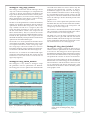
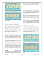
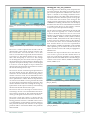
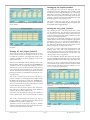
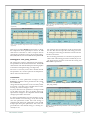
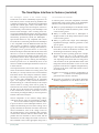
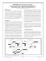
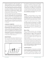
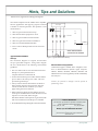
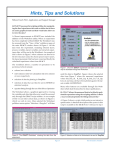
TCAD Driven CAD
A Journal for Circuit Simulation and SPICE Modeling Engineers
Local Optimization Templates for Extracting
BSIM3v3.1 Parameters in UTMOST III
Introduction
The BSIM3v3.1 SPICE model has become an industry
standard for modeling deep-submicron MOS technologies.
The model is suitable for both digital and analog applications because of the better modeling of the output
conductances and the physics based scaling which is
embedded in the model equations. The model offers
binning parameters for improving the model fits for
certain devices. The BSIM3v3.1 model has been implemented in UTMOST III and SmartSpice since its first
introduction.
The UTMOST user group has continuous interest in
creating better BSIM3v3.1 models for their customers.
This article is written to provide the latest local optimization templates perfected in Silvaco’s model characterization lab.
Data Collection and Initial
Parameter Extraction
The final quality of the optimized model depends
heavily on the quality of collected data and the initial parameter extraction. UTMOST has a powerful
automatic BSIM3v3.1 parameter extraction algorithm
which is a part of the “BSIM3_MG” routine. The data for
BSIM3v3.1 modeling should always be collected by using the BSIM3_MG routine. (See articles for BSIM3_MG
extraction routine in the previous issues of the Simulation Standard.) The UTMOST extraction manual volume
#1 also covers the entire operation of the BSIM_MG
routine.
The recommended number of points per sweep in the
BSIM3_MG routine is 51 and the number of VGS steps
and VBS steps are 5. The Voffset value which is used to
calculate the the first VGstart value for the ID/VD characteristics (Vgstart = VTextracted + Voffset) defaults to
0.5V. The Voffset value may seem high for some analog
users who like to see the data closer to the threshold
voltage. However the RDS related parameters are extracted better if the Voffset is around 0.5V. The user
should pay attention to the measured characteristics of
each device to make sure that there are no problem devices in the device array which is used for modeling.
Volume 9, Number 1, January 1998
The typical number of geometries used for model parameter extraction is 10 to 12. There should be a large
device with wide W and long L (to avoid short channel
or narrow width effects) to extract the root parameters
(threshold voltage, mobility, etc.). The wide W and
shortest L device and array of common wide W and
short L devices should be present in the test chip to extract short channel effects. The long L and narrowest W
device and maybe one or two more narrow W and long
L devices should be present in the test chip to extract the
narrow width effects. The last critical device geometries
which need to be in the test chip are the small devices.
The small devices are the narrow W and short L devices.
The shortest L and narrowest W and one or two more
small devices should be used for modeling. These are
the devices which require many of the binning parameters within the BSIM3v3.1 model.
Local Optimization Strategies
After the data is collected the initial set of parameters is
extracted by the BSIM3_MG routine. The ALL_DC routine can be used for local optimization. In this article’s
example a single ALL_DC routine will be used. The different types of data will be displayed in the ALL_DC
graphics screen for different optimization strategies.
This may require more user interface but it is easier to
follow each step of local optimizations this way. Later
the user may automate the local optimization strategies by utilizing the different ALL_DC routines. The
operation of the local optimization is explained in the
UTMOST user manual.
Continued on page 2....
INSIDE
The SmartSpice Interface to Cadence (revisited) ...................7
CellRATER from Taveren Technology ..................................8
Cell Characterization with .MODIF Statement
in SmartSpice ..................................................................10
Calendar of Events ..............................................................13
Hints, Tips, and Solutions ..................................................14
SILVACO
INTERNATIONAL
Strategy #1: idvg_large_bsim3v3
and width offset effects for narrow devices only. The
strategy#2 will optimize the “Current” of “ID/VG”
characteristics (Figure 4). The narrow W and long L
devices should be selected for each row in this strategy.
It is recommended to select typically 2 narrow W and
long L devices. The ID/VG characteristics of the selected
narrow W and long L devices should be present in the
graphics screen.
This strategy is used for the wide W and long L device
only. As it can be seen in the figure 1, it will optimize the
“Current” of “ID/VG” characteristics. The Wide W and
long L device should be selected in the “Geometry Selection Screen” (figure 3.) for each row in this strategy. The
ID/VG characteristics of this device ( wide W and long
L) should be present in the graphics screen.
The first row is used to optimize the parameters for the
threshold shift (K3, W0) and the width offset (WINT).
There is no back bias effect so the “sweep/start” and
“sweep/stop” are set to 1 (Figure 5).
The first row of the optimization is used for the threshold,
mobility and mobility degradation related parameter
optimization. Therefore the “sweep/start” and “sweep/
stop” variables are both set to 1 (Figure 2) This will
ensure that these parameters in row#1 will only use
the data with VBS=0V (which is the sweep#1 for the
ID/VG characteristics). The %5 to %100 for the current
range will guarantee that the subthreshold data will not
be used for this optimization. This is logical since the
threshold and mobility related parameters should not be
optimized for the subthreshold region.
The second row includes the back bias effects (K3B) but
only concentrates around the threshold region. Therefore the current max is set to 40% (Figure 5).
The third row is for the final re-optimization of the
width offset and its gate field and back bias effects
(DWG and DWB). The threshold region is not included
for this optimization therefore the current min is set to
25% and current max is set to 100% (Figure 5).
The second row is used to optimize the back bias effects
on threshold and mobility. The difference in the second
row compare to the first row is the “sweep/stop” value.
The “sweep/stop” value in the second row is set to 5 to
include the remaining sweeps in the ID/VG characteristics which have the VBS value other than 0. (Figure 2).
Strategy #3: idvg_short_bsim3v3
The strategy#3 is similar to strategy#1 and #2. The geometries used for optimization are wide W and short
L for each row. The strategy#3 is used to optimize the
threshold shift and length offset and channel resistance
effects for the short channel devices only. The strategy#3
will optimize the “Current” of “ID/VG” characteristics
The third row is created for the subthreshold region
parameters NFACTOR and VOFF. The current min and
current max is set to 1E-10 to 1E-7 to cover the sub VT
region only. (Figure 2.)
(Figure 6). The wide W and short L devices should be selected for each row in this strategy. It is recommended to
select maximum 3 wide W and short L devices for each
row of optimization. The ID/VG characteristics of the
selected wide W and short L devices should be present
in the graphics screen.
Strategy #2: idvg_narrow_bsim3v3
The strategy#2 is very similar to strategy#1 except
the geometries used for optimization are different.
The strategy#2 is used to optimize the threshold shift
Figure 1. Local optimization strategy definition screen for Strategy#1
(idvg_large_bsim3v3)
Figure 2. Local optimization target selection screen for Strategy#1
(idvg_large_bsim3v3)
The Simulation Standard
Figure 3. Local optimization geometry selection screen for Strategy#1 (idvg_large_
bsim3v3)
Page 2
January 1998
initial values and minimum and maximum limits for
the local optimization. It is suitable to select 2 or 3 small
devices for each row of optimization. The ID/VG characteristics of the selected narrow W and short L devices
should be present in the graphics screen.
The first row is used to optimize the parameters for
the threshold shift (PVTH0) and the channel resistance
(PRDSW) adjustment for small devices. There is no back
bias effect so the “sweep/start” and “sweep/stop” are
set to 1 (Figure 9). If there is a need to adjust the mobility or the mobility degradation parameters for the small
devices, the binning parameters (PU0, PUA or PUB can
be added to row#1).
Figure 4. Local optimization strategy definition screen for Strategy#2
(idvg_narrow_bsim3v3)
The second row includes the back bias effects (PK2) but
only concentrates around the threshold region. Therefore the current max is set to 40% (Figure 9). This parameter is optional. If the back gate effects are modeled
well with existing model after running the strategy#1,
#2 and #3 then there is no need to include the parameter
“PK2” in the optimization. The same logic applies for all
binning parameters. The user should check the fits after
strategy #1, #2 and #3 and then make a judgment call
based on the fits for the small device to run strategy#4
with default settings or to add or to subtract some of the
binning parameters.
Figure 5. Local optimization target selection screen for Strategy#2
(idvg_narrow_bsim3v3)
The first row is used to optimize the parameters for the
threshold shift (DVT0, DVT1, NLX), length offset (LINT) and
channel resistance (RDSW). There is no back bias effect so the
“sweep/start” and “sweep/stop” are set to 1 (Figure 7).
The second row includes the back bias effects (DVT2)
but only concentrates around the threshold region.
Therefore the current max is set to 40% (Figure 7).
Strategy #5: idvd_0vb_bsim3v3
The first 4 strategies concentrated only on the linear
regions (ID/VG) of different geometries. The strategy#5
will use the ID/VD data (saturation region) for optimization (Figure 10). Strategy#5 also uses different geometries for each row of the local optimization. The ID/VD
at VB=0V characteristics of the all optimized devices
should be present in the graphics screen.
The third row is for the final re-optimization of the
width offset and its gate field and back bias effects
(PRWG and PRWB). The threshold region is not included for this optimization so the current min is set to 20%
and current max is set to 100% (Figure 7).
Strategy #4: idvg_small_bsim3v3
The strategy #4 is in the same family of optimization
strategies as Strategy#1, #2 and #3. The geometries
used for optimization should be narrow W and short L
devices only. Strategy #4 will optimize the “Current” of
“ID/VG” characteristics (Figure 8). The difference in this
strategy compared to #1,#2 and #3 is the parameters.
The original BSIM3v3.1 model does not have a variety
of parameters for modeling the small device effects.
The threshold voltage adjustment parameters such as
DVT0W, DVT1W and DVT2W are not recommended for
use in small geometry effect modeling. Therefore the
binning parameters should be utilized for the regions
where there is a need for model improvement. Usually
the threshold voltage and high gate field effects in the
linear region need some improvement. The binning parameters PVTH0 and PRDSW parameters are included
in strategy#4 to compensate the lack of standard model
parameters for modeling the small device effects. The
binning parameters are not included in the original
UTMOST parameter table for the BSIM3v3.1 model.
Therefore if there is a need to utilize these parameters
they should be added to the parameter table with some
January 1998
Figure 6. Local optimization strategy definition screen for Strategy#3 (idvg_short_
bsim3v3)
Figure 7. Local optimization target selection screen for Strategy#3 (idvg_short_
bsim3v3)
Page 3
The Simulation Standard
Strategy #6: rds_0vb_bsim3v3
The strategy#6 has few different points compared to the
rest of the strategies. The strategy#6 is used for the output resistance optimization. Therefore the “Derivative”
option is selected in the Strategy Definition Screen”
(Figure 12). The log scale “RDS/VDS” characteristics for
all optimized devices should be present in the graphics screen before the execution of the strategy#6. The
output resistance optimization is the most difficult part
of BSIM3v3.1 modeling. Therefore the user should pay
attention to the measured vs simulated data and include
or exclude certain devices in the geometry selection
screen to improve the optimization strategy.
Figure 8. Local optimization strategy definition screen for Strategy#4 (idvg_small_
bsim3v3).
For the output resistance optimization the wide W and
long L device and typically 2 or 3 wide W and short
L devices should be selected in row#1. In row#1 total
number of 11 parameters are selected for optimization:
“PCLM, PDIBLC1, PDIBLC2, PVAG, DROUT, DELTA,
PSCBE1, PSCBE2, ETA0, DSUB” If the wide W and long
L device seem to be dominant factor for the optimization results, this device can be excluded and only the
short channel devices can used for re-optimization.
The parameters “PSCBE1 and PSCBE2” can be excluded
when optimizing for the PMOS devices because the
impact ionization current will usually be negligible for
PMOS devices.
Figure 9. Local optimization target selection screen for Strategy#4 (idvg_small_
bsim3v3).
The row#1 is used to optimize the ID/VD at VB=0V
characteristics of the wide W and long L device only.
The “Current Min.” and “Current Max” is set to 1E-6
and 1 to cover the entire range of ID/VD characteristics
1µA (Figure 11). The default settings for the “Sweep/
Start” and “Sweep/Stop” is set to 3 to 5. This settings
can be changed by the user based on the fits quality. If
the model needs more improvement for the higher VGS
steps then Sweep Start and Stop values can be changed
to 4 and 5 to cover the higher VG steps of the ID/VD
characteristics. The parameters A0 and AGS are used for
the wide W and long L device only.
The row#2 is used for saturation region optimization of
the short channel devices only. Therefore the wide W
and short L devices should be selected in the geometry
selection screen for row#2. It is recommended to select
maximum of 3 devices (typically 2). The default parameter for optimization is “VSAT”. However the parameters
A1 and A2 can be added to row#2 given that the model
can not be improved with the existing parameters. This
decision should be made after running the strategy #6
(optimization of the output resistances) and examining
the fits for the ID/VD characteristics again.
Sometimes the output resistance fits for the small devices are not as good as the short channel devices. In
such cases some binning parameters can be added to
improve the fits for the small devices. These binning parameters can be such as: PETA0, PPDIBLC1, PPDIBLC2,
PPVAG, PDROUT, etc.
Figure 10. Local optimization strategy definition screen for Strategy#5
(idvd_0vb_bsim3v3).
The row#3 is same as row#2 except it is used for narrow
W and long L devices. It is recommended to select maximum 3 devices (typically 2). The parameters B0 and B1
usually provide good fit results for narrow W devices.
The row#4 is used only if there is a need for the improvement of small device ID/VD characteristics. The
binning parameter “PVSAT” is included in the row#4 as
a recommendation for the binning parameter selection.
This parameter (PVSAT) does not exist in the original
parameter table so it should be added to the parameter
table if needed.
The Simulation Standard
Figure 11. Local optimization target selection screen for Strategy#5
(idvd_0vb_bsim3v3).
Page 4
January 1998
Strategy #8: rds_highvb_bsim3v3
The strategy#8 is very similar to strategy#6. The only
difference is that the “RDS/VDS” data which is used
for optimization has high VBS (Figure 16). For the high
VBS output resistance optimization the wide W and
short L devices (typically two) should be selected in the
geometry selection screen and the selected device data
should be present in the graphics screen.
The row#1 is the only active row in strategy#8. The
parameters “ETAB and PDIBLCB” should be optimized
for the RDS/VDS at high VBS data.
Figure 12. Local optimization strategy definition screen for Strategy#6
(rds_0vb_bsim3v3).
Strategy #9: idvg_temp_bsim3v3
Up to strategy#9 only room temperature data is used
for the optimizations. The Strategy#9 and strategy#10
are used for the optimization of the temperature parameters. Therefore the data which is different to room
temperature should be loaded to UTMOST before running strategy#9 and #10. The strategy#9 is used for the
optimization of the threshold and mobility adjustment
parameters. Each row is used for the optimization of
the different geometries. The ID/VG characteristics at
low VDS (0.1V) should be present in the graphics screen
before running the strategy#9 (Figure 18).
Figure 13. Local optimization target selection screen for Strategy#6 (rds_
0vb_bsim3v3).
The row#1 is used to adjust the threshold (KT1) and
mobility (UTE, UA1, UB1) with temperature for the
wide W and long L device only. The back bias effects are
not included in row#1 therefore the “Sweep/start” and
“Sweep/stop” is set to 1 (Figure 19).
Strategy #7: idvd_highvb_bsim3v3
The strategy#7 is used for the high VBS ID/VD characteristics of all devices. In strategy#7 each row is used
for different geometries. The high VBS ID/VD characteristics should be present in graphics screen for all
optimized devices.
The row#2 includes the back bias effects into the optimization (added parameters KT2 and UC1). The selected
geometry should be wide W and long L only. (Figure 19).
The row#3 is used to optimize the temperature effects
on threshold (KT1L) and the channel resistance (PRT)
for the wide W and short L devices. Typically two devices are selected for optimization.
The row#1 is used for the wide W and long L device only.
The parameter “KETA” is the only standard BSIM3v3.1
parameter used for the high VBS modeling of ID/VD
characteristics. However this parameter usually doesn’t
scale well for the short channel, narrow width and small
devices. Therefore in the following row#2 #3 and #4 the
binning parameters are introduced to provide the scaling. (Figure 14).
The row#2 is used for narrow W devices only. The parameter “WKETA” is a binning parameter and it should
be added to the parameter screen by the UTMOST user.
Typically 2 narrow W and long L devices are suitable for
the row#2 optimization. The row#2 should be activated
only the fit improvement is needed.
Figure 14. Local optimization strategy definition screen for Strategy#7 (rds_
0vb_bsim3v3).
The row#3 is used for short L devices only. The parameter “LKETA” is a binning parameter and it should be
added to the parameter screen by the UTMOST user.
Typically 2 wide W and short L devices are suitable for
row#2 optimization. The row#3 should be activated
only fit improvement is needed.
The row#4 is used for narrow W devices only. The parameter “PKETA” is a binning parameter and it should
be added to the parameter screen by the UTMOST user.
Typically 2 narrow W and short L devices are suitable
for the row#2 optimization. The row#4 should be activated only fit improvement is needed.
January 1998
Figure 15. Local optimization target selection screen for Strategy#7 (rds_0vb_
bsim3v3).
Page 5
The Simulation Standard
Figure 16. Local optimization strategy definition screen for Strategy#8 (rds_highvb_bsim3v3).
Figure 18. Local optimization strategy definition screen for Strategy#9 (idvg_
temp_bsim3v3).
Figure 19. Local optimization target selection screen for Strategy#9 (idvg_temp_
bsim3v3).
Figure 17. Local optimization target selection screen for Strategy#8 (rds_highvb_bsim3v3).
There are no standard BSIM3v3.1 parameters to adjust
the temperature effect specifically for narrow W and
small devices. Therefore in order to improve the fits
some binning parameters such as: WUTE, PUTE, WKT1,
PKT1, PPRT, WUA1, PUA1 can be added to the optimization.
Some strategies may provide better results if executed more
than once. The user can repeat the same strategy few times.
The strategy#5 and strategy#6 should be executed one after
another several times.
The less binning parameters are used the more physical the
model will be. The binning parameters should only be used
if the improvement cannot be made with the existing standard BSIM3v3 parameters.
Strategy #10: idvd_temp_bsim3v3
The strategy#10 is used for optimization of the temperature parameters for the ID/VD characteristics. The ID/VD
characteristics at 0V VBS should be present in the graphics
screen before running the strategy #10 (Figure 20).
The row#1 is used only for the short channel devices.
The parameter AT is used to optimize the temperature
effects on ID/VD characteristics.
Conclusion
A total of 10 local optimization strategies for the
BSIM3v3.1 model have been presented in this article.
The UTMOST user should go into each strategy and
change the selected geometries in the “Geometry Selection Screen” according to the available devices before
running any of these strategies. Some UTMOST users
may have different local optimization strategies based
on the older setup files. They can modify their local
optimization strategies to be compatible with the latest
strategies presented in this article.
It is NOT recommended to run all 10 strategies at once.
The user should run each strategy one by one and observe the optimization results after each strategy is
completed. The main local optimization screen should
be kept open during the optimization. This screen is a
good indicator if the selected strategy is running successfully or not.
The Simulation Standard
Figure 20. Local optimization strategy definition screen for Strategy#10
(idvd_temp_bsim3v3).
Figure 21. Local optimization target selection screen for Strategy#10 (idvd_
temp_bsim3v3).
Page 6
January 1998
The SmartSpice Interface to Cadence (revisited)
The SmartSpice interface to the Cadence Design
Framework II has been substantially improved in its
latest release (version 1.0.8.R), following feedback from
a number of existing users. The interface is implemented
through the Cadence Spice Socket, and enables users
of Cadence’s Analog Artist and Composer software to
interact directly, and seamlessly, with SmartSpice. The
interface works through a series of Analog Artist control screens implemented by Silvaco using the Cadence
OASIS interface. Because it depends on the sophisticated
functionality provided by OASIS, the SmartSpice /
Spice Socket interface is only compatible with version
4.4.0 (and above) of the Design Framework. SmartSpice
is also compatible with the HSPICE Socket built into
older versions of Cadence’s Composer, Edge and Artist products, although access through this interface to
SmartSpice’s more powerful features is necessarily
limited. The improvements described in this article take
the form of a series of enhancements (including some
bug fixes) which have been made to several of the existing interface features. These improvements are part of
an on-going project aimed at making the SmartSpice
interface provide access to substantially more of the
features available in SmartSpice itself than was the case
in earlier releases.
also annotated to the schematic.
In summary, then, a brief, but complete list of features
implemented in the current release of the SmartSpice
interface to the Cadence Design Framework II is:
One important feature, fixed in this release, is the generation of hierarchical netlists from Analog Artist, and
the ability to correctly annotate sub-circuit simulation
information back to the Composer schematic window.
The ability to annotate operating points and currents
has also been fully implemented for all component
types. An example of a fully annotated subcircuit is
illustrated in Figure 1. The functionality of the analysis
control screens in Analog Artist will be greatly enhanced in the next release of the SmartSpice interface;
the first step in this direction has already been taken
in the current release, however, in the form of a set of
control items providing the ability to save bias points in
both DC and transient analyses.
Several components of the Cadence design library
‘analogLib’ did not allow the instantiation of SmartSpice views on the Cadence Composer schematic editor
in previous releases of the SmartSpice interface; an example is the file-based, piece-wise linear voltage source
(vpwlf). This behavior has been corrected in the current
release. Furthermore, none of the voltage sources in
the analogLib library were annotating their operating
currents to the schematic editor in the last release. This
problem has been rectified in version 1.0.8.R, and the
characteristics of both voltage and current sources have
been extended so that, where appropriate, the power is
January 1998
●
Ability to specify SmartSpice as the default simulator in the Setup->Simulator/Directory/Host control
screen of Analog Artist.
●
Ability to include model files in SmartSpice or
cdsSpice format in the Setup->Environment control
screen of Analog Artist.
●
Ability to generate PSF output from SmartSpice,
implemented through automatic generation of the
“psf=2” option.
●
Annotation of node voltages to the Composer schematic editor, selected via the Results->Annotate-> DC
Node Voltages menu item in Analog Artist.
●
Annotation of device operating points (for example,
device currents, gds, etc.) to the Composer schematic
editor, selected via the Results->Annotate>DC Operating Points menu item in Analog Artist,
and controlled via the opPointLabelSet field of the
Interpreted Labels Information section of the CDF
properties in the Silvaco-supplied analogLib library,
accessed via the Tools->CDF->Edit control screen in
the Cadence CIW.
●
●
Support for marching waveforms, implemented via
the SmartSpice waveform viewer through automatic
generation of the “.IPLOT” statement.
Direct plot of waveforms in the Cadence Waveform
Window, implemented via the Results->Direct Plot
Continued on page 11....
Figure 1. An example of subcircuit back annotation.
Page 7
The Simulation Standard
CellRATER from Taveren Technology –
Fast, Accurate Cell Library Characterization for
Deep Submicron Timing Flow Improvement
John Croix and Jerry Gebhard, Tavern Technology
Introduction
Generally speaking, cell-based timers are faster because
they deal with less data. One would expect transistorbased static timers to be more accurate due to the finer
granularity of the analysis. In practice this isn’t always
true, and the tradeoffs for this finer granularity are CPU
time and limits on the amount of data that can be
successfully analyzed. CellRATER was developed in an
attempt to give the end user the best of both worlds. Improved accuracy for the cell-based user, and improved
throughput for the transistor-based user. (For those
users whose tools can run in mixed-mode, cells and
transistors at the same time, substituting CellRATER
data for standard cells improves the throughput, while
maintaining the accuracy)
Taveren Technology, Inc., a startup company based in
Austin, Texas is busy developing the next generation
performance characterization tool suite. CellRATER, a
cell library characterization tool, is the first product in
this suite. It is up to 10 times faster and 10 times more accurate than the competition. This article will attempt to
give you an understanding of how CellRATER achieves
these goals using Silvaco’s SmartSpice, and the benefits
that can be gained in the overall timing design flow.
Background
Over the past few years, static timing analysis has
become an acceptable signoff method for high speed
digital designs. Generally, static timing tools fall into
2 categories: cell-based static timers, typically used by
ASIC designers, and transistor-based static timers, more
commonly used by custom IC designers. Both methods suffer from a lack of accuracy when compared to
SmartSpice, but the improvement in analysis time is
usually what convinces users the tradeoff is necessary.
Both types of timing tools rely on pre-characterized data
for the primitive elements in the analysis. Cell-based
tools rely on a library of characterization data, typically
made up of standard or gate array cells. Transistor-based
tools rely on tables of data for various transistor sizes.
An additional and equally important benefit to the
cell-based user is the positive impact these improved
libraries have on synthesis. It is generally accepted
knowledge in the industry that problems caused by
synthesis are really the fault of poorly developed and
characterized libraries.
Traditional Approach
To understand our method of characterization, it is
helpful to review the traditional approach. In its most
basic form, cell characterization is the process of applying
a voltage stimulus to an input pin, placing a capacitive
load (Cload) on an output pin, and measuring the
propagation delay (td) through the cell and rise/fall
times (tout) on the output pin.
The deficiencies of both types of static timers are well
known. First and foremost is the fact that they are only
as accurate as the characterization data they rely on.
Input Stimulus
Output Response
C load
C in
t out
t in
td
Figure 1. Traditional approach to cell characterization.
The Simulation Standard
Page 8
January 1998
Recently this approach was taken a step farther. Attempts to improve the accuracy of cell models led to
the development of the non-linear table model. The nonlinear table model increases accuracy by allowing the
effects of input edge transition time (tin) on the propagation delay (td) and output rise/fall times (tout) to be taken
into account. Unfortunately, it still lacks a place-holder
for information on variations of Cin with respect to Cload
and tin that we can provide. (These variations impact
the previous driving stage rise/fall times, and should be
included in future versions of the model.)
this constraint, we apply innovative error-minimizing
techniques to reduce the oversampled data to either a
lookup table or set of equation coefficients suitable for
use in synthesis, static timing analysis or event-driven
simulation tools. For example, if the measured data
consisted of 400 points, data reduction could reduce this
to 36 points (6x6 table). When this table is used to predict
the response of the cell, it would yield typical results within
0.5% of SmartSpice over the entire range of measurement (not just the measured points).
Typical characterization tools measure the response of a
cell at a small number of points that are chosen manually
by the user. This limited data set is used to populate the
table model, which in turn is used to predict the overall
response of the cell. By using interpolation between
the points or fitting it to a fixed-form equation, new
response values are chosen during static timing analysis or synthesis. Our research has shown that these
interpolation errors can typically be on the order of
15 -50% of what the true response would be if measured
in SmartSpice.
Speed
In addition to offering the highest accuracy available,
CellRATER offers impressive efficiency. While it might
seem that more CPU resources would be required by our
oversampling approach, we have demonstrated that by
taking advantage of SPICE setup features, it actually
takes less time to complete the characterization process.
In addition, for those who have access to multiple,
networked computers, the performance of our system
scales almost linearly with the number of computers.
Our system uses a client-server architecture to take
full advantage of your SmartSpice licenses. Because we
have a custom interface, the use of SmartSpice as the
SPICE engine in our system ensures the most optimum
solution for speed.
CellRATERʼs Approach
As contrasted to the above approach, CellRATER can produce a 6x6 lookup table for a combinational or sequential
(flip-flop) cell that predicts response to within 0.5% (typical) of SmartSpice, after interpolation by Synopsys. That
accuracy is typical across the entire range of response,
not just at the measured points. CellRATER uses a unique
method of oversampling and data reduction that guarantees more reliable and more accurate results than traditional methods. Yet speed is not compromised. In fact,
even though we sample at many more points than other
commercially available packages, our runtimes are less. In
fact, they can be as much as 10 times less.
Ease-of-Use
There is a beneficial side-effect to the oversampling
technique. Users do not have to pick their own sampling
points. The process is entirely automatic. Ease-of-use
doesn’t stop there. We supply a set of standard cell
templates encoded in our proprietary SpicePILOT language. With our templates, most standard cells can be
set up for characterization within a few minutes with
little or no changes.
Data Reduction
Because we collect more data than traditional tools, we
have a much better representation of the true response
of the cell. However, we are still constrained with producing a “reduced table” of this data (for synthesis and
static timing run-time performance reasons). To handle
Traditional characterization often involves many steps
repeated across hundreds of cells resulting in hundreds,
if not thousands, of simulation runs which have to be
post-processed, organized, and manually tracked by the
user. CellRATER offers a pushbutton system that allows
you to manage the entire process reliably for thousands
of cells. It tracks SmartSpice jobs seamlessly across any
number of distributed computer systems.
Response
Time
Data Management
Capacitive Load
Another powerful feature of the system is its centralized
data storage for both the raw characterization data and the
results. An application programming interface (API) allows you to access this data for any purpose – reports,
cross-checks, regression analysis, charting, etc. This
means you don’t have to rerun jobs to retrieve the raw data.
Td2
Input
Transition
Time
Td3
C2
C3
Figure 2. Table model approach to modeling response as a
function of Capacitance Load and Input Transition Time.
January 1998
Page 9
The Simulation Standard
External Formats
change or cell design iteration, otherwise additional errors will be introduced into the library data. We pick the
characterization points automatically, which means we
have accurate data for every change. But as an added
benefit, CellRATER includes an integrated analysis
module that generates error reports allowing the user to
verify the accuracy of the entire library.
CellRATER can generate a variety of EDA vendor formats.
However, it is easy to generate your own formats by using
the data management API to access raw data or results.
Reliability
Characterization is a complex, tedious process involving hundreds or thousands of simulations, potentially across multiple computers. This process must be
tracked for consistency and accuracy otherwise errors
could be introduced into the flow. For example, a failed
simulation job on a given system could prevent a cell
from completing normally. With our system, the tedious
bookkeeping involved in tracking the characterization
of a library is handled automatically and reliably. In the
event of an error or job failure due to a power or network outage, our checkpoint feature allows the user to
easily restart a characterization from the point of failure.
As path delays descend into the sub-nanosecond
range, the statistical likelihood of input pins switching
simultaneously increases. In datapath logic, simultaneous
switching is a virtual certainty. Traditional methods
ignore the effects of simultaneous switching, introducing
inaccuracies of 20% or more into propagation delays,
Cin calculations and output rise/fall times. CellRATER
offers an optional module that allows the effect of simultaneously switching inputs to be considered.
Benefits to Your Design Flow
Using cell library characterization data built with
CellRATER and SmartSpice, cell-based static timing
analysis now becomes much more reliable in predicting
overall timing performance. Our studies have shown
that static timing results on paths of 10-12 levels of logic
came within 2% of SPICE for the same circuit. The benefit to you and your design team is timing reports you
can believe, the elimination of wasted design time, and
higher quality products. Not a bad investment.
Other Features
It is important to know the accuracy of your libraries.
Without the ability to automatically generate error reports, cell libraries suffer gradual degradation in quality
as they progress through design iterations and process
changes. With traditional tools, the user must manually
pick the new characterization points with each process
...continued from page 7
menu in Analog Artist, combined with user selection
in the Composer schematic editor.
●
Hierarchical netlisting capability, implemented
through SmartSpice/Spice Socket name mapping
routines in the OASIS interface.
●
New Silvaco-supplied versions of the Cadence basic
and analogLib libraries, incorporating SmartSpice
views of all appropriate devices.
●
Compatibility with ac, dc, transient and noise analyses,
via the Choosing Analyses control screen in Analog
Artist.
●
●
LDIF, LIMPTS, LIST, LOGIC, METHOD, NODE, NOMOD, NOPAGE, NUMDGT, OPTS, PIVREL, PIVTOL,
RAWPTS, RELTOL, SCALE, SCALM, SRCSTEPS,
TEMP, TNOM, TRTOL, TRYTOCOMPACT, TTICK,
VNTOL, VSTA, VZERO, WIDTH
The main aspect of the next release will be a complete
rewrite of the SmartSpice analysis control screens in
Analog Artist, adding support for more specialized
SmartSpice functionality, including:
Ability to save bias points in dc and transient analyses,
via the Choosing Analysis control screen in Analog
Artist.
Ability to configure the following SmartSpice options from within the Simulator Options control
screen in Analog Artist:
ABSTOL, ACCT, ACCURATE, ACM, AUTOSTOP,
BYPASS, CAPDC, CAPMOD, CAPTAB, CHGTOL,
COEF1, CONV, DCGMCHK, DCGMIN, DCGMSTEPS,
DCIAP, DCPATH, DEFAD, DEFAS, DEFL, DEFPD,
DEFPS, DEFNRD, DEFNRS, DEFW, DISTRIBUTION,
EXPERT, FORMAT, GMIN, GMINSTEPS, HDIF, ICG,
INTEGR, INTERP, ITL1, ITL2, ITL4, ITL41, ITL5, LD,
The Simulation Standard
Page 10
●
Support for the “CallV”/”SaveV” and “UIC” options
in AC and DC analyses.
●
Support for the “TRANOP” calculation of operating
point option.
●
Support for the specification of a maximum internal
step in transient analysis.
●
Support for the specification of the options “RAWPTS”,
“INTERP”, etc. in transient analysis.
●
Support for nested sweeps of device, parameter, or
temperature in AC and DC analyses.
●
Support for the specification of maximum iterations,
tolerances, etc. in DC analysis.
January 1998
Cell Characterization with .MODIF Statement in SmartSpice
Introduction
SmartSpice provides many unique and powerful
features to facilitate parametric analysis in general and
cell characterization in particular. As discussed in [1],
a typical use of these features is in the generation of
lookup tables for timing tools, such as those provided
by Synopsys. These tables relate propogation and delay
times to variations in parameters such as input transition times and load capacitance values. The features
of SmartSpice that are most applicable to this form of
analysis are the .MODIF and .MEASURE statements.
Another form of characterization that is particularly
important is the computation of setup and hold time for
sequential circuits. These calculations are more difficult
than standard parameter sweeps and require some additional features of the .MODIF statement and of the
SmartSpice command processor, to maximize the
efficiency of these simulations. This article will focus on
the efficient use of the .MODIF statement when applied
to the problem of cell characterization.
.MODIF Statement
The .MODIF statement is the most flexible and powerful
statement for parametric analysis and optimization in
SmartSpice. In its most simple form it allows the user
to simultaneously modify any number of parameters in
the input file. Parameters that can be modified include
device parameters, model parameters, parameter labels
(.PARAM) and temperature. Parameter variations can be
expressed as constant increments (+= and -=) or multipliers (*= and /=) of an initial value, lists of possible values
or statistical distributions.
The .MODIF statement can have multiple sets of parameter variation, with each set being separated using the
MODIF keyword. An example of a .MODIF statement
with two sets is shown in Example 1.
.MODIF LOOP = 5
+ temp = 100
+ cload(cap) = 1.2p
+ rise_time += (0.5n) 0.1n
+ MODIF LOOP = 5
+ cload(cap) = list( 0.5p 0.7p 1.0p 1.2p 1.5p )
Example 1: .MODIF statement with multiple simulation sets.
In this example 5 simulations will first be run with temperature and load capacitance held constant, and ‘rise_
time’ swept from 0.5ns in increments of 0.1ns. Once the 5
simulations are completed the next set will be executed.
Parameters will retain the final value from the previous
set of simulations, unless the new set explicitly changes
the value. For example, during the second set of simulations, the temperature will be 100oC and ‘rise_time’ will
be 0.9ns. The value of the load capacitance will be swept
using the supplied list of values. Hence, a total of 10
simulations will be executed.
January 1998
Clock
Input
Tin
Time
Tck
Figure 1. Typical approach taken to determine setup time.
In the previous example each MODIF set executes a
fixed number of simulations, i.e. the stop criteria for
the loop is specified using the LOOP keyword. For any
MODIF set, it is possible to also specify a conditional
stop criteria as a function of a particular measurement
in the circuit. This is particularly useful if a circuit
will succeed for some initial values of parameter, but
eventually fail to behave correctly for a particular parameter value. Since the value at which this will occur
is unknown to the user, use of a conditional stop can
significantly reduce simulation time by stopping simulation after the first failure, and ignoring the remaining
redundant simulations. An example of a .MODIF analysis with a conditional stop is given in Example 2.
.MODIF LOOP = 20 STOP del_rise LE 1.1n
+ rise_time = 0.5ns
+ cload(cap) += (0.1pF) 0.2pF
Example 2: .MODIF statement with conditional stop.
In this example ‘del_rise’ is a measurement performed
after a simulation. A maximum of twenty simulations
(LOOP = 20) will be performed, with the load capacitance
swept from 0.1pF in increments of 0.2pF. SmartSpice
will interrupt this MODIF set once twenty simulations
have been performed OR the value of the ‘del_rise’ measurement is less that or equal to 1.1ns. The conditional
stop is set by the “STOP del_rise LE 1.1n” portion of the
statement.
Once simulation of a particular MODIF set is interrupted,
SmartSpice will move to the next set if it exists or move
to the next stage of simulation. Each MODIF set can
contain both absolute and conditional stop criteria. By
combining conditional stops with multiple MODIF sets,
it is possible to create a very efficient method of characterizing setup/hold time.
Setup and Hold Time Computation
The setup time of a circuit is defined as the minimum
time prior to some event, usually a clock edge, that an
input to the circuit must remain stable to ensure reliable
device operation. The hold time is defined as the time
that the input must remain stable after the event.
Page 11
The Simulation Standard
The typical approach taken to characterize the setup
time is shown is Figure 1. A clock edge is generated at
the time Tck, and the input node changes value at the
time Tin. Initially Tin is such that the output of the cell
performs as expected. Then Tin is incremented by the
required resolution of the eventual solution until a stop
value is reached. The setup time is then taken as the Tck
- Tin for the last valid simulation.
In this example, up to 31 simulation could be performed,
however only one simulation that fails will be performed.
Hence, if the setup time is 1ns, ~10 simulation can be
skipped. This can result is significant time savings, especially if the AUTOSTOP option is being used to halt
simulation once all measurements are complete. Simulations that fail will simulate up to the final time, i.e. 20ns,
while simulations that succeed will typically only need
to be simulated up to ~12n (depending on propogation
delay and output rise time).
In an input deck, this can be achieved in a number of
different ways. Example 3(b) shows the use of a nested
transient sweep and Example 3(c) shows the use of a
.MODIF analysis. Example 3(a) shows the definition of
the input and clock pulses, with the measurement of the
maximum output voltage and the difference between
the edge of both pulses.
Binary Search Method
The problem of calculation of the setup/hold time of a
circuit is similar to the problem of searching for an element in an already sorted set. A binary search is much
faster and consequently more efficient than a standard
linear search. This technique can also be applied to the
search for a setup/hold time and can be accomplished
through use of multiple MODIF sets and conditional
stops. This technique is illustrated in Example 5.
.PARAM tck=10n tin=7n
Vck ck 0 pulse 0.0 3.3 ‘tck’ 1n 1n 100n
Vd
d
0 pulse 0.0 3.3 ‘tin’ 1n 1n 100n
.MEASURE max_q MAX v(q)
.MODIF LOOP=4 STOP max_q LE 1.6
.MEASURE setup TRIG v(d) RISE=1 VAL=1.6
+
TARG v(ck) RISE=1 VAL=1.6
+ tin += (7n) 1n
.MEASURE tpd
TRIG v(d) RISE=1 VAL=1.6
+
TARG v(q) RISE=1 VAL=1.6
+ tin -= 0.5n
+MODIF LOOP=2 STOP 1.6 LE max_q
+MODIF LOOP=2 STOP max_q LE 1.6
(a)
+ tin += 0.25n
+MODIF LOOP=3 STOP 1.6 LE max_q
.TRAN 0.01n 20n SWEEP tin 7n 10n 0.1n
+ tin -= 0.1n
(b)
Example 5: Binary search of setup time using .MODIF.
.TRAN 0.01n 20n
In this example, ‘tin’ is initially incremented in 1ns steps
until the circuit fails. When this happens the second
MODIF set will decrement ‘tin’ in 0.5ns intervals until
the output voltage is again greater than 1.6V. At this
stage the setup time has been calculated to a accuracy
of 0.5ns. To get to the required resolution of 0.1ns, two
more MODIF sets are used, with steps in ‘tin’ of 0.25ns
and 0.1ns respectively.
.MODIF LOOP=31
+ tin += (7n) 0.1n
(c)
Example 3: a) Portion of input netlist, b) Nested
transient sweep, c) .MODIF implementation of nested
transient sweep in b).
As can be seen in this example, 31 simulations will be
required to compute the setup time to a resolution of
0.1ns. Depending upon the cell being characterized, this
approach can result in many of the simulations failing.
For example if the setup time is 1ns, then all simulations
with ‘tin’ > 9ns will fail.
This approach results in a calculation of the setup time
to the required accuracy in a worst case of 8 simulations,
as compared to the original 31 simulations. To increase
the resolution by a factor of 2, only 1 more simulation is
needed, whereas with the linear search, 31 more simulations
are needed.
To increase the efficiency of the characterization, it is
possible to use a conditional stop to prevent unnecessary
simulations taking place. Typically the cell is taken to
fail if the output voltage fails to pass a certain threshold
value. If the maximum or minimum value of the output
voltage is measured, this can be used in the stop condition, as
shown in Example 4.
Conclusion
This article has discussed the use of the .MODIF statement in the characterization of cells. This statement can
greatly increase the efficiency of characterization by
reducing the number of simulations required and
performing all characterization stages within one process. In a future article, some more advanced uses of the
MODIF statement in combination with the SmartSpice
command interpreter will be discussed.
.MODIF LOOP=31 STOP max_q LE 1.6
+ tin += (7n) 0.1n
Example 4: Use of .MODIF to reduce number of simulations.
The Simulation Standard
Page 12
January 1998
Calendar of Events
January
1
2
3
4
5
6
7
8
9
10
11
12
13
14
15
16
17
18
19
20
21
22
23 W/S - Yokohama, Japan
24
25
26
27
28
29
30
31
February
1
2
3
4
5
6
7
8
9
10
11 W/S - Scottsdale, AZ
12 W/S - Scottsdale, AZ
13
14
15
16
17
18
19
20 W/S - Yokohama, Japan
21
22
23
24
25
26
27
28
Bulletin Board
Production Ramp-up for
S3245A Noise Amplifier!
Due to strong demand and customer acceptance,
Silvaco has increased production volume in
Q1 1998 for its S3245A Noise Amplifier. This
combined with powerful noise measurement and
parameter extraction routines in UTMOST III,
has established Silvaco as the industry leader in
measuring and modeling flicker noise in MOS
devices.
European SPICE Model
Development Group!
To better support our growing European
SmartSpice customer base, Silvaco has
established a development group with a focus
on developing and supporting SPICE model
originating from Europe. Based in Grenoble, this
group will collaborate with the leading model
development centers. Immediate priorities will
be Philips Level 9, EKV for MOS and Philips
MEXTRAM for Bipolar technologies.
See Silvaco at San Francisco DAC!
Silvaco will be exhibiting the latest in TCAD
Driven CAD tools at the Design Automation
Conference. The exhibition will be 15-17th June
at the Moscone Center, San Francisco. Silvaco
will present the latest advances in:
●SmartSpice
●NT-based Layout and Verification Tools
●Technology based Parasitic Extraction
●3D TCAD
For more information on any of our workshops, please check our web site at http://www.silvaco.com
The Simulation Standard, circulation 17,000 Vol. 9, No. 1, January 1998 is copyrighted by Silvaco International. If you, or someone you know wants a subscription to
this free publication, please call (408) 567-1000 (USA), (44) (1483) 401-800 (UK), (81)(45) 820-3000 (Japan), or your nearest Silvaco distributor.
Simulation Standard, TCAD Driven CAD, Virtual Wafer Fab, Analog Alliance, Legacy, ATHENA, ATLAS, MERCURY, VICTORY, VYPER, ANALOG EXPRESS,
RESILIENCE, DISCOVERY, CELEBRITY, Manufacturing Tools, Automation Tools, Interactive Tools, TonyPlot, TonyPlot3D, DeckBuild, DevEdit, DevEdit3D,
Interpreter, ATHENA Interpreter, ATLAS Interpreter, Circuit Optimizer, MaskViews, PSTATS, SSuprem3, SSuprem4, Elite, Optolith, Flash, Silicides, MC Depo/Etch,
MC Implant, S-Pisces, Blaze/Blaze3D, Device3D, TFT2D/3D, Ferro, SiGe, SiC, Laser, VCSELS, Quantum2D/3D, Luminous2D/3D, Giga2D/3D, MixedMode2D/
3D, FastBlaze, FastLargeSignal, FastMixedMode, FastGiga, FastNoise, Mocasim, Spirit, Beacon, Frontier, Clarity, Zenith, Vision, Radiant, TwinSim, , UTMOST,
UTMOST II, UTMOST III, UTMOST IV, PROMOST, SPAYN, UTMOST IV Measure, UTMOST IV Fit, UTMOST IV Spice Modeling, SmartStats, SDDL, SmartSpice,
FastSpice, Twister, Blast, MixSim, SmartLib, TestChip, Promost-Rel, RelStats, RelLib, Harm, Ranger, Ranger3D Nomad, QUEST, EXACT, CLEVER, STELLAR,
HIPEX-net, HIPEX-r, HIPEX-c, HIPEX-rc, HIPEX-crc, EM, Power, IR, SI, Timing, SN, Clock, Scholar, Expert, Savage, Scout, Dragon, Maverick, Guardian, Envoy,
LISA, ExpertViews and SFLM are trademarks of Silvaco International.
January 1998
Page 13
The Simulation Standard
Hints, Tips and Solutions
Mustafa Taner, Applications and Support Engineer
Since the first shipment of the S3245A Noise Amplifier,
Silvaco’s applications and support group has collected
a number of customer questions. The questions can be
summarized as:
1. What is typical measurement set-up?
DC Analyzer
S3245A NOISE AMPLIFIER
POWER
2. What measurement equipment is used?
DC ANALYZER
3. What is typical method of measurement?
VD
4. What are typical measurement conditions?
VG
VS
VB
DUT
DSA
DSA
5. What is recommended SPICE model?
OUT
6. How to extract SPICE parameters from measured
result?
Noise Measurement
Connection for S3245A
Typical Measurement
Set-Up
Figure 1. Typical Measurement Set-Up.
The connection diagram for atypical measurement
set-up is presented in Figure 1. Along with a diagram
the user should observe the following measurement
guidelines:
•
Measurement Equipment
UTMOST III supports S3245A Noise Amplifier and a
host of Hewlett-Packard dynamic signal analyzers:
HP3561, HP3562, HP35660, HP35665, HP35670 and
HP3589. DC bias can be supplied by all HP and Keithley
DC analyzers.
The coax cables used for noise measurement should
be kept away from potential noise sources such as
computer monitors or instrument displays.
• Connect all instrument power cables and the S3245A
power cable to the same power outlet. This will
prevent the ground loops.
Answers for questions 3 through 6 will be printed in
forthcoming issues.
• Always measure the DC characteristics of the DUT
before starting the noise measurements. Note the
current level for the bias conditions you want to
apply during noise measurements.
• When connecting the DUT to the S3245A, first turn
on the power of S3245A then connect the device in the
sequence of source, bulk, drain and gate.
• Disconnect the DUT in the sequence of gate, drain, bulk
and source and then turn off the power of S3245A.
Call for Questions
• Do not disturb the setup during the noise measurements.
If you have hints, tips, solutions or questions to contribute, please
contact our Applications and Support Department
Phone: (408) 567-1000
Fax: (408) 496-6080
e-mail: [email protected]
Hints, Tips and Solutions Archive
Check our our Web Page to see more details of this example
plus an archive of previous Hints, Tips, and Solutions
www.silvaco.com
The Simulation Standard
Page 14
January 1998
Join the Winning Team!
Standardize your process/device
and CAD design using Silvaco’s
“TCAD Driven CAD™”
To get a demo and product description contact or visit a Silvaco office near you:
• Santa Clara
• Phoenix
• Austin
• Boston
• Guildford
• Grenoble
• Munich
SILVACO
INTE R N AT I O N A L
USA HEADQUARTERS
Silvaco International
4701 Patrick Henry Drive
Building 2
Santa Clara, CA 95054
USA
Phone:
Fax:
408-567-1000
408-496-6080
[email protected]
www.silvaco.com
• Tokyo
• Seoul
• Hsinchu
CONTACTS:
Silvaco Japan
[email protected]
Silvaco Korea
[email protected]
Silvaco Taiwan
[email protected]
Silvaco Singapore
[email protected]
Silvaco UK
[email protected]
Silvaco France
[email protected]
Silvaco Germany
[email protected]
Products Licensed through Silvaco or e*ECAD
Ve n d o r P a r t n e r