1
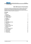
PCI-1149.1
Boundary-Scan Controller
Features
•
Half-Slot IEEE-1149.1
Boundary Scan (JTAG)
compatible PCI card.
•
32 bit PCI bus interface,
buffered with two FIFOs to
support high data transfer
rates.
•
Supports four independent
JTAG ports. One port can
be configured as differential or single-ended
•
JTAG ports and parallel I/O
are programmable from 2.0
to 3.4V and are 5V
compatible
•
User programmable test
clocks (TCK) with speeds
up to 25 MHz
•
Internal or external scan
test clock source
•
16 inputs and 16 outputs of
programmable parallel I/O
•
External freeze input to
asynchronously enable or
disable the TCK
•
•
•
Scan Function Library
software for Windows
95/NT
Plug and play Windows
95/NT device drivers
Built-in self-test features
Overview
Block Diagram
The PCI-1149.1 is a sophisticated test
controller that can be used in the
testing of devices, boards, or systems
compliant with the IEEE-1149.1
standard. Using 2 Parallel/Serial
converter devices, this PCI bus tester
supports up to four independent
Boundary-Scan chains. 16 parallel
inputs and 16 parallel outputs including
two open collector drivers are provided
to test or control non-boundary-scan
logic of the unit under test. Software
controlled voltage translating logic
allows the PCI-1149.1 to be used to
test low-voltage systems.
The PCI-1149.1 contains several
performance enhancing functional
sections aimed at increasing test vector
throughput. A functional block diagram
of the PCI-1149.1 is shown in Figure 1.
A set of software drivers written in C is
supplied with the tester card to allow
the end user to create powerful test
programs that are tailored to his or her
needs.
Key functional elements are the dual
Test Access Port (TAP) controllers that
are fed by two FIFOs, one for receive
data and one for transmit data.
This provides a high data rate to and
from the PCI bus, regardless of actual
test clock speeds. All functions of the
PCI-1149.1 are controlled by a state
machine that contains status and
control registers that can be accessed
through the PCI bus.
Programmable Clocks
The PCI-1149.1 TCK outputs to the
IEEE Standard 1149.1 compatible
Connector
Connector
JTAG Connector
Port A
8 Parallel Outputs
Port B
8 Parallel Outputs
Port B
8 Parallel Inputs
Port B
8 Parallel Inputs
Target Presence
Detection Capabilies
JTAG Bus 1
JTAG Bus 2
TAP
Controller
•
FIFO
JTAG Bus 3
JTAG Bus 4
TAP
Controller
FIFO
•
Control/
Status
Registers
Progmble
Clock
Generator
PCI Interface
RS-422
Figure 1. PCI-1149.1 Block Diagram
target system are programmable under
software control. A wide range of TCK
frequencies can be achieved by using
the on-board TCK generation circuitry.
The user is given the ability to select
one of three on-board oscillators from
which to base the TCK output. The user
can then modify this frequency using
the on-board divider circuitry to select
the desired frequency. Should it
become necessary to use a TCK
frequency other than one that can be
supplied by the on-board circuitry, the
user is given the option of generating
the TCK outputs to the target system
from an externally supplied clock or
replacing one of the on-board
oscillators. The maximum clock speed
is 25 MHz. In order to compensate for
cable and circuit time delays however,
the maximum clock rate needs to be
reduced to 15-20 MHz.
Adjustable Low
Voltage Outputs
The voltage level of the parallel I/O and
the 4 TAP interfaces is software
programmable and can be set to any
voltage between 2.0V and 3.4V in
increments of 0.05V. These interfaces
are 5V compatible and 5V tolerant at
all programmed levels.
differential signals on one of its four
TAPS. The RS-422 option is selected
under software control by writing to the
appropriate register. This allows the
boundary-scan tester to be located at
a greater distance from the unit under
test than would otherwise be possible.
Parallel Input/Output
Ports
The PCI-1149.1 contains 16 parallel
inputs and 16 parallel outputs. The
input and output signals are organized
into two 8 bit parallel ports. The parallel
input and output ports are accessible
from the host computer by reading or
writing the appropriate register. The 16
parallel outputs are driven by D-latches
and the outputs can be put into a high
impedance state by writing to a register.
The input and output ports can be used
to control and sense various functions
in the target system which cannot be
controlled or observed through
boundary-scan operations. These
ports are useful for testing of target
systems that incorporate components
that are not compliant to IEEE Standard
1149.1.
As an alternative to using one of the
ports, two open collector outputs are
available and are controlled by writing
to a register. Open collector signals
are often needed to drive reset and
emulation signals.
Differential Inputs/
Outputs
The PCI-1149.1 has the ability to drive
and receive RS-422 compatible
The PCI-1149.1 has a pin (T_OFF*) on
the JTAG interface connector that can
be used to detect the presence of the
target board. The state of the T_OFF*
signal can be monitored by reading bit
0 of Input Port A. When using this
feature, the T_OFF* signal should be
connected through a pull-up to target
power, so when power is on, a logic
high will be sensed on this signal. This
pin has no other effect on the operation
of the board.
Built-in Self-Test
The PCI-1149.1 has a built-in self-test
capability. Logic has been provided at
the JTAG connector to read back,
synchronously with TCK, data shifted
out on TMS and TDO for each of the
TAPs. Similarly, logic has been
provided to drive each of the TDIs at
the TAP interface. In this way the TAPs
can be fully tested
PCI Bus Interface
The PCI-1149.1 is a single-slot, single
fucntion 5V/32 bit 33 MHz PCI device
completely compliant with Revision 2.1
of the PCI Bus Specification.
Scan Function "C"
Library
Software drivers (Scan Function
Library) and a self-test program are
provided with the PCI-1149.1 card. The
software is coded in ‘C’ and is provided
as a 32 bit DLL for Windows NT or
Windows 95. The software drivers
provide the user with the functions that
are necessary to operate the JTAG
ports and to send JTAG instructions
and data to the target system. The user
can incorporate the drivers in his own
application software and only code the
higher level test procedures.
The self-test software sends JTAG
instruction and data words to the onboard Boundary-scanned ICs. This
code is the actual ‘C’ language code
for the executable program TEST.EXE
included on the disk.
The Scan Function Librar y (SFL)
provided can be classified into two
categories:
•
Scanning
•
Utility/Low-level access
The Scanning functions provide a
higher level access to the operation of
the PCI-1149.1 Board.
The table below lists all the SFL
routines:
circulate_dr()
This function starts by flushing out data
from selected target’s Data Register
(DR) by scanning in the selected bit
length + 16 zeros. Then the function
will scan the flushed out data back into
the target’s DR.
hard_reset()
This function will perform a hard reset
of all the board’s functions. The TCK
generators are set to their lowest
speed, the TAP controllers are reset
and their outputs enabled, the FIFOs
are reset, TRST* is pulsed low then
high for all TAPs, the parallel outputs
are enabled, the TMS is reset, and the
self-test features are disabled. RS-422
is selected or not selected and the
voltage level of the JTAG and I/O
interfaces is set.
move_to_state()
Transitions the target JTAG device’s
state machine to the desired final stable
state.
read_io()
This function reads the input from the
selected 8-bit input port.
scan_dr()
Scans data, from a specified array, out
the PCI-1149.1 card and into the target
JTAG device’s Data Register (DR).
Data that is scanned out of the target
JTAG device’s Data Register (DR) into
the PCI-1149.1 card during the
operation is stored in a specified array.
The first bit scanned out is the LSB of
the output array’s first member. The first
bit scanned in is stored in the LSB of
the input array’s first member. Following
the scan operation, the device’s JTAG
state machine is left in the Run-Test/
Idle state.
scan_dr_turbo()
Scans data, from a specified array, out
the PCI-1149.1 card into the target
JTAG device’s Data Register (DR)
using hardware acceleration. Most
effective for data arrays larger than 512
bytes. Data that is scanned out of the
target JTAG device’s Data Register
(DR) into the PCI-1149.1 card during
the operation is stored in a specified
array. The first bit scanned out is the
LSB of the output array’s first member.
The first bit scanned in is stored in the
LSB of the input array’s first member.
Following the scan operation, the
device’s JTAG state machine is left in
the Run-Test/Idle state.
scan_ir()
Scans data, from a specified array, out
the PCI-1149.1 card into the target
JTAG device’s Instruction Register (IR).
Data that is scanned out of the target
JTAG device’s Instruction Register (IR)
into the PCI-1149.1 card during the
operation is stored in a specified array.
The first bit scanned out is the LSB of
the output array’s first member. The first
bit scanned in is stored in the LSB of
the input array’s first member. Following
the scan operation, the device’s JTAG
state machine is left in the Run-Test/
Idle state.
scan_ir_turbo()
Scans data, from a specified array, out
the PCI-1149.1 card into the target
JTAG device’s Instruction Register (IR)
using hardware acceleration. Most
effective for data arrays larger than 512
bytes. Data that is scanned out of the
target JTAG device’s Instr uction
Register (IR) into the PCI-1149.1 card
during the operation is stored in a
specified array. The first bit scanned out
is the LSB of the output array’s first
member. The first bit scanned in is
stored in the LSB of the input array’s
first member. Following the scan
operation, the device’s JTAG state
machine is left in the Run-Test/Idle
state.
scan_NxCLK()
Scan clocks through the interface
without toggling TMS or TDO.
scan_to_pause_dr()
Scans data, from a specified array, out
the PCI-1149.1 card into the target
JTAG device’s Data Register (DR).
Data that is scanned out of the target
JTAG device’s Data Register (DR) into
the PCI-1149.1 card during the
operation is stored in a specified array.
The first bit scanned out is the LSB of
the output array’s first member. The first
bit scanned in is stored in the LSB of
the input array’s first member. Following
the scan operation, the device’s JTAG
state machine is left in the Pause-DR
state.
scan_to_pause_ir()
Scans data, from a specified array, out
the PCI-1149.1 card into the target
JTAG device’s Instruction Register (IR).
Data that is scanned out of the target
JTAG device’s Instruction Register (IR)
into the PCI-1149.1 card during the
operation is stored in a specified array.
The first bit scanned out is the LSB of
the output array’s first member. The first
bit scanned in is stored in the LSB of
the input array’s first member. Following
the scan operation, the device’s JTAG
state machine is left in the Pause-IR
state.
set_scan_clk()
This function will set the TCK clock
speed for the specified TAP pair. Note
that the TCK is only present during
tms_reset(), move_to_state() and scan
operations.
set_io()
This function sets the output levels of
the selected 8-bit output port. The
programmable voltage levels are set by
the hard_reset() function.
set_oc_output()
This function sets the open collector
output level, of the selected bit, on
output port A.
test()
This function is a simple test of the
application program’s ability to execute
library function calls. It simply returns
the integer you passed in when called
correctly.
tms_reset()
Hold TMS signal high for 5 TCKS to
put device’s JTAG state machine into
Test-Logic Reset state.
trst_reset()
Pulse the TRST* signal low then high
on the selected TAP to reset those
JTAG devices that support the TRST*
signal. Places the TAP in Test-Logic
Reset state.
I/O Connectors
Input Port Connector (P1) 34 pin IDC
Compatible with SCANPLUS™
Family of Products
The PCI-1149.1 is both hardware and software compatible
with the complete SCANPLUS™ family of IEEE-1149.1 and
IEEE-P1149.5 test products. Consequently, test programs
developed for other Corelis tester platforms will run on the
PCI-1149.1 and vice-versa.
8/16/32 bit
Interrupts
INTA# (optional)
4
Maximum TCK frequency:
25 MHz
Parallel and TAP DC Characteristics
User’s Programmable I/O Voltage (Vcc)
= 2.7-3.4V
MAX
UNIT
2.0
3.4
V
2.0
V
V
= 2.7-3.4V
0.8
V
= 2.7V
-12
mA
= 3.0V
-24
mA
= 2.7V
12
mA
24
mA
CC
High Level Output Current
I
V
MIN
CC
IL
OH
V
CC
V
CC
I Low Level Output Current
OL
(3M part no. 2534-6002UB or equivalent)
JTAG Connector (P3)
40 pin IDC
Operating Environment
Temperature:
0°C to 55°C
IEEE-1149.1
Number of TAP Controllers:
V Low Level Input Voltage
34 pin IDC
Power Requirements
(From host expansion bus)
5V @1.5A maximum
PCI Interface
Bus Width
IH
Output Port Connector
(3M part no. 3432-5203 or equivalent)
Specifications
V High Level Input Voltage
(3M part no. 2534-6002UB or equivalent)
V
Relative Humidity:
10% to 90%, non-condensing
Storage Environment
Temperature:
-40°C to 85°C
Relative Humidity:
0% to 100%, non-condensing
Supplied With the Module
•
PCI-1149.1 Boundary-Scan Controller Card
•
Scan Function Library and self-test software disk
•
User’s Manual.
CC
V
= 3.0 V
CC
V
OH
I
= -100mA
OH
V
=2.0-3.4V
CC
(Hi-level
I = -12mA
Output Voltage) OH
V -0.2
V
CC
V = 2.7V
2.2
V
2.4
V
2.2
V
CC
V = 3.0V
CC
I
= -24mA
OH
V
OL
I
V = 3.0V
CC
= 100mA
OL
I = 12 mA
(Low-level
OL
Output Voltage)
I = 24 mA
OL
V
= 2.0-3.4V
0.2
V
0.4
V
0.55
V
CC
V =2.7V
CC
V = 3.0V
CC
Physical
Board Outline Dimensions (PCB):
3.8" x 5.5" (PCI short card)
Windows® and WindowsNT® are trademarks of Microsoft
Inc.
ScanPlus™ is a trademark of Corelis Inc.
© Copyright 1998 by Corelis Inc. All rights reserved.
Permission granted to make copies for free distribution.
12607 Hiddencreek Way
Cerritos, California 90703
Tel: (562) 926-6727, Fax: (562) 404-6196
[email protected]
http://www.corelis.com
CORELIS INC., reserves the right to make changes in design or
specification at any time without notice.