1
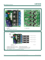
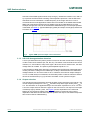
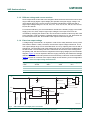
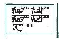
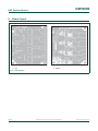
UM10689 SSL2109ADB1121 4-channel DC-to-DC LED driver demo board Rev. 1.1 — 13 May 2013 User manual Document information Info Content Keywords SSL2109T, SSL2109AT, SSL2109ADB1121, buck, controller, reference board, LED driver, PWM Abstract This document explains the operation and application of the SSL2109AT 4-channel, small form factor demo board. The demo board incorporates four independent DC-to-DC switch mode current drivers with a common input power stage. By default, the board is optimized to drive 1 A (typical) per channel. The board is particularly suitable for use in street and high-bay lighting applications. Multiple user configuration options are available for the demo board; some options require components changes. UM10689 NXP Semiconductors SSL2109ADB1121 4-channel DC-to-DC LED driver demo board Revision history Rev Date Description v.1.1 20130513 Section 3.1.6 and Section 4.3 added; Table 3 reformatted v.1 20130326 first issue Contact information For more information, please visit: http://www.nxp.com For sales office addresses, please send an email to: [email protected] UM10689 User manual All information provided in this document is subject to legal disclaimers. Rev. 1.1 — 13 May 2013 © NXP B.V. 2013. All rights reserved. 2 of 16 UM10689 NXP Semiconductors SSL2109ADB1121 4-channel DC-to-DC LED driver demo board 1. Introduction WARNING Lethal voltage and fire ignition hazard The non-insulated high voltages that are present when operating this product, constitute a risk of electric shock, personal injury, death and/or ignition of fire. This product is intended for evaluation purposes only. It shall be operated in a designated test area by personnel qualified according to local requirements and labor laws to work with non-insulated mains voltages and high-voltage circuits. This product shall never be operated unattended. The SSL2109AT 4-channel demo board demonstrates the LED driving capabilities of the SSL2109AT device. The SSL2109T (with Short-Winding Protection (SWP)) could replace the SSL2109AT on the demo board if SWP is required. Typical target applications for the demo board include LED street lighting, high and low bay lighting, and refrigeration lighting. Each channel is individually dimmable using Pulse Width Modulation (PWM). The circuit contains four Boundary Conduction Mode (BCM) buck converters and a common input power stage. The BCM buck converter is a true switch-mode current source. Key features of the board include: • • • • • Up to 98 % efficiency • • • • • Low-cost LED driver solution User-configurable output current (no custom-made magnetic components needed) Intrinsically protected against short-circuit, open load and overtemperature conditions BCM buck converters operate as true switch-mode current sources Operates with input voltages ranging from 33 V (DC) to 600 V (DC) with some component changes Small form factor PWM dimming Independent or combined channel control No LED binning required Applications: • Street lighting • High and low bay lighting • Refrigeration lighting Figure 1 is a populated view of the demo board; Figure 2 shows the connections. UM10689 User manual All information provided in this document is subject to legal disclaimers. Rev. 1.1 — 13 May 2013 © NXP B.V. 2013. All rights reserved. 3 of 16 UM10689 NXP Semiconductors SSL2109ADB1121 4-channel DC-to-DC LED driver demo board aaa-006920 aaa-006921 a. top view Fig 1. b. bottom view SSL2109ADB1121 demo board PWM input Ch1 and Ch2 Optional Auxiliary supply 48-52 V GND (5) (3) (6) - (1) (4) + (2) Ch1: 4-12 LEDs 13-43 V @ 1A + Ch2: 4-12 LEDs 13-43 V @ 1A + Ch3: 4-12 LEDs 13-43 V @ 1A + Ch4: 4-12 LEDs 13-43 V @ 1A (6) (5) PWM input Ch3 and Ch4 aaa-006922 (1) Main DC supply input (48 V to 52 V) (3) Optional auxiliary supply (15 V to 20 V) (5) PWM inputs (Ch1 to Ch4) Fig 2. (2) Main supply ground (GND) (4) Jumper for internal/external VCC supply (6) LED string connections (Ch1 to Ch4) SSL2109ADB1121 demo board showing connections UM10689 User manual All information provided in this document is subject to legal disclaimers. Rev. 1.1 — 13 May 2013 © NXP B.V. 2013. All rights reserved. 4 of 16 UM10689 NXP Semiconductors SSL2109ADB1121 4-channel DC-to-DC LED driver demo board 2. Specifications Table 1. Demo board specifications Parameter Value Comment Output current 1A the channels can be configured individually Supply voltage 48 V (DC) to 52 V (DC) the board can be used with other combinations of input/output voltages; it is recommended to keep the switching frequency between 20 kHz and 200 kHz Output voltage 13 V to 43 V at 52 V (DC) input voltage Efficiency > 90 % see Figure 5 Auxiliary supply voltage 15 V (DC) to 20 V (DC) optional Switching frequency 65 kHz to 120 kHz at 52 V (DC) input voltage PWM frequency 0.1 kHz to 1 kHz dimming resolution < 1 % Board dimensions 51 mm 58.5 mm length width 3. Functional description 3.1 Introduction The SSL2109AT multi-channel demo board circuit consists of a general power input section and four SSL2109AT current source sections. Each of the current source sections contains the following blocks: common power input, dimming input, switching circuit, current measurement/feedback and output. Figure 9 is a circuit diagram of the demo board default configuration. The BOM component list is detailed in Table 3. 3.1.1 General power input section The common power input section of the default demo board consists of a buffer capacitor (C18) and terminal TB5. TB5 has two ports and must be connected to the mains input DC voltage (48 V to 52 V) and to ground, as marked on the board. J4 can be connected to an auxiliary power supply (15 V (DC) to 20 V (DC)). By default, jumper J1 (a 2-way female jumper) connects the VCC supply voltage to the SSL2109ATs via resistors R12, R13, R14 and R15. So the auxiliary supply is not needed in the default configuration. 3.1.2 PWM dimming sections The PWM dimming input signals are connected to the IC input ports via J2 and J3, as indicated on the PCB (see Figure 2). 10 nF capacitors are used for low-pass filtering. Voltage reference D9 is provided for fast booting of the SSL2109AT ICs. Alternatively, C13, C14, C15 and C16 can be tied to ground. The dimming input signals are connected to the SSL2109AT control pins (NTC). When a low voltage signal (0.4 V < Vlow < 0.3 V) is supplied to this pin, the SSL2109AT converter is effectively disabled. A high voltage (0.53 V < Vhigh < 5.2 V) on the same pin causes the SSL2109AT to be fully enabled. The light output can be varied by toggling between low and high voltages on pin NTC. Typically, the light output is exactly proportional to the duty ratio of the PWM dimming signal. In principle, any PWM frequency is acceptable for PWM dimming. In practice, a very low PWM frequency can give the impression that the LED string is flickering. A very high frequency can result in inaccurate dimming, since PWM dimming resolution is proportional to the ratio between the switching frequency and PWM frequency. The UM10689 User manual All information provided in this document is subject to legal disclaimers. Rev. 1.1 — 13 May 2013 © NXP B.V. 2013. All rights reserved. 5 of 16 UM10689 NXP Semiconductors SSL2109ADB1121 4-channel DC-to-DC LED driver demo board slew-rate of the PWM signal must be steep enough (> 2200V/sec between 0.2 V and 0.3 V) to prevent the SSL2109AT activating overtemperature protection. See the SSL2109 data sheet for more information. A PWM frequency in the range 100 Hz to 1 kHz is recommended for most applications. SMD coils are mounted on the default demo board. SMD coils generate the least amount of audible noise when PWM dimming is used. Cheaper through-hole coils can be substituted if PWM dimming is not used (as specified in the BOM, see Table 3). Typical PWM input (yellow) and output current (pink) waveforms are shown in Figure 3. aaa-006802 Fig 3. Typical PWM input and output current waveforms 3.1.3 SSL2109 demagnetization detection A new cycle starts when the primary switch is turned on and the current starts to ramp up via the current sense resistors (R1, R2, R3, R4). The switch is turned off when the current reaches Ipeak, and it starts to ramp down again. When the current reaches zero, the drain voltage starts to oscillate. The peak-to-peak amplitude equals 2 × VO. A special feature called valley detection is integrated into the SSL2109. Dedicated built-in circuitry senses the voltage on the DRAIN pin. A valley is detected when the differential voltage between VHV and VDRAIN falls to 25 V. Therefore, the minimum output voltage is 12.5 V. If a valid valley is not detected, the secondary stroke continues until the maximum off-time of the SSL2109 (toff(high)) has been exceeded. A new cycle then begins. 3.1.4 Output selection The switching section generates a sawtooth-shaped current waveform in the inductor. The current ramps up linearly from 0 A to Ipeak and then ramps down again linearly from Ipeak to 0 A. This waveform is not applied directly to the LED load. Capacitors C9, C10, C11 and C12 in the output sections reduce the ripple on the LED current. The output current ripple is relatively high by default (<30%, see Figure 3) and is dependent on the LED load. Ripple can be reduced by adding extra output capacitance, although higher output capacitance will affect the transient response speed at the output. The transient response time must be fast for PWM dimming. UM10689 User manual All information provided in this document is subject to legal disclaimers. Rev. 1.1 — 13 May 2013 © NXP B.V. 2013. All rights reserved. 6 of 16 UM10689 NXP Semiconductors SSL2109ADB1121 4-channel DC-to-DC LED driver demo board 3.1.5 Different voltage and current versions Some components would need to be changed to allow the demo board to be used to drive longer LED strings (higher output voltage) and operate at a higher supply voltage. The input voltage rating of the circuit can be increased by substituting components with a higher input voltage rating for C18, C9, C10, C11, C12, C5, C6, C7, C8, Q1, Q2, Q3, Q4, D5, D6, D7 and D8. For maximum efficiency, it is recommended to use either the auxiliary supply or the DVDT supply (C23, C24, C25, C26) for higher input voltages. The output current can be controlled by changing the values of R1, R2, R3 and R4. Inductance value may also need to be changed in order to maintain a suitable switching frequency. D1, D2, D3 and D4 can be used instead of D5, D6, D7 and D8 if lower output currents are required. 3.1.6 Extra low output voltage A voltage swing of at least 25 V is required in order for the valley detection circuitry of the SSL2109A to detect a valley. Therefore, the minimum output voltage is limited to 12.5 V. The output voltage range can be extended below 12.5 V by replacing the buck coil with a transformer. The secondary side of the transformer can be connected to the DRAIN pin on the SSL2109A. The secondary side of the transformer should have more windings than the primary side; this will increase the magnitude of the ringing voltage (see the schematic diagram, Figure 4). R16 is required to filter the ringing caused by the transformer leakage inductance. The converter still operates as a true boundary conduction mode buck SMPS. Table 2 provides an overview of the output voltage versus efficiency for this configuration. Table 2. Extra low output voltage measurements PI (W) VI (V) IO (mA) VO (V) efficiency (%) 4.668 48.505 986.7 3.833 81.0 7.689 48.480 970.9 6.839 86.4 10.554 48.457 952.7 9.835 88.8 13.373 48.435 938.1 12.834 90.0 TB2 Vin 1 C5 1 μF 100 V C9 2.2 μF 63 V D1 PMEG6030EP 4 6 1 3 U2 HV VCC VCC NTC PWM1 SOURCE 8 1 2 3 4 SSL2109A 7 6 5 R16 DRAIN 100 kΩ GND DVDT D10 PMEG6030EP DRIVER LED+ 2 LED- OSTTC020162 T1 N(4,6):N(1,3)=1:5 Vin 4 2 Q1 PHT6NQ10T 1 3 C13 10 nF 50 V R5 220 kΩ C1 1 μF 50 V R1 0.25 Ω aaa-007475 Fig 4. SSL2109A extra low output power schematic UM10689 User manual All information provided in this document is subject to legal disclaimers. Rev. 1.1 — 13 May 2013 © NXP B.V. 2013. All rights reserved. 7 of 16 UM10689 NXP Semiconductors SSL2109ADB1121 4-channel DC-to-DC LED driver demo board 4. Performance data 4.1 Efficiency The SSL2109AT 4-channel demo board is suitable for driving long or short LED strings. High efficiency figures (98 %) are normally only obtained with relatively long LED strings. Figure 5 gives an indication of the level of efficiency that can be expected from the demo board. Efficiency levels are consistent over a wide range of output voltages. aaa-006803 100 % 90 80 70 60 50 40 30 20 10 0 Fig 5. UM10689 User manual 10 20 30 40 Vout 50 Efficiency curve All information provided in this document is subject to legal disclaimers. Rev. 1.1 — 13 May 2013 © NXP B.V. 2013. All rights reserved. 8 of 16 UM10689 NXP Semiconductors SSL2109ADB1121 4-channel DC-to-DC LED driver demo board 4.2 Load and Line regulation The output current of the SSL2109AT 4-channel demo board varies slightly with the load and the supply voltage. The curves in Figure 5 and Figure 6 demonstrate that the demo board has excellent load and line regulation properties, which is ideal for general lighting purposes (line regulation was measured by changing the critical default capacitors to similar types with higher voltage ratings). The slight variations in light output intensity are barely visible to the human eye. aaa-006805 1100 LED current (A) 900 700 500 300 100 Fig 6. 10 20 30 40 Vout 50 Load regulation aaa-006806 1100 LED current (A) 900 700 500 300 100 Fig 7. UM10689 User manual 40 50 60 70 Vin 80 Line regulation All information provided in this document is subject to legal disclaimers. Rev. 1.1 — 13 May 2013 © NXP B.V. 2013. All rights reserved. 9 of 16 UM10689 NXP Semiconductors SSL2109ADB1121 4-channel DC-to-DC LED driver demo board 4.3 Output current accuracy One hundred SSL2109ADB1121 demo boards were constructed, each containing four SSL2109AT current source sections. The current at the output of all four hundred LED string drivers was measured under typical conditions. Figure 8 shows how the measurement results were distributed. aaa-007474 250 number of measurments 200 150 100 50 0 Fig 8. 0.93 0.94 0.95 0.96 0.97 0.98 0.99 VO (A) 1.00 Distribution chart of VO measurements for all 400 LED drivers 5. ElectroMagnetic Interference (EMI) The SSL2109AT 4-channel demo board is pre-compliant with EMC regulations. UM10689 User manual All information provided in this document is subject to legal disclaimers. Rev. 1.1 — 13 May 2013 © NXP B.V. 2013. All rights reserved. 10 of 16 xxxxxxxxxxxxxxxxxxxxx xxxxxxxxxxxxxxxxxxxxxxxxxx xxxxxxx x x x xxxxxxxxxxxxxxxxxxxxxxxxxxxxxx xxxxxxxxxxxxxxxxxxx xx xx xxxxx xxxxxxxxxxxxxxxxxxxxxxxxxxx xxxxxxxxxxxxxxxxxxx xxxxxx xxxxxxxxxxxxxxxxxxxxxxxxxxxxxxxxxxx xxxxxxxxxxxx x x xxxxxxxxxxxxxxxxxxxxx xxxxxxxxxxxxxxxxxxxxxxxxxxxxxx xxxxx xxxxxxxxxxxxxxxxxxxxxxxxxxxxxxxxxxxxxxxxxxxxxxxxxx xxxxxxxx xxxxxxxxxxxxxxxxxxxxxxxxx xxxxxxxxxxxxxxxxxxxx xxx Vin D1 PMEG6030EP n.m. D5 V8P10-M3/86A L1 VDD U1 5V HV C13 10 nF 50 V VCC NTC PWM1 SOURCE 1 2 7 3 6 4 5 DRAIN C23 100 nF 100 V 2 4 n.m. GND DVDT 1 DRIVER 1 C19 3.3 μF 100 V n.m. C9 2.2 μF 63 V 47 μH 8 2 LED- OSTTCC020162 L11 n.m. D6 V8P10-M3/86A L2 HV VCC NTC SOURCE C2 1 μF 50 V R6 220 kΩ 47 μH 1 8 2 7 3 6 4 5 DRAIN C24 100 nF 100 V 2 4 n.m. GND DVDT 1 DRIVER SOURCE 2 2 VinR12 13 kΩ OSTTC020152 R13 13 kΩ R14 13 kΩ R15 13 kΩ C18 330 μF 63 V B28 2 5V 1 3 PWM2 4 5 CES-150-01-S-S J4 R11 2 Vaux- 180 Ω VCC R10 4.7 kΩ CES-150-01-S-S 5V D9 BZX84-C5V1 C17 100 nF 50 V LED- OSTTCC020162 L13 n.m. Q3 PHT6NQ10T 3 D4 PMEG6030EP n.m. D8 V8P10-M3/86A L4 NTC C4 1 μF 50 V 47 μH 1 8 2 7 3 6 4 5 SSL2109AT DRAIN GND DVDT DRIVER C26 100 nF 100 V 2 4 n.m. 1 C12 2.2 μF 63 V C22 3.3 μF 100 V n.m. 1 2 LED+ LED- OSTTCC020162 47 μH L14 n.m. Q4 PHT6NQ10T 3 R4 0.25 Ω 1 2 PWM4 PWM3 5V 3 4 5 CES-150-01-S-S aaa-006807 UM10689 11 of 16 © NXP B.V. 2013. All rights reserved. Schematic diagram of demo board default configuration LED+ J3 VCC 2 PWM1 1 Vaux+ HV VCC SOURCE R2 0.25 Ω J2 2 47 μH U4 R8 220 kΩ 1 1 1 R3 0.25 Ω 5V PWM4 Q2 PHT6NQ10T 5 DVDT DRIVER C25 100 nF 100 V 2 4 n.m. VDD C16 10 nF 50 V VCC 4 DRAIN GND C21 3.3 μF 100 V n.m. TB4 47 μH Vin 7 6 C8 1 μF 100 V L12 n.m. 1 Vin+ 2 3 Vin LED- 47 μH 8 SSL2109AT C3 1 μF 50 V 3 SSL2109AT 1 LED+ OSTTCC020162 TB5 J1 TSW-150-23-L-S 1 C20 3.3 μF 100 V n.m. C10 2.2 μF 63 V L3 C11 2.2 μF 63 V SSL2109ADB1121 4-channel DC-to-DC LED driver demo board Rev. 1.1 — 13 May 2013 All information provided in this document is subject to legal disclaimers. D2 PMEG6030EP n.m. U2 5V HV VCC NTC PWM3 R7 220 kΩ VDD PWM2 5V C15 10 nF 50 V TB2 C6 1 μF 100 V D7 V8P10-M3/86A U3 47 μH Q1 PHT6NQ10T D3 PMEG6030EP n.m. VDD R1 0.25 Ω Vin C14 10 nF 50 V TB3 C7 1 μF 100 V LED+ 3 SSL2109AT C1 1 μF 50 V R5 220 kΩ Fig 9. Vin TB1 C5 1 μF 100 V NXP Semiconductors UM10689 User manual 6. Schematic UM10689 NXP Semiconductors SSL2109ADB1121 4-channel DC-to-DC LED driver demo board 7. Bill of materials (BOM) Table 3. BOM for 4-channel SSL2109AT demo board Reference Description and values Part number Manufacturer C1 capacitor; 1 F; 50 V; 0805; X7R; 10 % tolerance CC0805KKX7R8BB105 Yageo C2 capacitor; 1 F; 50 V; 0805; X7R; 10 % tolerance CC0805KKX7R8BB105 Yageo C2 capacitor; 1 F; 50 V; 0805; X7R; 10 % tolerance CC0805KKX7R8BB105 Yageo C4 capacitor; 1 F; 50 V; 0805; X7R; 10 %tolerance CC0805KKX7R8BB105 Yageo C5 capacitor; 1 F; 100 V; 1206; X7R; 20 % tolerance C3216X7R2A105M TDK C6 capacitor; 1 F; 100 V; 1206; X7R; 20 % tolerance C3216X7R2A105M TDK C7 capacitor; 1 F; 100 V; 1206; X7R; 20 % tolerance C3216X7R2A105M TDK C8 capacitor; 1 F; 100 V; 1206; X7R; 20 % tolerance C3216X7R2A105M TDK C9 capacitor; 2.2 F; 63 V; MKT; 5 % tolerance R60DF4220506AJ Kemet C10 capacitor; 2.2 F; 63 V; MKT; 5 % tolerance R60DF4220506AJ Kemet C11 capacitor; 2.2 F; 63 V; MKT; 5 % tolerance R60DF4220506AJ Kemet C12 capacitor; 2.2 F; 63 V; MKT; 5 % tolerance R60DF4220506AJ Kemet C13 capacitor; 10 nF; 50 V; 0805; X7R; 10 % tolerance C14 capacitor; 10 nF; 50 V; 0805; X7R; 10 % tolerance C15 capacitor; 10 nF; 50 V; 0805; X7R; 10 % tolerance C16 capacitor; 10 nF; 50 V; 0805; X7R; 10 % tolerance C17 capacitor; 100 nF; 50 V; 0805; X7R; 10 % tolerance 08055C104KAT2A AVX C18 capacitor; 330 F; 63 V; ALU; 20 % tolerance ELXY630ELL331ML20S United Chemi-Con C19 capacitor; 3.3 F; 100 V; 1210; X7S; 10 % tolerance; not mounted C3225X7S2A335K TDK C20 capacitor; 3.3 F; 100 V; 1210; X7S; 10 % tolerance; not mounted C3225X7S2A335K TDK C21 capacitor; 3.3 F; 100 V; 1210; X7S; 10 % tolerance; not mounted C3225X7S2A335K TDK C22 capacitor; 3.3 F; 100 V; 1210; X7S; 10 % tolerance; not mounted C3225X7S2A335K TDK C23 capacitor; 100 nF; 100 V; 0805; X7R; 10 % tolerance; not mounted 08055C104KAT2A AVX C24 capacitor; 100 nF; 100 V; 0805; X7R; 10 % tolerance; not mounted 08055C104KAT2A AVX C25 capacitor; 100 nF; 100 V; 0805; X7R; 10 % tolerance; not mounted 08055C104KAT2A AVX C26 capacitor; 100 nF; 100 V; 0805; X7R; 10 % tolerance; not mounted 08055C104KAT2A AVX D1 diode; Schottky; 3 A; 60 V; SOD128; not mounted PMEG6030EP NXP Semiconductors D2 diode; Schottky; 3 A; 60 V; SOD128; not mounted PMEG6030EP NXP Semiconductors D3 diode; Schottky; 3 A; 60 V; SOD128; not mounted PMEG6030EP NXP Semiconductors D4 diode; Schottky; 3 A; 60 V; SOD128; not mounted PMEG6030EP NXP Semiconductors D5 diode; Schottky; 8 A; 100 V; TO-277A V8P10-M3/86A Vishay D6 diode; Schottky; 8 A; 100 V; TO-277A V8P10-M3/86A Vishay D7 diode; Schottky; 8 A; 100 V; TO-277A V8P10-M3/86A Vishay UM10689 User manual All information provided in this document is subject to legal disclaimers. Rev. 1.1 — 13 May 2013 © NXP B.V. 2013. All rights reserved. 12 of 16 UM10689 NXP Semiconductors SSL2109ADB1121 4-channel DC-to-DC LED driver demo board Table 3. BOM for 4-channel SSL2109AT demo board Reference Description and values Part number Manufacturer D8 diode; Schottky; 8 A; 100 V; TO-277A V8P10-M3/86A Vishay D9 diode; Zener; 5.1 V; 250 mW; SO-23 BZX84-C5V1 Fairchild J1 2-way male header connector with 2-way female jumper J2 5-way female receptacle connector J3 5-way female receptacle connector J4 2-way female header connector L1 choke; 47 H; 3.8 A; 20 % tolerance 7447709470 Würth Elektronik L2 choke; 47 H; 3.8 A; 20 % tolerance 7447709470 Würth Elektronik L3 choke; 47 H; 3.8 A; 20 % tolerance 7447709470 Würth Elektronik L4 choke; 47 H; 3.8 A; 20 % tolerance 7447709470 Würth Elektronik L11 choke; 47 H; 3 A; 20 % tolerance; not mounted 7447471470 Würth Elektronik L12 choke; 47 H; 3 A; 20 % tolerance; not mounted 7447471470 Würth Elektronik L13 choke; 47 H; 3 A; 20 % tolerance; not mounted 7447471470 Würth Elektronik L14 choke; 47 H; 3 A; 20 % tolerance; not mounted 7447471470 Würth Elektronik Q1 MOSFET-N; 100 V; 6.5 A; SOT223 PHT6NQ10T NXP Semiconductors Q2 MOSFET-N; 100 V; 6.5 A; SOT223 PHT6NQ10T NXP Semiconductors Q3 MOSFET-N; 100 V; 6.5 A; SOT223 PHT6NQ10T NXP Semiconductors Q4 MOSFET-N; 100 V; 6.5 A; SOT223 PHT6NQ10T NXP Semiconductors R1 resistor; 0.25 ; 5 W; 1 %; 1206 R2 resistor; 0.25 ; 5 W; 1 %; 1206 R3 resistor; 0.25 ; 5 W; 1 %; 1206 R4 resistor; 0.25 ; 5 W; 1 %; 1206 R5 resistor; 220 k; 0.125 W; 5 %; 0805 R6 resistor; 220 k; 0.125 W; 5 %; 0805 R7 resistor; 220 k; 0.125 W; 5 %; 0805 R8 resistor; 220 k; 0.125 W; 5 %; 0805 R10 resistor; 4.7 k; 0.125 W; 5 %; 0805 R11 resistor; 180 ; 0.5 W; 5 %; 1206 R12 resistor; 13 k; 0.25 W; 5 %; 0805 R13 resistor; 13 k; 0.25 W; 5 %; 0805 R14 resistor; 13 k; 0.25 W; 5 %; 0805 R15 resistor; 13 k; 0.25 W; 5 %; 0805 TB1 2-way terminal block TB2 2-way terminal block TB3 2-way terminal block TB4 2-way terminal block TB5 2-way terminal block U1 IC; LED driver SSL2109AT NXP Semiconductors U2 IC; LED driver SSL2109AT NXP Semiconductors U3 IC; LED driver SSL2109AT NXP Semiconductors U4 IC; LED driver SSL2109AT NXP Semiconductors UM10689 User manual All information provided in this document is subject to legal disclaimers. Rev. 1.1 — 13 May 2013 © NXP B.V. 2013. All rights reserved. 13 of 16 UM10689 NXP Semiconductors SSL2109ADB1121 4-channel DC-to-DC LED driver demo board 8. Board layout aaa-006808 a. top aaa-006809 b. bottom Fig 10. Board layout UM10689 User manual All information provided in this document is subject to legal disclaimers. Rev. 1.1 — 13 May 2013 © NXP B.V. 2013. All rights reserved. 14 of 16 UM10689 NXP Semiconductors SSL2109ADB1121 4-channel DC-to-DC LED driver demo board 9. Legal information 9.1 Definitions Draft — The document is a draft version only. The content is still under internal review and subject to formal approval, which may result in modifications or additions. NXP Semiconductors does not give any representations or warranties as to the accuracy or completeness of information included herein and shall have no liability for the consequences of use of such information. 9.2 Export control — This document as well as the item(s) described herein may be subject to export control regulations. Export might require a prior authorization from competent authorities. Disclaimers Limited warranty and liability — Information in this document is believed to be accurate and reliable. However, NXP Semiconductors does not give any representations or warranties, expressed or implied, as to the accuracy or completeness of such information and shall have no liability for the consequences of use of such information. NXP Semiconductors takes no responsibility for the content in this document if provided by an information source outside of NXP Semiconductors. In no event shall NXP Semiconductors be liable for any indirect, incidental, punitive, special or consequential damages (including - without limitation - lost profits, lost savings, business interruption, costs related to the removal or replacement of any products or rework charges) whether or not such damages are based on tort (including negligence), warranty, breach of contract or any other legal theory. Notwithstanding any damages that customer might incur for any reason whatsoever, NXP Semiconductors’ aggregate and cumulative liability towards customer for the products described herein shall be limited in accordance with the Terms and conditions of commercial sale of NXP Semiconductors. Right to make changes — NXP Semiconductors reserves the right to make changes to information published in this document, including without limitation specifications and product descriptions, at any time and without notice. This document supersedes and replaces all information supplied prior to the publication hereof. Suitability for use — NXP Semiconductors products are not designed, authorized or warranted to be suitable for use in life support, life-critical or safety-critical systems or equipment, nor in applications where failure or malfunction of an NXP Semiconductors product can reasonably be expected to result in personal injury, death or severe property or environmental damage. NXP Semiconductors and its suppliers accept no liability for inclusion and/or use of NXP Semiconductors products in such equipment or applications and therefore such inclusion and/or use is at the customer’s own risk. Applications — Applications that are described herein for any of these products are for illustrative purposes only. NXP Semiconductors makes no representation or warranty that such applications will be suitable for the specified use without further testing or modification. Customers are responsible for the design and operation of their applications and products using NXP Semiconductors products, and NXP Semiconductors accepts no liability for any assistance with applications or customer product design. It is customer’s sole responsibility to determine whether the NXP Semiconductors product is suitable and fit for the customer’s applications and products planned, as well as for the planned application and use of customer’s third party customer(s). Customers should provide appropriate design and operating safeguards to minimize the risks associated with their applications and products. UM10689 User manual NXP Semiconductors does not accept any liability related to any default, damage, costs or problem which is based on any weakness or default in the customer’s applications or products, or the application or use by customer’s third party customer(s). Customer is responsible for doing all necessary testing for the customer’s applications and products using NXP Semiconductors products in order to avoid a default of the applications and the products or of the application or use by customer’s third party customer(s). NXP does not accept any liability in this respect. Evaluation products — This product is provided on an “as is” and “with all faults” basis for evaluation purposes only. NXP Semiconductors, its affiliates and their suppliers expressly disclaim all warranties, whether express, implied or statutory, including but not limited to the implied warranties of non-infringement, merchantability and fitness for a particular purpose. The entire risk as to the quality, or arising out of the use or performance, of this product remains with customer. In no event shall NXP Semiconductors, its affiliates or their suppliers be liable to customer for any special, indirect, consequential, punitive or incidental damages (including without limitation damages for loss of business, business interruption, loss of use, loss of data or information, and the like) arising out the use of or inability to use the product, whether or not based on tort (including negligence), strict liability, breach of contract, breach of warranty or any other theory, even if advised of the possibility of such damages. Notwithstanding any damages that customer might incur for any reason whatsoever (including without limitation, all damages referenced above and all direct or general damages), the entire liability of NXP Semiconductors, its affiliates and their suppliers and customer’s exclusive remedy for all of the foregoing shall be limited to actual damages incurred by customer based on reasonable reliance up to the greater of the amount actually paid by customer for the product or five dollars (US$5.00). The foregoing limitations, exclusions and disclaimers shall apply to the maximum extent permitted by applicable law, even if any remedy fails of its essential purpose. Safety of high-voltage evaluation products — The non-insulated high voltages that are present when operating this product, constitute a risk of electric shock, personal injury, death and/or ignition of fire. This product is intended for evaluation purposes only. It shall be operated in a designated test area by personnel that is qualified according to local requirements and labor laws to work with non-insulated mains voltages and high-voltage circuits. The product does not comply with IEC 60950 based national or regional safety standards. NXP Semiconductors does not accept any liability for damages incurred due to inappropriate use of this product or related to non-insulated high voltages. Any use of this product is at customer’s own risk and liability. The customer shall fully indemnify and hold harmless NXP Semiconductors from any liability, damages and claims resulting from the use of the product. 9.3 Trademarks Notice: All referenced brands, product names, service names and trademarks are the property of their respective owners. All information provided in this document is subject to legal disclaimers. Rev. 1.1 — 13 May 2013 © NXP B.V. 2013. All rights reserved. 15 of 16 UM10689 NXP Semiconductors SSL2109ADB1121 4-channel DC-to-DC LED driver demo board 10. Contents 1 2 3 3.1 3.1.1 3.1.2 3.1.3 3.1.4 3.1.5 3.1.6 4 4.1 4.2 4.3 5 6 7 8 9 9.1 9.2 9.3 10 Introduction . . . . . . . . . . . . . . . . . . . . . . . . . . . . 3 Specifications. . . . . . . . . . . . . . . . . . . . . . . . . . . 5 Functional description . . . . . . . . . . . . . . . . . . . 5 Introduction. . . . . . . . . . . . . . . . . . . . . . . . . . . . 5 General power input section . . . . . . . . . . . . . . . 5 PWM dimming sections . . . . . . . . . . . . . . . . . . 5 SSL2109 demagnetization detection . . . . . . . . 6 Output selection . . . . . . . . . . . . . . . . . . . . . . . . 6 Different voltage and current versions . . . . . . . 7 Extra low output voltage . . . . . . . . . . . . . . . . . . 7 Performance data. . . . . . . . . . . . . . . . . . . . . . . . 8 Efficiency . . . . . . . . . . . . . . . . . . . . . . . . . . . . . 8 Load and Line regulation . . . . . . . . . . . . . . . . . 9 Output current accuracy . . . . . . . . . . . . . . . . . 10 ElectroMagnetic Interference (EMI) . . . . . . . . 10 Schematic . . . . . . . . . . . . . . . . . . . . . . . . . . . . . 11 Bill of materials (BOM) . . . . . . . . . . . . . . . . . . 12 Board layout . . . . . . . . . . . . . . . . . . . . . . . . . . . 14 Legal information. . . . . . . . . . . . . . . . . . . . . . . 15 Definitions . . . . . . . . . . . . . . . . . . . . . . . . . . . . 15 Disclaimers . . . . . . . . . . . . . . . . . . . . . . . . . . . 15 Trademarks. . . . . . . . . . . . . . . . . . . . . . . . . . . 15 Contents . . . . . . . . . . . . . . . . . . . . . . . . . . . . . . 16 Please be aware that important notices concerning this document and the product(s) described herein, have been included in section ‘Legal information’. © NXP B.V. 2013. All rights reserved. For more information, please visit: http://www.nxp.com For sales office addresses, please send an email to: [email protected] Date of release: 13 May 2013 Document identifier: UM10689