1
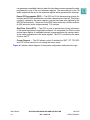
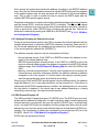
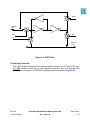
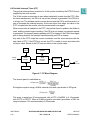
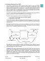
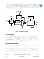
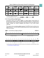
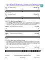
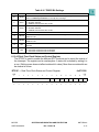
SECTION 6 SYSTEM CONFIGURATION AND PROTECTION The MPC555 incorporates many system functions that normally must be provided in external circuits. In addition, it is designed to provide maximum system safeguards again hardware and/or software faults. The system configuration and protection submodule provides the following features: • System Configuration — The USIU allows the user to configure the system according to the particular requirements. The functions include control of show cycle operation, pin multiplexing, and internal memory map location. System configuration also includes a register containing part and mask number constants to identify the part in software. • Interrupt Configuration — The interrupt controller receives interrupt requests from a number of internal and external sources and directs them on a single interrupt-request line to the RCPU. • General-Purpose I/O — The USIU provides 64 pins for general-purpose I/O. The SGPIO pins are multiplexed with the address and data pins. • External Master Modes Support — External master modes are special modes of operation that allow an alternate master on the external bus to access the internal modules for debugging and backup purposes. • Bus Monitor — The SIU provides a bus monitor to watch internal to external accesses. It monitors the transfer acknowledge (TA) response time for internal to external transfers. A transfer error acknowledge (TEA) is asserted if the TA response limit is exceeded. This function can be disabled. • Software Watchdog Timer (SWT) — The SWT asserts a reset or non-maskable interrupt (as selected by the system protection control register) if the software fails to service the SWT for a designated period of time (e.g, because the software is trapped in a loop or lost). After a system reset, this function is enabled with a maximum time-out period and asserts a system reset if the time-out is reached. The SWT can be disabled or its time-out period can be changed in the SYPCR. Once the SYPCR is written, it cannot be written again until a system reset. • Periodic Interrupt Timer (PIT) — The SIU provides a timer to generate periodic interrupts for use with a real-time operating system or the application software. The PIT provides a period from 1 µs to 4 seconds with a 4-Mhz crystal or 200 ns to 0.8 ms with a 20-Mhz crystal. The PIT function can be disabled. • Power-PC Time Base Counter (TB) — The TB is a 64-bit counter defined by the MPC555 architecture to provide a time base reference for the operating system or application software. The TB has four independent reference registers which MPC555 USER’S MANUAL SYSTEM CONFIGURATION AND PROTECTION Rev. 15 Nov 98 MOTOROLA 6-1 can generate a maskable interrupt when the time-base counter reaches the value programmed in one of the four reference registers. The associated bit in the TB status register will be set for the reference register which generated the interrupt. • Power-PC Decrementer (DEC) — The DEC is a 32-bit decrementing counter defined by the MPC555 architecture to provide a decrementer interrupt. This binary counter is clocked by the same frequency as the time base (also defined by the MPC555 architecture). The period for the DEC when driven by a 4-Mhz oscillator is 4295 seconds, which is approximately 71.6 minutes. • Real-Time Clock (RTC) — The RTC is used to provide time-of-day information to the operating system or application software. It is composed of a 45-bit counter and an alarm register. A maskable interrupt is generated when the counter reaches the value programmed in the alarm register. The RTC is clocked by the same clock as the PIT. • Freeze Support — The SIU allows control of whether the SWT, PIT, TB, DEC and RTC should continue to run during the freeze mode. Figure 6-1 shows a block diagram of the system configuration and protection logic. MOTOROLA 6-2 SYSTEM CONFIGURATION AND PROTECTION Rev. 15 Nov 98 MPC555 USER’S MANUAL Module Configuration Interrupt Controller TEA Signal Bus Monitor Clock Periodic Interrupt Timer Interrupt Software Watchdog Timer Interrupt or System Reset MPC555 Decrementer Decrementer Exception MPC555 Time Base Counter Interrupt Real-Time Clock Interrupt Figure 6-1 System Configuration and Protection Logic 6.1 System Configuration The SIU allows the user to configure the system according to the particular requirements. The functions include control of show cycle operation, pin multiplexing, and internal memory map location. System configuration also includes a register containing part and mask number constants to identify the part in software. System configuration registers include the system configuration register (SIUMCR), the internal memory mapping register (IMMR). Refer to 6.13 System Configuration and Protection Registers for register diagrams and bit descriptions. MPC555 USER’S MANUAL SYSTEM CONFIGURATION AND PROTECTION Rev. 15 Nov 98 MOTOROLA 6-3 6.1.1 USIU Pins Multiplexing Some of the functions defined in the various sections of the SIU (external bus interface, memory controller, and general-purpose I/O) share pins. Table 6-1 summarizes how the pin functions of these multiplexed pins are assigned. . Table 6-1 USIU Pins Multiplexing Control Pin Name Multiplexing Controlled By: IRQ0/SGPIOC0 IRQ1/RSV/SGPIOC1 IRQ2/CR/SGPIOC2/MTS IRQ3/KR/RETRY/SGPIOC3 IRQ4/AT2/SGPIOC4 IRQ5/SGPIOC5/MODCK1 IRQ6/MODCK2 IRQ7/MODCK3 At Power-on reset: MODCK[1:3] Otherwise: programmed in SIUMCR SGPIOC6/FRZ/PTR SGPIOC7/IRQ_OUT/LWP0 BG/VF0/LWP1 BR/VF1/IWP2 BB/VF2/IWP3 IWP[0:1]/VFLS[0:1] BI/STS WE(0:3)/BE(0:3)/AT(0:3) TDI/DSDI TCK/DSCK TDO/DSDO Programmed in SIUMCR and hard reset configuration DATA[0:31]/SGPIOD[0:31] ADDR[8:31]/SGPIOA[8:31] Programmed in SIUMCR RSTCONF/TEXP At Power-on reset: RSTCONF Otherwise: programmed in SIUMCR 6.1.2 Memory Mapping The MPC555 internal memory space can be assigned to one of eight locations. The internal memory map is organized as a single 4-Mbyte block. The user can assign this block to one of eight locations by programming the ISB field in the internal memory mapping register (IMMR). The eight possible locations are the first eight 4-Mbyte memory blocks starting with address 0x0000 0000. (Refer to Figure 6-2.) MOTOROLA 6-4 SYSTEM CONFIGURATION AND PROTECTION Rev. 15 Nov 98 MPC555 USER’S MANUAL 0x0000 0000 0x003F FFFF 0x0040 0000 0X007F FFFF 0X0080 0000 0x00BF FFFF 0x00C0 0000 Internal 4-Mbyte Memory Block (Resides in one of eight locations) 0x00FF FFFF 0x0100 0000 0x013F FFFF 0x0140 0000 0x017F FFFF 0x0180 0000 0x01BF FFFF 0x01C0 0000 0x01FF FFFF 0xFFFF FFFF Figure 6-2 MPC555 Memory Map 6.1.3 Arbitration Support Two bits in the SIUMCR control USIU bus arbitration. The external arbitration (EARB) bit determines whether arbitration is performed internally or externally. If EARB is cleared (internal arbitration), the external arbitration request priority (EARP) bit determines the priority of an external master’s arbitration request. The operation of the internal arbiter is described in 9.5.6.4 Internal Bus Arbiter. 6.2 External Master Modes External master modes are special modes of operation that allow an alternate master on the external bus to access the internal modules for debugging and backup purMPC555 USER’S MANUAL SYSTEM CONFIGURATION AND PROTECTION Rev. 15 Nov 98 MOTOROLA 6-5 poses. They provide access to the internal buses (U-bus and L-bus) and to the intermodule bus (IMB3). There are two external master modes. Peripheral mode (enabled by setting PRPM in the EMCR) is a special slave mechanism in which the RCPU is shut down and an alternate master on the external bus can perform accesses to any internal bus slave. Slave mode (enabled by setting SLVM and clearing PRPM in the EMCR) enables an external master to access any internal bus slave while the RCPU is fully operational. Both modes can be enabled and disabled by software. In addition, peripheral mode can be selected from reset. The internal bus is not capable of providing fair priority between internal RCPU accesses and external master accesses. If the bandwidth of external master accesses is large, it is recommended that the system forces gaps between external master accesses in order to avoid suspension of internal RCPU activity. The MPC555 does not support burst accesses from an external master; only single accesses of 8, 16, or 32 bits can be performed. The MPC555 asserts burst inhibit (BI) on any attempt to initiate a burst access to internal memory. The MPC555 provides memory controller services for external master accesses (single and burst) to external memories. See SECTION 10 MEMORY CONTROLLER for details. 6.2.1 Operation of External Master Modes The external master modes are controlled by the EMCR register, which contains the internal bus attributes. The default attributes in the EMCR enable the external master to configure EMCR with the required attributes, and then access the internal registers. The external master must be granted external bus ownership in order to initiate the external master access. The SIU compares the address on the external bus to the allocated internal address space. If the address is within the internal space, the access is performed with the internal bus. The internal address space is determined according to ISB (see 6.13.1.2 Internal Memory Map Register for details). The external master access is terminated by the TA, TEA or RETRY signal on the external bus. A deadlock situation might occur if an internal-to-external access is attempted on the internal bus while an external master access is initiated on the external bus. In this case, the SIU will assert the RETRY on the external bus in order to relinquish and retry the external access until the internal access is completed. The internal bus will deny other internal accesses for the next eight clocks in order to complete the pending accesses and prevent additional internal accesses from being initiated on the internal bus. The SIU will also mask internal accesses to support consecutive external accesses if the delay between the external accesses is less than 4 clocks. The external master access and retry timings are described in 9.5.11 Bus Operation in External Master Modes. The external master may access the internal MPC555 special registers that are located outside the RCPU. In order to access one of these MPC555 registers, program the EMCR to MPC555 special register access (CONT = 1 and SUPU = 0 in EMCR). MOTOROLA 6-6 SYSTEM CONFIGURATION AND PROTECTION Rev. 15 Nov 98 MPC555 USER’S MANUAL Next, access the register by providing the address according to the MPC555 address map. Only the first external master access that follows EMCR setting will be assigned to the special register map; the next accesses will be directed to the normal address map. This is done in order to enable the user to access the EMCR again after the required MPC555 special register access. Peripheral mode does not require external bus arbitration between the external master and the internal RCPU, since the internal RCPU is disabled. The BR and BB signals should be connected to ground, and the internal bus arbitration should be selected in order to prevent the “slave” MPC555 from occupying the external bus. Internal bus arbitration is selected by clearing the EARB bit in the SIUMCR (see 6.13.1.1 SIU Module Configuration Register). 6.2.2 Address Decoding for External Accesses During an external master access, the USIU compares the external address with the internal address block to determine if MPC555 operation is required. Since only 24 of the 32 internal address bits are available on the external bus, the USIU assigns zeros to the most significant address bits (ADDR[0:7]). The address compare sequence can be summarized as follows: • Normal external access. If the CONT bit in EMCR is cleared, the address is compared to the internal address map. • MPC555 special register external access. If the CONT bit in EMCR is set by the previous external master access, the address is compared to the MPC555 special address range. See 5.4 USIU PowerPC Memory Map for a list of the SPRs in the USIU. • Memory controller external access. If the first two comparisons do not match, the internal memory controller determines whether the address matches an address assigned to one of the regions. If it finds a match, the memory controller generates the appropriate chip select and attribute accordingly When trying to fetch an MPC555 special register from an external master, the address might be aliased to one of the external devices on the external bus. If this device is selected by the MPC555 internal memory controller, this aliasing does not occur since the chip select is disabled. If the device has its own address decoding or is being selected by external logic, this case should be resolved. 6.3 USIU General-Purpose I/O The USIU provides 64 general-purpose I/O (SGPIO) pins. The SGPIO pins are multiplexed with the address and data pins. In single-chip mode, where communicating with external devices is not required, the user can use all 64 SGPIO pins. In multiple-chip mode, only eight SGPIO pins are available. Another configuration allows the use of the address bus for instruction show cycles while the data bus is dedicated to SGPIO functionality. The functionality of these pins is assigned by the single-chip (SC) bit in the SIUMCR. (See 6.13.1.1 SIU Module Configuration Register.) SGPIO pins are grouped as follows: MPC555 USER’S MANUAL SYSTEM CONFIGURATION AND PROTECTION Rev. 15 Nov 98 MOTOROLA 6-7 • Six groups of eight pins each, whose direction is set uniformly for the whole group • 16 single pins whose direction is set separately for each pin Table 6-2 describes the SGPIO signals, and all available configurations. The SGPIO registers are described in 6.13.5 General-Purpose I/O Registers. Table 6-2 SGPIO Configuration SGPIO Group Name Individual Pin Control Available Available Available Available When SC = 10 When SC = 00 When SC = 01 When SC = 11 (Single-Chip (32-bit Port (16-bit Port (Single-Chip Mode with Size Mode) Size Mode) Mode) Trace) Direction Control SGPIOD[0:7] GDDR0 SGPIOD[8:15] GDDR1 SGPIOD[16:23] GDDR2 X X SDDRD[23:31] X X SDDRC[0:7] SGPIOD[24:31] SGPIOC[0:7] 1 X X X X X X X X SGPIOA[8:15] GDDR3 X SGPIOA[16:23] GDDR4 X SGPIOA[24:31] GDDR5 X NOTES: 1. SGPIOC[0:7] is selected according to GPC and MLRC fields in SIUMCR. See 6.13.1.1 SIU Module Configuration Register. Figure 6-3 illustrates the functionality of the SGPIO. MOTOROLA 6-8 SYSTEM CONFIGURATION AND PROTECTION Rev. 15 Nov 98 MPC555 USER’S MANUAL Read Internal Bus Write OE Clk SGPIO Pad Figure 6-3 SGPIO Cell 6.4 Interrupt Controller The USIU receives interrupts from internal sources (such as the PIT and RTC), from the IMB3 module (which has its own interrupt controller), and from external pins IRQ[0:7]. An overview of the MPC555 interrupt structure is shown in Figure 6-4. MPC555 USER’S MANUAL SYSTEM CONFIGURATION AND PROTECTION Rev. 15 Nov 98 MOTOROLA 6-9 IRQ[0:7] Edge Detect SWT Selector NMI Generate IRQ0 NMI DEC DEC Level 7 8 TB 17 Level 6 PIT 16 15 IMB3 Interrupt Levels 8 RTC Level 4 14 32 Change of Lock 8 RCPU Level 5 Level 3 13 Interrupt Controller 8 IREQ Level 2 12 8 UIMB Level 1 IMB3 Interrupts: 11 IRQ[0:6] →Level 0:6 Level 0 IRQ[7:31] →Level 7 10 Debug Debug SIU IRQOUT Figure 6-4 MPC555 Interrupt Structure If programmed to generate interrupts, the SWT and external pin IRQ0 always generate a non-maskable interrupt (NMI) to the RCPU. Notice that the RCPU takes the system reset interrupt when an NMI is asserted and the external interrupt for any other interrupt asserted by the interrupt controller. Each one of the external pins IRQ[1:7] has its own dedicated assigned priority level. IRQ0 is also mapped but should be used only as a status bit indicating that IRQ0 was asserted and generated an NMI interrupt. There are eight additional interrupt priority MOTOROLA 6-10 SYSTEM CONFIGURATION AND PROTECTION Rev. 15 Nov 98 MPC555 USER’S MANUAL levels. Each one of the SIU internal interrupt sources, as well as the interrupt requests generated by the IMB3 modules, can be assigned by the software to any one of those eight interrupt priority levels. The same interrupt request signal that is generated within the RCPU is optionally driven on the IRQ_OUT pin. This pin may be used in peripheral mode, in which the internal processor is shut off and the internal modules are accessed externally. The IMB3 interrupts are controlled by the UIMB. The IMB3 provides 32 interrupt levels. Any interrupt source can be configured to any IMB3 interrupt level. The 32-bit UIPEND register in the UIMB holds the pending IMB3 interrupt requests. IMB3 interrupt request levels zero to six are mapped to USIU interrupt levels zero to six, respectively. IMB3 interrupt request levels seven to 31 are mapped to USIU request level seven. The user must read the UIPEND register to determine the actual source of the interrupt. Refer to 12.4 Interrupt Operation for more information. NOTE If the same interrupt level is assigned to more than one source, software must read the appropriate status bits in the appropriate UIMB3 registers to determine which interrupt was asserted. Figure 6-5 illustrates the operation of the interrupt controller. MPC555 USER’S MANUAL SYSTEM CONFIGURATION AND PROTECTION Rev. 15 Nov 98 MOTOROLA 6-11 . IRQ[0:7] IRQ0 NMI to RCPU Interrupt Level (0-7) 8 Interrupt Vector Highest S I V E C Priority Interrupt Detector (1 from 16) (Enables Branch to the Highest Priority Interrupt Routine) SIPEND SIMASK Interrupt Request (to RCPU and Pads) latch Figure 6-5 MPC555 Interrupt Configuration 6.4.1 SIU Interrupt Sources Priority The SIU has 15 interrupt sources that assert just one interrupt request to the RCPU. There are eight external IRQ pins (IRQ0 should be masked since it generates a NMI) and eight interrupt levels. The priority between all interrupt sources is shown in Table 6-3. MOTOROLA 6-12 SYSTEM CONFIGURATION AND PROTECTION Rev. 15 Nov 98 MPC555 USER’S MANUAL Table 6-3 Priority of Interrupt Sources Priority Interrupt Source Interrupt Code 0 (Highest) IRQ0 00000000 1 Level 0 00000100 2 IRQ1 00001000 3 Level 1 00001100 4 IRQ2 00010000 5 Level 2 00010100 6 IRQ3 00011000 7 Level 3 00011100 8 IRQ4 00100000 9 Level 4 00100100 10 IRQ5 00101000 11 Level 5 00101100 12 IRQ6 00110000 13 Level 6 00110100 14 IRQ7 00111000 15 (Lowest) Level 7 00111100 16-31 Reserved — 6.5 Hardware Bus Monitor The bus monitor ensures that each bus cycle is terminated within a reasonable period of time. The USIU provides a bus monitor option to monitor internal to external bus accesses on the external bus. The monitor counts from transfer start to transfer acknowledge and from transfer acknowledge to transfer acknowledge within bursts. If the monitor times out, transfer error acknowledge (TEA) is asserted internally. The bus monitor timing bit in the system protection control register (SYPCR) defines the bus monitor time-out period. The programmability of the time-out allows for variation in system peripheral response time. The timing mechanism is clocked by the system clock divided by eight. The maximum value is 2040 system clock cycles. The bus monitor enable (BME) bit in the SYPCR enables or disables the bus monitor. The bus monitor is always enabled, however, when freeze is asserted or when a debug mode request is pending, regardless of the state of this bit. 6.6 MPC555 Decrementer The decrementer (DEC) is a 32-bit decrementing counter defined by the MPC555 architecture to provide a decrementer interrupt. This binary counter is clocked by the same frequency as the time base (also defined by the MPC555 architecture). The operation of the time base and decrementer are therefore coherent. In the MPC555, the DEC is clocked by the TMBCLK clock. The decrementer period is computed as follows: MPC555 USER’S MANUAL SYSTEM CONFIGURATION AND PROTECTION Rev. 15 Nov 98 MOTOROLA 6-13 2 32 T dec = -----------------Ftmbclk The state of the DEC is not affected by any resets and should be initialized by software. The DEC runs continuously after power-up once the time base is enabled by setting the TBE bit of the TBSCR (see Table 6-16) (unless the clock module is programmed to turn off the clock). The decrementer continues counting while reset is asserted. Loading from the decrementer has no effect on the counter value. Storing to the decrementer replaces the value in the decrementer with the value in the GPR. Whenever bit zero (the MSB) of the decrementer changes from zero to one, a decrementer exception occurs. If software alters the decrementer such that the content of bit 0 is changed to bit 1, a decrementer exception occurs. A decrementer exception causes a decrementer interrupt request to be pending in the RCPU. When the decrementer interrupt is taken, the decrementer interrupt request is automatically cleared. Table 6-4 illustrates some of the periods available for the decrementer, assuming a 4 MHz or 20 MHz crystal, and TBS = 0 which selects tbclk division to FOUR. Table 6-4 Decrementer Time-Out Periods Count Value Time-Out @ 4 MHz Time-Out @ 20 MHz 0 1.0 µs 0.2 µs 9 10 µs 2.0 µs 99 100 µs 20 µs 999 1.0 ms 200 µs 9999 10.0 ms 2 ms 999999 1.0 s 200 ms 9999999 10.0 s 2.0 s 99999999 100.0 s 20 s 999999999 1000. s 200 s (hex) FFFFFFFF 4295 s 859 s Refer to 3.9.5 Decrementer Register (DEC) for more information. 6.7 MPC555 Time Base (TB) The time base (TB) is a 64-bit free-running binary counter defined by the MPC555 architecture. The TB has two independent reference registers which can generate a maskable interrupt when the time base counter reaches the value programmed in one of the two reference registers. The period of the TB depends on the driving frequency. In the MPC555, the TB is clocked by the TMBCLK clock. The period for the TB is: MOTOROLA 6-14 SYSTEM CONFIGURATION AND PROTECTION Rev. 15 Nov 98 MPC555 USER’S MANUAL T 2 64 = ----------------------TB F tmbclk The state of the time base is not affected by any resets and should be initialized by software. Reads and writes of the TB are restricted to special instructions. Separate special-purpose registers are defined in the MPC555 architecture for reading and writing the time base. For the MPC555 implementation, it is not possible to read or write the entire TB in a single instruction. Therefore, the mttb and mftb instructions are used to move the lower half of the time base (TBL) while the mttbu and mftbu instructions are used to move the upper half (TBU). Two reference registers are associated with the time base: TBREFF0 and TBREFF1. A maskable interrupt is generated when the TB count reaches to the value programmed in one of the two reference registers. Two status bits in the time base control and status register (TBSCR) indicate which one of the two reference registers generated the interrupt. Refer to 6.13.4 System Timer Registers for diagrams and bit descriptions of time base registers. Refer to 3.9.4 Time Base Facility (TB) — OEA and to RCPU Reference Manual (RCPURM/AD) for additional information regarding the MPC555 time base. 6.8 Real-Time Clock (RTC) The RTC is a 32-bit counter and pre-divider used to provide a time-of-day indication to the operating system and application software. It is clocked by the pitrtclk clock.The counter is not affected by reset and operates in all low-power modes. It is initialized by software. The RTC can be programmed to generate a maskable interrupt when the time value matches the value programmed in its associated alarm register. It can also be programmed to generate an interrupt once a second. A control and status register is used to enable or disable the different functions and to report the interrupt source. FREEZE Sec Interrupt RTSEC pitrtclk Clock Clock Disable Divide By 15625 32-bit Counter (RTC) MUX Divide By 78125 = Alarm Interrupt 4-MHz / 20-MHz crystal 32-bit Register (RTCAL) Figure 6-6 RTC Block Diagram MPC555 USER’S MANUAL SYSTEM CONFIGURATION AND PROTECTION Rev. 15 Nov 98 MOTOROLA 6-15 6.9 Periodic Interrupt Timer (PIT) The periodic interrupt timer consists of a 16-bit counter clocked by the PITRCLK clock supplied by the clock module. The 16-bit counter counts down to zero when loaded with a value from the PITC. After the timer reaches zero, the PS bit is set and an interrupt is generated if the PIE bit is is a logic one. The software service routine should read the PS bit and then write it to zero to terminate the interrupt request. At the next input clock edge, the value in the PITC is loaded into the counter, and the process starts over again. When a new value is loaded into the PITC, the periodic timer is updated, the divider is reset, and the counter begins counting. If the PS bit is not cleared, an interrupt request is generated. The request remains pending until PS is cleared. If the PS bit is set again prior to being cleared, the interrupt remains pending until PS is cleared. Any write to the PITC stops the current countdown, and the count resumes with the new value in PITC. If the PTE bit is not set, the PIT is unable to count and retains the old count value. Reads of the PIT have no effect on the counter value. PTE PITC (PISCR) (PISCR) pitrtclk Clock Clock Disable 16-bit Modulus Counter PS (PISCR) PIT Interrupt PIE (PISCR) PITF (PISCR) Figure 6-7 PIT Block Diagram The timeout period is calculated as: PIT period PITC + 1 PITC + 1 = ------------------------ = ----------------------------------------------F ExternalClock pitrtclk ----------------------------- 4or256 Solving this equation using a 4-MHz external clock and a pre-divider of 256 gives: PITC + 1 PITperiod = -----------------------15625 This gives a range from 64 microseconds, with a PITC of 0x0000, to 4.19 seconds, with a PITC of 0xFFFF. When a 20-MHz crystal is used with a pre-divider of 256, the range is between 12.8 microseconds to 0.84 seconds. MOTOROLA 6-16 SYSTEM CONFIGURATION AND PROTECTION Rev. 15 Nov 98 MPC555 USER’S MANUAL 6.10 Software Watchdog Timer (SWT) The software watchdog timer (SWT) prevents system lockout in case the software becomes trapped in loops with no controlled exit. The SWT is enabled after system reset to cause a system reset if it times out. it. The SWT requires a special service sequence to be executed on a periodic basis. If this periodic servicing action does not occur, the SWT times out and issues a reset or a non-maskable interrupt (NMI), depending on the value of the SWRI bit in the SYPCR. The SWT can be disabled by clearing the SWE bit in the SYPCR. Once the SYPCR is written by software, the state of the SWE bit cannot be changed. The SWT service sequence consists of the following two steps: 1. Write 0x556C to the Software Service Register (SWSR) 2. Write 0xAA39 to the SWSR The service sequence clears the watchdog timer and the timing process begins again. If any value other than 0x556C or 0xAA39 is written to the SWSR, the entire sequence must start over. Although the writes must occur in the correct order prior to time-out, any number of instructions may be executed between the writes. This allows interrupts and exceptions to occur, if necessary, between the two writes. Not 0x556C / Don’t Reload Reset 0x556C / Don’t Reload State 0 Waiting for 0x556C State 1 Waiting for 0xAA39 0xAA39 / Reload Not 0x556C / Don’t Reload Not 0xAA39 / Don’t Reload Although most software disciplines support the watchdog concept, different systems require different time-out periods. For this reason, the software watchdog provides a selectable range for the time-out period. In Figure 6-8, the range is determined by the value SWTC field. The value held in the SWTC field is then loaded into a 16-bit decrementer clocked by the system clock. An additional divide by 2048 prescaler is used if necessary. The decrementer begins counting when loaded with a value from the software watchdog timing count field (SWTC). After the timer reaches 0x0, a software watchdog expiration request is issued to the reset or NMI control logic. MPC555 USER’S MANUAL SYSTEM CONFIGURATION AND PROTECTION Rev. 15 Nov 98 MOTOROLA 6-17 Upon reset, the value in the SWTC is set to the maximum value and is again loaded into the software watchdog register (SWR), starting the process over. When a new value is loaded into the SWTC, the software watchdog timer is not updated until the servicing sequence is written to the SWSR. If the SWE is loaded with the value zero, the modulus counter does not count. SWSR SWE (SYPCR) System Clock Clock Disable Service Logic SWTC Divide By 2048 Reload MUX 16-bit SWR / Decrementer Rollove = 0 Reset or NMI FREEZE Time-out SWP (SYPCR) Figure 6-8 SWT Block Diagram 6.11 Freeze Operation When the FREEZE line is asserted, the clocks to the software watchdog, the periodic interrupt timer, the real-time clock, the time base counter, and the decrementer can be disabled. This is controlled by the associated bits in the control register of each timer. If programmed to stop during FREEZE assertion, the counters maintain their values while FREEZE is asserted, unless changed by the software. The bus monitor, however, remains enabled regardless of this signal. 6.12 Low Power Stop Operation When the processor is set in a low-power mode (doze, sleep, or deep sleep), the software watchdog timer is frozen. It remains frozen and maintain its count value until the processor exits this state and resumes executing instructions. The periodic interrupt timer, decrementer, and time base are not affected by these lowpower modes. They continue to run at their respective frequencies. These timers are capable of generating an interrupt to bring the MCU out of these low-power modes. MOTOROLA 6-18 SYSTEM CONFIGURATION AND PROTECTION Rev. 15 Nov 98 MPC555 USER’S MANUAL 6.13 System Configuration and Protection Registers This section provides diagrams and bit descriptions of the system configuration and protection registers. 6.13.1 System Configuration Registers System configuration registers include the SIUMCR, the EMCR, and the IMMR. 6.13.1.1 SIU Module Configuration Register The SIU module configuration register (SIUMCR) configures various aspects of SIU operation. SIUMCR — SIU Module Configuration Register MSB 0 1 EARB 2 3 4 5 EARP 6 7 RESERVED 8 0x2F C000 9 10 DSHW DBGC 11 12 13 DBPC ATWC 14 GPC 15 DLK RESET: ID0* 16 RESERVED 0 0 0 0 0 0 0 0 ID[9:10]* 17 18 19 20 21 22 23 24 25 SC RCTX ID[17:18]* 0 MLRC RESERVED 26 ID11* 27 MTSC ID12* 28 0 0 0 29 30 LSB 31 0 0 0 RESERVED RESET: 0 0 0 0 0 0 0 0 0 0 * The reset value is a reset configuration word value, extracted from the indicated internal data bus lines. WARNING Software must not change any SIUMCR fields controlled by the reset configuration word while the functions that these fields control are active. MPC555 USER’S MANUAL SYSTEM CONFIGURATION AND PROTECTION Rev. 15 Nov 98 MOTOROLA 6-19 Table 6-5 SIUMCR Bit Settings Bit(s) Name Description 0 EARB External arbitration 0 = Internal arbitration is performed 1 = External arbitration is assumed 1:3 EARP External arbitration request priority. This field defines the priority of an external master’s arbitration request. This field is valid when EARB is cleared. Refer to 9.5.6.4 Internal Bus Arbiter for details. 4:7 — Reserved 8 DSHW Data show cycles. This bit selects the show cycle mode to be applied to U-bus data cycles (data cycles to IMB modules and flash EEPROM). This field is locked by the DLK bit. Note that instruction show cycles are programmed in the ICTRL and L-bus data show cycles (to SRAM) are programmed in the L2UMCR. 0 = Disable show cycles for all internal data cycles 1 = Show address and data of all internal data cycles 9:10 DBGC Debug pins configuration. Refer to Table 6-6. 11 DBPC Debug port pins configuration. Refer to Table 6-7. 12 ATWC Address write type enable configuration. This bit configures the pins to function as byte write enables or address types for debugging purposes. 0 = WE(0:3)/BE(0:3)/AT(0:3) functions as WE(0:3)/BE(0:3)1 1 = WE(0:3)/BE(0:3)/AT(0:3) functions as AT(0:3) 13:14 GPC This bit configures the pins as shown in Table 6-8. 15 DLK Debug register lock 0 = Normal operation 1 = SIUMCR is locked and can be written only in test mode or when the internal freeze signal is asserted. 16 — Reserved 17:18 SC Single-chip select. This field configures the functionality of the address and data buses. Changing the SC field while external accesses are performed is not supported. Refer to Table 6-9. 19 RCTX Reset configuration/timer expired. During reset the RSTCONF/TEXP pin functions as RSTCONF. After reset the pin can be configured to function as TEXP, the timer expired signal that supports the low-power modes. 0 = RSTCONF/TEXP functions as RSTCONF 1 = RSTCONF/TEXP functions as TEXP 20:21 MLRC Multi-level reservation control. This field selects between the functionality of the reservation logic and IRQ pins, refer to Table 6-10. 22:23 — 24 MTSC 25:31 — Reserved Memory transfer start control. 0 = IRQ2/CR/SGPIOC2/MTS functions as MTS 1 = IRQ2/CR/SGPIOC2/MTS functions according to the MLRC bits setting Reserved NOTES: 1. WE/BE is selected per memory region by WEBS in the approprite BR register in the memory controller. MOTOROLA 6-20 SYSTEM CONFIGURATION AND PROTECTION Rev. 15 Nov 98 MPC555 USER’S MANUAL Table 6-6 Debug Pins Configuration DBGC Pin Function IWP[0:1]/VFLS[0:1] BI/STS BG/VF0/LWP1 BR/VF1/IWP2 BB/VF2/IWP3 VFLS[0:1] BI BG BR BB 01 IWP[0:1] STS BG BR BB 10 VFLS[0:1] STS VF0 VF1 VF2 11 IWP[0:1] STS LWP1 IWP2 IWP3 00 Table 6-7 Debug Port Pins Configuration Pin Function DBPC TCK/DSCK TDI/DSDI TDO/DSDO 0 DSCK DSDI DSDO 1 TCK TDI TDO Table 6-8 General Pins Configuration GPC Pin Function FRZ/PTR/SGPIOC6 IRQOUT/LWP0/SGPIOC7 00 PTR LWP0 01 SGPIOC6 SGPIOC7 10 FRZ LWP0 11 FRZ IRQOUT Table 6-9 Single-Chip Select Field Pin Configuration Pin Function SC DATA[0:15]/ SGPIOD[0:15] DATA[16:31] SGPIOD[16:31] ADDR[8:31]/ SGPIOA[8:31] 00 (multiple chip, 32-bit port size) DATA[0:15] DATA[16:31] ADDR[8:31] 01 (multiple chip, 16-bit port size DATA[0:15] SPGIOD[16:31] ADDR[8:31] 10 (single-chip with address show cycles for debugging) SPGIOD[0:15] SPGIOD[16:31] ADDR[8:31] 11 (single-chip) SPGIOD[0:15] SPGIOD[16:31] SPGIOA[8:31] MPC555 USER’S MANUAL SYSTEM CONFIGURATION AND PROTECTION Rev. 15 Nov 98 MOTOROLA 6-21 Table 6-10 Multi-Level Reservation Control Pin Configuration Pin Function MLRC IRQ2/CR/ IRQ3/KR/RETRY SGPIOC2/MTS /SGPIOC3 IRQ4/AT2/ SGPIOC4 IRQ5/SGPIOC5/ MODCK11 IRQ3 IRQ4 IRQ5 / MODCK1 CR2 KR/RETRY AT2 IRQ5 / MODCK1 SGPIOC1 SGPIOC22 SGPIOC3 SGPIOC4 SGPIOC5/ MODCK1 IRQ1 SGPIOC22 KR/RETRY AT2 SGPIOC5/ MODCK1 IRQ0/SGPIOC0 IRQ1/RSV/ SGPIOC1 00 IRQ0 IRQ1 IRQ22 01 IRQ0 RSV 10 SGPIOC0 11 IRQ0 NOTES: 1. Operates as MODCK1 during reset. 2. This holds if MTSC bit is reset to 0. Otherwise IRQ2/CR/SGPIOC2/MTS will function as MTS. 6.13.1.2 Internal Memory Map Register The internal memory map register (IMMR) is a special register located within the MPC555 special register space. The IMMR contains identification of a specific device as well as the base for the internal memory map. Based on the value read from this register, software can deduce availability and location of any on-chip system resources. This register can be read by the mfspr instruction. The ISB field can be written by the mtspr instruction. The PARTNUM and MASKNUM fields are mask programmed and cannot be changed. IMMR — Internal Memory Mapping Register MSB 0 1 2 3 4 5 6 7 SPR 638 8 9 10 11 12 13 PARTNUM MASKNUM Read-Only Fixed Value Read-Only Fixed Value 14 15 30 LSB 31 RESET: 16 17 18 19 RESERVED 20 FLEN 21 22 RESERVED 23 24 CLES 25 26 27 RESERVED 28 29 ISB 0 ID[28:30]* 0 RESET: 0 0 0 0 ID20* 0 0 ID23* 0 0 0 0 * The reset value is a reset configuration word value extracted from the indicated bits of the internal data bus. Refer to 7.5.2 Hard Reset Configuration Word. MOTOROLA 6-22 SYSTEM CONFIGURATION AND PROTECTION Rev. 15 Nov 98 MPC555 USER’S MANUAL Table 6-11 IMMR Bit Settings Bit(s) Name 0:7 PARTNUM 8:15 MASKNUM 16:19 — 20 FLEN 21:22 — 23 CLES 24:27 — 28:30 ISB 31 — Description This read-only field is mask programmed with a code corresponding to the part number of the part on which the SIU is located. It is intended to help factory test and user code which is sensitive to part changes. This changes when the part number changes. For example, it would change if any new module is added, if the size of any memory module is changed. It would not change if the part is changed to fix a bug in an existing module. The MPC555 chip has an ID of 0x30. This read-only field is mask programmed with a code corresponding to the mask number of the part. It is intended to help factory test and user code which is sensitive to part changes. Reserved Flash enable. The default state of FLEN is negated, meaning that the boot is performed from external memory. This bit can be set at reset by through the reset configuration word. 0 = On-chip flash memory is disabled, and all internal cycles to the allocated flash address space are mapped to external memory 1 = On-chip flash memory is enabled Reserved Core little-endian swap 0 = Little-endian swap logic in the EBI is not activated for RCPU accesses after reset 1 = Little- endian swap logic in the EBI is activated for RCPU accesses after reset Reserved This read-write field defines the base address of the internal memory space. The initial value of this field can be configured at reset to one of eight addresses, and then can be changed to any value by software. Internal base addresses are as follows: 000 = 0x0000 0000 001 = 0x0040 0000 010 = 0x0080 0000 011 = 0x00C0 0000 100 = 0x0100 0000 101 = 0x0140 0000 110 = 0x0180 0000 111 = 0x01C0 0000 Reserved 6.13.1.3 External Master Control Register (EMCR) The external master control register selects the external master modes and determines the internal bus attributes for external-to-internal accesses. EMCR — External Master Control Register MSB 0 1 2 3 4 5 6 7 0x2F C030 8 9 10 11 12 13 14 15 RESERVED RESET: 0 0 0 0 0 0 0 0 0 0 0 0 0 0 0 0 16 17 18 19 20 21 22 23 24 25 26 27 28 29 30 LSB 31 SUPU INST 0 1 PRPM SLVM 0 SIZE RESERVED RESV CONT 0 TRAC SIZEN RESERVED RESET: ID16* 0 0 0 1 0 0 1 1 0 1 1 0 0 * The reset value is a reset configuration word value, extracted from the indicated internal data bus line. Refer to 7.5.2 Hard Reset Configuration Word. MPC555 USER’S MANUAL SYSTEM CONFIGURATION AND PROTECTION Rev. 15 Nov 98 MOTOROLA 6-23 Table 6-12 EMCR Bit Settings Bit(s) Name 0:15 — Description Reserved PRPM Peripheral mode. In this mode, the internal RCPU core is shut off and an alternative master on the external bus can access any internal slave module. The reset value of this bit is determined by the reset configuration word. The bit can also be written by software. 0 = Normal operation 1 = Peripheral mode operation 17 SLVM Slave mode (valid only if PRPM = 0). In this mode, an alternative master on the external bus can access any internal slave module while the internal RCPU core is fully operational. If PRPM is set, the value of SLVN is a “don’t care.” 0 = Normal operation 1 = Slave mode 18 — 16 Reserved 19:20 SIZE Size attribute. If SIZEN = 1, the SIZE bits controls the internal bus attributes as follows: 00 = Double word (4 bytes) 01 = Word (4 bytes) 10 = Half word (2 bytes) 11 = Byte 21 SUPU Supervisor/user attribute. SUPU controls the supervisor/user attribute as follows: 0 = Supervisor mode access permitted to all registers 1 = User access permitted to registers designated “user access” 22 INST Instruction attribute. INST controls the internal bus instruction attribute as follows: 0 = Instruction fetch 1 = Operand or non-CPU access 23:24 — Reserved 25 RESV Reservation attribute. RESV controls the internal bus reservation attribute as follows: 0 = Storage reservation cycle 1 = Not a reservation 26 CONT Control attribute. CONT drives the internal bus control bit attribute as follows: 0 = Access to MPC555 control register, or control cycle access 1 = Access to global address map 27 — Reserved 28 TRAC Trace attribute. TRAC controls the internal bus program trace attribute as follows: 0 = Program trace 1 = Not program trace 29 SIZEN External size enable control bit. SIZEN determines how the internal bus size attribute is driven: 0 = Drive size from external bus signals TSIZE[0:1] 1 = Drive size from SIZE0, SIZE1 in EMCR 30:31 — Reserved 6.13.2 SIU Interrupt Registers The SIU interrupt controller contains the SIPEND, SIMASK, SIEL, and SIVEC registers. 6.13.2.1 SIPEND Register Each of the 32 bits in the SIPEND register corresponds to an interrupt request. The bits associated with internal exceptions indicate, if set, that an interrupt service is requested (if not masked by the corresponding bit in the SIMASK register). Each bit reflects the status of the internal requestor device and is cleared when the appropriate actions are initiated by the software in the device itself. Writing to these bits while they are not set has no effect. MOTOROLA 6-24 SYSTEM CONFIGURATION AND PROTECTION Rev. 15 Nov 98 MPC555 USER’S MANUAL The bits associated with the IRQ pins have a different behavior depending on the sensitivity defined for them in the SIEL register. When the IRQ is defined as a “level” interrupt the corresponding bit behaves similar to the bits associated with internal interrupt sources. When the IRQ is defined as an “edge” interrupt and if the corresponding bit is set, it indicates that a falling edge was detected on the line and the bit can be reset by software by writing a 1 to it. SIPEND — SIU Interrupt Pending Register 0x2F C010 MSB 0 1 2 3 4 5 6 7 8 9 10 11 12 13 14 15 IRQ0 LVL0 IRQ1 LVL1 IRQ2 LVL2 IRQ3 LVL3 IRQ4 LVL4 IRQ5 LVL5 IRQ6 LVL6 IRQ7 LVL7 0 0 0 0 0 0 0 0 0 0 0 0 0 0 0 0 16 17 18 19 20 21 22 23 24 25 26 27 28 29 30 LSB 31 0 0 0 0 0 0 0 RESET: RESERVED RESET: 0 0 0 0 0 0 0 0 0 6.13.2.2 SIU Interrupt Mask Register (SIMASK) The SIMASK is a 32-bit read/write register. Each bit corresponds to an interrupt request bit in the SIPEND register. Setting a bit in this register allows the interrupt request to reach the RCPU. SIMASK is updated by the software and cleared upon reset. It is the responsibility of the software to determine which of the interrupt sources are enabled at a given time. SIMASK — SIU Interrupt Mask Register MSB 0 1 IRM0* LVM0 0x2F C014 2 3 4 5 6 7 8 9 10 11 12 13 14 15 IRM1 LVM1 IRM2 LVM2 IRM3 LVM3 IRM4 LVM4 IRM5 LVM5 IRM6 LVM6 IRM7 LVM7 RESET: 0 0 0 0 0 0 0 0 0 0 0 0 0 0 0 0 16 17 18 19 20 21 22 23 24 25 26 27 28 29 30 LSB 31 0 0 0 0 0 0 0 RESERVED RESET: 0 0 0 0 0 0 0 0 0 *IRQ0 of the SIPEND register is not affected by the setting or clearing of the IRM0 bit of the SIMASK register. IRQ0 is a non-maskable interrupt. MPC555 USER’S MANUAL SYSTEM CONFIGURATION AND PROTECTION Rev. 15 Nov 98 MOTOROLA 6-25 6.13.2.3 SIU Interrupt Edge Level Register (SIEL) The SIEL is a 32-bit read/write register. Each pair of bits corresponds to an external interrupt request. The EDx bit, if set, specifies that a falling edge in the corresponding IRQ line will be detected as an interrupt request. When the EDx bit is 0, a low logical level in the IRQ line will be detected as an interrupt request. The WMx (wake-up mask) bit, if set, indicates that an interrupt request detection in the corresponding line causes the MPC555 to exit low-power mode. SIEL — SIU Interrupt Edge Level Register 0x2F C018 MSB 0 1 2 3 4 5 6 7 8 9 10 11 12 13 14 15 ED0 WM0 ED1 WM1 ED2 WM2 ED3 WM3 ED4 WM4 ED5 WM5 ED6 WM6 ED7 WM7 0 0 0 0 0 0 0 0 0 0 0 0 0 0 0 0 16 17 18 19 20 21 22 23 24 25 26 27 28 29 30 LSB 31 0 0 0 0 0 0 0 RESET: RESERVED RESET: 0 0 0 0 0 0 0 0 0 6.13.2.4 SIU Interrupt Vector Register The SIVEC is a 32-bit read-only register that contains an 8-bit code representing the unmasked interrupt source of the highest priority level. The SIVEC can be read as either a byte, half word, or word. When read as a byte, a branch table can be used in which each entry contains one instruction (branch). When read as a half-word, each entry can contain a full routine of up to 256 instructions. The interrupt code is defined such that its two least significant bits are 0, thus allowing indexing into the table. SIVEC — SIU Interrupt Vector MSB 0 1 2 3 4 5 0x2F C01C 6 7 8 9 10 INTERRUPT CODE 11 12 13 14 15 RESERVED RESET: 0 0 0 0 0 0 0 0 0 0 0 0 0 0 0 0 16 17 18 19 20 21 22 23 24 25 26 27 28 29 30 LSB 31 0 0 0 0 0 0 0 RESERVED RESET: 0 0 MOTOROLA 6-26 0 0 0 0 0 0 0 SYSTEM CONFIGURATION AND PROTECTION Rev. 15 Nov 98 MPC555 USER’S MANUAL 6.13.3 System Protection Registers 6.13.3.1 System Protection Control Register (SYPCR) The system protection control register (SYPCR) controls the system monitors, the software watchdog period, and the bus monitor timing. This register can be read at any time, but can be written only once after system reset. SYPCR — System Protection Control Register MSB 0 1 2 3 4 5 6 7 0x2F C004 8 9 10 11 12 13 14 15 SWTC RESET: 1 1 1 1 1 1 1 1 1 1 1 1 1 1 1 1 16 17 18 19 20 21 22 23 24 25 26 27 28 29 30 LSB 31 SWF SWE SWRI SWP 0 1 1 1 BMT BME RESERVED RESET: 1 1 1 1 1 1 1 1 0 0 0 0 Table 6-13 SYPCR Bit Settings Bit(s) Name Description 0:15 SWTC 16:23 BMT Bus monitor timing. This field specifies the time-out period, in eight-system-clock resolution, of the bus monitor. 24 BME Bus monitor enable 0 = Disable bus monitor 1 = Enable bus monitor 25:27 — Software watchdog timer count. This field contains the count value of the software watchdog timer. Reserved SWF Software watchdog freeze 0 = Software watchdog continues to run while FREEZE is asserted 1 = Software watchdog stops while FREEZE is asserted 29 SWE Software watchdog enable. Software should clear this bit after a system reset to disable the SWT. 0 = Watchdog is disabled 1 = Watchdog is enabled 30 SWRI Software watchdog reset/interrupt select 0 = Software watchdog time-out causes a non-maskable interrupt to the RCPU 1 = Software watchdog time-out causes a system reset 31 SWP Software watchdog prescale 0 = Software watchdog timer is not pre-scaled 1 = Software watchdog timer is prescaled by 2048 28 6.13.3.2 Software Service Register (SWSR) The SWSR is the location to which the SWT servicing sequence is written. To prevent SWT time-out, the user should write a 0x556C followed by 0xAA39 to this register. The SWSR can be written at any time but returns all zeros when read. MPC555 USER’S MANUAL SYSTEM CONFIGURATION AND PROTECTION Rev. 15 Nov 98 MOTOROLA 6-27 SWSR — Software Service Register MSB 0 1 2 3 4 5 0x2F C00E 6 7 8 9 10 11 12 13 14 LSB 15 0 0 0 0 0 0 0 0 SWSR RESET: 0 0 0 0 0 0 0 0 Table 6-14 SWSR Bit Settings Bit(s) Name 0:15 SWSR Description SWT servicing sequence is written to this register. To prevent SWT time-out, the user should write a 0x556C followed by 0xAA39 to this register. The SWSR can be written at any time but returns all zeros when read. 6.13.3.3 Transfer Error Status Register (TESR) The transfer error status register contains a bit for each exception source generated by a transfer error. A bit set to logic 1 indicates what type of transfer error exception occurred since the last time the bits were cleared by reset or by the normal software status bit-clearing mechanism. Note that these bits may be set due to canceled speculative accesses which do not cause an interrupt. The register has two identical sets of bit fields; one is associated with instruction transfers and the other with data transfers. TESR — Transfer Error Status Register MSB 0 1 2 3 4 5 6 0x2F C020 7 8 9 10 11 12 13 14 15 RESERVED RESET: 0 0 0 0 0 0 0 0 0 0 0 0 0 0 0 0 16 17 18 19 20 21 22 23 24 25 26 27 28 29 30 LSB 31 IEXT IBMT DEXT DBM 0 0 0 0 RESERVED RESERVED RESERVED RESET: 0 0 MOTOROLA 6-28 0 0 0 0 0 0 SYSTEM CONFIGURATION AND PROTECTION Rev. 15 Nov 98 0 0 0 0 MPC555 USER’S MANUAL Table 6-15 TESR Bit Settings Bit(s) Name Description 0:17 — 18 IEXT Instruction external transfer error acknowledge. This bit is set if the cycle was terminated by an externally generated TEA signal when an instruction fetch was initiated. 19 IBMT Instruction transfer monitor time out. This bit is set if the cycle was terminated by a bus monitor time-out when an instruction fetch was initiated. 20:25 — 26 DEXT Data external transfer error acknowledge. This bit is set if the cycle was terminated by an externally generated TEA signal when a data load or store is requested by an internal master. 27 DBM Data transfer monitor time out. This bit is set if the cycle was terminated by a bus monitor timeout when a data load or store is requested by an internal master. 28:31 — Reserved Reserved Reserved 6.13.4 System Timer Registers The following sections describe registers associated with the system timers. These facilities are powered by the KAPWR and can preserve their value when the main power supply is off. Refer to 8.3.3 Pre-Divider for details on the required actions needed in order to guarantee this data retention. 6.13.4.1 Decrementer Register The 32-bit decrementer register is defined by the MPC555 architecture. The values stored in this register are used by a down counter to cause decrementer exceptions. The decrementer causes an exception whenever bit zero changes from a logic zero to a logic one. A read of this register always returns the current count value from the down counter. Contents of this register can be read or written to by the mfspr or the mtspr instruction. This register is not affected by reset. The decrementer is powered by standby power and can continue to count when standby power is applied. DEC — Decrementer Register SPR 22 MSB 0 LSB 31 Decrementing Counter RESET: UNCHANGED Refer to 3.9.5 Decrementer Register (DEC) for more information on this register. 6.13.4.2 Time Base SPRs The TB is a 64-bit register containing a 64-bit integer that is incremented periodically. There is no automatic initialization of the TB; the system software must perform this initialization. The contents of the register may be written by the mttbl or the mttbu instructions, see 3.9.4 Time Base Facility (TB) — OEA. MPC555 USER’S MANUAL SYSTEM CONFIGURATION AND PROTECTION Rev. 15 Nov 98 MOTOROLA 6-29 Refer to 3.8 PowerPC VEA Register Set — Time Base and 3.9.4 Time Base Facility (TB) — OEA for more information on reading and writing the TBU and TBL registers. TB — Time Base (Reading) SPR 268, 269 MSB 0 LSB 63 31 32 TBU TBL RESET: UNCHANGED TB — Time Base (Writing) SPR 284, 285 MSB 0 LSB 63 31 32 TBU TBL RESET: UNCHANGED 6.13.4.3 Time Base Reference Registers Two reference registers (TBREFF0 and TBREFF1) are associated with the lower part of the time base (TBL). Each is a 32-bit read/write register. Upon a match between the contents of TBL and the reference register, a maskable interrupt is generated. TBREF0 — Time Base Reference Register 0 0x2F C204 MSB 0 LSB 31 TBREF0 RESET: TBREF1 — Time Base Reference Register 1 0x2F C208 MSB 0 LSB 31 TBREF1 RESET: 6.13.4.4 Time Base Control and Status Register The TBSCR is 16-bit read/write register. It controls the TB, decrementer count enable, and interrupt generation and is used for reporting the source of the interrupts. The register can be read anytime. A status bit is cleared by writing a one to it. (Writing a zero has no effect.) More than one bit can be cleared at a time. TBSCR — Time Base Control and Status Register MSB 0 1 2 3 4 5 6 7 TBIRQ 8 0x2F C200 9 REFA REFB 10 11 RESERVED 12 13 REFAE REFBE 14 LSB 15 TBF TBE 0 0 RESET: 0 0 MOTOROLA 6-30 0 0 0 0 0 0 0 0 0 0 SYSTEM CONFIGURATION AND PROTECTION Rev. 15 Nov 98 0 0 MPC555 USER’S MANUAL Table 6-16 TBSCR Bit Settings Bit(s) Name Description 0:7 TBIRQ Time base interrupt request. These bits determine the interrupt priority level of the time base. Refer to 6.4 Interrupt Controller for interrupt level encodings. 8 REFA Reference A interrupt status 0 = No match detected 1 = TBREFA value matches value in TBL 9 REFB Reference B interrupt status 0 = No match detected 1 = TBREFB value matches value in TBL 10:11 — Reserved 12 REFAE Reference A interrupt enable. If this bit is set, the time base generates an interrupt when the REFA bit is set. 13 REFBE Reference B interrupt enable. If this bit is set, the time base generates an interrupt when the REFB bit is set. 14 TBF Time base freeze. If this bit is set, the time base and decrementer stop while FREEZE is asserted. 15 TBE Time base enable 0 = Time base and decrementer are disabled 1 = Time base and decrementer are enabled 6.13.4.5 Real-Time Clock Status and Control Register The RTCSC is used to enable the different RTC functions and to report the source of the interrupts. The register can be read anytime. A status bit is cleared by writing it to a one. (Writing a zero does not affect a status bit’s value.) More than one status bit can be cleared at a time. RTCSC — Real-Time Clock Status and Control Register MSB 0 1 2 3 4 5 6 7 RTCIRQ 0x2F C220 8 9 10 11 12 13 14 LSB 15 SEC ALR Reserved 4M SIE ALE RTF RTE 0 0 0 — 0 0 0 — RESET: 0 0 0 MPC555 USER’S MANUAL 0 0 0 0 0 SYSTEM CONFIGURATION AND PROTECTION Rev. 15 Nov 98 MOTOROLA 6-31 Table 6-17 RTCSCR Bit Settings Bit(s) Name 0:7 RTCIRQ 8 SEC Once per second interrupt. This status bit is set every second. It should be cleared by the software. 9 ALR Alarm interrupt. This status bit is set when the value of the RTC equals the value programmed in the alarm register. 10 — Reserved 11 4M Real-time clock freeze 0 = RTC assumes that it is driven by 20 MHz to generate the seconds pulse. 1 = RTC assumes that it is driven by 4 MHz 12 SIE Second interrupt enable. If this bit is set, the RTC generates an interrupt when the SEC bit is set. 13 ALE Alarm interrupt enable. If this bit is set, the RTC generates an interrupt when the ALR bit is set. 14 RTF Real-time clock freeze. If this bit is set, the RTC stops while FREEZE is asserted. RTE Real-time clock enable 0 = RTC is disabled 1 = RTC is enabled 15 Description Real-time clock interrupt request. Thee bits determine the interrupt priority level of the RTC. Refer to 5.4 Interrupt Controller for interrupt level encodings. 6.13.4.6 Real-Time Clock Register (RTC) The real-time clock register is a 32-bit read write register. It contains the current value of the real-time clock. A write to the RTC resets the seconds timer to zero. RTC —Real-Time Clock Register 0x2F C224 MSB 0 LSB 31 RTC RESET: UNCHANGED 6.13.4.7 Real-Time Clock Alarm Register (RTCAL) The RTCAL is a 32-bit read/write register. When the value of the RTC is equal to the value programmed in the alarm register, a maskable interrupt is generated. The alarm interrupt will be generated as soon as there is a match between the ALARM field and the corresponding bits in the RTC. The resolution of the alarm is 1 sec. RTCAL — Real-Time Clock Alarm Register MSB 0 0x2F C22C LSB 31 ALARM RESET: UNCHANGED MOTOROLA 6-32 SYSTEM CONFIGURATION AND PROTECTION Rev. 15 Nov 98 MPC555 USER’S MANUAL 6.13.4.8 Periodic Interrupt Status and Control Register (PISCR) The PISCR contains the interrupt request level and the interrupt status bit. It also contains the controls for the 16 bits to be loaded into a modulus counter. This register can be read or written at any time. PISCR — Periodic Interrupt Status and Control Register MSB 0 1 2 3 4 5 6 7 8 PIRQ 9 PS 0x2F C240 10 11 12 RESERVED 13 14 LSB 15 PIE PITF PTE 0 0 0 HARD RESET: 0 0 0 0 0 0 0 0 0 0 0 0 0 Table 6-18 PISCR Bit Settings Bit(s) Name Description 0:7 PIRQ Periodic interrupt request. These bits determine the interrupt priority level of the PIT. Refer to 6.4 Interrupt Controller for interrupt level encodings. 8 PS Periodic interrupt status. This bit is set if the PIT issues an interrupt. The PIT issues an interrupt after the modulus counter counts to zero. PS can be negated by writing a one to it. A write of zero has no affect. 9:12 — Reserved 13 PIE Periodic interrupt enable. If this bit is set, the time base generates an interrupt when the PS bit is set. 14 PITF PIT freeze. If this bit is set, the PIT stops while FREEZE is asserted. 15 PTE Periodic timer enable 0 = PIT stops counting and maintains current value 1 = PIT continues to decrement 6.13.4.9 Periodic Interrupt Timer Count Register (PITC) The PITC register contains the 16 bits to be loaded in a modulus counter. This register is readable and writable at any time. PITC — Periodic Interrupt Timer Count MSB 0 1 2 3 4 5 6 0x2F C244 7 8 9 10 11 12 13 14 15 PITC RESET: 0 0 0 0 0 0 0 0 0 0 0 0 0 0 0 0 16 17 18 19 20 21 22 23 24 25 26 27 28 29 30 LSB 31 0 0 0 0 0 0 0 RESERVED RESET: 0 0 0 MPC555 USER’S MANUAL 0 0 0 0 0 0 SYSTEM CONFIGURATION AND PROTECTION Rev. 15 Nov 98 MOTOROLA 6-33 Table 6-19 PITC Bit Settings Bit(s) Name Description 0:15 PITC Periodic interrupt timing count. This field contains the 16-bit value to be loaded into the modulus counter that is loaded into the periodic timer. This register is readable and writeable at any time. 16:31 — Reserved 6.13.4.10 Periodic Interrupt Timer Register (PITR) The periodic interrupt register is a read-only register that shows the current value in the periodic interrupt down counter. Read or writing this register does not affect the register. PITR — Periodic Interrupt Timer Register MSB 0 1 2 3 4 5 6 0x2F C248 7 8 9 10 11 12 13 14 15 PIT RESET: 0 0 0 0 0 0 0 0 0 0 0 0 0 0 0 0 16 17 18 19 20 21 22 23 24 25 26 27 28 29 30 LSB 31 0 0 0 0 0 0 0 RESERVED RESET: 0 0 0 0 0 0 0 0 0 Table 6-20 PIT Bit Settings Bit(s) Name Description 0:15 PIT Periodic interrupt timing count — This field contains the current count remaining for the periodic timer. Writes have no effect on this field. 16:31 — Reserved MOTOROLA 6-34 SYSTEM CONFIGURATION AND PROTECTION Rev. 15 Nov 98 MPC555 USER’S MANUAL 6.13.5 General-Purpose I/O Registers 6.13.5.1 SGPIO Data Register 1 (SGPIODT1) SGPIODT1 — SGPIO Data Register 1 MSB 0 1 2 3 4 5 6 0x2F C024 7 8 9 10 SGPIOD[0:7] 11 12 13 14 15 SGPIOD[8:15] RESET: 0 0 0 0 0 0 0 0 0 0 0 0 0 0 0 0 16 17 18 19 20 21 22 23 24 25 26 27 28 29 30 LSB 31 0 0 0 SGPIOD[16:23] SGPIOD[24:31] RESET: 0 0 0 0 0 0 0 0 0 0 0 0 0 Table 6-21 SGPIODT1 Bit Settings Bit(s) Name Description SIU general-purpose I/O Group D[0:7]. This 8-bit register controls the data of general-purpose I/O pins SGPIOD[0:7]. The direction (input or output) of this group of pins is controlled by the GDDR0 bit in the SGPIO control register. 0:7 SGPIOD[0:7] 8:15 SIU general-purpose I/O Group D[8:15]. This 8-bit register controls the data of general-purSGPIOD[8:15] pose I/O pins SGPIOD[8:15]. The direction (input or output) of this group of pins is controlled by the GDDR1 bit in the SGPIO control register. SIU general-purpose I/O Group D[16:23]. This 8-bit register controls the data of the general16:23 SGPIOD[16:23] purpose I/O pins SGPIOD[16:23]. The direction (input or output) of this group of pins is controlled by the GDDR2 bit in the SGPIO control register 24:31 SIU general-purpose I/O Group D[24:31]. This 8-bit register controls the data of the generalpurpose I/O pins SGPIOD[24:31]. The direction of SGPIOD[24:31] is controlled by eight SGPIOD[24:31] dedicated direction control signals SDDRD[24:31]. Each pin in this group can be configured separately as general-purpose input or output. 6.13.5.2 SGPIO Data Register 2 (SGPIODT2) SGPIODT2 — SGPIO Data Register 2 MSB 0 1 2 3 4 5 6 0x2F C028 7 8 9 10 SGPIOC[0:7] 11 12 13 14 15 SGPIOA[8:15] RESET: 0 0 0 0 0 0 0 0 0 0 0 0 0 0 0 0 16 17 18 19 20 21 22 23 24 25 26 27 28 29 30 LSB 31 0 0 0 SGPIOA[16:23] SGPIOA[24:31] RESET: 0 0 0 MPC555 USER’S MANUAL 0 0 0 0 0 0 0 0 0 SYSTEM CONFIGURATION AND PROTECTION Rev. 15 Nov 98 0 MOTOROLA 6-35 Table 6-22 SGPIODT2 Bit Settings Bit(s) Name Description 0:7 SGPIOC[0:7] SIU general-purpose I/O Group C[0:7]. This 8-bit register controls the data of the generalpurpose I/O pins SGPIOC[0:7]. The direction of SGPIOC[0:7] is controlled by 8 dedicated direction control signals SDDRC[0:7] in the SGPIO control register. Each pin in this group can be configured separately as general-purpose input or output. 8:15 SIU general-purpose I/O Group A[8:15]. This 8-bit register controls the data of the generalSGPIOA[8:15] purpose I/O pins SGPIOA[8:15]. The GDDR3 bit in the SGPIO control register configures these pins as a group as general-purpose input or output. 16:23 SGPIOA [16:23] SIU general-purpose I/O Group A[16:23]. This 8-bit register controls the data of the general-purpose I/O pins SGPIOA[16:23]. The GDDR4 bit in the SGPIO control register configures these pins as a group as general-purpose input or output. 24:31 SGPIOA [24:31]] SIU general-purpose I/O Group A[24:31]. This 8-bit register controls the data of the general-purpose I/O pins SGPIOA[24:31]. The GDDR5 bit in the SGPIO control register configures these pins as a group as general-purpose input or output. 6.13.5.3 SGPIO Control Register (SGPIOCR) SGPIOCR — SGPIO Control Register MSB 0 1 2 3 4 5 6 0x2F C02C 7 8 9 10 SDDRC[0:7] 11 12 13 14 15 RESERVED RESET: 0 0 0 0 0 0 0 0 0 0 0 0 0 0 0 0 16 17 18 19 20 21 22 23 24 25 26 27 28 29 30 LSB 31 0 0 0 GDDR GDDR GDDR GDDR GDDR GDDR 0 1 2 3 4 5 RESERVED SDDRD[24:31] RESET: 0 0 0 0 0 0 0 0 0 0 0 0 0 Table 6-23 SGPIOCR Bit Settings Bit(s) Name Description 0:7 SDDRC[0:7] SGPIO data direction for SGPIOC[0:7]. Each SDDR bit zero to seven controls the direction of the corresponding SGPIOC pin zero to seven 8:15 — 16 GDDR0 Group data direction for SGPIOD[0:7] 17 GDDR1 Group data direction for SGPIOD[8:15] 18 GDDR2 Group data direction for SGPIOD[16:23] 19 GDDR3 Group data direction for SGPIOA[8:15] 20 GDDR4 Group data direction for SGPIOA[16:23] 21 GDDR5 Group data direction for SGPIOA[24:31] 22:23 — 24:31 SDDRD [24:31] MOTOROLA 6-36 Reserved Reserved SGPIO data direction for SGPIOD[24:31]. Each SDDRD bit 24:31 controls the direction of the corresponding SGPIOD pin [24:31]. SYSTEM CONFIGURATION AND PROTECTION Rev. 15 Nov 98 MPC555 USER’S MANUAL Table 6-24 describes the bit values for data direction control. Table 6-24 Data Direction Control MPC555 USER’S MANUAL SDDR/GDDR Operation 0 SGPIO configured as input 1 SGPIO configured as output SYSTEM CONFIGURATION AND PROTECTION Rev. 15 Nov 98 MOTOROLA 6-37 MOTOROLA 6-38 SYSTEM CONFIGURATION AND PROTECTION Rev. 15 Nov 98 MPC555 USER’S MANUAL