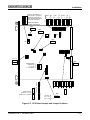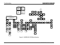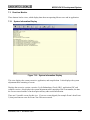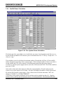
1
Union Switch & Signal Inc., an Ansaldo Signal company
SM-6800J
1000 Technology Drive, Pittsburgh, PA 15219 ● 645 Russell Street, Batesburg, SC 29006
®
MICROLOK II
End Point System
Service Manual
♦ Installation
♦ Maintenance
COPYRIGHT © 2005
UNION SWITCH & SIGNAL
November 2005
Revision 1
SM 6800J, Rev. 1, November 2005
Notices
Proprietary Notice
This document and its contents are the property of Union Switch & Signal Inc.
(hereinafter US&S). This document has been furnished to you on the following
conditions: no right or license under any patents or any other proprietary right in respect
of this document or its content is given or waived in supplying this document. This
document and its contents are not to be used or treated in any manner inconsistent with
the rights of US&S, or to its detriment, and are not to be copied, reproduced, disclosed to
others, or transferred without the prior written consent of US&S.
Important Notice
US&S constantly strives to improve our products and keep our customers apprised of
changes in technology. Following the recommendations contained in the attached service
manual will provide our customers with optimum operational reliability. The data
contained herein purports solely to describe the product, and does not create any
warranties.
Within the scope of the attached manual, it is impossible to take into account every
eventuality that may arise with technical equipment in service. Please consult your local
US&S Account Executive in the event of any irregularities with our product.
We expressly disclaim liability resulting from any improper handling or use of our
equipment, even if these instructions contain no specific indication in this respect. We
strongly recommend that only approved US&S spare parts be used as replacements.
SM 6800J, Rev. 1, November 2005
i
Revision History
Revision History
ii
Rev.
Date
Nature of Revision
Original
February 27, 2004
Original Issue
1
November 2005
Incorporate ECO 140114-1; Eliminate reference to
bipolar inputs
SM 6800J, Rev. 1, November 2005
Table of Contents
TABLE OF CONTENTS
1
INTRODUCTION...........................................................................................................1-1
1.1
Scope ..................................................................................................................................................... 1-1
1.2
RAIL Team and Technical Support ........................................................................................................ 1-2
1.3
References ............................................................................................................................................. 1-2
1.3.1
US&S Supporting Documentation ................................................................................................. 1-2
2
DESCRIPTION..............................................................................................................2-1
2.1
Safety ..................................................................................................................................................... 2-1
2.2
Specifications ......................................................................................................................................... 2-4
2.2.1
Electrical ........................................................................................................................................ 2-4
2.2.2
Mechanical..................................................................................................................................... 2-4
3
SYSTEM COMPONENTS FUNCTIONAL DESCRIPTION ...........................................3-1
3.1
Board Addressing................................................................................................................................... 3-1
3.2
LAMP16 PCB ......................................................................................................................................... 3-2
3.3
Power Supply/Conditional Power Supply (CPS).................................................................................... 3-8
3.4
IN8.OUT8 Mixed Vital I/O PCB ............................................................................................................ 3-10
3.5
CPU ...................................................................................................................................................... 3-14
3.5.1
Serial Communication Link.......................................................................................................... 3-15
3.6
Coded Track I/O ................................................................................................................................... 3-18
3.6.1
ECode Track PCB ....................................................................................................................... 3-18
3.6.2
MICROTRAX Coded Track PCB................................................................................................. 3-22
3.7
VCOR ................................................................................................................................................... 3-26
4
APPLICATION PROGRAMMING .................................................................................4-1
5
INSTALLATION ............................................................................................................5-1
5.1
Cardfile Cabling...................................................................................................................................... 5-1
5.2
Grounding............................................................................................................................................... 5-2
5.3
Lightning Protection................................................................................................................................ 5-2
5.4
Track Leads and Surge Protection ........................................................................................................ 5-3
5.5
Grounding............................................................................................................................................... 5-3
5.6
Track Polarity ......................................................................................................................................... 5-3
5.7
PCB Configuration.................................................................................................................................. 5-8
5.7.1
CPU Configuration......................................................................................................................... 5-8
6
TROUBLESHOOTING ..................................................................................................6-1
6.1
MICROLOK II Board Level Troubleshooting.......................................................................................... 6-1
6.1.1
Isolating the Malfunction................................................................................................................ 6-1
6.1.2
Serial Link Status Indicator............................................................................................................ 6-2
6.1.3
Restoring the System to Normal Operation................................................................................... 6-3
6.2
Troubleshooting an ECode Track Circuit ............................................................................................... 6-5
SM 6800J, Rev. 1, November 2005
iii
Table of contents
7
MICROLOK II DEVELOPMENT SYSTEM ....................................................................7-1
7.1
Main Menu.............................................................................................................................................. 7-2
7.2
Top Toolbar Buttons............................................................................................................................... 7-3
7.2.1
Advanced Button/System Memory Dump ..................................................................................... 7-3
7.2.2
Settings Button/Program Settings ................................................................................................. 7-5
7.2.2.1
View Tab .................................................................................................................................... 7-5
7.2.2.2
Symbol Files Tab........................................................................................................................ 7-6
7.2.2.3
Logic Monitor Tab ...................................................................................................................... 7-7
7.2.2.4
Advanced Tab ............................................................................................................................ 7-8
7.2.3
Split................................................................................................................................................ 7-9
7.3
Run-time Monitor.................................................................................................................................. 7-11
7.3.1
System Information Display......................................................................................................... 7-11
7.3.2
Board Information ........................................................................................................................ 7-12
7.3.3
Free Run Variable Display........................................................................................................... 7-13
7.3.3.1
All Button .................................................................................................................................. 7-14
7.3.3.2
Advanced Button ...................................................................................................................... 7-14
7.3.3.3
Freeze Button........................................................................................................................... 7-14
7.3.3.4
Save Button.............................................................................................................................. 7-14
7.3.4
Dynamic Bit Variable View .......................................................................................................... 7-15
7.3.4.1
All Button .................................................................................................................................. 7-16
7.3.4.2
None Button ............................................................................................................................. 7-16
7.3.4.3
White Text Box ......................................................................................................................... 7-16
7.3.4.4
Advanced Button ...................................................................................................................... 7-16
7.3.4.5
Freeze Button........................................................................................................................... 7-16
7.3.4.6
Clear Button ............................................................................................................................. 7-16
7.3.5
Serial Message Monitor............................................................................................................... 7-17
7.4
Historical Data ...................................................................................................................................... 7-19
7.4.1
User Data Log ............................................................................................................................. 7-19
7.4.1.1
Viewing Raw Data .................................................................................................................... 7-22
7.4.1.2
Saving the Log ......................................................................................................................... 7-22
7.4.2
Save Comma Delimited View ...................................................................................................... 7-23
7.4.3
System Event Log ....................................................................................................................... 7-24
7.4.3.1
Reload Button........................................................................................................................... 7-24
7.4.3.2
Clear Button ............................................................................................................................. 7-25
7.4.3.3
Abort Button ............................................................................................................................. 7-25
7.4.3.4
Displaying Codes ..................................................................................................................... 7-25
7.4.4
System Error Log......................................................................................................................... 7-27
7.4.4.1
Printing the Log ........................................................................................................................ 7-28
7.4.5
Merged Events Log ..................................................................................................................... 7-28
7.5
System Adjustment/Setup .................................................................................................................... 7-29
7.5.1
Set time of Day Clock .................................................................................................................. 7-29
7.5.2
Reset MICROLOK II ........................................................................................................................ 7-30
7.5.3
System Configuration .................................................................................................................. 7-31
7.5.3.1
Configuring the MICROLOK II System ........................................................................................ 7-32
7.5.3.1.1 Overview ............................................................................................................................. 7-32
7.5.3.1.2 Procedure to Access the System Configuration Options ................................................... 7-33
7.5.3.1.3 Configuring The General System Settings ......................................................................... 7-33
iv
SM 6800J, Rev. 1, November 2005
Table of Contents
7.5.3.1.4 Changing Configurable Timers ........................................................................................... 7-34
7.5.3.1.5 To Change a Timer Configuration Value ............................................................................ 7-35
7.5.3.1.6 Changing The User-Defined Variables............................................................................... 7-35
7.5.3.1.7 Changing User Log Selections ........................................................................................... 7-35
7.5.3.1.8 To Set a Parameter for Inclusion in the User Log .............................................................. 7-35
7.5.3.1.9 Enabling, Disabling, and Configuring Printed Circuit Boards ............................................. 7-36
7.5.3.1.10 Changing Serial Link Configurations ................................................................................7-36
7.5.3.2
Completing the Configuration Process .................................................................................... 7-37
7.5.3.2.1 The Done with Configuration and Cancel Configuration Buttons ....................................... 7-37
7.5.4
Software Upload View ................................................................................................................. 7-37
7.5.5
Application Download Screen ..................................................................................................... 7-41
7.6
Offline Tools ......................................................................................................................................... 7-42
7.6.1
Run the Compiler......................................................................................................................... 7-42
7.6.2
Run the Reverse Compiler .......................................................................................................... 7-43
7.6.3
Run the Comparison Tool............................................................................................................ 7-44
7.6.4
Cardfile/Power Calculation .......................................................................................................... 7-45
7.6.5
Event/Error Code Help ................................................................................................................ 7-47
7.7
Close Window/Exit Application............................................................................................................. 7-48
7.7.1
Exiting the Development System................................................................................................. 7-48
SM 6800J, Rev. 1, November 2005
v
Table of contents
LIST OF FIGURES
Figure 2-1. End Point System Cardfile Typical Full Configuration..................................................................... 2-2
Figure 2-2. End Point System Cardfile with Standard Wall-Mount Ears............................................................ 2-5
Figure 3-1. End Point System Motherboard....................................................................................................... 3-1
Figure 3-2. Battery Wiring for Isolated LAMP16 Power ..................................................................................... 3-3
Figure 3-3. Vital LAMP Output PCB Block Diagram .......................................................................................... 3-4
Figure 3-4. Typical LAMP16/VCOR Output Wiring ............................................................................................ 3-4
Figure 3-5. Typical LAMP16 Output Wiring with Fail to Red Indication ............................................................. 3-5
Figure 3-6. LAMP16 PCB Front Panel ............................................................................................................... 3-7
Figure 3-7. Power Supply PCB Front Panel ...................................................................................................... 3-9
Figure 3-8. IN8.OUT8 Vital Output PCB Block Diagram.................................................................................. 3-12
Figure 3-9. IN8.OUT8 PCB Front Panel........................................................................................................... 3-13
Figure 3-10. CPU PCB Front Panel ................................................................................................................. 3-17
Figure 3-11. ECode Track PCB Front Panel.................................................................................................... 3-21
Figure 3-12. Complete Track Transmit and Receive Cycle Waveform (typical).............................................. 3-23
Figure 3-13. MICROTRAX Coded Track PCB Front Panel Track I/O PCB ........................................................ 3-25
Figure 3-14. End Point System Cardfile Standard Internal VCOR Wiring ....................................................... 3-27
Figure 5-1. Coded Track Interface Panels - Typical Basic Track Wiring ........................................................... 5-4
Figure 5-2. End Point System ECode Track Circuit Configuration .................................................................... 5-5
Figure 5-3. End Point System ECODE/MICROTRAX Track Circuit Configuration................................................. 5-6
Figure 5-4. Cardfile Power Input Wiring and Protection .................................................................................... 5-7
Figure 5-5. CPU Board Jumper and Jumper Positions.................................................................................... 5-11
Figure 6-1. MICROLOK II CPU Menu Hierarchy ............................................................................................... 6-4
Figure 7-1. MICROLOK II Development System Icon ........................................................................................... 7-1
Figure 7-2. Dev. System Main Menu.................................................................................................................. 7-2
Figure 7-3. System Memory Dump Screen........................................................................................................ 7-3
Figure 7-4. System Memory Dump View ........................................................................................................... 7-4
Figure 7-5. Program Settings/View Property Tab .............................................................................................. 7-5
Figure 7-6. Program Settings/Symbol Files Property Tab ................................................................................. 7-6
Figure 7-7. Program Settings/Logic Monitor Property Tab ................................................................................ 7-7
Figure 7-8. Program Settings/Advanced Property Tab ...................................................................................... 7-8
Figure 7-9. Split Screens.................................................................................................................................. 7-10
Figure 7-10. System Information Display ......................................................................................................... 7-11
Figure 7-11. Board Information Display ........................................................................................................... 7-12
Figure 7-12. Free Run Display ......................................................................................................................... 7-13
Figure 7-13. Dynamic Bit Variable Display ...................................................................................................... 7-15
vi
SM 6800J, Rev. 1, November 2005
Table of Contents
Figure 7-14. Serial Message Monitor ............................................................................................................... 7-17
Figure 7-15. Program Settings Dialog Box View Tab ...................................................................................... 7-19
Figure 7-16. User Data Log Dialog Box ........................................................................................................... 7-20
Figure 7-17. User Data Log Display................................................................................................................. 7-21
Figure 7-18. Save Comma Delimited View ...................................................................................................... 7-23
Figure 7-19. Event Screen Display .................................................................................................................. 7-24
Figure 7-20. Program Settings Dialog Box ...................................................................................................... 7-25
Figure 7-21. Event Screen with Codes Column............................................................................................... 7-26
Figure 7-22. System Error Log......................................................................................................................... 7-27
Figure 7-23. Merged Event Log ....................................................................................................................... 7-28
Figure 7-24. Set Time of Day Clock Display .................................................................................................... 7-29
Figure 7-25. MICROLOK II Reset Dialog Box...................................................................................................... 7-30
Figure 7-26. System Configuration Dialog Box................................................................................................ 7-31
Figure 7-27. Typical System Configuration Display ......................................................................................... 7-32
Figure 7-28. System Adjustment/Setup Software Upload Display................................................................... 7-37
Figure 7-29. Software Upload File Open Dialog Box ....................................................................................... 7-38
Figure 7-30. Software Upload Invalid File Dialog Box ..................................................................................... 7-39
Figure 7-31. Software Upload Progress Dialog Box ........................................................................................ 7-40
Figure 7-32. Application Download Screen...................................................................................................... 7-41
Figure 7-33. Compiler Dialog Box .................................................................................................................... 7-42
Figure 7-34. Dev. System Reverse Compiler Dialog Box................................................................................ 7-43
Figure 7-35. Dev. System Comparison Tool Dialog Box ................................................................................. 7-44
Figure 7-36. Dev. System Power Calculation .................................................................................................. 7-45
Figure 7-37. Dev. System Event/Error Code Help Screen .............................................................................. 7-47
Figure 7-38. Dev. System Exit Screen ............................................................................................................. 7-48
SM 6800J, Rev. 1, November 2005
vii
Table of contents
LIST OF TABLES
Table 2-1. End Point System Cardfile and Plug-In Components....................................................................... 2-3
Table 3-1. LAMP16 PCB Specifications............................................................................................................. 3-6
Table 3-2. LAMP16 PCB Indications.................................................................................................................. 3-6
Table 3-3. Power Supply PCB Specifications .................................................................................................... 3-8
Table 3-4. Power Supply/CPS Indicators........................................................................................................... 3-8
Table 3-5. IN8.OUT8 PCB Indicators............................................................................................................... 3-10
Table 3-6. Connector Data for IN8.OUT8 PCBs .............................................................................................. 3-11
Table 3-7. IN8.OUT8 Board Specifications...................................................................................................... 3-11
Table 3-8. COM Port #3 J14/J15 Connector Pin-Outs .................................................................................... 3-15
Table 3-9. CPU Controls and Indicators .......................................................................................................... 3-16
Table 3-10. Connector Data for TRACK I/O PCBs .......................................................................................... 3-18
Table 3-11. ECode Track PCB Indicators........................................................................................................ 3-19
Table 3-12. MICROTRAX Track PCB Specifications .......................................................................................... 3-22
Table 3-13. MICROTRAX Coded Track PCB Indicators..................................................................................... 3-24
Table 5-1. CPU Jumpers.................................................................................................................................... 5-8
viii
SM 6800J, Rev. 1, November 2005
Introduction
1
INTRODUCTION
MICROLOK®II End Point System is a simplified MICROLOK II system that has a package style similar to
MICROTRAX® and i-Lok. To eliminate external Input/Output (I/O) cables used in MICROLOK II system
the Printed Circuit Board (PCB) top rear connector now plugs into a motherboard mounted mating
connector. The motherboard carries all wiring from this connector to cage clamp terminals on the top
portion of the motherboard (See Figure 2-1). I/O wires connect directly to these connectors.
Address jumpers for the LAMP16 and Track boards (the I/O board's addresses are preset) are located
on the motherboard. The Electrically Erasable Programmable Read Only Memory (EEPROM) that
stores system configuration is also located on the motherboard.
As in the MICROTRAX and i-Lok®systems, the Vital Cut-Off Relay (VCOR) is housed within the
cardfile eliminating the need for external wiring and shelf or rack space for this relay. The system can
use either a Union Switch & Signal (US&S) or General Railway Signaling (GRS) relay as the VCOR.
Refer to Table 2-1 for cardfile part numbers that correspond to the VCOR relay in use.
The End Point System is for use with a nominal 12VDC supply only.
1.1
Scope
This manual provides the following information on the End Point System:
• System Description
•
Operation
•
Installation
•
Troubleshooting
•
Parts List
MICROLOK®II is a registered trademark of Union Switch and Signal (US&S).
MICROTRAX ® is a registered trademark of Union Switch and Signal (US&S).
i-Lok ® is a registered trademark of Union Switch and Signal (US&S).
SM 6800J, Rev. 1, November 2005
1-1
Introduction
1.2
RAIL Team and Technical Support
The Rapid Action Information Link (RAIL) team was created in
1996 to serve the technical needs of current and potential US&S
customers. Convenient 24-hour access and a rapid resolution to
customer problems are the trademarks of this organization. The
RAIL team, which is staffed primarily by US&S product and
application engineers, is ready to assist and resolve any technical
issues concerning the MICROLOK II system or any other US&S
product.
Any questions regarding the contents of this service manual should
be directed to the RAIL team by telephone at 1-800-652-7276 or
through Internet E-mail at [email protected].
1.3
References
1.3.1 US&S Supporting Documentation
•
US&S MICROLOK II System Description
SM-6800A
•
US&S MICROLOK II Hardware Installation
SM-6800B
•
US&S MICROLOK II System Startup, Troubleshooting,
and Maintenance
SM-6800C
•
US&S MICROLOK II ECode® and i-Lok Addendum
SM-6800E
•
US&S MICROTRAX Coded Track Circuit Service Manual
SM-6470B
•
US&S PN-150B DC Plug-In Relays
SM-4551
ECode® is a registered trademark of Union Switch and Signal (US&S).
1-2
SM 6800J, Rev. 1, November 2005
Description
2
DESCRIPTION
This system design uses existing MICROLOK II Printed Circuit Boards (PCBs). It is used for
MICROTRAX or ECode coded track circuits in applications where a plug-in system with set I/O is
desirable.
The top rear PCB connectors and custom cables (used in MICROLOK II cardfile wiring) are replaced by
the End Point System motherboard. These connections are brought, via the motherboard, to front
accessible WAGO connectors. These plug-in input/output connectors and a VCOR integral to the
cardfile make the unit easier to install and replace. Systems are available for use with either a US&S
or GRS style Vital Cut-Off Relay (VCOR).
The system supports the MICROLOK II software, including the generic system software (executive) and
the Development System (compiler, reverse compiler, comparison tool, and maintenance tool). No
software changes are required for this system.
The intended applications are as an intermediate unit, simple end of siding, and EC4H (ECode – End
of Siding configuration) replacement.
Refer to Figure 2-1 for a complete cardfile configuration.
2.1
Safety
Read and thoroughly understand this manual before attempting any of the procedures listed.
Pay particular attention to:
WARNING
and
CAUTION
statements that appear throughout this manual. Caution statements indicate conditions that could cause
damage to equipment. Warning statements indicate conditions that could cause physical harm, serious
injury, or loss of life. Always observe standard precautions familiar to trained electrical technicians.
Always adhere to all safety regulations stipulated by the railroad.
SM 6800J, Rev. 1, November 2005
2-1
Description
BVCOR2
ON
BVCOR3
8IN.8OUT
BOARD #4
8IN.8OUT
BOARD #3
8IN.8OUT
BOARD #5
TRACK
BOARD #6
COM3
OUT1+
OUT1-
OUT1+
OUT1-
OUT1+
OUT1-
OUT1+
OUT1- OUT1+
OUT1-
2
OUT2+
OUT2-
OUT2+
OUT2-
OUT2+
OUT2-
OUT2+
OUT2- OUT2+
OUT2-
3
OUT3+
OUT3-
OUT3+
OUT3-
OUT3+
OUT3-
OUT3+
OUT3- OUT3+
OUT3-
4
OUT4+
OUT4-
OUT4+
OUT4-
OUT4+
OUT4-
OUT4+
OUT4- OUT4+
OUT4-
B+
5
OUT5+
OUT5-
OUT5+
OUT5-
OUT5+
OUT5-
OUT5+
OUT5- OUT5+
OUT5-
B-
6
OUT6+
OUT6-
OUT6+
OUT6-
OUT6+
OUT6-
OUT6+
OUT6- OUT6+
OUT6-
7
OUT7+
OUT7-
OUT7+
OUT7-
OUT7+
OUT7-
OUT7+
OUT7- OUT7+
OUT7-
8
OUT8+
OUT8-
OUT8+
OUT8-
OUT8+
OUT8-
OUT8+
OUT8- OUT8+
OUT8-
10
IN1+
IN1-
IN1+
IN1-
IN1+
IN1-
IN1+
IN1-
IN1+
IN1-
11
IN2+
IN2-
IN2+
IN2-
IN2+
IN2-
IN2+
IN2-
IN2+
IN2-
A+
12
IN3+
IN3-
IN3+
IN3-
IN3+
IN3-
IN3+
IN3-
IN3+
IN3-
A-
13
IN4+
IN4-
IN4+
IN4-
IN4+
IN4-
IN4+
IN4-
IN4+
IN4-
14
IN5+
IN5-
IN5+
IN5-
IN5+
IN5-
IN5+
IN5-
IN5+
IN5-
B+
15
IN6+
IN6-
IN6+
IN6-
IN6+
IN6-
IN6+
IN6-
IN6+
IN6-
B-
16
IN7+
IN7-
IN7+
IN7-
IN7+
IN7-
IN7+
IN7-
IN7+
IN7-
IN8+
IN8-
IN8+
IN8-
IN8+
IN8-
IN8+
IN8-
IN8+
IN8-
A+
14
1
1
A-
TRACK
BOARD #7
1
5KP
16A
BVCOR4
BVCOR5
13
FUSE
10A
M ICRO LO K II
UNION SWITCH & SIGNAL
1
5V ON
OUT1
OUT1
OUT1
OUT1
OUT1
2
VCOR
OUT2
OUT2
OUT2
OUT2
OUT2
3
OUT3
OUT3
OUT3
OUT3
OUT3
4
OUT4
OUT4
OUT4
OUT4
OUT4
5
OUT5
OUT5
OUT5
OUT5
OUT5
6
OUT6
OUT6
OUT6
OUT6
OUT6
7
OUT7
OUT7
OUT7
OUT7
OUT7
8
OUT8
OUT8
OUT8
OUT8
OUT8
IN1
IN1
IN1
10
IN2
IN2
IN2
IN2
IN2
11
IN3
IN3
IN3
IN3
IN3
XMIT VOLTAGE
1
2
3
4
B
C
D
Code 5
T 3
12
IN4
IN4
IN4
IN4
IN4
IN5
IN5
IN5
IN5
IN5
A
R 7 5M
B
6
14
IN6
IN6
IN6
IN6
IN6
IN7
IN7
IN7
IN7
IN7
L
16
IN8
IN8
IN8
IN8
IN8
M
E
N
U
8
0
2
TRACK SIGNALS
ADJUST
DOWN
ACTION
ACCEPT
X
M
I
T
RECEIVE
VALID MESSAGE
RECEIVED
SLAVE
TRACK B
UP
UP
TRANSMIT
LEVEL ADJUST
STEADY
NORMA
L
OFF
RECEIVER
R
TRANSMITTER
6
4
8
0
2
TRANSMIT
LEVEL ADJUST
STEADY
DOWN
NORMAL
REJECT
OFF
X
M
I
T
TRACK
POWER SUPPLY
LAMP16
+
RECEIVER
TRANSMITTER
15
MASTER
M
M
TRACK A
4
13
RECEIVE
VALID MESSAGE
RECEIVED
R - CODE RECEIVED
T - CODE TRANSM ITTED
7
8
RESET
+
TRACK SIGNALS
DISPLAY ON
CPU BOARD
5
6
VPP ON
IN1
REC CURRENT
XMIT CURRENT
A
PIN 2 - TXD
PIN 3 - RXD
PIN 4 - RTS
PIN 5 - CTS
PIN 7 - REF
PIN 8 - DCD
PIN 15 - TXCLK
PIN 17 - RXCLK
TRACK CODE
US&S
ON LINE
IN1
PUSH TO
SELECT
DISPLAY MODE
0000
E
9
14
9
OFF
BATTERY-
8IN.8OUT
BOARD #2
25
BATTERY+
BVCOR1
POWER
ON
8IN.8OUT
BOARD #1
LAMP
RETURNS
25
LAMP 16
BOARD #8
13
B12
VCOR
RELAY
CONTACTS
IN8
.OUT8
IN8
.OUT8
IN8
.OUT8
IN8
.OUT8
IN8
.OUT8
68332
CPU
ECode TRACK
N4519100701
RS-232
DTE
N170
61301
Figure 2-1. End Point System Cardfile Typical Full Configuration
2-2
SM 6800J, Rev. 1, November 2005
Description
Table 2-1. End Point System Cardfile and Plug-In Components
CARDFILE
SLOT
US&S PART NO.
Cardfile
NA
N18002701
US&S VCOR
Cardfile
NA
N18002801
GRS VCOR
NAME
VCOR
NA
Lamp 16 Board
1
N322500-701
(US&S PN-150B)
relay
BASIC FUNCTIONS
This is a vital relay used to remove battery
power to the outputs, lamp or relay loads,
when a critical fault has been detected.
A62-0125 (GRS
Type B1 Biased
DC, 500 ohm relay
N17060101
Power Supply
PCB
Controls 16 signal lamps in color lights and
searchlight signals.
Regulates and protects external power
input, conditions and converts the battery
input voltage to the various voltage levels
required for cardfile circuitry operation and
energizes the VCOR relay under the control
of the Central Processor Unit (CPU) board.
Standard MICROLOK II Power Supply without
Front Panel: N1660301
N166X0301
2
or
N166X120X
Standard MICROLOK II Power Supply with
Front Panel: N16660301
MICROLOK II Enhanced Power Supply without
Front Panel:
•
N16601201 Power Supply PCB, without
Isolation Power Supply.
•
N16601203 Power Supply PCB, fully
populated.
MICROLOK II Enhanced Power Supply with
Front Panel:
IN8.OUT8
Boards
•
N16661201 Power Supply PCB, without
Isolation Power Supply.
•
N16661203 Power Supply PCB, fully
populated.
Provides same I/O functions as standard
vital output PCB and vital input PCB on one
board.
3–7
N17061601(12V)
For vital output - it controls standard ± vital
outputs (switch machine relay coil or
MICROLOK II isolation module, for example).
For vital input – It receives standard ± vital
inputs.
SM 6800J, Rev. 1, November 2005
2-3
Description
NAME
CARDFILE
SLOT
US&S PART NO.
BASIC FUNCTIONS
N17061301
Provides system vital controlling logic, vital
I/O management, external serial
communications, application logic execution,
internal and external diagnostics, event
logging, and a user programming and
diagnostics interface.
N451910-0701
Provides train detection in mainline
Alternating Current (AC) coded track
circuits. Versions for non-cab applications
and cab applications at various frequencies.
N17063901
Provides train detection in mainline DC
coded track circuits. Versions for non-cab
applications and cab applications at various
frequencies.
CPU PCB
8
Track Boards
(MICROTRAX)
ECode Track
Board
2.2
9/10
9/10
Specifications
2.2.1 Electrical
Input Power
System Battery from 9.8 to 16.2VDC, fuse protected (10A)
(minimum voltage required for system start is 11.2VDC)
Power Connection
Five Association of American Railroads (AAR) Terminals
2.2.2 Mechanical
The-following mechanical specifications are applicable to the End Point System cardfile:
Dimensions
19"W x 16.76"H x 11.09"D
Material
Stainless steel
Weight
@30lbs with a minimum card complement.
Mounting
The cardfile is supplied with wall mounting ears permanently attached to
the cardfile rear. Optional mounting kit Part Number X18000802 is
available for rack (front) mounting or shelf (bottom) mounting is
available in Part Number X180025021.
2-4
SM 6800J, Rev. 1, November 2005
Description
Figure 2-2. End Point System Cardfile with Standard Wall-Mount Ears
(shown without PCBS)
SM 6800J, Rev. 1, November 2005
2-5
Description
2-6
SM 6800J, Rev. 1, November 2005
System Components Functional Description
3
SYSTEM COMPONENTS FUNCTIONAL DESCRIPTION
Detailed descriptions for the MICROLOK II PCBs can be obtained from the MICROLOK II Service
Manuals SM-6800A, B, and C. The following sections will present information unique to the End
Point System concerning these boards.
3.1
Board Addressing
Board addressing is user adjustable for the LAMP16, and the Track I/O boards via jumpers located on
the motherboard next to the respective PCB rear top connectors (See Figure 3-1). The CPU and Power
Supply PCBs do not have addresses. The addressing for the IN8.OUT8 PCBs are set in the
motherboard traces and cannot be modified. They must be entered into the application program as the
first five boards in the system (Refer to Section 4).
J1 J2
J3
J4
J5
J6
J7
J8
J9
J10
J11 J12
J13
J15
J16
AAR
Terminal
Strip
J14
Address
Select
Jumpers
Address
Select
Jumpers
EEPROM
Figure 3-1. End Point System Motherboard
SM 6800J, Rev. 1, November 2005
3-1
System Components Functional Description
3.2
LAMP16 PCB
The End Point System cardfile supports one LAMP16 PCB (Slot #1) for the control of up to 16
aspects. See Table 3-1 for the lamp/wattage specifications for the PCB.
This LAMP16 printed circuit board (part number N17060101) enables the End Point System CPU to
directly operate signal lamps. Configurations are defined using the CPU board front panel switches
and displays, or using the MICROLOK II Maintenance Tools program loaded on a laptop personal
computer. The configuration data is stored in the CPU EEPROM mounted on the motherboard.
Refer to the conceptual block diagram of a vital output shown in Figure 3-3 for the following
discussion.
Outputs from this board are controlled by "low side" software switches, thus lamps must be connected
from the output through a front contact of the VCOR relay to battery (+). A short from an output to
N12 or B12 will not cause damage, but the system will detect an error and shut down due to the false
lighting of a lamp.
Lamp voltage is adjusted using external variable series resistors in the lamp lines for each signal head.
These resistors, typically mounted in the End Point System equipment rack, protect the lamp board
from damage by limiting current in the event of a short circuit outside the equipment house. Voltage
on the lamp boards can be increased to up to 18VDC if required because of long run cables.
Current to the lamps is shared through four of the VCOR contacts. As shown in Figure 3-4 Terminals
1 and 2 of the AAR terminals are wired to J1 through four VCOR front contacts. J1 is the BVCOR
(vital battery) bus where the field wiring is connected (See Figure 3-1). Lamp returns are brought back
to J2 and the motherboard passes the connection to the LAMP16 PCB, which switches the lamp line to
N12.
As shipped from the factory there are three straps provided on the AAR terminal block to distribute
system battery to feed to the lamps (See Figure 3-14). The lamp power can be isolated from the
system power. To drive the aspects with an isolated source (lamp battery), remove the straps between
Terminals 2 and 3 and between 4 and 5 (See Figure 3-2) leave the strap between Terminals 1 and 2.
Connect the positive side of the isolated battery to Terminals 1 and the negative side to Terminal 5.
See Figure 3-5 for typical output wiring illustrating: fail to red indication (lamps 1, 2, and 3), wiring
for one dropping resistor per three aspects (lamps 4, 5, and 6), and one dropping resistor per aspect
(lamp 7, 8, and9).
3-2
SM 6800J, Rev. 1, November 2005
System Components Functional Description
NOTE
The failover to red function necessitates the addition of an external relay
wiring as per Figure 3-5.
Cardfile
AAR Terminal
Strip
No Straps
Term #1
Term #2
LAMP16
Isolated
Battery
Term #3
System
Battery
Term #4
Term #5
To Lamp Battery
Common
Figure 3-2. Battery Wiring for Isolated LAMP16 Power
SM 6800J, Rev. 1, November 2005
3-3
System Components Functional Description
LAMP16 PCB
Power For Lamp
Switching Circuits
Cardfile
Internal
VCOR
Relay
Internal
Cardfile
Wiring
B12
Lamp
Wattage
Adjust
(External)
Lamp Drive
“X”
Low-Side
Switch
N12
CPU
Control
Figure 3-3. Vital LAMP Output PCB Block Diagram
BVCOR
BUS
AAR
TERM #1
AAR
TERM #1
LAMP16
PCB
AAR
TERM #2
AAR
TERM #2
J1
J2
Figure 3-4. Typical LAMP16/VCOR Output Wiring
3-4
SM 6800J, Rev. 1, November 2005
System Components Functional Description
Fail To Red
WAGO TERMINAL STRIPS FOR
THE LAMP16 BOARD. THESE
ARE LOCATED ON THE TOP
LEFT SIDE OF THE CARDFILE
MOTHERBOARD.
VCOR
Contacts
LAMP 16
SLOT #1
BVCOR 1
LAMP
RETURNS
EXTERNAL
VCOR
REPEATER
RELAY
N12
EXTERNALVCOR
REPEATER
RELAY CONTACTS
1
G
2
Y
3
N12
1
4
G
2
3
BVCOR 2
4
5
Y
5
CARDFILE
INTERNAL WIRING
6
BVCOR 3
7
6
R
8
9
10
BVCOR 4
B12
R
7
G
11
12
BVCOR 5
13
8
Y
14
15
16
J1
9
R
J2
Figure 3-5. Typical LAMP16 Output Wiring with Fail to Red Indication
SM 6800J, Rev. 1, November 2005
3-5
System Components Functional Description
Table 3-1. LAMP16 PCB Specifications
US&S
PART
NO.
N17060101
VITAL LAMP OUTPUT PRINTED CIRCUIT BOARDS
SIGNAL
SIGNAL
MAX.
MAX. NO. MAX. NO.
LAMP
LAMP
ACTIVATE
OF 18W
OF 25W
VOLTAGE
WATTAGE
D LOAD
LAMPS
LAMPS
RANGE
RANGE
10V – 12V
300W
16W – 36W
16*
12*
MAX. NO.
OF 36W
LAMPS
8*
*Indicates the total number of lamps that can be on at once for the specified wattage.
Table 3-2. LAMP16 PCB Indications
REFER TO
FIGURE 3-6
LABEL
INDICATOR
PURPOSE
1
1-8
yellow LEDs
Monitors LAMP16 outputs 1 through 8. When lit,
indicates respective lamp output is on.
2
9 - 16
yellow LEDs
Monitors LAMP 16 outputs 9 through 16. When lit,
indicates respective lamp output is on.
Note:
A flashing indicator denotes a burned out signal lamp.
3-6
SM 6800J, Rev. 1, November 2005
System Components Functional Description
1
2
LAMP 16
Figure 3-6. LAMP16 PCB Front Panel
SM 6800J, Rev. 1, November 2005
3-7
System Components Functional Description
3.3
Power Supply/Conditional Power Supply (CPS)
The power supply plugs into Slot #2 of the cardfile and is available in a number of different
configurations dependent on system needs (See Table 2-1).
Table 3-3. Power Supply PCB Specifications
INPUT POWER
9.8 – 16.2VDC
9.8 – 32VDC*
PCB SECTION
Standard Power
Supply
N166X0301
Enhanced Power
Supply
N166X1203
OUTPUT POWER
5VDC at 3 amps
–12VDC at 1 amp
+ 12VDC at 1 amp
5VDC at 5 amps
– 12VDC at 2 amps
+ 12VDC at 1 amp
*End Point System operates only at 12VDC
The Power Supply/CPS board serves a vital role in the fail-safe design of the End Point System.
The power supply board performs these functions:
• Conditional Power Supply (CPS) on the board generates the VCOR voltage (–9VDC to –14VDC)
to energize the VCOR relay in response to the 250Hz signal from the CPU.
•
Produces regulated ±12V and +5V cardfile power from system battery.
Cardfile power is distributed to all system printed circuit boards through the motherboard to the 96-pin
PCB connector.
The +12V output of the power supply board is not used as a source for any vital or non-vital outputs.
External battery power (switched through the VCOR contacts) is used for this purpose.
Current draw on the battery is determined by the application configuration, (number of signal lamps,
cab signal carrier frequency, etc.).
Table 3-4. Power Supply/CPS Indicators
REFER TO
FIGURE 3-7
3-8
LABEL
INDICATOR
PURPOSE
1
5V ON
LED (green)
When lit, indicates 5V operating power on to other
cardfile PCBs.
2
VCOR
LED (green)
When lit, indicates conditional power on to VCOR
relay (CPU diagnostics normal).
SM 6800J, Rev. 1, November 2005
System Components Functional Description
1
2
Figure 3-7. Power Supply PCB Front Panel
SM 6800J, Rev. 1, November 2005
3-9
System Components Functional Description
3.4
IN8.OUT8 Mixed Vital I/O PCB
The mixed vital I/O boards provide up to eight isolated inputs and eight non-isolated outputs. The
eight isolated (+, –) individual vital inputs can be used for inputs such as switch machine
correspondence (bipolar inputs require a relay interface) or OS track circuit occupancy. All eight
negative (–) inputs on the PCB share a common floating N12 (isolated from system ground).
All eight outputs share a common B12. The vital outputs are switched through a software controlled
high-side switch (Refer to Figure 3-8 for a block diagram of the output). The return of this output
(from the relay) must be brought back to the appropriate negative return of the PCB. For example,
output #1 of the PCB in Slot #3 runs from OUT1+ (on J5) to the output relay and then returns to
OUT1– (on J4).
WARNING
DO NOT connect the relay return (–) to some intermediate N12 bus.
Up to five IN8.OUT8 PCBs are supported by the system. They may be plugged into Slots 3 through 7.
Specifications for the mixed vital I/O boards are shown in Table 3-7.
I/O to the PCBs are brought via the motherboard to WAGO connectors located at the top of the
motherboard (See Figure 2-1). See Table 3-6 for connector information.
Table 3-5. IN8.OUT8 PCB Indicators
REFER TO
FIGURE 3-9
LABEL
INDICATOR
1
OUT1 - OUT8
yellow LEDs
Monitor state of vital outputs 1 through 8. When
lit, indicates respective output is turned on.
2
IN1 - IN8
green LEDs
Monitor state of vital inputs 1 through 8. When lit,
indicates respective input is turned on.
3-10
PURPOSE
SM 6800J, Rev. 1, November 2005
System Components Functional Description
Table 3-6. Connector Data for IN8.OUT8 PCBs
DESCRIPTION
WAGO PART NUMBER
COLOR
"J" NUMBERS
J3, 5, 7, 9 and 11 OUT 1-8+/IN1-8+ - Female
Connector, 17 Poles
231-317/037-000
Orange
J709146-1584
J3, 5, 7, 9 and 11 OUT 1-8+/IN1-8+ - Header,
17 Poles
231-347/001-000
Orange
J709146-1585
J4, 6, 8, 10 and 12 OUT 1-8-/IN1-8- - Female
Connector, 17 Poles
231-117/037-000
Gray
J709146-1582
J4, 6, 8, 10 and 12 OUT 1-8-/IN1-8- - Header,
17 Poles
231-147/001-000
Gray
J709146-1583
Coding Fingers
231-129
Gray
J709146-1609
The PCB's lower rear connector uses a keying strip set at the factory per data as shown in Service
Manual SM-6800B.
Table 3-7. IN8.OUT8 Board Specifications
US&S
PART NO.
VOLTAGE
VBATT
RANGE
N17061601
12V
OUTPUT SPECIFICATIONS
LOAD
MAX. OFF
RESISTANCE
VOLTAGE
RANGE
50 Ω - ∞
MIN. ON
VOLTAGE
0.75V
VBATT - 1V
INPUT SPECIFICATIONS
US&S
PART NO.
NOM. INPUT
VOLTAGE
MIN. VOLTAGE
TO
ENSURE ON
STATE
VOLTAGE TO
ENSURE OFF
STATE
MAX.
SUSTAINED
INPUT
VOLTAGE
N17061601
12V
9.5V
7.0V or less
34V
SM 6800J, Rev. 1, November 2005
3-11
System Components Functional Description
Cardfile
Internal
VCOR
Relay
House B12
-
+
OUTconnection on
J4, 6, 8, 10, or 12
IN8.OUT8 PCB (12V)
Internal
Cardfile
Wiring
Controlled
External
Relay
Internal
Cardfile
Wiring
Output
“X”
Polyswitch-Protected
Output “Contact”
High-Side Switch
Analog
Ground
CPU Control
Figure 3-8. IN8.OUT8 Vital Output PCB Block Diagram
3-12
SM 6800J, Rev. 1, November 2005
System Components Functional Description
OUT 1
OUT 2
1
OUT 3
OUT 4
OUT 5
OUT 6
OUT 7
OUT 8
IN 1
IN 2
2
IN 3
IN 4
IN 5
IN 6
IN 7
IN 8
IN8
.OUT8
Figure 3-9. IN8.OUT8 PCB Front Panel
SM 6800J, Rev. 1, November 2005
3-13
System Components Functional Description
3.5
CPU
The CPU board contains the central controlling logic and diagnostic monitoring for the End Point
System. It plugs into Slot 8 of the cardfile.
The CPU performs the following functions:
• Controls power to vital outputs through the cardfile power supply and an external VCOR relay
(fail-safe function).
•
Generates a steady 250Hz check signal that is sent to the power supply board as long as the
diagnostic checks performed continuously by the CPU detect no internal or external system faults.
•
Failure of a diagnostic check results in the removal of the check signal to the power supply board
CPS. This causes the CPS to remove the hold voltage from the VCOR 400Ω relay coil, resulting in
the removal of power to all vital system outputs.
•
Monitors external indications from vital input boards.
•
Processes vital external indications and executing logic defined in the application software.
•
Drives vital output boards as required by the application logic.
•
Monitors and controls the serial communication port (COM 3).
•
Tests individual vital input and output channels for faults (in parallel with control of these
channels) and responds to detected faults.
•
Monitors system internal operation for faults and responds to detected faults.
•
Records system faults and routine events in user-accessible memory.
•
Responding to CPU board front panel switch inputs and operating the associated displays.
•
Interacts with a laptop Personal Computer (PC) during system diagnostic operations, application
logic programming, and executive software upgrading.
•
The executive and application software is stored in four flash EPROMs that provide up to eight
megabytes of memory. Flash EPROMs permit direct handling of the software using a laptop PC
connected to the CPU board front panel serial port connector.
•
Jumpers are provided on the board to lock or unlock the flash EPROMs for programming and to
select the required programming voltage.
•
Two independent banks (128 Kbytes total) of fast static Random Access Memory (RAM) (SRAM)
[Static Random Access Memory] are provided on the CPU board for processing vital data. Events
and errors are stored in up to four 256 Kbyte banks of low power SRAM. Error/event memory is
maintained by a capacitor backup that provides up to four hours of short-term RAM protection.
•
The CPU is also designed to store RAM-type data in one or two Personal Computer Memory Card
International Assoc. (PCMCIA) cards, using a board-mounted cardholder.
•
Two alphanumeric displays on the CPU board provide menus allowing the display of information
without having to connect a laptop PC. The two menus are the Reset and On-Line menus.
3-14
SM 6800J, Rev. 1, November 2005
System Components Functional Description
3.5.1 Serial Communication Link
The End Point System uses only one communications link that can be daisy-chained to other units.
COM port #3 of the PCB connects via the motherboard to two, parallel-wired, 25-pin "D" male
connectors (J13 and J14) located at the top right area of the motherboard (See Figure 2-1). The port
can be used as an RS-232/423 communications link. See Table 5-1 for CPU jumper positioning to
select serial protocol.
Table 3-8. COM Port #3 J14/J15 Connector Pin-Outs
PIN NUMBER
SIGNAL
2
TXD (Transmit Data)
3
RXD (Receive Data)
4
RTS (Request to Send)
5
CTS (Clear To Send)
7
SYSTEM COMMON (N12)
8
DCD (Data Carrier Detect)
15
TXCLK (Transmit Clock)
17
RXCLK (Receive Clock)
SM 6800J, Rev. 1, November 2005
3-15
System Components Functional Description
Table 3-9. CPU Controls and Indicators
REFER TO
FIGURE
3-10
LABEL
DEVICE OR
INDICATOR
PURPOSE
(none)
4-character alphanumeric displays
On-site configuration programming
menus and options.
3
A, B, C, D, E
yellow LEDs
Reserved for serial link status.
4
1, 2, 3, 4, 5, 6, 7, 8
red LEDs
User-defined in application software.
5
ON LINE
green LED
When lit, indicates normal system
operation (successful diagnostics).
1, 2
VPP ON
6
(Voltage Input
Flash
Programming)
yellow LED
When lit, indicates FLASH +5V or +12V
programming voltage enabled (via
board jumper).
7
RESET
green LED
When lit, indicates that the system is in
reset mode.
8
RESET
Momentary
pushbutton
When pressed, resets the CPU. Also
used to place the CPU in the reset
mode.
9
MENU L-R
3-position (return-tocenter) toggle switch
Used to search main program menu
items shown on displays.
10
MENU UP-DOWN
3-position (return-tocenter) toggle switch
Used to select main program menu
items shown on displays.
11
ADJUST UPDOWN
3-position (return-tocenter) toggle switch
Used to cycle through configuration
values shown on displays.
12
ACTION ACCEPTREJECT
3-position (return-tocenter) toggle switch
Executes or cancels menu items shown
on displays.
9-pin connector
Diagnostic link for connection to PC.
RS-232 DTE
13
3-16
(Data Terminal
Equipment)
SM 6800J, Rev. 1, November 2005
System Components Functional Description
1
2
3
4
5
6
7
8
9
10
11
UP
12
13
Figure 3-10. CPU PCB Front Panel
SM 6800J, Rev. 1, November 2005
3-17
System Components Functional Description
3.6
Coded Track I/O
The End Point System cardfile supports two Track I/O boards. Dependent on the application
MICROTRAX (N451910-0701) or ECode (N17063901) track boards can be used in any combination in
Slots 9 and 10 to provide the track circuits interface.
WAGO style connectors (J15 and J16 – See Figure 3-1) are used for the I/O connections. They are
cage clamp termination, plug coupled with finger latches and coding keying fingers. See Table 3-10
for connector information.
Table 3-10. Connector Data for TRACK I/O PCBs
DESCRIPTION
WAGO PART NUMBER
COLOR
"J" NUMBERS
J15 - Female Connector, 5 Poles
231-305/037-000
Orange
J709146-1588
J15 - Header, 5 Poles
231-335/001-000
Orange
J709146-1589
J16 - Female Connector, 5 Poles
721-105/037-000
Light Gray
J709146-1620
J16 - Header, 5 Poles
721-135/001-000
Light Gray
J709146-1621
Coding Fingers
231-129
Gray
J709146-1609
3.6.1 ECode Track PCB
The ECode track interface panel carries all coded track communications between the MICROLOK II
system cardfile and the rails. The circuitry associated with the interface panel minimizes interference
from other signals on the rails. The US&S part number for the ECode track interface panel is
N17600101.
Panel components include a series connected inductor, a replaceable surge protection board with 6.0
volt transzorbs, two fuses, and a series 0.25 ohm resistor that can be shorted out. These components
are mounted on a 1/8 inch thick printed circuit board that is made to be rack mounted. External wiring
to the track is made using 2-way AAR terminal blocks. Wiring to the cardfile is made through a 7-way
plug connector with cage clamp technology.
For cab signal applications, a 10 mH inductor (J702288) must be wired in series with the positive track
terminal of the track interface panel. This will block the 100Hz cab signal from entering the ECode
receiver.
The ECode coded track circuit option is compatible with all versions of Electro Code®. ECode
consists of two elements: a track PCB and a track interface panel. The ECode Track PCB interfaces
with the End Point' System's CPU, where the functions of track messaging and train detection are
performed. Both the track PCB and the interface panel are dual units to handle two independent track
circuits. The interface panel is designed for compatibility with highway crossing audio overlay
Electro Code ® Electro Code 4 ® (EC4) and Electro Code 5 ® (EC5) are registered trademarks of GE
Transportation Systems Global Signaling.
3-18
SM 6800J, Rev. 1, November 2005
System Components Functional Description
equipment and provides secondary surge protection. It is functionally and mechanically equivalent to
the Electro Code 5® (EC5) track interface panel – TIP-2. ECode operates at a fixed receiver sensitivity
of 0.5 amperes and circuits are adjusted at the transmitter via 10 selected output voltages ranging from
1.0 to 2.5 volts.
The ECode Track PCB is linked to both the CPU board and the track interface panel. The CPU
extracts information from the ECode Track PCB to determine track occupancy and track messages.
The interface panel terminates on the track and is also connected to the ECode Track PCB.
ECode is compatible with the Electro Code® family of products.
Configuration details for the ECode Track board can be found in Service Manual SM-6800E.
Table 3-11. ECode Track PCB Indicators
REFER TO
FIGURE 3-11
DEVICE OR
INDICATOR
LABEL
PUSH TO SELECT
DISPLAY MODE
Momentary
pushbutton
switch
1
PURPOSE
Push once to display the transmitted and received
codes for tracks A and B.
Push twice to display the Received Current.
Push three times to display the Transmit Voltage.
Push four times to display the Transmit Current.
Push five times to return to the scrolling menu.
TRACK CODE
red LED
When lit, the transmitted and received codes will be
displayed on the CPU board.
REC CURRENT
red LED
When lit, the receiver current will be displayed on the
CPU board. Range from 0.0 to 3.6 amps in 0.1 amp
increments.
XMIT VOLTAGE
red LED
When lit, the transmit voltage will be displayed on the
CPU board. Range from 1.0 to 2.5 volts, dependent on
rotary switch position.
XMIT CURRENT
red LED
When lit, the transmit current will be displayed on the
CPU board. Range from 0.0 to 6.0 amps in 0.1 amp
increments.
3
TRACK A,
RECEIVER
green LED
When lit, indicates that the received current is greater
than 0.5 amps. Flashing LED represents the received
code.
4
TRACK A,
TRANSMITTER
red LED
When lit, indicates that the transmitter is turned on and
applying a DC signal to the track. Flashing LED
represents the transmitted code.
TRACK A
TRANSMIT LEVEL
ADJUST
10 position rotary
switch
Sets the transmitter output voltage, dependent on track
circuit length. Refer to adjustment table.
2
5
SM 6800J, Rev. 1, November 2005
3-19
System Components Functional Description
REFER TO
FIGURE 3-11
LABEL
TRACK A
XMIT switch
DEVICE OR
INDICATOR
Three-position
toggle switch
PURPOSE
NORMAL position: Board configured for normal track
circuit operation.
STEADY position: Steady DC energy applied to Track A
at a level of 1.0 volt for troubleshooting.
6
OFF position: Transmitter A is turned off and receiver A
is turned on steady for troubleshooting.
7
8
9
green LED
When lit, indicates that the received current is greater
than 0.5 amps. Flashing LED represents the received
code.
red LED
When lit, indicates that the transmitter is turned on and
applying a DC signal to the track. Flashing LED
represents the transmitted code.
TRACK B
TRANSMIT LEVEL
ADJUST
10-position rotary
switch
Sets the transmitter output voltage, dependent on track
circuit length. Refer to adjustment table.
TRACK B
Three-position
toggle switch
NORMAL position: Board configured for normal track
circuit operation.
TRACK B
RECEIVER
TRACK B
TRANSMITTER
XMIT switch
10
STEADY position: Steady DC energy applied to Track B
at a level of 1.0 volt for troubleshooting.
OFF position: Transmitter B is turned off and receiver B
is turned on steady for troubleshooting.
3-20
SM 6800J, Rev. 1, November 2005
System Components Functional Description
1
PUSH BUTTON SWITCH
PUSH TO
SELECT
DISPLAY MODE
2
RED LEDs
TRACK CODE
REC. CURRENT
XMIT VOLTAGE
XMIT CURRENT
TYPICAL CPU BOARD
DISPLAY OF A
TRANSMITTED CODE
AND A RECEIVED CODE
3
GREEN LED
4
5
RED LED
ROTARY SWITCH
(10 POSITION)
6
7
8
9
DISPLAY ON
CPU BOARD
R = CODE RECEIVED
T = CODE TRANSMITTED
CODE 5
M
A
R 7 5M
B
T 3
TRACK A
RECEIVER
TRANSMITTER
6
8
0
4
2
NORMAL
OFF
RECEIVER
RED LED
(3 POSITION)
X
M
I
T
TRACK B
GREEN LED
10 TOGGLE SWITCH
TRANSMIT
LEVEL ADJUST
STEADY
TOGGLE SWITCH
(3 POSITION)
ROTARY SWITCH
(10 POSITION)
M
TRANSMITTER
6
8
0
4
2
TRANSMIT
LEVEL ADJUST
X
M
NORMAL I
T
OFF
STEADY
ECode TRACK
Figure 3-11. ECode Track PCB Front Panel
SM 6800J, Rev. 1, November 2005
3-21
System Components Functional Description
3.6.2 MICROTRAX Coded Track PCB
The coded track circuit PCBs interface the MICROLOK II system to the mainline coded track circuits
(with and without cab signals). The specifications for these boards are as follows:
Table 3-12. MICROTRAX Track PCB Specifications
US&S PART NO.
TRACK CIRCUIT APPLICATION
TRACK CIRCUIT
OPERATING
POWER
N451910-0701
General non-cab and 100Hz cab
signal
9.8 to 16.2VDC
N451910-7601
Required for 40Hz cab signal
9.8 to 16.2VDC
N451910-7602
Required for 50Hz cab signal
9.8 to 16.2VDC
N451910-7603
Required for 60Hz cab signal
9.8 to 16.2VDC
The MICROTRAX Track board is used to manage track circuits by providing end to end rail integrity,
including detection of train shunt, faulty insulated joints, or broken rail. Generally, the track coding
(equivalent to four-wire Home/Distant (HD) circuitry) is accomplished through the rails; however, it
may also operate over line wire.
The track code signal format is AC and is connected to the rails through a Track Interface Panel
consisting of a transformer and a low impedance inductor. The MICROTRAX track code is bipolar,
consisting of a pattern of positive and negative pulses. Each contains an equal number of short
positive and short negative pulses, and an equal number of long positive and long negative pulses. The
master sends a message very six seconds. The code message begins and ends with a 167 msec. guard
pulse and consists of pulses either 167 msec. or 333 msec. in duration with an amplitude of 2Vp-p.
This code format allows for twenty-three possible codes of which twenty-two codes are available for
user applications.
Two of the user codes are intended for non-vital purposes, such as train occupancy or tumble down.
Twenty of the user codes are vital and are available for any purpose. The remaining reserved code is
used to establish communication, referred to as Link-Up.
3-22
SM 6800J, Rev. 1, November 2005
System Components Functional Description
Figure 3-12. Complete Track Transmit and Receive Cycle Waveform (typical)
The coded track circuit is based upon a "handshake" type superiority protocol and the overall system
track coding format must be designed for this feature. The track interface module mounted in the
MICROTRAX unit is capable of operating one "master" and one "slave" portion of two separate track
circuits. On the MICROTRAX Track board, track connections are designated "Master" and "Slave" and
"+" and "–." Either side of the insulated rail joints can be designated Master or Slave; however, after
one end of a track circuit is designated Master or Slave, the other end must be given the opposite
designation.
When establishing rail polarities, two rules must be observed:
• Polarity must be staggered or alternated across a set of insulated joints. For example, if the north
rail is positive on the left side of the joints, the north rail must be negative on the right side of the
joints.
•
The rail must have the same polarity at both ends of the same circuit.
Because the coding format is low frequency AC, track circuit lengths in the range of 22,000 feet @
3 ohms ballast/1000 feet can be attained.
The track code signal connects to the rails through a Track Interface Panel consisting of a transformer
and a low impedance inductor. There are four different types of single-track interface panels that
provide inductance levels ranging from 10 to 40 mH. The 10 mH panel offers about 10 ohms
impedance at 150Hz and proportionately more impedance at higher frequencies. This makes the
MICROTRAX system compatible with highway crossing motion and predictor equipment without need
of external blocking units. The 15 mH Track Interface Panel is designed for maximum compatibility
with 86Hz crossing predictors and should be used where there is 60Hz noise interference.
SM 6800J, Rev. 1, November 2005
3-23
System Components Functional Description
NOTE
Do not use wide-band joint couplers and do not use wide-band shunts as
joint couplers.
For areas where there is 60Hz interference, a Termination Capacitor Printed Circuit Board
(N16401801) may be mounted on the interface panel and is connected across the "line" terminals of
the unit for filtering purposes.
Refer to Service Manual SM-6470B for maintenance and monitoring procedures.
Table 3-13. MICROTRAX Coded Track PCB Indicators
REFER TO
FIGURE 3-13
1
LABEL
TRACK SIGNALS
+
INDICATOR
red LED
2
3
4
(MASTER)
RECEIVE
(MASTER)
VALID MESSAGE
RECEIVED
red LED
5
red LED
6
7
8
(SLAVE)
RECEIVE
(SLAVE)
VALID MESSAGE
RECEIVED
(SLAVE)
3-24
When lit, indicates code received from Slave end
of track circuit.
When dark, indicates code transmission to Slave
end of track circuit.
When lit, indicates valid message received from
Slave end of track circuit.
red LED
red LED
When dark, indicates Master end track circuit
message not accepted (track circuit shunted or in
remove-shunt mode).
When flashing, indicates Slave track circuit "+"
code pulse (alternating with − LED).
When dark, no Slave track circuit activity.
(SLAVE)
TRACK SIGNALS −
When flashing, indicates Master track circuit "-"
code pulse (alternating with + LED).
When dark, no Master track circuit activity.
(MASTER)
TRACK SIGNALS
+
When flashing, indicates Master track circuit "+"
code pulse (alternating with − LED).
When dark, no Master track circuit activity.
(MASTER)
TRACK SIGNALS −
PURPOSE
red LED
When flashing, indicates Slave track circuit "-"
code pulse (alternating with + LED).
When dark, no Slave track circuit activity.
red LED
When lit, indicates code received from Master
end of track circuit.
When dark, indicates code transmission to
Master end of track circuit.
When lit, indicates valid message received from
Master end of track circuit.
red LED
When dark, indicates Slave end track circuit
message not accepted (track circuit shunted or in
remove-shunt mode).
SM 6800J, Rev. 1, November 2005
System Components Functional Description
1
2
3
4
+
TRACK SIGNALS
RECEIVE
VALID MESSAGE
RECEIVED
MASTER
5
6
7
8
+
TRACK SIGNALS
RECEIVE
VALID MESSAGE
RECEIVED
SLAVE
TRACK
N4519100701
Figure 3-13. MICROTRAX Coded Track PCB Front Panel Track I/O PCB
SM 6800J, Rev. 1, November 2005
3-25
System Components Functional Description
3.7
VCOR
The Vital Cut-Off Relay (VCOR) is used by the End Point System to control power to all vital outputs
(See Figure 3-14). The CPU board controls this fail-safe function. The CPU sends a steady 250Hz
check signal to the CPS (on the Power Supply PCB), which uses it to generate the power for the relay
coil. Under this control of the CPU board the VCOR switches power to all cardfile vital output
circuits. The US&S PN-150B vital biased relay incorporates a 400 ohm coil, and 6FB contacts
consisting of low voltage silver-to-silver fronts and silver-to-silver backs.
Either a US&S PN-150B relay (part number N322500-701) or a GRS A62-0125 relay may be used as
the system VCOR. The cardfile part number is determined by the VCOR chosen for the system (See
Table 2-1).
For a detailed description and information concerning the US&S VCOR see the US&S Relay Manual
SM-4551.
3-26
SM 6800J, Rev. 1, November 2005
System Components Functional Description
Cardfile
AAR Terminal
Strip
Cardfile VCOR
Relay Contacts
To J1 pins # 1 & 2
BVCOR 1
Term #1
NC
Term #2
Strap
NC
Term #3
System
Battery
NC
Term #4
NC
Strap
Term #5
To J1 pins # 4 & 5
BVCOR 2
To J1 pins # 7 & 8
BVCOR 3
To J1 pins # 10 & 11
BVCOR 4
To J1 pins # 13 & 14
BVCOR 5
To Vital Output B12
NC
To J1 pins # 14, 15, &16
N12
N12
To System B12
Power
Supply
PCB
Figure 3-14. End Point System Cardfile Standard Internal VCOR Wiring
SM 6800J, Rev. 1, November 2005
3-27
System Components Functional Description
3-28
SM 6800J, Rev. 1, November 2005
Application Programming
4
APPLICATION PROGRAMMING
Application programming for the End Point System is identical to the process used in writing
MICROLOK II applications. Refer to Service Manual SM-6800D for a detailed discussion of application
programming techniques.
The following is an example of an End Point System application program. The IN8.OUT8 PCBs are
listed first in the application even if they are not used (marked as SPARE).
MICROLOK_II PROGRAM END_POINT_EXAMPLE;
INTERFACE
/* This is an example program to illustrate how to structure a program for the End Point System
cardfile */
LOCAL
BOARD: BOARD.1
FIXED ENABLE: 1
TYPE: IN8.OUT8
/* This board is the only vital in8.out8 used in this program
it must be installed in the slot for board 1 */
OUTPUT:
A.REC.D,
B.REC.D,
A.REC.1,
B.REC.1,
SPARE,
SPARE,
SPARE,
SPARE;
INPUT:
A.SEND.D,
B.SEND.D,
A.SEND.1,
B.SEND.1,
SPARE,
SPARE,
SPARE,
SPARE;
BOARD: BOARD.2
FIXED ENABLE: 0 /* This board is defined to ensure the compiler reserves this address
for this board The End Point System cardfile can only use an in8.out8 at
this address. FIXED ENABLE: 0 Defines the board and prevents it's
use*/
TYPE: IN8.OUT8
OUTPUT:
SPARE;
INPUT:
SPARE;
BOARD: BOARD.3
FIXED ENABLE: 0 /* This board is defined to ensure the compiler reserves this address
for this board. The End Point System cardfile can only use an in8.out8 at
this address. FIXED ENABLE: 0 Defines the board and prevents it's
SM 6800J, Rev. 1, November 2005
4-1
Application Programming
TYPE: IN8.OUT8
use*/
OUTPUT:
SPARE;
INPUT:
SPARE;
BOARD: BOARD.4
FIXED ENABLE: 0 /* This board is defined to ensure the compiler reserves this address
for this board. The End Point System cardfile can only use an in8.out8 at
this address. FIXED ENABLE: 0 Defines the board and prevents it's
use*/
TYPE: IN8.OUT8
OUTPUT:
SPARE;
INPUT:
SPARE;
BOARD: BOARD.5
FIXED ENABLE: 0 /* This board is defined to ensure the compiler reserves this address
for this board. The End Point System cardfile can only use an in8.out8 at
this address. FIXED ENABLE: 0 Defines the board and prevents it's
use*/
TYPE: IN8.OUT8
OUTPUT:
SPARE;
INPUT:
SPARE;
BOARD: BOARD.6.DEF.1
ADJUSTABLE ENABLE: 0 /* The user can change the track board address jumpers, so you can
define multiple boards for the same slot. Note that the user
will only be able to use one of the definitions for each slot.
If the final installation uses this board. The user will enable
this definition. ADJUSTABLE ENABLE: 0 makes the board disabled
by default, but this user is allowed to enable the board */
TYPE: ECODE.TRACK
TRACKA:
TRACK.NAME: TRACK_A
ADJUSTABLE ENABLE: 0;
ADJUSTABLE CODE5.SUPPORT: STANDARD;
ADJUSTABLE CODEM.SUPPORT.ENABLED: 0;
FIXED CODE.GROUP.SELECT: FREIGHT;
TRACKB:
TRACK.NAME: TRACK_B
ADJUSTABLE ENABLE: 0;
ADJUSTABLE CODE5.SUPPORT: STANDARD;
ADJUSTABLE CODEM.SUPPORT.ENABLED: 0;
FIXED CODE.GROUP.SELECT: FREIGHT;
BOARD: BOARD.6.DEF.2
ADJUSTABLE ENABLE: 0 /* The user can change the track board address jumpers, so you can
define multiple boards for the same slot. Note that the user
4-2
SM 6800J, Rev. 1, November 2005
Application Programming
will only be able to use one of the definitions for each slot.
If the final installation uses this board. The user will enable
this definition. ADJUSTABLE ENABLE: 0 makes the board disabled
by default, but this user is allowed to enable the board */
TYPE: TRX.TRACK
TRACKA: TKA.ADJ
TRACK.NAME: TKA
OUTPUT:
A.OUT.D;
INPUT:
A.IN.D;
ADJUSTABLE LENGTH: 6;
ADJUSTABLE ENABLE: 1;
TRACKB: TKB.ADJ
TRACK.NAME: TKB
OUTPUT:
B.OUT.D;
INPUT:
B.IN.D;
ADJUSTABLE LENGTH: 6;
ADJUSTABLE ENABLE: 1;
BOARD: BOARD.8.DEF.1
FIXED ENABLE: 0 /* The user can change the lamp board address jumpers, so you can
define multiple boards for the same slot. Note that the user
will only be able to use one of the definitions for this slot.
If the final installation uses this board. The user will enable
this definition. ADJUSTABLE ENABLE: 0 makes the board disabled
by default, but this user is allowed to enable the board */
TYPE: LAMP16
FIXED 18 WATT MODE 0
OUTPUT:
WARE;
LAMP.OUT:
WARE_LO;
BOARD: BOARD.8.DEF.2
FIXED ENABLE: 0 /* The user can change the lamp board address jumpers, so you can
define multiple boards for the same slot. Note that the user
will only be able to use one of the definitions for this slot.
If the final installation uses this board. The user will enable
this definition. ADJUSTABLE ENABLE: 0 makes the board disabled
by default, but this user is allowed to enable the board */
TYPE: LAMP16
FIXED 18 WATT MODE 0
OUTPUT:
EARE;
LAMP.OUT:
EARE_LO;
BOOLEAN BITS
WARELOR,
EARELOR;
SM 6800J, Rev. 1, November 2005
4-3
Application Programming
CONSTANTS
BOOLEAN
TRUE = 1;
LOGIC BEGIN
ASSIGN TRUE TO CPS.ENABLE;
/* THE FOLLOWING TWO LINES BUILD LOR RELAYS FOR LIGHT OUT LOGIC
BY USING THE WARELOR OR EARELOR IN THE LIGHT OUT DOWNGRADE EQUATIONS
YOU CAN ENSURE PROPER BEHAVIOR WHEN A BOARD IS REMOVED */
ASSIGN ~WARE_LO * BOARD.8.DEF.1.ENABLED * CPS.STATUS TO WARELOR;
ASSIGN ~EARE_LO * BOARD.8.DEF.2.ENABLED * CPS.STATUS TO EARELOR;
/* THE FOLLOWING WILL SEND A 'D' CODE IF THE MICROTRAX BOARD IS INSTALLED IN THE SYSTEM
IF THE BOARD IS NOT INSTALLED, NO ERROR WILL OCCUR IF A.SEND.D OR B.SEND.D ARE SET (TRUE)*/
ASSIGN A.SEND.D TO A.OUT.D;
ASSIGN B.SEND.D TO B.OUT.D;
/* THE FOLLOWING WILL SEND A CODE 1 IF THE ECODE BOARD IS INSTALLED IN THE SYSTEM
IF THE BOARD IS NOT INSTALLED, NO ERROR WILL OCCUR IF A.SEND.1 OR B.SEND.1 ARE SET (TRUE)*/
ASSIGN A.SEND.1 TO BOARD.6.DEF.1.TRACK_A.CODE.1.OUT;
ASSIGN B.SEND.1 TO BOARD.6.DEF.1.TRACK_B.CODE.1.OUT;
/* THE FOLLOWING LINES WILL TURN ON WARE OR EARE IF THE PROPER BOARDS ARE INSTALLED
AND THE LAMP IS GOOD.
IF EITHER BOARD IS NOT INSTALLED, NO ERROR WILL OCCUR IF WARE OR EARE ARE SET (TRUE) */
ASSIGN (A.IN.D + BOARD.6.DEF.1.TRACK_A.CODE.1.IN) * WARELOR TO WARE;
ASSIGN (B.IN.D + BOARD.6.DEF.1.TRACK_B.CODE.1.IN) * EARELOR TO EARE;
END LOGIC
END PROGRAM
4-4
SM 6800J, Rev. 1, November 2005
Installation
5
INSTALLATION
Chapter 3 in Service Manual SM-6800B describes the installation of MICROLOK II system peripheral
devices. These practices apply to the End Point System as well.
Detailed information on the installation of the ECode coded track circuit and its associated interface
panel is described in Chapter 2 of Service Manual SM-6800E
Refer to Service Manual SM-6800E for maintenance and monitoring procedures.
MICROTRAX Installation information can be found in Service Manual SM-6470B.
5.1
Cardfile Cabling
US&S recommends the use of twisted pair wiring (two to three turns per foot) for all relay loads to
minimize possible noise. This should be done wherever possible on all I/O wiring.
US&S recommends the physical separation of clean and dirty wiring.
Cables and wires in general should be kept as short as possible to minimize induced line noise.
Battery leads should be as short as possible to minimize voltage drop. They also must be isolated as
much as possible from noisy wiring.
Relay snubs are intended to dissipate large electromagnetic surges from the coil inductance and to
prevent these surges from interfering with normal operation of the End Point System.
US&S recommends that all relays driven by the End Point System be snubbed to prevent unwanted
monitor errors. This is particularly true where the coil load to the End Point System relay driver is
being broken by a series contact.
Relay snubs can also be installed on other relays that are not directly controlled by the End Point
System outputs, but may be contributing to possible noise due to their close proximity to the cardfile
wiring.
US&S recommends the use of TransZorbs (J792736-0002) for relay snubbing. They will have
minimal effect on relay timing.
Follow these wiring practices:
• All output wires should be gathered into a bundle.
•
Input wires should be gathered into a bundle.
•
Power wiring should be gathered into a bundle.
•
Each of these bundles should be physically separated from each other (6" preferred) and all
bundles physically separated from other house wiring.
•
It is particularly important to maintain this physical separation from high-current "dirty" wiring.
SM 6800J, Rev. 1, November 2005
5-1
Installation
When wiring a vital input PCB through a relay contact circuit contained in the same house as the End
Point System cardfile, the signal battery may be used as the energy source to activate the inputs.
Terminals designated (-) may be connected to battery N12 and B12 switched over relay contacts.
5.2
Grounding
All End Point System circuitry is isolated from the End Point System cardfile chassis. This allows the
cardfile to be connected to earth ground for shielding purposes if desired.
5.3
Lightning Protection
In geographic areas where the incidence of lightning is moderate to high, the following external
lightning protection is recommended.
The physical location of the protection devices should be at the Main Terminal Board.
External wiring should be protected with an equalizer lightning arrester from line-to-line (US&S part
number N451552-0101) and with high voltage arresters from line-to-ground (US&S part number
N451552-0201) on each wire pair (See Figure 5-1).
For lamp signal lines the recommended protection device is a Clare/Remtech CG2-145L (US&S part
number J7927360131). This is a two-wire device with no polarity concerns. One of these devices
should be applied to all signal head lines, and wired between each signal line (B12 or N12) and earth
ground.
Typically theses arresters are mounted on the entrance rack of the house for the lamp return lines
When the gas arresters are installed, one side of every arrester will be grounded. The arresters should
be grouped so that they all share a solid grounding bus. This bus must be connected to the earth
ground using the shortest, most direct path possible (no wire bends if possible). It is recommended
that two #6 American Wire Gauge (AWG) conductors be used to make the connection from the
grounding bus to earth ground.
5-2
SM 6800J, Rev. 1, November 2005
Installation
5.4
Track Leads and Surge Protection
Refer to Figure 5-1. Per standard railroad practice, leads from the coded track interface panel should
be equipped with line-to-line and line-to-ground lightning arresters. Special track surge protection or
common mode filtering is not required on these leads.
CAUTION
The track leads to the End Point System coded track interface panel must
be equipped with US&S-specified lightning arresters. Damage to the
End Point System equipment may result from lightning surges if the
arresters are not properly installed.
5.5
Grounding
Chassis grounds are not required for the coded track interface panels.
5.6
Track Polarity
Figure 5-1 shows interconnections between the coded track interface panels and the rails so that proper
polarity is established between adjacent track circuit blocks. Note in the figure that the polarity of the
panel terminals (L+, L-, T+, T-) is reversed from one end of the panel to the other. To confirm the
proper track circuit polarity, use the procedure in Service Manual SM-6800C. It also provides
procedures for all coded track circuit adjustments that must be made during system startup. Figure 5-2
and Figure 5-3 show typical track circuit configurations for the End Point System.
CAUTION
Track polarity between adjacent tracks must be reversed to prevent an
End Point System from communicating through a faulty insulated joint
connection.
NOTE
The wiring between the Track Board and the Track Interface Panel must
be a twisted pair with 3-4 twists per foot. This twisted pair must then be
separated from any "dirty" wiring (i.e., relay and relay control wiring) by
at least 6 inches.
SM 6800J, Rev. 1, November 2005
5-3
Installation
-
+
+
Insulated
Joints
Insulated
Joints
-
+
Insulated
+ Joints
2
2
1
T-
Insulated
Joints -
2
2
2
2
1
T+
L-
2
2
1
1
T-
T+
T-
T+
L+
L-
L+
L-
Coded
Track
Interface
Panels
Coded
Track
Interface
Panels
L+
-
1
T-
T+
L+
L-
1
End Point
Cardfile
1
Twisted pair (3-4 twists per foot)
and separated from "dirty"
wiring (i.e., relay and relay
control) by at least 6 inches.
Coded Track
Circuit PCBs
To
Battery
To End Point
Vital Input PCB
B+
+
-
Quick
Shunt
Module
B-
+
3
4
Out 1
-
+
7
8
Battery
Track 1
2
1
Track 2
Track 2
REC. XMT. REC. XMT.
1
To
Track
5
6
Out 2
Track 1
REC. XMT. REC. XMT.
2
To End Point
Vital Input PCB
7
4
8
5
To
Track
Line-to-Line Arrester
USGA Blue
N451552-0101
2
Line-to-Ground Arrester
USGA Red
N451552-0201
To
Track
T-
T+
T-
T+
L+
L-
L+
L-
To End Point
Cardfile
(See Above)
1
To End Point
Cardfile
(See Above)
Figure 5-1. Coded Track Interface Panels - Typical Basic Track Wiring
5-4
SM 6800J, Rev. 1, November 2005
Installation
Coded Track
“C”
Coded Track
“A”
Coded Track
“B”
A
A
B
B
A
1
A
1
A
B
A
ECODE
INTERFACE
PANEL
B
ECODE
INTERFACE
PANEL
ECode Track
Interface
N17600101
Panel #1
ECode Track
Interface
N17600101
Panel #2
End Point System
Cardfile
BVCOR2
ON
BVCOR3
8IN.8OUT
BOARD #5
TRACK
BOARD #6
OUT1+
OUT1-
OUT1+
OUT1-
OUT1+
OUT1- OUT1+
OUT1-
OUT 2-
OUT2+
OUT2-
OUT2+
OUT2-
OUT2+
OUT2- OUT2+
OUT2-
3
OUT3+
OUT 3-
OUT3+
OUT3-
OUT3+
OUT3-
OUT3+
OUT3- OUT3+
OUT3-
OUT4+
OUT4- OUT4+
OUT4-
1
COM3
OUT 1-
OUT2+
A+
14
8IN.8OUT
BOARD #4
8IN.8OUT
BOARD #3
OUT1+
2
B+
4
OUT4+
OUT 4-
OUT4+
OUT4-
OUT4+
5
OUT5+
OUT 5-
OUT5+
OUT5-
OUT5+
OUT5-
OUT5+
OUT5- OUT5+
OUT5-
6
OUT6+
OUT 6-
OUT6+
OUT6-
OUT6+
OUT6-
OUT6+
OUT6- OUT6+
OUT6-
7
OUT7+
OUT 7-
OUT7+
OUT7-
OUT7+
OUT7-
OUT7+
OUT7- OUT7+
OUT7-
8
OUT8+
OUT 8-
OUT8+
OUT8-
OUT8+
OUT8-
OUT8+
OUT8- OUT8+
OUT8-
10
IN1+
IN1-
IN1+
IN1-
IN1+
IN 1-
IN1+
IN1-
IN1+
IN1-
11
IN2+
IN2-
IN2+
IN2-
IN2+
IN 2-
IN2+
IN2-
IN2+
IN2-
A+
12
IN3+
IN3-
IN3+
IN3-
IN3+
A-
13
IN4+
IN4-
IN4+
IN4-
B-
IN 3-
IN3+
IN3-
IN3+
IN3-
IN4+
IN 4-
IN4+
IN4-
IN4+
IN4-
14
IN5+
IN5-
IN5+
IN5-
IN5+
IN 5-
IN5+
IN5-
IN5+
IN5-
15
IN6+
IN6-
IN6+
IN6-
IN6+
IN 6-
IN6+
IN6-
IN6+
IN6-
16
IN7+
IN7-
IN7+
IN7-
IN7+
IN 7-
IN7+
IN7-
IN7+
IN7-
IN8+
IN8-
IN8+
IN8-
IN8+
IN 8-
IN8+
IN8-
IN8+
IN8-
1
5KP
16A
BVCOR4
BVCOR5
TRACK
BOARD #7
B+
B-
13
FUSE
10A
M ICRO LO K II
UNION SWITCH & SIGNAL
1
5V ON
OUT1
OUT1
OUT1
OUT1
OUT1
2
VCOR
OUT2
OUT2
OUT2
OUT2
OUT2
OUT3
OUT3
OUT3
OUT3
OUT3
4
OUT4
OUT4
OUT4
OUT4
OUT4
5
OUT5
OUT5
OUT5
OUT5
OUT5
6
OUT6
OUT6
OUT6
OUT6
OUT6
3
7
OUT7
OUT7
OUT7
OUT7
OUT7
8
OUT8
OUT8
OUT8
OUT8
OUT8
US&S
B
C
9
IN1
IN1
IN1
IN1
RESET
IN1
IN2
IN2
IN2
IN2
IN2
IN3
IN3
IN3
IN3
IN3
IN4
IN4
IN4
IN4
IN4
13
IN5
IN5
IN5
IN5
IN5
14
IN6
IN6
IN6
IN6
IN6
Code 5
IN7
IN7
IN7
L
IN8
IN8
IN8
IN8
M
E
N
U
DOWN
ACTION
IN8
.OUT8
IN8
.OUT8
A
B
R 7 5M
B
TRACK A
8
0
2
RECEIVER
ACCEPT
TRANSMIT
LEVEL ADJUST
STEADY
NORMA
L
OFF
REJECT
68332
CPU
TRANSMITTER
6
4
X
M
I
T
8
0
2
RECEIVER
TRANSMITTER
4
8
0
2
TRANSMIT
LEVEL ADJUST
X
M
NORMAL I
T
OFF
ECode TRACK
X
M
I
T
TRACK B
RECEIVER
6
TRANSMIT
LEVEL ADJUST
STEADY
NORMA
L
OFF
TRACK B
STEADY
DOWN
IN8
.OUT8
M
R 7 5M
R
UP
M
T 3
UP
IN7
IN8
IN8
.OUT8
Code 5
A
RECEIVER
ADJUST
IN7
IN8
.OUT8
R - CODE RECEIVED
T - CODE TRANSM ITTED
M
M
TRANSMITTER
16
POW ER SUPPLY
XMIT VOLTAGE
XMIT CURRENT
TRACK A
4
A
DISPLAY ON
CPU BOARD
R - CODE RECEIVED
T - CODE T RANSM ITTED
T 3
6
15
LAMP16
REC CURRENT
7
8
VPP ON
10
REC CURRENT
DISPLAY ON
CPU BOARD
4
5
6
ON LINE
12
PUSH TO
SELECT
DISPLAY MODE
TRACK CODE
XMIT VOLTAGE
1
2
3
D
E
11
PUSH TO
SELECT
DISPLAY MODE
XMIT CURRENT
A
B
PIN 2 - TXD
PIN 3 - RXD
PIN 4 - RTS
PIN 5 - CTS
PIN 7 - REF
PIN 8 - DCD
PIN 15 - TXCLK
PIN 17 - RXCLK
TRACK CODE
0000
A
A-
OUT4-
9
OFF
BATTERY-
8IN.8OUT
BOARD #2
1
14
POWER
ON
8IN.8OUT
BOARD #1
LAMP
RETURNS
25
BATTERY+
BVCOR1
25
LAMP 16
BOARD #8
13
B12
VCOR
RELAY
CONTACTS
TRANSMITTER
6
4
8
0
2
TRANSMIT
LEVEL ADJUST
STEADY
NORMAL
OFF
X
M
I
T
ECode TRACK
RS-232
DTE
N170
61301
Figure 5-2. End Point System ECode Track Circuit Configuration
SM 6800J, Rev. 1, November 2005
5-5
Installation
Coded Track
“C”
Coded Track
“A”
Coded Track
“B”
A
MICROTRAX
Track Interface
Panel
N451835-010X
A
B
B
1
A
B
ECOD
INTERFAC
E
PANE
E
L
ECode Track
Interface
N17600101
End Point System
Cardfile
BVCOR2
ON
BVCOR3
8IN.8OUT
BOARD #5
TRACK
BOARD #6
OUT 1+
OUT1-
OUT1+
OUT 1-
OUT1+
OUT1- OUT1+
OUT1-
OUT2-
OUT 2+
OUT2-
OUT2+
OUT 2-
OUT2+
OUT2- OUT2+
OUT2-
3
OUT 3-
OUT3+
OUT3- OUT3+
OUT3-
1
COM3
OUT1-
OUT2+
A+
14
8IN.8OUT
BOARD #4
8IN.8OUT
BOARD #3
OUT1+
2
A-
OUT3+
OUT3-
OUT 3+
OUT3-
OUT3+
4
OUT4+
OUT4-
OUT 4+
OUT4-
OUT4+
OUT 4-
OUT4+
OUT4- OUT4+
OUT4-
B+
5
OUT5+
OUT5-
OUT 5+
OUT5-
OUT5+
OUT 5-
OUT5+
OUT5- OUT5+
OUT5-
B-
6
OUT6+
OUT6-
OUT 6+
OUT6-
OUT6+
OUT 6-
OUT6+
OUT6- OUT6+
OUT6-
7
OUT7+
OUT7-
OUT 7+
OUT7-
OUT7+
OUT 7-
OUT7+
OUT7- OUT7+
OUT7-
8
OUT8+
OUT8-
OUT 8+
OUT8-
OUT8+
OUT 8-
OUT8+
OUT8- OUT8+
OUT8-
IN1+
IN1-
IN1 +
IN1-
IN1+
IN1-
IN1+
TRACK
BOARD #7
9
OFF
10
11
IN1-
IN1+
BVCOR5
IN2+
IN2-
IN2 +
IN2-
IN2+
IN2-
IN2+
IN2-
IN2+
IN2-
A+
12
IN3+
IN3-
IN3 +
IN3-
IN3+
IN3-
IN3+
IN3-
IN3+
IN3-
A-
13
IN4+
IN4-
IN4 +
IN4-
IN4+
IN4-
IN4+
IN4-
IN4+
IN4-
14
IN5+
IN5-
IN5 +
IN5-
IN5+
IN5-
IN5+
IN5-
IN5+
IN5-
15
IN6+
IN6-
IN6 +
IN6-
IN6+
IN6-
IN6+
IN6-
IN6+
IN6-
16
IN7+
IN7-
IN7 +
IN7-
IN7+
IN7-
IN7+
IN7-
IN7+
IN7-
IN8+
IN8-
IN8 +
IN8-
IN8+
IN8-
IN8+
IN8-
IN8+
IN8-
B+
B-
13
FUSE
10A
M ICRO LO K II
UNION SWITCH & SIGNAL
1
5V ON
OUT1
2
VCOR
OUT1
OUT1
OUT1
OUT1
OUT2
OUT2
OUT2
OUT2
OUT2
3
OUT3
OUT3
OUT3
OUT3
OUT3
4
OUT4
OUT4
OUT4
OUT4
OUT4
5
OUT5
OUT5
OUT5
OUT5
OUT5
6
OUT6
OUT6
OUT6
OUT6
OUT7
OUT7
OUT7
OUT7
OUT7
8
OUT8
OUT8
OUT8
OUT8
OUT8
10
IN2
IN2
IN2
IN2
IN2
11
IN3
IN3
IN3
IN3
IN3
IN1
XMIT VOL TAGE
1
2
3
4
5
6
B
C
D
E
ON LINE
IN1
IN1
REC CURRENT
XMIT CURRENT
A
T 3
M
A
R 7 5M
B
IN4
IN4
IN4
IN4
IN5
IN5
IN5
IN5
IN5
14
IN6
IN6
IN6
IN6
IN6
15
IN7
IN7
IN7
IN7
IN7
L
16
IN8
IN8
IN8
IN8
IN8
M
E
N
U
8
0
2
ADJUST
UP
ACCEPT
DOWN
REJECT
RECEIVE
VALID MESSAGE
RECEIVED
SLAVE
RECEIVER
TRANSMIT TER
6
4
8
0
2
TRANSMIT
LEVEL ADJUST
STEADY
NORMAL
OF F
X
M
I
T
TRACK
POWER SUPPLY
LAMP16
X
M
I
T
TRACK B
UP
DOWN
MASTER
TRACK SIGNALS
TRANSMIT
LEVEL ADJUST
STEADY
NORMA
L
OF F
R
ACTION
RECEIVE
VALID MESSAGE
RECEIVED
+
RECEIVER
T RANSMITTER
IN4
+
TRACK SIGNALS
M
TRACK A
4
13
Master
2 - TXD
3 - RXD
4 - RTS
5 - CTS
7 - REF
8 - DCD
15 - TXCLK
17 - RXCLK
DISPLAY ON
CPU BOARD
Code 5
6
12
PIN
PIN
PIN
PIN
PIN
PIN
PIN
PIN
R - CODE RECEIVE D
T - C ODE TRANSM ITTED
7
8
RESET
IN1
B
TRACK CODE
US&S
VPP ON
9
IN1
PUSH TO
SELECT
DISPLAY MODE
0000
OUT6
7
A
IN1-
1
5KP
16A
BVCOR4
BATTERY-
8IN.8OUT
BOARD #2
1
14
POWER
ON
8IN.8OUT
BOARD #1
LAMP
RETURNS
25
BATTERY+
BVCOR1
25
LAMP 16
BOARD #8
13
B12
VCOR
RELAY
CONTACTS
IN8
.OUT8
IN8
.OUT8
IN8
.OUT8
IN8
.OUT8
IN8
.OUT8
68332
CPU
ECode TRACK
N4519100701
RS-232
DTE
N170
61301
Figure 5-3. End Point System ECODE/MICROTRAX Track Circuit Configuration
5-6
SM 6800J, Rev. 1, November 2005
Installation
To cardfile power
supply PCB or
external power
supply converter
N12
(BATT-)
Transient Voltage
Suppressor
5KP16A or 6KZ16A
(US&S J792736-0030)
B12
(BATT+ )
1
MOVs for use in 110V system:
US&S J582324,
G.E. V131DA40, or
Siemens B40K130
2
Prime Ground Bus
9.8V to 16.2V
Battery
0.5V P-P Ripple
Constant
Voltage
Charger
1
110V
2
Commercial
110 Vac
1
1
2
Figure 5-4. Cardfile Power Input Wiring and Protection
CAUTION
The surge suppression devices described below must be installed for all
End Point System applications. Failure to install these devices may
result in damage to the power supply or the End Point System circuitry
due to voltage transients.
Observe the following guidelines when connecting battery power to the cardfile:
1. To minimize noise, keep the battery leads as short as possible. Whenever possible, the battery
leads should be located entirely within the case or house.
2. Lightning arresters should not be used on the wiring between the battery and the cardfile.
3. Install 40 mm or 60 mm line-to-line and line-to-ground MOVs as follows:
a) If the feed is 110VAC, use a Siemens B40K130 or B60K130, or a GE V131DA40 or
V131BA60 (J582324).
b) If an isolation transformer is used, also install a block type Metal Oxide Varistor
(MOV) on the transformer secondary line-to-line.
4. Secondary surge suppression (US&S USSP units) and common mode filtering are not required
on the battery wiring to the cardfile.
SM 6800J, Rev. 1, November 2005
5-7
Installation
5.7
PCB Configuration
All cardfile slots in the End Point System cardfile require lower PCB connector keying plug
installation to prevent improper PCB positioning. Chapter 2 in Service Manual SM-6800B describes
MICROLOK II cardfile and circuit board installation.
5.7.1 CPU Configuration
Prior to installing the CPU board in the End Point System cardfile, the board jumpers (See Figure 5-5)
should be checked to make certain they are in their proper positions per the system application logic
software or factory requirements.
NOTE
Bold face letters indicate basic operation with the 21mHz system clock.
Table 5-1. CPU Jumpers
JUMPER
ID
DESCRIPTION
POSITION
JMP1
Bottom PCMCIA 2 Wait States
Position 2-3
JMP2
Not installed
JMP3
On-Board RAM 1 Wait State
Position 2-3
JMP4
Top PCMCIA 2 Wait States
Position 2-3
JMP5
5-8
NOTES
1
Not installed
JMP6
FLASH 1 Wait State
Position 2-3
JMP7
Enable COM4 RXD
Position 1-2
JMP8
Enable COM4 DCD
Position 1-2
JMP9
Disable Backplane CPU Reset
Position 1-2
JMP10
COM1 TX.CLK is an Output
Position 2-3
JMP11
COM3 Voltage Drive Levels
JMP12
COM3 Voltage Drive Levels
RS-232
Position 1-2
RS-423
Position 2-3
RS-232
Position 1-2
RS-423
Position 2-3
JMP13
COM3 TX.CLK is an Output
Position 2-3
JMP14
COM3 TX.CLK is an Output
Position 1-2
JMP15
COM4 RX.CLK=9.83Mhz
Position 1-2
JMP16
COM3 RX.CLK=9.83Mhz
Position 1-2
JMP17
COM2 RX.CLK=9.83Mhz
Position 1-2
1
SM 6800J, Rev. 1, November 2005
Installation
JUMPER
ID
DESCRIPTION
POSITION
JMP18
COM1 RX.CLK=9.83Mhz
Position 1-2
JMP19
Not Available
N/A
JMP20
JMP21
JMP22
JMP23
JMP24
JMP25
FLASH 3 Programming Language
Locked
Position 1-2
(Application space)
Program
Position 2-3
FLASH 1 Programming Language
Locked
Position 1-2
(Executive space)
Program
Position 2-3
FLASH 2 Programming Language
Locked
Position 1-2
(Executive space)
Program
Position 2-3
FLASH 4 Programming Language
Locked
Position 1-2
(Application space)
Program
Position 2-3
FLASH 1 Boot Block
Locked
Position 1-2
(Boot space)
Program
Position 2-3
Soft
Position 2-3
Loud
Position 1-2
Off
Not Installed
Speaker Volume
JMP26
IRQ7 Off
Position 2-4
JMP27
68332 Normal
Position 1-2
Locked
Position 1-2
Program
Position 2-3
Locked
Position 1-2
Program
Position 2-3
Off
Position 1-2
5V
Position 2-3
12V
Position 3-4
Conditional Power Supply (CPS) Drive Normal
Position 1-2
JMP28
Top PCMCIA Programming Voltage
JMP29
Bottom PCMCIA Programming Voltage
JMP30
FLASH Programming Voltage
JMP31
J1 Comm Port Tx (Transmit) Select
JMP32
May be used to redirect the front
diagnostics port to J1 connector.
J1 Comm Port Rx (Receive) Select
JMP33
May be used to redirect the front
diagnostics port to J1 rear connector.
External +5VBAT Zener Diode Select
(regulates to 3.3 volts)
JMP34
Use only when fixed power supply (Not
Lithium Battery) feeds +5VBAT line and
where additional current drain is not an
issue.
SM 6800J, Rev. 1, November 2005
*Comm 4
Position 1-2
Comm 5
Position 2-3
*Comm 4
Position 1-2
Comm 5
Position 2-3
*Disable
Position 1-2
Enable
Position 2-3
NOTES
2
2
2
2
2
1
2
2
2
1
3
3
3
5-9
Installation
JUMPER
ID
JMP35
DESCRIPTION
Real Time Clock (RTC) Coin Battery
Enable
Backplane SYS.CLK
JMP36
Always disable SYS.CLK from
Backplane when not required.
POSITION
*Disable
Position 1-2
Enable
Position 2-3
*Enable
Position 1-2
Disable
Position 2-3
NOTES
3
3
Notes:
1.
If header posts are not installed in these locations, no jumper is required.
2.
Settings shown in boldface are the normal jumper positions, which lock the FLASH devices and prevent their
contents from being modified. Refer to the FLASH Programming Instructions for further information (Refer to
Service Manual SM-6800B PCMCIA instructions).
3.
*Denotes settings to ensure compatibility as N1700130x replacement.
Configuration of the remaining PCBs using the MICROLOK II Development System can be found in
Service Manual SM-6800C.
5-10
SM 6800J, Rev. 1, November 2005
Installation
O
P
E
N
Currently, only Rocker 1 is
used. Rocker 1 is used to
determine the front panel
2
serial port baud rate during
3 “boot mode” operations.
1
4
J
M
P
1
OPEN=57600 BAUD
CLOSED=19200 BAUD
BOT
L
TOP
F
COM
1
3
4
6
7
J
2
J
J
J
J
J
9
10
J
.. .. .. .. .. .. .. .. .. ..
. . . . . . . . . .
JMP25
J
o
o
o
...
o o o
L
S 1 o o 2 MJ
3 o o 4 P2
...
J
R
8
o Mo Mo Mo Mo Mo M o Mo M o Mo
o P o P o P o P o P o P o P o P o P o
2
3
4
5
6
7
8
9
1
o
o
o
o
o
o
o
o
o 0 o
JMP34
o o o
J
5
M
P
3
5
6
JMP27
SW1
o o o
N HZ
...
..
..
.. .. .. .. .. .. .. ..
. . . . . . . .
..
.
. .
.. ..
.. ..
. .
...
...
o
o
o
J M P 3 3
o
o
o
JMP36
J M P 3 2
JMP29=Bottom
JMP28=Top
1-2 = Lock
2-3 = Program
J
J
o
o
o
M
P
2
8
o M
o P
2
o 9
..
.
..
.
o o o
..
.
..
.
..
.
....
J
o
P o
2
4 o
M
Jumpers 20-24:
Position 1-2 = Lock
Position 2-3 = Program
o
o
o
o
o
o
J
M
B
O
O
T
P
1
1
o
o
o
11
F1 F2
J J
J
M
P
1
2
o
o
o
J
M
P
1
3
12
o
M M o
P P
2 2 o
1
F3
J
M
P
2
0
2
o
o
o
o
o
o
13
J
M
P
1
4
o
o
o
14
J
M
P
1
5
o
o
o
15
J
o
o
o
M
P
1
6
16
J
M
P
1
7
o
o
o
17
J
M
P
1
8
o
o
o
18
J
F4
J
M
P
2
3
1-2=OFF
2-3 = +5V
3-4 = +12V
JMP30
o M
o P
3
o 1
oooo
1234
Figure 5-5. CPU Board Jumper and Jumper Positions
SM 6800J, Rev. 1, November 2005
5-11
Installation
5-12
SM 6800J, Rev. 1, November 2005
Troubleshooting
6
TROUBLESHOOTING
Troubleshooting of the End Point System is the same as that for the MICROLOK II system. The process
is described in detail Service Manual SM-6800C. See Section 3 of this manual for information on
PCB indications.
ECode and MICROTRAX troubleshooting can be found in Service Manual SM-6800E and SM-6470B
respectively.
6.1
MICROLOK II Board Level Troubleshooting
The following sections describe general guidelines for isolating and correcting MICROLOK II system
malfunctions at the board level.
Troubleshooting the MICROLOK II system involves careful analysis of observable symptoms, a
knowledge of MICROLOK II system operation, and the ability to perform standard electrical and
electronic troubleshooting operations.
6.1.1 Isolating the Malfunction
The following is a general process recommended by US&S for isolating most board-level MICROLOK II
system malfunctions.
1. If available, review the trouble report from the maintenance department or the central office to
define the circumstances associated with the problem. Look for the following:
a. When the malfunction occurred.
b. The condition of the system at the time of the malfunction.
c. The location of any trains in or near the area when the malfunction occurred.
2. Scan the MICROLOK II system indications for any obvious clues that might lead to a quick
diagnosis of the problem. Look for the following:
a. The power supply board 5v on indicator LED should be illuminated.
b. The power supply board VCOR LED should be illuminated.
c. The CPU board on-line LED should be illuminated.
d. The CPU board VPP LED should be off.
e. The reset LED should be off.
f. The CPU upper 4-character display should be scrolling the phrase US&S MICROLOK II.
g. The CPU lower 4-character display should be scrolling the application name.
3. Observe the indicators on all I/O boards. The functions and normal states of these indications
are given in Section 3.
SM 6800J, Rev. 1, November 2005
6-1
Troubleshooting
4. Press the reset pushbutton on the front panel of the CPU board to clear software-related
malfunctions.
If the problem still persists, check the system error log and event log for information related to the
fault by using the CPU board front panel controls to access the error log display or use the MICROLOK
II Development System program. A listing of CPU Board Error/Event codes for the system can be
found in Appendix A of SM-6800C.
5. If the error and event logs do not provide assistance in identifying the problem, replace the
affected printed circuit board and recheck the operation of the affected circuit. If this does not
restore the system to normal operation, check the field wiring, and any related interface panels
for defects.
6. Replace the MICROLOK II CPU board if the actions in Step 5 provide no results. Recheck the
operation of the affected circuit.
6.1.2 Serial Link Status Indicator
The most basic troubleshooting tool is the link status indicator that is available for each serial link via
the front panel configuration switches located on the CPU board. When an active serial link is
selected, LEDs "A" through "E" are connected to various status signals on the selected serial link.
Refer to Figure 6-1 for the menus accessible via the CPU front panel switches. Proceed as follows to
select a serial port and view the status of the port:
1. Toggle the menu up-down switch to the down position. The upper CPU display will display
PORT. If no serial ports are defined, the lower display will show 0. Otherwise, the format for
the four characters in the lower display is as follows:
a. The left-most character will be M for MICROLOK or G for GENISYS.
b. The second character will be M for master or S for slave.
c. The third character is blank.
d. The right-most character is the port number (1 through 4).
2. To change the serial port being displayed, repeatedly toggle the menu left-right switch to either
position until the desired serial port number is shown in the lower CPU 4-character display.
3. Toggle the menu up-down switch to the down position. The upper CPU board display will
show the port type and the port number. The lower display will show the phrase STAT (for
status).
4. To determine the status of the selected serial port, look at the five LEDs directly below the
CPU board 4-character displays. These LEDs are labeled as A through E. Each LED provides
a specific type of information about the selected serial port:
• The A LED flashes when the serial port is transmitting data to the device at the opposite
end of the connection.
•
6-2
The B LED flashes when the serial port is receiving data from the device at the opposite
end of the connection.
SM 6800J, Rev. 1, November 2005
Troubleshooting
•
The C LED indicates that a good address has been received from the device at the opposite
end of the connection. This LED is normally on.
•
The D LED indicates DCD detected. This LED is normally flashing.
•
The E LED indicates that a serial receive error has been detected. This LED is normally
off.
6.1.3 Restoring the System to Normal Operation
Replace the printed circuit board and verify that the MICROLOK II unit is functioning properly.
SM 6800J, Rev. 1, November 2005
6-3
Troubleshooting
PANEL SWITCHES
ADJUST:
LEFT
UP
RIGHT
EXIT
MENUS
DOWN
ACTION:
UP
ACCEPT
DOWN
TEST #
CYCLE
TEST #
MARK
TEST #
SPACE
TST #
NORM
PROTO #
CYCLE
PROTO #
MARK
PROTO #
SPACE
SERL
TEST
REJECT
PROTO #
NORM
ON - LINE MENU
PREVIOUS
PORT
MICROLOK II
application name
SERL
PRTS
DISPlay
LOGS
DISPlay
SYStem
SYStem
CoNFig
AUX
BITS
CLOcK
MENU
DISPlay
EXECutiv
SYStem
LOAD
DISPlay
BIT#
SYS
LOG
AUX#
MoNth
DaY
VERsion#
Load
%
BIT#
View
SysLOG
ACCEPT
REJECT
UP
UP
ACCEPT
REJECT
ACCEPT
REJECT
AuxNam
AuxVal
ACCEPT
REJECT
YEAR
ACCEPT
REJECT
HourMiN
BitNam
BitVal
ACCEPT
REJECT
PORT
PROTO #
NEXT
PORT
SERL
TEST
DISP
I/O
DISPlay
IO
NVIO
BoaRDs
ERR
LOG
USER
LOG
CLeaR
SysLOG
VIEW
ERRlog
CLeaR
USERlg
SysLOG
Num
ACCEPT
REJECT
ERRlog
Num
ACCEPT
REJECT
TRK
MARGin
Event#
Timestp
CLeaR
Done
Error#
Timestp
CLeaR
Done
UP
ACCEPT
REJECT
PROTO #
CYCLE
ACCEPT
REJECT
SERL
PRTS
OUtpt16
BoaRDs
ETRX
BoaRDs
CODR
BoaRDs
TRacK
BoaRDs
LamP16
BoaRDs
TRacK
BoaRDs
LAMP
BoaRDs
xx y
STAT
…
STAT
BATT
…
UP
INput16
BoaRDs
NVBiPol
BoaRDs
8In8Out
BoaRDs
PORT
xx y
BD#
L#
lamp
current
UP
ACCEPT
REJECT
Figure 6-1. MICROLOK II CPU Menu Hierarchy
6-4
SM 6800J, Rev. 1, November 2005
Troubleshooting
6.2
Troubleshooting an ECode Track Circuit
The front panel of the ECode Track board contains a toggle switch for each track circuit to enable a
test mode to aid in troubleshooting the track circuits. Moving either switch from the NORMAL
position will disrupt track circuit communications. Placing the XMIT switch in the STEADY position
provides a constant 1.0 volt DC output, instead of the normal pulse code output. Placing the switch in
the OFF position disables the transmitter and enables the receiver full time.
If the received current is low and operation of the track circuit proves to be unreliable, the most likely
causes to investigate are:
•
A poor electrical connection somewhere within the track circuit. Possible causes are broken rail or
missing bond wires.
•
A leakage path between the two rails at some point in the track circuit. An example would be
shorted rail gage plates or conditions of low ballast.
A quick way to determine if the problem is an open circuit or a short-circuit is to examine the
transmitter output current. Use the pushbutton switch to display the XMIT CURRENT. If the
transmitter output current is 0.0A, then there is an open connection in the circuit. If the transmit
current is at or above its normal value, then either the ballast is very low or there is a short in the
circuit.
To troubleshoot a faulty track circuit, adjust the voltmeter to a low voltage scale (about 5V DC fullscale deflection). Set the XMIT switch to the STEADY position on the track circuit of interest. On
the far end of the same track circuit, set the XMIT switch to the OFF position to turn off the other
transmitter. Start at the end of the track circuit where the transmitter is turned on steady. Connect the
meter leads across the rails and test as if this were a simple DC track circuit, observe the correct rail
polarity. The problem area will be between points on the rail where a large drop in the voltage reading
is observed. Investigate to determine if there is an open circuit in the rail or a short circuit across the
rails.
SM 6800J, Rev. 1, November 2005
6-5
Troubleshooting
6-6
SM 6800J, Rev. 1, November 2005
MICROLOK II Development System
7
MICROLOK II DEVELOPMENT SYSTEM
A laptop PC may be connected to the CPU front diagnostic port as a means of troubleshooting the End
Point System.
NOTE
This information is updated from that presented in Service Manual SM6800C.
Once the Development System is installed the icon shown in Figure 7-1 will appear on the desktop.
Figure 7-1. MICROLOK II Development System Icon
SM 6800J, Rev. 1, November 2005
7-1
MICROLOK II Development System
7.1
Main Menu
Figure 7-2. Dev. System Main Menu
This is the first screen displayed after launching the tool. It displays the tools available for maintaining
the MICROLOK II.
7-2
SM 6800J, Rev. 1, November 2005
MICROLOK II Development System
7.2
Top Toolbar Buttons
These buttons lead to views, which allow the performance of special diagnostic functions.
7.2.1 Advanced Button/System Memory Dump
Figure 7-3. System Memory Dump Screen
This function allows US&S personnel to provide specialized debugging assistance.
The System Memory Dump screen is accessed via the "Advanced" Top Toolbar Button and should
only be used by experienced users.
This allows US&S personnel to provide specialized debugging assistance. Enter a valid memory range
and click the Load button to display that area of memory from the MICROLOK II unit. The valid start
address is 0x200000 as shown in Figure 7-4.
SM 6800J, Rev. 1, November 2005
7-3
MICROLOK II Development System
Figure 7-4. System Memory Dump View
7-4
SM 6800J, Rev. 1, November 2005
MICROLOK II Development System
7.2.2 Settings Button/Program Settings
The Settings Button allows the user to select preferences for operation of this program. The
MICROLOK II Program Settings dialog box contains four tabbed dialogs. These include the View,
Symbol Files, Logic Monitor, and Advanced tabs.
7.2.2.1 View Tab
Figure 7-5. Program Settings/View Property Tab
The View tab contains general display options and raw data display options.
The Program Settings dialog is used to modify the way in which the system stores and displays data.
These options can also change the general appearance of the screens.
The default category is the View tab. The user can specify display options for the general display and
for the type of raw data that the system provides. The splash screen is that first dialog that appears
when the MICROLOK II application is launched. It only stays up for about 3 or 4 seconds, then
disappears.
SM 6800J, Rev. 1, November 2005
7-5
MICROLOK II Development System
The raw data displayed for both the user data log and event and error logs is the data being sent
directly from the system before the tool interprets it. If the user checks the box "Show user data log
raw data", then each user data log record will have a raw data header in brackets. If the user checks
the box "Show error/event log raw data" a "Codes" column will appear in both the event and error log
views. This column contains the raw data codes from the MICROLOK II unit.
7.2.2.2 Symbol Files Tab
Figure 7-6. Program Settings/Symbol Files Property Tab
The Symbol files tab contains a listing of the symbol files.
The symbol files listing are the local copies of the application symbols stored in prom. A symbol file
contains symbols generated from an application image. It is similar in structure as an INI file. There
is an Application, Boards, CommLinks and Symbols section in the symbol file (mle file). The symbol
files are unique to each application. All old and unused symbol files associated with old and unused
applications should be removed periodically. The default folder for these symbol files is in the
..\MICROLOK\SYMBOLS directory. Tab files (e.g., Group1.tab) used in the free run and dynamic bit
variable displays are also stored in the SYMBOLS directory so that the program knows which symbols
are being monitored for each tab (eg., Group1 is a tab).
7-6
SM 6800J, Rev. 1, November 2005
MICROLOK II Development System
7.2.2.3 Logic Monitor Tab
Figure 7-7. Program Settings/Logic Monitor Property Tab
The Logic Monitor tab includes a polling interval, a choice for the free run processing time messages
and a symbol group size.
The logic monitor dialog displays a polling interval and choices for the free-run processing time
messages. The user can set the system’s polling interval in milliseconds and specify the type of freerun processing time messages that appear. The Polling Interval represents how often the tool is
updated with information from the system. The Free Run processing time messages has three options:
(1) None: No processing time updates will be displayed in the free run displays.
(2) Monitored bits only: The processing time updates will only be displayed when a monitored bit
changes state.
(3) All processing times: The processing time updates will be displayed every time the system comes
to a stable state.
The symbol group size can also be changed in this tab. The free run and dynamic bit variable displays
show a list of symbols on the left side of the screen. These symbols can be monitored by placing them
on top of the symbol list.
SM 6800J, Rev. 1, November 2005
7-7
MICROLOK II Development System
When pressing the Freeze button these top symbols become unmonitored and when pressing the
Resume button these top symbols become monitored. Normally, these symbols are sent over to the
unit as one big chunk. That is, if 10 symbols are being monitored, all 10 symbols are sent over
together as one group.
This option allows the user to change this so that out of the 10 symbols you can send five symbols two
times as two groups, or 1 symbol 10 times as 10 groups. The end result is the same for all these cases;
the only difference is how they are sent over.
7.2.2.4 Advanced Tab
Figure 7-8. Program Settings/Advanced Property Tab
The Advanced tab includes where your directories will be created, communication parameters,
Event/Error Log packet size, and the option to download a MicroCab application.
The user can define:
• Writeable main folder
•
7-8
Specify the communications port time-out in milliseconds
SM 6800J, Rev. 1, November 2005
MICROLOK II Development System
•
Specify the communications transit delay in milliseconds per character
•
Specify the packet size in bytes used in both the Event and Error Log views
The writable main folder path is the location under which the DATA and SYMBOLS folders will be
created. The DATA folder is the location to where the log, status, and text files are saved locally by
the tool. The SYMBOLS folder is the location to where the mle symbol files are saved, and also the
tab files used in the free run and dynamic bit variable displays.
The comm transit delay (0 to 10 milliseconds) represents how long to wait before sending out a
character of data from the PC to the MICROLOK II unit (write operation).
The comm port time-out (1000 to 5000 milliseconds) specifies the time-out period for read operations.
The Application Download feature can be configured for MicroCab or MICROLOK II applications in
this tab. The checkbox "Configure Application Download for MicroCab" tells the program which type
of file is being downloaded. Check it to download an application for MicroCab. The default is
unchecked (MICROLOK II apps).
The Event/Error Log packet size is the size of the download packet in bytes. It ranges from 12 to
1024. To speed up the download, specify a larger size.
7.2.3 Split
Pressing this button opens a new window to allow viewing of different information simultaneously.
Only three split windows are allowed to be open simultaneously. If this button is pressed when more
than one split window exists, the split window which contains the pressed button will close. If only
one window is currently open this button will shut down the application and return the user to the
Windows environment.
SM 6800J, Rev. 1, November 2005
7-9
MICROLOK II Development System
Figure 7-9. Split Screens
7-10
SM 6800J, Rev. 1, November 2005
MICROLOK II Development System
7.3
Run-time Monitor
These buttons lead to views, which display data about an operating MICROLOK II and its application.
7.3.1 System Information Display
Figure 7-10. System Information Display
This view displays the current executive, application, and compiler data. It also displays the system
adjustment table consisting of events.
Displays the executive version, executive Cyclic Redundancy Check (CRC), application CRC and
compiler version. Also displays the system adjustment table consisting of the event number, the time
the event occurred and the event description and any other useful information.
There are 12 possible events for this view. If you see events skipped (for example Event 1 then Event
3) that just means an event for Event Class 2 has not occurred.
SM 6800J, Rev. 1, November 2005
7-11
MICROLOK II Development System
NOTE
Clear does actually clear the display screen and send a clear message to
the MICROLOK II unit. The data may be the same as before the clear
because the data is polled every 500 milliseconds, for example, and the
data has not changed.
7.3.2 Board Information
Figure 7-11. Board Information Display
Board Information displays status information about track boards, lamp boards, and also any links
included in the Configuration.
This is NOT just a board information screen. The links established during configuration can also be
accessed here.
When the tool is first run a button is displayed for each enabled board or link. If all links and boards
are disabled no buttons will appear.
Boards and links are enabled during the configuration process.
7-12
SM 6800J, Rev. 1, November 2005
MICROLOK II Development System
NOTE
You may only see an Exit button when accessing this view because the
boards and links have not been enabled in System Configuration.
7.3.3 Free Run Variable Display
Figure 7-12. Free Run Display
This display lists the current values for selected variables and bits as well as a real-time list of changes.
The user can also save the free run listing to a log file or current buffer file.
Displays a list of bits and variables on the left side of the screen. The user selects a variable with
either the left mouse button or using the Shift key and the up and down arrow keys. A blue rectangle
represents a selected symbol. Monitored symbols are listed above the "end of active symbols" text.
Symbols not monitored are below this text.
The current values for selected variables and bits are shown on the text display on the right side of the
screen. The scrolling text represents real-time changes. The user has the choice to save the text listing
to a continuous log file or a current buffer file. If the user chooses to save to a log file, the text will be
appended to this file if it already exists.
SM 6800J, Rev. 1, November 2005
7-13
MICROLOK II Development System
Double clicking a symbol sends it to be monitored or unmonitored. Recent unmonitored symbols
appear at the top of the current unmonitored list.
The variable list can be sorted by ID or Name.
7.3.3.1 All Button
The All button selects all the symbols on the left side to be monitored. The None button deselects any
symbols in the monitored list (above the "end of active symbols" text). Use the white text box to enter
the name of a desired symbol.
7.3.3.2 Advanced Button
The Advanced button will perform a more detailed string search and presents the user with two radio
buttons. The first radio button allows the user to find all the symbols which begin with certain letters.
For example, the string "LED" will return all symbols which begin with the letters "LED" such as
LED1, LED2, and LED3. The second radio button allows the user to find all symbols which contain
certain letters.
7.3.3.3 Freeze Button
The Freeze button will stop the real time scrolling text and allow the user to scroll up and down the
text.
7.3.3.4 Save Button
You can save the current buffer to a file, create and append a continuous log file, or cancel out.
7-14
SM 6800J, Rev. 1, November 2005
MICROLOK II Development System
7.3.4 Dynamic Bit Variable View
Figure 7-13. Dynamic Bit Variable Display
Displays a strip-chart view of bit and variable changes in real time.
A list of bits and variables is shown on the left side of the screen. The user selects a variable with
either the left mouse button or using the Shift key and the up and down arrow keys. A blue rectangle
represents a selected symbol. Monitored symbols are listed above the "end of active symbols" text.
Symbols not monitored are below this text. The current values for selected variables and bits are
shown on the graph display on the right side of the screen. The scrolling graph represents real-time
changes. The user has the choice to save the corresponding text listing to a continuous log file or a
current buffer file. If the user chooses to save to a log file, the text will be appended to this file if it
already exists.
Double clicking a symbol sends it to be monitored or unmonitored. Recent unmonitored symbols
appear at the top of the current unmonitored list.
The variable list can be sorted by ID or Name.
SM 6800J, Rev. 1, November 2005
7-15
MICROLOK II Development System
7.3.4.1 All Button
The All button selects all the symbols on the left side to be monitored.
7.3.4.2 None Button
The None button deselects any symbols in the monitored list (above the "end of active symbols" text).
7.3.4.3 White Text Box
Use the white text box to enter the name of a desired symbol. As the user types in the name of the
symbol, the program will try to find the symbol associated with the text.
7.3.4.4 Advanced Button
The Advanced button will perform a more detailed string search and presents the user with two radio
buttons. The first radio button allows the user to find all the symbols which begin with certain letters.
For example, the string "LED" will return all symbols which begin with the letters "LED" such as
LED1, LED2, and LED3. The second radio button allows the user to find all symbols which contain
certain letters.
For example, the string "INPUT" will return all symbols which contain the letters "INPUT" such as
Gen_Master.1.Inputs.Received, INPUT1 and AUX1.Input. The user simply chooses the matching
symbol and it will be found and selected on the list to the left.
7.3.4.5 Freeze Button
The Freeze button will stop the real time scrolling graph and allow the user to scroll to the left and
right.
7.3.4.6 Clear Button
The Clear button will clear the scrolling graph.
7-16
SM 6800J, Rev. 1, November 2005
MICROLOK II Development System
7.3.5 Serial Message Monitor
Figure 7-14. Serial Message Monitor
Enables the user to monitor the serial messages for a serial link; either a MICROLOK Master/Slave or
GENISYS Master/Slave link.
This view allows the user to monitor serial message traffic on a selected active serial link. Select an
enabled serial link to monitor from the list on the left and begin monitoring by clicking the Start
button. Message traffic sent and received on the selected link will begin appearing on the right side of
the serial monitor screen. Each line of text contains the time the message was sent/received, the
message type, and the message content in hexadecimal bytes. To stop the message display for study or
review purposes, press the Stop button. Once stopped the display may be scrolled up, down, right or
left using the vertical and horizontal scroll bars. Clicking on the Clear button clears the display. The
serial message monitor display runs in real time for data rates at or below 2400 Bits Per Second (BPS).
At data rates higher than 2400 BPS message traffic is packaged in large blocks for transfer and is not
displayed in real time.
SM 6800J, Rev. 1, November 2005
7-17
MICROLOK II Development System
NOTE
You may not see any serial links displayed on the left side of the screen
if your MICROLOK II application does not define any serial links in the
Communications section.
Also, you may see serial links listed but not enabled (the Status column shows the link as "disabled").
You need to enable the serial link in the System Configuration screen. To enable links, go to System
Configuration on the main launch menu, enter the appropriate password to make changes, and then
press the appropriate link button. The links displayed may be MICROLOK Master and Slave links
and/or GENISYS Master and Slave links. Go into those link screens and check the Enabled checkbox.
Then press Done and save your changes (answer yes when it asks to save the changes you made).
Then go back to the main screen and press the Serial Message Monitor button. Inside that view you
will see the serial link you enabled in System Configuration. You can now press and use the
Start/Stop buttons to monitor serial message traffic.
7-18
SM 6800J, Rev. 1, November 2005
MICROLOK II Development System
7.4
Historical Data
These buttons lead to views, which display data that an operating MICROLOK II has collected and
stored.
7.4.1 User Data Log
Figure 7-15. Program Settings Dialog Box View Tab
NOTE
Check the "Show user data log raw data" checkbox to view raw data in
the User Log.
SM 6800J, Rev. 1, November 2005
7-19
MICROLOK II Development System
Figure 7-16. User Data Log Dialog Box
The Select Start/End Time For Download dialog box appears before the User Data Log View. The
user has the choice of no start/end time which will download the entire user data log. The user can
also enter a start and/or end date/time in the format MM/DD/YY HH (AM/PM) where M is month, D
is day, Y is year, and H is hour. An example is 01/01/00 2 PM which represents January 1st, 2000 at 2
PM in the afternoon. The AM/PM entry is optional. If the AM/PM option is not specified, the
program will assume the user request is in 24-hour clock format. If there are no records for the start
time specified, the program will start at the next latest hour that contains records. If no records exist
on or after the specified start time the program will display a message to let the user know that no
records were available. If there are no records before the specified end time, the entire log is
downloaded.
Syntax for the date/time string:
Month (1 or 2 digits)/Day (1 or 2 digits)/Year (2 digits) Hour (1 or 2 digits) AM or PM (optional).
7-20
SM 6800J, Rev. 1, November 2005
MICROLOK II Development System
Figure 7-17. User Data Log Display
User Data Log displays changes of selected bit and numeric variables as requested by the application
or configuration.
The user data log text will scroll down the screen as it is being downloaded from the MICROLOK II
Unit. Pressing the Freeze button will stop this process and allow the user to scroll up and down the
current log listing using the vertical scroll bar on the right side of the screen. The user can use the
scroll box to scroll up and down more quickly. Note that the current page number will be displayed at
the bottom of the screen. A page begins at the top of the screen. Page numbers allow the user to print
out specific pages or a range of pages of the user data log. The page number will change as the user
uses the vertical scroll bar. The vertical scroll bar can be used as it is in any standard Windows
application.
Pressing Resume continues the user data log download and text will again scroll down the screen. To
clear the user data log press the Clear button. The user will be prompted for confirmation. Pressing
the Reload button will reload the user data log from the beginning. The Start/End Time button will
allow the user to specify a time range so the user doesn’t have to wait for a long period of time to get
to the data he/she wants.
SM 6800J, Rev. 1, November 2005
7-21
MICROLOK II Development System
7.4.1.1 Viewing Raw Data
Notice that there is no user data log raw data shown for each record.
If you want to see the raw header data for each record simply go into the Program Settings and check
the appropriate checkbox under the View Property Page. To show the user data log raw data press the
Program Settings button on the main launch screen and go to the View property page (the first and
default page). Under "Raw data display options", check "Show user data log raw data" by left clicking
the checkbox with the mouse and then press the OK button to finalize your choice.
Figure 7-17 shows the log with the raw data appearing above each user data log record.
The display assumes 80 characters across the screen, which is also true when you print out the user
data log. Because of this, the rest of the data for that line will continue on the next line if it exceeds 80
characters.
7.4.1.2 Saving the Log
Click on the "Comma Delimited" button to save the user data log to a comma delimited file format
suitable for Microsoft Excel. The user can save the file via the diagnostic port link, or directly from
the PCMCIA card in the card reader on the individual PC. To download from the diagnostic port link,
click on the Save From Unit button. To download from the PCMCIA card reader in the PC, choose a
socket from the pull down menu, and click on the Save From PCMCIA button.
You can also press the Save button to save the log to the hard drive.
Current limitations: A download from the PCMCIA card reader in the PC will only work with the
Windows 9X (95 and 98) operating system because the current device driver is not compatible with
Windows NT/2000/XP/ME.
7-22
SM 6800J, Rev. 1, November 2005
MICROLOK II Development System
7.4.2 Save Comma Delimited View
Figure 7-18. Save Comma Delimited View
SM 6800J, Rev. 1, November 2005
7-23
MICROLOK II Development System
7.4.3 System Event Log
Figure 7-19. Event Screen Display
Displays the most recent 5000 critical errors, warnings or events saved in the system log. Any system
critical error or warning will be logged in the system log. Events are used to relay miscellaneous
system information and may be limited by use of the configuration.
Clicking on the column heading will cause the list to be sorted by that column. Clicking on it a second
time will cause the sort order to be reversed.
To get help on any particular event, error, or warning, highlight the time of the event by clicking on it
and then press the F1 key. A help box on that event, error, or warning will appear.
7.4.3.1 Reload Button
Click the Reload button to refresh the display with the current event data stored on the MICROLOK II.
7-24
SM 6800J, Rev. 1, November 2005
MICROLOK II Development System
7.4.3.2 Clear Button
Click the Clear button to clear the system event log. A confirmation dialog box will appear.
7.4.3.3 Abort Button
Click the Abort button while the system event log is being downloaded to stop the process. The Abort
button is only available when the log is being downloaded.
7.4.3.4 Displaying Codes
To get the Codes column to display on the Event and Error Log Views, go to the main menu and press
the Settings button on the top toolbar. In the Program Settings dialog box under "Raw data display
options," check "Show error/event log raw data" checkbox. Finally, click the OK button.
Figure 7-21 shows a typical display.
Figure 7-20. Program Settings Dialog Box
SM 6800J, Rev. 1, November 2005
7-25
MICROLOK II Development System
Figure 7-21. Event Screen with Codes Column
7-26
SM 6800J, Rev. 1, November 2005
MICROLOK II Development System
7.4.4 System Error Log
Figure 7-22. System Error Log
Since the older events may be lost, the system error log contains a list of the last 50 time-stamped
critical system errors. The system error log follows the same rules as the system log, but is limited to
critical errors.
This view has the exact same functionality as the System Event Log View, except for the Clear Log
feature.
The display lists the most recent 50 critical errors saved in the system error log. Clicking on the
column heading will cause the list to be sorted by that column. Clicking on it a second time will cause
the sort order to be reversed. Click the reload button to refresh the display with the current error data
stored on the MICROLOK II. Click the Abort button while the system error log is being downloaded to
stop the process. The Abort button is only available when the log is being downloaded.
SM 6800J, Rev. 1, November 2005
7-27
MICROLOK II Development System
NOTE
No Clear button exists for this log.
The System Error Log cannot be cleared because it contains important error information which should
not be deleted. To get help on any particular error, highlight the time of the error by clicking on it and
then press the F1 key. A help box on that error will appear.
7.4.4.1 Printing the Log
The log will be printed based upon the existing column widths on the screen. If the printed text for a
particular column is cut off, just increase the width of that column on the screen and then print out the
log again.
7.4.5 Merged Events Log
Figure 7-23. Merged Event Log
The Merged Event Log displays the User Data Log, System Event Log, System Error Log and
Dynamic variable changes merged onto the same time axis.
7-28
SM 6800J, Rev. 1, November 2005
MICROLOK II Development System
Displays only those variables monitored. No blank records are shown. The result is a clearer merged
view. A fast way to have this view displayed is to clear the user data log before showing this view.
User Data Log, System Event Log, System Error log and Dynamic variable changes merged onto the
same time axis. The graph shown is a combination of all the logs in the system along with any symbol
changes in the free run display.
7.5
System Adjustment/Setup
These buttons lead to views, which modify parameters of the MICROLOK II.
7.5.1 Set time of Day Clock
Figure 7-24. Set Time of Day Clock Display
SM 6800J, Rev. 1, November 2005
7-29
MICROLOK II Development System
This screen allows the setting of the MICROLOK II’s on-board clock.
Select the time of day either from the PC clock or from the time entered manually by the user. Click
on the "Set Time" button to transmit the time to the MICROLOK II unit. The date and time format is
MM/DD/YY HH:MM:SS (AM/PM) where M is month, D is day, Y is year, H is hour, M is minute and
S is second. An example is 01/01/00 2:05:00 PM which represents January 1st, 2000 at 2:05 PM in the
afternoon. The Set all units on COMx checkbox allows the user to set the time of day for multiple
MICROLOK II units.
7.5.2 Reset MICROLOK II
Figure 7-25. MICROLOK II Reset Dialog Box
Resets the MICROLOK II Unit; identical to a manual front panel reset.
Asks for confirmation. Pressing the Reset MICROLOK II button results in the screen shown in Figure
7-25.
7-30
SM 6800J, Rev. 1, November 2005
MICROLOK II Development System
7.5.3 System Configuration
Figure 7-26. System Configuration Dialog Box
Allows the user to change configurable parameters such as track length or lamp wattage. Requires
password to modify parameters.
The dialog box shown in Figure 7-26 appears after the user clicks the System Configuration button on
the main launch screen. This dialog presents the user with three choices and a password entry text
box. The first radio button labeled "Examine settings" allows the user to view the configuration of
boards and links without making any changes (a read-only view). The second radio button "Modify
non-vital settings" allows the user to view and make changes to the non-vital settings of boards and
links. This option requires a password. The third radio button "Modify vital and non-vital settings"
allows the user to view and make changes to the vital and non-vital settings of boards and links. This
option also requires a password. The program will not allow access to modifications of configuration
values without the correct password.
SM 6800J, Rev. 1, November 2005
7-31
MICROLOK II Development System
Figure 7-27. Typical System Configuration Display
7.5.3.1 Configuring the MICROLOK II System
7.5.3.1.1
Overview
The configuration tool provides a wide variety of options for checking and modifying the
configuration of the MICROLOK II system hardware and software. Three types of options are provided
within this tool:
(1)
System Configuration options enable the user to modify the general system parameters and the
user parameters, and to assign specific parameters to the user data log.
(2)
Board Configuration options enable the user to enable/disable and configure the individual
MICROLOK II system printed circuit boards.
(3)
Link configuration options enable the user to configure the MICROLOK II system communication
links.
7-32
SM 6800J, Rev. 1, November 2005
MICROLOK II Development System
7.5.3.1.2
Procedure to Access the System Configuration Options
(1)
Click on the System Configuration button on the Maintenance Tools main menu. The system
displays a password dialog box that lets you specify whether you wish to view or change
configuration settings.
(2)
Determine whether you want to examine the configuration settings, modify the non-vital settings,
or modify all settings. If you opt to examine the settings, the system will permit no changes to
the displayed configuration parameters. The default selection on the form is to examine settings
(no changes). Click on the appropriate option.
(3)
If you selected the Modify non-vital settings or Modifying vital and non-vital settings options in
Step 2, click in the Password box and then enter the appropriate password. The default password
is microlokii. If you selected the first option, Examine Settings, then you do not have to enter a
password.
(4)
Click on the OK button in the dialog box. If you selected Modify non-vital settings or Modifying
vital and non-vital settings then another dialog box will appear. You need to reset the MICROLOK
II unit from its front panel and then press the OK button to enter configuration mode. If you
selected the Examine settings option then go to Step 6.
(5)
Press the RESET pushbutton on the front panel of the MICROLOK II CPU board and then click on
the OK button in the dialog box.
(6)
The system configuration display will appear on your computer screen. This display provides
direct access to all of the MICROLOK II configuration options. You can now select from the
available options to display screens that let you view/modify the configuration settings for the
system in general, boards and devices, and device links.
7.5.3.1.3
Configuring The General System Settings
Click on the General selection button on the system configuration selection display. There are several
symbols used in the configuration displays that denote what data you can and cannot modify. The
symbols include an X, which indicates a fixed field with information that cannot be changed, an
exclamation point, !, which indicates that the information is vital and cannot be left blank, and a check
mark symbol, which indicates that you can change the information as required. Check/adjust the
general system settings on this display as follows:
(1)
The top four fields in this display show the dates on which the system vital and non-vital
configuration settings were last modified. Entries are included for configurations done using the
Maintenance Tools program (PC) and the MICROLOK II CPU board front panel controls (Panel).
The user cannot modify these fields.
(2)
The Event Class Logging Threshold fields are used to manage the amount of information placed
in the event buffer during system operation. Each event listed on this display is a system event
predefined in the MICROLOK II executive software. The setting indicated for each event (1, 2, and
3 are the available options) determines the logging level for the event. Level 1 is the lowest level
SM 6800J, Rev. 1, November 2005
7-33
MICROLOK II Development System
and logs the least amount of information. Each higher level logs all information within its own
level as well as lower levels. Each error class maintains its own logging level such that different
logging levels can be set for the different error classes. Events are placed in the logging levels
based on sub-class. Note that 0 may be an available option – this will not cause any problems but
remember that 1, 2, and 3 are the valid numbers.
(3)
You must scroll the screen down to access the remaining configuration options on this display.
The Timing parameters are set in the application program. These parameters specify delay
periods in milliseconds that are used by the system during normal operation (Logic Time-out)
and following a manual reset of the system (Delay Reset).
(4)
The PC Configuration fields are used to set the port address and baud rate for the MICROLOK II
CPU board diagnostic port. The default settings are shown to the right of the individual fields.
(5)
The Password field enables the user to change the system password. Use the Set button to do
this.
After you have modified the information in one or more fields, two pushbuttons near the bottom of the
window become active:
(1)
The Apply Defaults button lets you change the data in all of the fields back to the default values
as set in the application program. The default value is shown to the right of each data field.
(2)
The Reset Changes button lets you "undo" all of your current changes so that the values revert to
what they were when you first accessed the configuration screen. Note that this option differs
from Apply Defaults because the values set before your most recent changes were not necessarily
the default values.
(3)
When all of the general system configuration parameters have been set to the proper values for
the application, click on the Done button at the lower left corner of the screen.
(4)
Another dialog appears. It will state that you have changed a value and it will show what the
value was previously. Click on the Yes button to save the configuration changes and complete
the configuration for the general system settings. The system configuration selection display will
again be displayed on the screen.
7.5.3.1.4
Changing Configurable Timers
Click on the Timers selection button on the system configuration selection screen. The Timer
Configuration values are specified in milliseconds. These variables have a default defined by the
application, but can be set to a specific value during configuration. An example of what you should
see on this screen is a "Timer flasher" title and Set Delay and Clear Delay text boxes with default
values shown to the right. Remember the exclamation point, !, indicates that the information is vital
and cannot be left blank.
7-34
SM 6800J, Rev. 1, November 2005
MICROLOK II Development System
7.5.3.1.5
To Change a Timer Configuration Value
(1)
Position the cursor within the appropriate delay box and then click the left-most mouse button.
The field becomes highlighted.
(2)
Change the configuration value you highlighted.
(3)
When all of the values have been changed as required, click on the Done button.
(4)
Click on the Yes button to save the configuration changes and complete the timer configuration.
The system configuration selection display will again be displayed on the screen. Otherwise,
click on the No button to NOT save the change (like Cancel).
7.5.3.1.6
Changing The User-Defined Variables
(1)
Click on the User Variables selection button on the system configuration selection screen. The
User-defined variables are boolean bits or numeric variables defined by the user. These variables
have a default value defined by the application, but can be set to a specific value during
configuration. They cannot be modified by the application logic. They could be used to enable
or disable various sections of the application during configuration, but their use is ultimately up
to the application programmer.
(2)
To set the user-defined variable bit simply position the cursor within the appropriate selection
box and then press the <Space Bar>. When all of the user-defined variables have been set to the
proper values for the application, click on the Done button at the lower left corner of the screen.
Click on Yes to save the configuration changes and complete this configuration. The system
configuration selection display will again be displayed on the screen.
7.5.3.1.7
Changing User Log Selections
Click on the User Log selection button on the system configuration selection screen. This display
enables the user at each site to define a custom set of variables and events that are to be logged in the
user log. Each parameter in the list will be logged in the user log if the associated selection box is
checked.
7.5.3.1.8
To Set a Parameter for Inclusion in the User Log
(1)
Position the cursor within the appropriate selection box and then press the <Space Bar>. Repeat
this step until all desired parameters have been checked. The mouse can also be used.
(2)
When all of the desired variables have been checked, click on the OK button. The system
configuration selection display will again be displayed on the screen.
SM 6800J, Rev. 1, November 2005
7-35
MICROLOK II Development System
7.5.3.1.9
Enabling, Disabling, and Configuring Printed Circuit Boards
The board configuration selection display provides a number of selection buttons that enable the
configuration of the MICROLOK II system printed circuit boards. Buttons are only provided on this
display for circuit boards that are properly defined in the application software. Please note that this
section provides a general overview of circuit board configuration using the program. Refer to the
user’s manual for specific details on configuring the individual types of MICROLOK II printed circuit
boards.
For the majority of the MICROLOK II I/O circuit boards, you can only set the enabled/disabled state of
the board and enable/disable the selective shutdown feature for the board. The coded track circuit
boards and LAMP16 boards have additional parameters that must be set.
7.5.3.1.10 Changing Serial Link Configurations
The MICROLOK II system supports the operation of several types of serial links. These include
MICROLOK system serial links (associated with the MICROLOK II CPU) and GENISYS master and slave
links (associated with the code system interface board). Each serial link that is identified in the
application program must be properly configured for operation.
(1)
Click on one of the Link Configuration selection buttons on the system configuration selection
screen. You will see something similar to the following: a link enable and point-to-point section,
a physical port number, baud rate, stop bits and parity section, a key-on delay, key-off delay,
master wait timeout, polling interval, stale data timeout and configuration address section, a
carrier mode, secure, CRC type and checkback section, and a Station 1 Enable and Station 2
Enable section.
(2)
Review the configuration parameters for the selected serial link. Modify the parameters as
necessary. Use the arrow buttons on the screen to modify the values for adjustable parameters.
(3)
Fields with a single arrow box let you display a supplemental window that lists all valid values.
This is known as a "drop-down list." After you click on the box and the list appears, you can
click on the appropriate displayed value to have it automatically entered into the field.
(4)
Fields with two arrow boxes let you raise or lower the value of the displayed settings. This is
known as a "spin control". Click the arrow pointed in the proper direction until the value
increases or decreases to the desired setting.
NOTE
Be careful on this screen as some values are in seconds and others are in
milliseconds (one-thousandth of a second)!
(5)
When all of the variables have been set to the proper values for the particular application, click
on the Done button.
(6)
Click on the Yes button to save your changes and exit or No to cancel your changes.
7-36
SM 6800J, Rev. 1, November 2005
MICROLOK II Development System
7.5.3.2 Completing the Configuration Process
7.5.3.2.1
The Done with Configuration and Cancel Configuration Buttons
When all system, printed circuit board, and serial link parameters have been checked and adjusted as
necessary, click on the Done with Configuration button on the system configuration selection display.
After this, click on the Yes button to load the new configuration data and reset the MICROLOK II
system. After the system reset has completed, click OK to return to the program main menu. You also
have the chance to cancel all your changes by pressing the Cancel Configuration button.
7.5.4 Software Upload View
Figure 7-28. System Adjustment/Setup Software Upload Display
Permits the user to change the application/executive program in the unit. This button will allow the
user to upload an application and/or executive program from disk to the MICROLOK II Unit.
The user must first press Reset on the front of the MICROLOK II unit to start the boot program. Once
that is done the user can choose to upload an executive and/or an application file.
After pressing reset, the user must choose a file to upload (See Figure 7-29). Choosing an executive
file will automatically give the user a chance to choose an application file. The reverse is not true, if
the user first chooses an application file, an executive file choice will not be given.
SM 6800J, Rev. 1, November 2005
7-37
MICROLOK II Development System
Note that if you choose an invalid S-Record file, the program will stop you from continuing the
software upload. It will show you the invalid S-Record line number and its contents (See Figure 7-30).
Pressing the cancel button will give the user a confirmation dialog box (See Figure 7-31). Since the
program is erasing the flash, continuing at this point will render the box unusable.
Figure 7-29. Software Upload File Open Dialog Box
7-38
SM 6800J, Rev. 1, November 2005
MICROLOK II Development System
Figure 7-30. Software Upload Invalid File Dialog Box
SM 6800J, Rev. 1, November 2005
7-39
MICROLOK II Development System
Figure 7-31. Software Upload Progress Dialog Box
7-40
SM 6800J, Rev. 1, November 2005
MICROLOK II Development System
7.5.5 Application Download Screen
Figure 7-32. Application Download Screen
This view enables the user to download the application file that is currently in the MICROLOK II flash
memory and place it on a disk (floppy or hard drive). So the direction here is MICROLOK II unit to the
PC. The user chooses the filename and then the program will read the application from flash memory
and write it to that filename. The process is automated and a progress bar will display how long the
process will take.
SM 6800J, Rev. 1, November 2005
7-41
MICROLOK II Development System
7.6
Offline Tools
These buttons lead to dialog boxes, which allow other MICROLOK II software to be executed. They also
lead to the Power Calculation View and the Event/Error Code Help View.
7.6.1 Run the Compiler
Figure 7-33. Compiler Dialog Box
Allows the user to run the MICROLOK II compiler executable from within the Development System.
The compiler converts a MICROLOK II text (ML2) file into an application (MLP) file. Please see
Service Manual SM-6800D for a detailed description of the compiler.
7-42
SM 6800J, Rev. 1, November 2005
MICROLOK II Development System
7.6.2 Run the Reverse Compiler
Figure 7-34. Dev. System Reverse Compiler Dialog Box
Allows the user to run the MICROLOK II reverse compiler executable from within the Development
System. The reverse compiler converts a MICROLOK II application (MLP) file into a MICROLOK II text
(MLR) file. Please see Service Manual SM-6800D for a detailed description of the reverse compiler.
SM 6800J, Rev. 1, November 2005
7-43
MICROLOK II Development System
7.6.3 Run the Comparison Tool
Figure 7-35. Dev. System Comparison Tool Dialog Box
Allows the user to run the MICROLOK II comparison tool executable from within the Development
System. The comparison tool compares two MICROLOK II (ML2 or MLR) files.
The Comparison Tool compares two MICROLOK II files for differences. Please see Service Manual
SM-6800D for a detailed description of the comparison tool.
7-44
SM 6800J, Rev. 1, November 2005
MICROLOK II Development System
7.6.4 Cardfile/Power Calculation
Figure 7-36. Dev. System Power Calculation
This button provides a spreadsheet view in which the user enters a board quantity in the MICROLOK II
System and the spreadsheet will calculate a power calculation based on +5 Volts @ 3 Amps and +- 12
volts @ 1 Amp.
This worksheet is used to calculate the maximum number of boards that will fit in a 20 slot cardfile
and the maximum current draw from a system supply. If the maximum number of slots is exceeded, a
second cardfile and CPU will be required. If the maximum current from the system supply is
exceeded, an external system supply must be used with a CPS board (N451910-7501) in the cardfile to
power the VCOR.
In the white column (the white edit boxes) fill in the required number of boards in the proposed
system; every system requires a CPU board. The sheet will display the number of slots required and
the current draw from the system supply. If any of these items exceed the maximum, "OK" will
change to "OVER 20", or "OVER CURRENT."
Valid values for the quantity edit boxes are zero and any positive number less than 101. Negative
numbers, letters, and any special characters such as ‘$’ are not permitted. The maximum allowable
SM 6800J, Rev. 1, November 2005
7-45
MICROLOK II Development System
quantity in any edit box is 100. Deleting all the characters in an edit box until it is blank is
permissible. A blank quantity edit box is treated as having no value or zero.
Press the Clear button to blank out the quantity column editable text boxes. The rest of the spreadsheet
values will automatically be cleared to zero.
Press the Reset button to reset the quantity column to the values it had upon entering the view for the
first time. All the quantity values default to zero except for the CPU with serial links enabled and the
power supply. The rest of the spreadsheet values will default to the appropriate integer and text values
given the default quantity values.
Press the Help button to get the help screen.
Press the Copy button on the top toolbar to copy a text file representation of the spreadsheet
information to the Windows clipboard.
Press the Save button on the top toolbar to save a text file representation of the spreadsheet
information to disk.
Press the Print button on the top toolbar to print out a text file representation of the spreadsheet
information to a printer.
Press the Go Back button on the top toolbar to dismiss the view and return to the main application
window.
7-46
SM 6800J, Rev. 1, November 2005
MICROLOK II Development System
7.6.5 Event/Error Code Help
Figure 7-37. Dev. System Event/Error Code Help Screen
This button leads to a view in which the user enters a 16-digit hex event or error code number and
receives help information. The help text is a detailed description of the event or error.
This view is used to help the user figure out what an event or error code actually means in plain
English. The user interface is a dialog-style entry box into which the 16-digit hex code is entered. The
code is entered four digits at a time as presented in the Codes column in the Event or Error Logs. Each
edit box can hold four hex digits. There are four edit boxes, therefore 4 x 4 = 16 total hex digits.
Remember, valid hex digits are 0 through 9, A, B, C, D, E, and F. Anything else is illegal. Once the
digits are entered, the user presses the Get Help button and help is retrieved if it exists for the code
entered.
The Codes column in the Event and Error Logs is important because that is where the user retrieves the
16-digit hex code. If the codes column is not present in those logs the user must activate it under the
Settings button on the main launch screen. The user has to press the Settings button on the main
launch screen and go to the View tab and click the checkbox "Show Error/Event log raw data" so that
it is checked. When the user goes back to the Event or Error Log screen, the Codes column will show
up as the last column on the screen.
SM 6800J, Rev. 1, November 2005
7-47
MICROLOK II Development System
NOTE
The user may enter a valid 16-digit hex code but receive unknown help
text. This is because the help file has not been updated for the particular
code. The functionality of this view is dependent on the validity and
thoroughness of the help file.
7.7
Close Window/Exit Application
This button leads to either quitting the Development System and returning to Windows or closes a
MICROLOK II Development System window.
7.7.1 Exiting the Development System
Figure 7-38. Dev. System Exit Screen
7-48
SM 6800J, Rev. 1, November 2005
MICROLOK II Development System
Quits the application or closes the window if more than one window is open.
Use the following methods to exit the MICROLOK II Development System.
• Press the large Exit button on the main launch screen.
•
Choose the Exit menu item on the Tool drop down list on the top menu.
•
Click on the X at the top right of the window.
•
Press Alt+F4 keys on the keyboard.
•
Click on the Icon at the upper left corner of the screen and press "Close."
All will result in a confirmation message box like the one shown in Figure 7-38. The user can select
Yes to exit and return to windows or select No to return to the program.
SM 6800J, Rev. 1, November 2005
7-49
MICROLOK II Development System
7-50
SM 6800J, Rev. 1, November 2005
MICROLOK II Development System
End of Manual
SM 6800J, Rev. 1, November 2005
7-51