1
User's Guide
SLOU257 – October 2009
AFE5801 8-Channel Variable Gain Amplifier (VGA) with
Octal High-Speed ADC
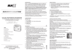
The AFE5801EVM is an evaluation tool designed for the ultrasound analog front-end (AFE) device
AFE5801. In order to deserialize the outputs of AFE5801, an ADSDeSer-50EVM or TSW1250EVM is
needed during the evaluation.
Contents
Introduction .................................................................................................................. 3
1.1
AFE5801EVM Kit Contents ....................................................................................... 3
1.2
Features ............................................................................................................. 3
1.3
Power Supplies ..................................................................................................... 3
1.4
Indicators ............................................................................................................ 3
2
Board Configuration ........................................................................................................ 5
2.1
Board Connections Overview .................................................................................... 5
2.2
I/O and Power Connectors ....................................................................................... 6
2.3
Jumpers and Setup ................................................................................................ 7
2.4
Test Points .......................................................................................................... 9
3
Board Operation ............................................................................................................. 9
3.1
Software Installation and Operation ............................................................................. 9
3.2
USB Driver Installation ............................................................................................ 9
3.3
GUI Startup ........................................................................................................ 11
3.4
Hardware Setup .................................................................................................. 14
3.5
Clock Selection ................................................................................................... 14
3.6
Data Analysis ..................................................................................................... 15
4
Schematics, Layout, and, Bill of Materials ............................................................................. 16
4.1
Schematics ........................................................................................................ 16
4.2
PCB Layout ........................................................................................................ 22
4.3
Bill of Materials .................................................................................................... 30
5
Typical Performance ...................................................................................................... 32
Appendix A
TSW1250 for Evaluating AFE5801 ............................................................................. 33
Appendix B
TSW1100 for Evaluating AFE5801 ............................................................................. 42
1
List of Figures
1
AFE5801EVM LED Locations ............................................................................................. 4
2
AFE5801EVM TOP View
3
4
5
6
7
8
9
10
11
..................................................................................................
AFE5801EVM BOTTOM View ............................................................................................
Locations of Jumpers, Headers and Switches on the AFE5801EVM ................................................
Default Setup for Jumpers .................................................................................................
Found New Hardware Wizard Screen....................................................................................
Found New Hardware Wizard (Next) Screen ..........................................................................
...............................................................................................................................
AFE5801EVM USB SPI Interface for General Registers. ............................................................
AFE5801EVM USB SPI Fixed Gain Mode .............................................................................
AFE5801EVM USB SPI Interface for Variable Gain Mode ..........................................................
5
5
8
8
9
10
10
12
13
13
Windows XP is a trademark of Microsoft Corporation.
SLOU257 – October 2009
Submit Documentation Feedback
AFE5801 8-Channel Variable Gain Amplifier (VGA) with Octal High-Speed ADC
Copyright © 2009, Texas Instruments Incorporated
1
www.ti.com
........................................................................................
12
Typical AFE5801 Bench Setup:
13
Clock Selection Jumper Configurations: (a) Transformer (default); (b) Single-ended Clock; (c) Future
CLK Input Option Based on U1. Both (b) and (c) Configurations Need Some Modifications on the PCB. .... 14
14
Schematic Page 1 ......................................................................................................... 17
15
Schematic Page 2 ......................................................................................................... 18
16
Schematic Page 3 ......................................................................................................... 19
17
Schematic Page 4 ......................................................................................................... 20
18
Schematic Page 5 ......................................................................................................... 21
19
Schematic Page 6 ......................................................................................................... 21
20
Top Layer Signal
21
Inner Layer 1 Ground ..................................................................................................... 24
22
Inner Layer 2 Signal ....................................................................................................... 25
23
Inner Layer 3 Power
24
25
26
27
28
29
30
31
32
33
34
35
36
37
38
39
40
41
42
43
..........................................................................................................
......................................................................................................
Inner Layer 4 Ground .....................................................................................................
Bottom Layer Signal.......................................................................................................
Top Silk Screen Layer ....................................................................................................
Bottom Silk Screen Layer ................................................................................................
Typical Performance of AFE5801. (a) Fixed Gain Mode; (b) Variable Gain Mode ...............................
Connection Between TSW1250EVM and AFE5801 ..................................................................
Connection of the Instruments ...........................................................................................
AFE5801EVM GUI - RUN Mode ........................................................................................
AFE5801 EVM GUI - START Button ...................................................................................
AFE5801EVM GUI - Variable Gain .....................................................................................
AFE5801EVM GUI - Setting Fixed Gain ...............................................................................
User Interface: Initial Setup Screen .....................................................................................
User Interface: Step-by-Step Setup .....................................................................................
User Interface: Frequency Load Value to Signal Generator .........................................................
User Interface: Final Setup Screen .....................................................................................
User Interface: Single FFT Format ......................................................................................
User Interface: Time Domain Format ...................................................................................
Plot of Saved Sample Data ..............................................................................................
TSW1100 Interface ........................................................................................................
Analysis of Non-Coherent Sampled Data. (a) No window applied; (b) Hanning window applied. .............
14
23
26
27
28
29
29
32
33
34
34
35
36
37
38
38
39
40
40
41
41
44
45
List of Tables
1
2
Channel-to-Channel Matching Between the AFE5801EVM and ADSDeSER-50EVM ........................... 14
AFE5801 8-Channel Variable Gain Amplifier (VGA) with Octal High-Speed ADC
Copyright © 2009, Texas Instruments Incorporated
SLOU257 – October 2009
Submit Documentation Feedback
Introduction
www.ti.com
1
Introduction
AFE5801 includes an 8-channel voltage-Controlled-Amplifier (VCA) with digital control and an 8-channel
65MSPS analog-to-digital converter (ADC). The outputs of the ADC are 8-channel LVDS outputs which
should be deserialized by the ADSDeSer-50EVM or TSW1250EVM. The AFE5801EVM provides an easy
way to examine the performances and functionalities of AFE5801.
1.1
AFE5801EVM Kit Contents
The AFE5801EVM kit contains the following:
• AFE5801 EVM board
• USB cable
• CD-ROM containing
– AFE5801 EVM User’s Guide (this document)
– GUI software
1.2
Features
•
•
•
•
•
1.3
Characterize AFE5801
Provide 8-channel LVDS outputs from the ADC
Compatible to the standard TI LVDS deserializer ADSDeSer-50EVM or TSW1250EVM
Communicate with PC through USB interface
Power Management provides multiple power supplies for AFE5801 and other devices.
Power Supplies
The AFE5801EVM requires only +5V power supplies for operation.
1.4
Indicators
The AFE5801EVM has 4 LEDs on the board as shown in Figure 1. Their states demonstrate the normal
operation of AFE5801EVM.
• LED 1: U1 status indicator. Its ON state indicates the clock management chip U1 works well if U1 is
installed.
• LED 3 and 2 (RED): 1.8VD and 1.8VA power supply indicators. ON state indicates that the AFE5801
is powered correctly.
• LED 4 (GREEN): +3.3V power supply indicator. ON state indicates that the AFE5801 is powered
correctly.
SLOU257 – October 2009
Submit Documentation Feedback
AFE5801 8-Channel Variable Gain Amplifier (VGA) with Octal High-Speed ADC
Copyright © 2009, Texas Instruments Incorporated
3
Introduction
www.ti.com
LED3 LED4
LED 2
LED 1
Figure 1. AFE5801EVM LED Locations
4
AFE5801 8-Channel Variable Gain Amplifier (VGA) with Octal High-Speed ADC
Copyright © 2009, Texas Instruments Incorporated
SLOU257 – October 2009
Submit Documentation Feedback
Board Configuration
www.ti.com
2
Board Configuration
This chapter describes the locations and functionalities of inputs, outputs, jumpers, test points of the
AFE5801EVM in detail.
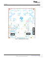
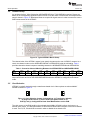
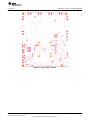
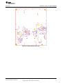
2.1
Board Connections Overview
Input
Signals
+5V
PWR
Low Jitter
Clk In
DUT
USB
Ext Clk In
Figure 2. AFE5801EVM TOP View
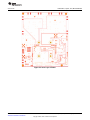
AFE/TSW
Adapter
Connector
Figure 3. AFE5801EVM BOTTOM View
SLOU257 – October 2009
Submit Documentation Feedback
AFE5801 8-Channel Variable Gain Amplifier (VGA) with Octal High-Speed ADC
Copyright © 2009, Texas Instruments Incorporated
5
Board Configuration
2.2
www.ti.com
I/O and Power Connectors
The positions and functions of the AFE5801EVM connectors are discussed in this section.
• Analog Inputs Ch1~Ch8 (J1~J8): Single-end analog signal is converted to differential signals by
transformer.
• Low Jitter CLK Source Input (J11): This input accepts clocks with low jitter noise, such as HP8644
output. 20~50MHz 50% duty cycle clock with 1~2Vrms amplitude can be used. When J11 is used,
make sure shunts P4, P5, P6 are removed.
• CLK output (J10): The output of either the U1 output or the on-board 40MHz oscillator output
depending on jumper P4’s connection.
• External CLK Input (J9): ADC Clock input, such as FPGA outputs. FPGA outputs must be processed
by U1. Otherwise, the ADC of AFE5801 will not achieve satisfactory performance.
• +5V PWR connector(P10): Power supply input
• USB input (P11): USB interface to control the AFE5801.
• LVDS Outputs Ch1~Ch8 (P13): Differential LVDS data outputs.
6
AFE5801 8-Channel Variable Gain Amplifier (VGA) with Octal High-Speed ADC
Copyright © 2009, Texas Instruments Incorporated
SLOU257 – October 2009
Submit Documentation Feedback
Board Configuration
www.ti.com
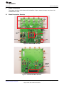
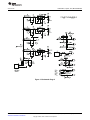
2.3
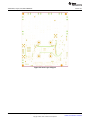
Jumpers and Setup
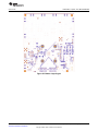
The board has been set to default mode. Detailed description can be found in Figure 4 and Figure 5.
P15
P14
P8
P2
P3
P12
P4
SW1
P1
P9
P7
P5
P6
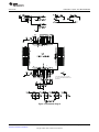
Figure 4. Locations of Jumpers, Headers and Switches on the AFE5801EVM
SLOU257 – October 2009
Submit Documentation Feedback
AFE5801 8-Channel Variable Gain Amplifier (VGA) with Octal High-Speed ADC
Copyright © 2009, Texas Instruments Incorporated
7
Board Configuration
www.ti.com
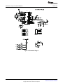
Figure 5. Default Setup for Jumpers
•
•
•
•
•
•
•
•
•
8
P1: SPI interface for U1
P2, P3: AFE5801 ADC clock input selection: transformer-based differential clock, single-ended
LVCMOS clock, or future clock option (needs U1 to support). Default is to use transformer-based
differential clock.
P4: Select jitter-cleaned clock or non-jitter-cleaned clock. Default is to use non-jitter-cleaned clock (i.e.,
on-board 40MHz clock).
P5: Use on-board 40MHz clock. Default is that the on-board clock is used.
P6: Power on on-board 40MHz clock generator. Default is on.
P8: Debug port for monitoring ADS SPI signals.
P9: USB interface enable. Default is on.
Regulated power supply outputs (P12, P7): 1.8VA, 1.8VD, and 3.3V. P12 and P7 can be configured as
power supply input as well if users would like to skip the on-board regulators. Remove the ferrite beads
L1, L2, L3, L7 and L24,
SW1: Reset switch for AFE5801.
AFE5801 8-Channel Variable Gain Amplifier (VGA) with Octal High-Speed ADC
Copyright © 2009, Texas Instruments Incorporated
SLOU257 – October 2009
Submit Documentation Feedback
Board Operation
www.ti.com
2.4
Test Points
•
3
Multiple Test Points are provided on the EVM. Refer to the attached schematics for more information.
Board Operation
This chapter describes how to operate the AFE5801EVM for evaluation. Both software and hardware
installation and operation are discussed.
3.1
Software Installation and Operation
The AFE5801EVM comes with a software install CD; run setup.exe to install the software.
3.2
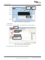
USB Driver Installation
•
•
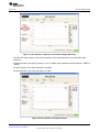
•
Connect the USB port of EVM to your PC.
If the driver has not been installed then the message “Windows Found New Hardware” will appear.
The Wizard as the following picture will launch.
Select "No, not this time" from the options. Press Next button
Figure 6. Found New Hardware Wizard Screen
•
Select "Install from a list or specific location (Advanced)" as shown below and then click "Next".
SLOU257 – October 2009
Submit Documentation Feedback
AFE5801 8-Channel Variable Gain Amplifier (VGA) with Octal High-Speed ADC
Copyright © 2009, Texas Instruments Incorporated
9
Board Operation
www.ti.com
Figure 7. Found New Hardware Wizard (Next) Screen
•
•
Select "Search for the best driver in these locations" and enter the file path for ("C:\Program
Files\AFE5801\CDM 2.04.06 WHQL Certified ") in the combo-box or browse to it by clicking the browse
button. Once the file path has been entered in the box, click next to proceed.
If Windows XP™ is configured to warn when unsigned (non-WHQL certified) drivers are about to be
installed, the following screen will be displayed unless installing a Microsoft WHQL certified Driver.
Click on "Continue Anyway" to continue with the installation. If Windows XP is configured to ignore file
signature warnings, no message will appear.
Figure 8.
10
AFE5801 8-Channel Variable Gain Amplifier (VGA) with Octal High-Speed ADC
Copyright © 2009, Texas Instruments Incorporated
SLOU257 – October 2009
Submit Documentation Feedback
Board Operation
www.ti.com
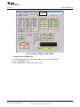
3.3
GUI Startup
•
•
•
Launch GUI from XP Window
Start → All Programs\AFE5801EVM\AFE5801
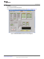
Several different screens appear displaying the different modes (Figure 9 through Figure 11)
Figure 9. AFE5801EVM USB SPI Interface for General Registers.
SLOU257 – October 2009
Submit Documentation Feedback
AFE5801 8-Channel Variable Gain Amplifier (VGA) with Octal High-Speed ADC
Copyright © 2009, Texas Instruments Incorporated
11
Board Operation
www.ti.com
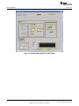
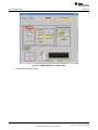
Figure 10. AFE5801EVM USB SPI Fixed Gain Mode
12
AFE5801 8-Channel Variable Gain Amplifier (VGA) with Octal High-Speed ADC
Copyright © 2009, Texas Instruments Incorporated
SLOU257 – October 2009
Submit Documentation Feedback
Board Operation
www.ti.com
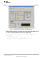
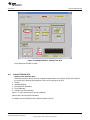
Figure 11. AFE5801EVM USB SPI Interface for Variable Gain Mode
When AFE5801EVM is powered on, all registers have been set to their default modes. Refer to the
datasheet for all default settings. It is recommended to restart the SPI software when AFE5801 is powered
on in order to synchronize the AFE5801 register settings to the software displays.
Users also can fill out Address Bytes and Data Bytes and press ENTER to configure each register.
Typical Configuration
• From Figure 9 press "Init for TSW1250" button
• Select TAB “TGC Register” - Figure 10 will appear
• From Figure 11, press “Variable” button to get into fixed gain mode
• From Figure 10 enter 30 in the “Coarse Gain(dB)” field then press “Write” button.
SLOU257 – October 2009
Submit Documentation Feedback
AFE5801 8-Channel Variable Gain Amplifier (VGA) with Octal High-Speed ADC
Copyright © 2009, Texas Instruments Incorporated
13
Board Operation
3.4
www.ti.com
Hardware Setup
As mentioned before, Xilinx DeSerializer ADSDeSER-50EVM or TSW1250EVM is required. Please see
details in the corresponding application notes on how to use the either of these EVMs. An example bench
setup is shown in Figure 12. Band-pass filters are required for signal source in order to ensure the correct
SNR measurements of the AFE5801.
Figure 12. Typical AFE5801 Bench Setup:
The channel order of the AFE5801 outputs is not exactly the same as the one of ADS527x outputs. As a
result, the channel number on the ADSDeSER-50EVM or AFE5801EVM might be misleading. Table 1
provides channel-to-channel sequence matching between the ADSDeSER-50EVM and AFE5801EVM.
Table 1. Channel-to-Channel Matching Between the AFE5801EVM and ADSDeSER-50EVM
AFE
FCLK
CH1
CH2
CH3
CH4
CH5
CH6
CH7
CH8
LCLK
Xilinx
FCLK
CH8
CH7
CH6
CH5
CH4
CH3
CH2
CH1
LCLK
For example, when an analog signal is input at CH1 on the AFE5801EVM, the corresponding 12-bit digital
output will be seen at CH8 on the ADSDeSER-50EVM when the AFE5801 is configured as 8-channel
mode.
3.5
Clock Selection
AFE5801 is typically clocked through a transformer-based circuit. Other options are also available if
needed as shown in Figure 13.
(a)
(b)
(c)
Figure 13. Clock Selection Jumper Configurations: (a) Transformer (default);
(b) Single-ended Clock; (c) Future CLK Input Option Based on U1.
Both (b) and (c) Configurations Need Some Modifications on the PCB.
The clock source of the EVM could be the on-board clock 40MHz, HP8644 low jitter clock source, or
external clock source. The best performance of this EVM is achieved when low-jitter clock source HP8644
is used. The P4, P5, P6 should be removed in order to disable the on-board clock.
14
AFE5801 8-Channel Variable Gain Amplifier (VGA) with Octal High-Speed ADC
Copyright © 2009, Texas Instruments Incorporated
SLOU257 – October 2009
Submit Documentation Feedback
Board Operation
www.ti.com
When HP8644 or similar clock sources are not available, the on-board 40MHz clock is also a desirable
source. The jumpers P4, 5, 6 should be configured as Figure 13 shows (i.e., default setup for
AFE5801EVM). In this mode, the transform-based differential clock is used.
3.6
Data Analysis
Based on the data file acquired by a logic analyzer, the performance of AFE5801 can be evaluated.
In Appendix A, we provide one solution (TI TSW1250 EVM) to analyze the data file using the PC.
Appendix B provides an alternate solution (TI TSW1100 software) to analyze the data file captured by a
logic analyzer. Coherent sampling is recommended if the input and sampling clock are phase locked. Due
to the frequency accuracy requirement of coherence sampling, two HP8644s for generating ADC clock
and analog signal are required. For most users, this may not be feasible. Data analysis based on
windowing is a more suitable approach.
SLOU257 – October 2009
Submit Documentation Feedback
AFE5801 8-Channel Variable Gain Amplifier (VGA) with Octal High-Speed ADC
Copyright © 2009, Texas Instruments Incorporated
15
Schematics, Layout, and, Bill of Materials
4
www.ti.com
Schematics, Layout, and, Bill of Materials
This chapter provides the schematics and layout of the AFE5801EVM as well as the bill of materials.
4.1
Schematics
Figure 14. Schematic Page 1
16
AFE5801 8-Channel Variable Gain Amplifier (VGA) with Octal High-Speed ADC
Copyright © 2009, Texas Instruments Incorporated
SLOU257 – October 2009
Submit Documentation Feedback
Schematics, Layout, and, Bill of Materials
www.ti.com
Figure 15. Schematic Page 2
SLOU257 – October 2009
Submit Documentation Feedback
AFE5801 8-Channel Variable Gain Amplifier (VGA) with Octal High-Speed ADC
Copyright © 2009, Texas Instruments Incorporated
17
Schematics, Layout, and, Bill of Materials
www.ti.com
Figure 16. Schematic Page 3
18
AFE5801 8-Channel Variable Gain Amplifier (VGA) with Octal High-Speed ADC
Copyright © 2009, Texas Instruments Incorporated
SLOU257 – October 2009
Submit Documentation Feedback
Schematics, Layout, and, Bill of Materials
www.ti.com
Figure 17. Schematic Page 4
SLOU257 – October 2009
Submit Documentation Feedback
AFE5801 8-Channel Variable Gain Amplifier (VGA) with Octal High-Speed ADC
Copyright © 2009, Texas Instruments Incorporated
19
Schematics, Layout, and, Bill of Materials
www.ti.com
Figure 18. Schematic Page 5
20
AFE5801 8-Channel Variable Gain Amplifier (VGA) with Octal High-Speed ADC
Copyright © 2009, Texas Instruments Incorporated
SLOU257 – October 2009
Submit Documentation Feedback
Schematics, Layout, and, Bill of Materials
(1)
www.ti.com
(1) Pin 28 may also be connected
to 1.8 V per the AFE5801 data sheet,
(SLOS591).
Figure 19. Schematic Page 6
SLOU257 – October 2009
Submit Documentation Feedback
AFE5801 8-Channel Variable Gain Amplifier (VGA) with Octal High-Speed ADC
Copyright © 2009, Texas Instruments Incorporated
21
Schematics, Layout, and, Bill of Materials
4.2
www.ti.com
PCB Layout
A
•
•
•
•
•
•
•
•
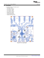
six-layer printed-circuit board is used:
Top Layer, signal
Inner Layer 1, ground
Inner Layer 2, signal
Inner Layer 3, power
Inner Layer 4, ground
Bottom Layer, signal
Top Silk Screen Layer
Bottom Silk Screen Layer
Figure 20. Top Layer Signal
22
AFE5801 8-Channel Variable Gain Amplifier (VGA) with Octal High-Speed ADC
Copyright © 2009, Texas Instruments Incorporated
SLOU257 – October 2009
Submit Documentation Feedback
Schematics, Layout, and, Bill of Materials
www.ti.com
Figure 21. Inner Layer 1 Ground
SLOU257 – October 2009
Submit Documentation Feedback
AFE5801 8-Channel Variable Gain Amplifier (VGA) with Octal High-Speed ADC
Copyright © 2009, Texas Instruments Incorporated
23
Schematics, Layout, and, Bill of Materials
www.ti.com
Figure 22. Inner Layer 2 Signal
24
AFE5801 8-Channel Variable Gain Amplifier (VGA) with Octal High-Speed ADC
Copyright © 2009, Texas Instruments Incorporated
SLOU257 – October 2009
Submit Documentation Feedback
Schematics, Layout, and, Bill of Materials
www.ti.com
Figure 23. Inner Layer 3 Power
SLOU257 – October 2009
Submit Documentation Feedback
AFE5801 8-Channel Variable Gain Amplifier (VGA) with Octal High-Speed ADC
Copyright © 2009, Texas Instruments Incorporated
25
Schematics, Layout, and, Bill of Materials
www.ti.com
Figure 24. Inner Layer 4 Ground
26
AFE5801 8-Channel Variable Gain Amplifier (VGA) with Octal High-Speed ADC
Copyright © 2009, Texas Instruments Incorporated
SLOU257 – October 2009
Submit Documentation Feedback
Schematics, Layout, and, Bill of Materials
www.ti.com
Figure 25. Bottom Layer Signal
SLOU257 – October 2009
Submit Documentation Feedback
AFE5801 8-Channel Variable Gain Amplifier (VGA) with Octal High-Speed ADC
Copyright © 2009, Texas Instruments Incorporated
27
Schematics, Layout, and, Bill of Materials
www.ti.com
Figure 26. Top Silk Screen Layer
28
AFE5801 8-Channel Variable Gain Amplifier (VGA) with Octal High-Speed ADC
Copyright © 2009, Texas Instruments Incorporated
SLOU257 – October 2009
Submit Documentation Feedback
Schematics, Layout, and, Bill of Materials
www.ti.com
Figure 27. Bottom Silk Screen Layer
SLOU257 – October 2009
Submit Documentation Feedback
AFE5801 8-Channel Variable Gain Amplifier (VGA) with Octal High-Speed ADC
Copyright © 2009, Texas Instruments Incorporated
29
Schematics, Layout, and, Bill of Materials
4.3
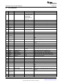
Bill of Materials
ITEM
MFG
1
30
www.ti.com
MFG PART#
REF DES
VALUE or FUNCTION
UNINSTALLED
C98–C105
Capacitor, SMT, 0402 Uninstalled
2
Kemet
C0402C104K8PAC
C1–C5, C8, C9, C12,
C13, C16, C17, C19,
C20, C24–C28,
C31–C44, C46,
C48–C53, C56–C95,
C107–C114
Capacitor, SMT, 0402, Ceramic, 0.1μF, 10V, 10%, X5R
3
Murata
GRM155R60J225ME15D
C23
Capacitor, SMT, 0402, Ceramic, 2.2 μF, 6.3V, 20%, X5R
4
Panasonic
ECJ-1VB0J475K
C29
Capacitor, SMT, 0603, Ceramic, 4.7 μF, 6.3V, 10%, X5R
5
Panasonic
ECJ-1VB1A105K
C54, C55, C96, C106
Capacitor, SMT, 0603, Ceramic, 1.0 μF, 10V, 10%, X5R
6
Taiyo Yuden
JMK107BJ106MA-T
C21, C22
Capacitor, SMT, 0603, Ceramic, 10 μF, 6.3V, 20%, X5R
7
Murata
GRM31CR60J476ME19B
C30
Capacitor, SMT, Ceramic, 1206, 47 μF, 6.3V, 20%, X5R
8
Vishay
Sprage
293D106X5035D2T
C97, C115
Capacitor, TAN, SMT, 10uF, 35V, ±5%, –55~85C
9
AVX
TPSC226K016R0375
C6, C7, C10, C11, C14,
C15, C18, C45, C47
10%, 16V, 22μF
10
Samtec
SMA-J-P-X-ST-EM1
J1–J9
SMA Jack, Edge mount, 062PCB, Brass/Gold, Straight, 50 Ω
11
Samtec
SMA-J-P-H-ST-TH1
J10–J12
SMA Coax straight PCB Jack, SMT, 175TL, 50 Ω, Gold
12
Advanced
Connectek
MNE20-5K5P10
P11
MINI-AB USB OTG Receptacle R/A SMT Type
13
Samtec
QTH-040-01-L-D-DP-A
P13
Connector, SMT, 80P, 0,5mm, FEM, DIFF Pair, Receptacle,
168H
14
Epson
Toyocom
HF-372A
F1
(Customer Supply) Crystal filter miniature radio Equipment/IF
15
TI
DUT_QFP-48_0.5mmLS
U1
DUT, SMT, 48P, 0,5mm LS, 7.15×7.15×1mm (Customer
Supply)
16
Not Installed
PAD0201(UN)
EP2, EP3
( Uninstalled Part ) Empty pad, SMT, 0201
17
Murata
BLM15BD102SN1D
L9–L20
Ferrite bead, SMT, 0402, 1kΩ, 200 mA
18
Murata
BLM18EG601SN1D
L8
Ferrite bead, SMT, 0603,600 Ω at 100 MHz, 25%, 800 mA
19
Steward
HI0805R800R-00
L1–L7, L21, L22,
L24–L26
Ferrite, SMT, 0805, 80 Ω at 100 MHz, 5 A
20
Steward
LI1206H151R-00
L23
Ferrite, SMT, 1206, 150 Ω at 100 MHz, 0.8 A
21
Molex
39357-0002
P10
Header, THRU, Power, 2P, 3.5MM, Eurostyle
22
Samtec
SSQ-104-02-F-D
P1
Header, THU, 8P, 2X4, 100LS, FEM, VERT, 194TL
23
Samtec
TSW-103-08-G-D
P2, P3
Header, THU, 6P, 2X3, male, dual row, 100LS, 200TL
24
Tyco
Electronics
103321-2
P6, P9
Header w/shunt, 2P, 100LS
25
Molex
22-23-2021-P
P7
MALE, 2PIN, 0.100CC w/ friction lock
26
Mill-Max
350-10-103-00-006
P4, P5
Header, THU, MAL, 0.1LS, 3P, 1X3, 284H, 110TL
27
Molex
22-23-2041
P12
4P, VERT, Friction lock
28
Samtec
TSW-108-05-G-S
P8
Header, THU, 8P, 1X8, male, single row, 100LS, 130TL
29
TI
TPS79618DCQR
U5
Ultralow-noise HI PSRR Fast RF 1-A LDO Linear regulator,
1.8V
30
TI
TPS79633DCQR
U4
Ultralow-noise HI PSRR Fast RF 1-A LDO Linear regulator,
3.3V
31
TI
TPS79318DBV
U3 (UNINSTALLED)
1.8V,Ultralow-noise HI PSRR Fast RF 200 mA LDO Linear
regulator
32
Future
Technology
Device Int.
FT245RL
U6
USB FIFO IC Incorporate FTDICHIP-ID Security dongle
33
Any
JUMPER,2P 0.100cc
EP5, EP6
Installed any brand 2PIN THU Jumper
34
Any
JUMPER,3P 0.100cc 123
P14, P15
Installed jumper, THU, 3P 0.100cc, 123
AFE5801 8-Channel Variable Gain Amplifier (VGA) with Octal High-Speed ADC
Copyright © 2009, Texas Instruments Incorporated
SLOU257 – October 2009
Submit Documentation Feedback
Schematics, Layout, and, Bill of Materials
www.ti.com
ITEM
MFG
MFG PART#
REF DES
VALUE or FUNCTION
35
Panasonic
LNJ308G8PRA
LED1, LED4
LED, SMT, 0603, pure green, 2.03V
36
Panasonic
LNJ808R8ERA
LED2, LED3
LED, SMT, 0603, orange, 1.8V
37
ECS
ECS-3953M-400-BN
U2
OSC, SMT, 3.3V, 50ppm, -40~85C, 5nS, 40.000 MHz
38
Vishay
CRCW04021002F100
R28, R29, R30
Resistor, SMT, 0402, 10K, 1/16W, 1%, 100ppm
39
Panasonic
ERJ-2GE0R00X
R8, R10–R12, R15,
R19, R20, R32, R44,
R45, R48, R49, R52,
R53, R56, R57, R60,
R61, R64, R65, R68,
R69, R72, R73, R76,
R77, R79, R80
Resistor/jumper,SMT, 0402, 0 Ω, 5%, 1/16W
40
Panasonic
ERJ-2GEJ0000(UN)
R5, R7, R9, R14, R17,
R18
( UNINSTALLED PART )
41
Panasonic
ERJ-2GEJ131
R21, R22
Resistor, SMT, 0402, thick film, 5%, 1/16W, 130
42
Panasonic
ERJ-2GEJ49R9(UN)
R25, R36–R43
( UNINSTALLED PART )
43
Panasonic
ERJ-2GEJ820
R23, R24
Resistor, SMT, 0402, thick film, 5%, 1/16W, 82
44
Panasonic
ERJ-2RKF1000X
R2, R3
Resistor, SMT, 0402, 100 Ω, 1%, 1/16W
45
Panasonic
ERJ-2RKF1001X
R4
Resistor, SMT, 0402, 1.00K, 1%, 1/16W
46
Panasonic
ERJ-2RKF25R5X
R46,
R54,
R62,
R70,
47
Panasonic
ERJ-2RKF3320X
R1, R6, R16
Resistor, SMT, 0402 332 Ω, 1%, 1/16W
48
Panasonic
ERJ-2RKF49R9X
R26, R27, R33
Resistor, SMT, 0402, 49.9 Ω, 1%, 1/16W
49
Panasonic
ERJ-3GSYJ100
R78
Resistor, SMT, 0603, 5%, 1/10W, 10
50
Vishay
CRCW08051002F
R31, R34, R35
Resistor, SMT, 0805, thick film, 1%, 1/8W, 10.0K
51
Panasonic
ERJ-6RQF5R1V
R13
Resistor, SMT, 0805, 1%, 1/8W, 5.1 Ω
52
Panasonic
ERJ-1GE0R00C
EP1, EP4
Resistor, SMT, 0201, thick film, 0 Ω, 5%,0 Ω Jumper, 1/20W
53
Handtest
Only
Socket, 9X9, 64RTD,
Handtest
AFE5801
AFE5801
54
ITT
Industries
PTS635SK25SM
SW1
Switch, SMT, 2P, SPST-NO, 2.5mm Height, MOM,
rectangular, 0.05A, 12V
55
Keystone
Electronics
5005
TP1
Testpoint, THU, compact, 0.125LS, 130TL, red
56
Keystone
Electronics
5006
TP2–TP6
Testpoint, THU, compact, 0.125LS, 130TL, black
57
Mini-Circuits
ADTT1-1
T1–T8
RF Transformer 0.03–300 MHz
58
Mini-Circuits
ADT1-6T
T9
RF Transformer wideband, 0.03–125 MHz
SLOU257 – October 2009
Submit Documentation Feedback
R47,
R55,
R63,
R71,
R50,
R58,
R66,
R74,
R51,
R59,
R67,
R75
Resistor, SMT, 0402, 25.5 Ω, 1%, 1/16W
AFE5801 8-Channel Variable Gain Amplifier (VGA) with Octal High-Speed ADC
Copyright © 2009, Texas Instruments Incorporated
31
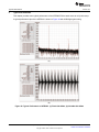
Typical Performance
5
www.ti.com
Typical Performance
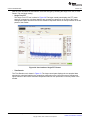
This chapter provides some typical performance of the AFE5801EVM to assist users to verify their setup.
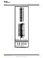
A typical performance plot of the AFE5801 is shown in Figure 28 with 30dB digital gain setting.
(a)
(b)
Figure 28. Typical Performance of AFE5801. (a) Fixed Gain Mode; (b) Variable Gain Mode
32
AFE5801 8-Channel Variable Gain Amplifier (VGA) with Octal High-Speed ADC
Copyright © 2009, Texas Instruments Incorporated
SLOU257 – October 2009
Submit Documentation Feedback
Appendix A
www.ti.com
Appendix A TSW1250 for Evaluating AFE5801
A.1
Introduction
This application report goes through the steps of evaluating the AFE501 using the TSW1250EVM.
A.2
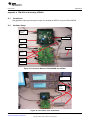
Hardware Setup
USB
Interf ace of
TSW1250
+6V supply
TSW1250
Bridge
board
Filter
USB
Interface
+5V from
TSW1250
AFE5801
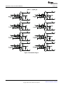
Figure 29. Connection Between TSW1250EVM and AFE5801
Clock source
40MHz
Analog
Signal
to Filter
Figure 30. Connection of the Instruments
SLOU257 – October 2009
Submit Documentation Feedback
TSW1250 for Evaluating AFE5801
Copyright © 2009, Texas Instruments Incorporated
33
Launch AFE5801 GUI
A.3
www.ti.com
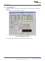
Launch AFE5801 GUI
From PC click Start Menu→All Programs→Texas Instruments→AFE5801EVM USB SPI→AFE5801EVM
USB SPI
The GUI may be running if the following screen appears:
Figure 31. AFE5801EVM GUI - RUN Mode
In case the GUI is not running, then press the START button of the GUI to run it.
34
TSW1250 for Evaluating AFE5801
SLOU257 – October 2009
Submit Documentation Feedback
Copyright © 2009, Texas Instruments Incorporated
Launch AFE5801 GUI
www.ti.com
START
BUTTON
Figure 32. AFE5801 EVM GUI - START Button
•
1.
2.
3.
Commands to the AFE5801 GUI:
Click Init for TSW1250 to set the proper condition to work with TSW1250EVM.
Go to "TGC Register " Tab.
Press Variable button to change the mode to Fixed.
SLOU257 – October 2009
Submit Documentation Feedback
TSW1250 for Evaluating AFE5801
Copyright © 2009, Texas Instruments Incorporated
35
Launch AFE5801 GUI
www.ti.com
Figure 33. AFE5801EVM GUI - Variable Gain
4. Type 30 and press Write button.
36
TSW1250 for Evaluating AFE5801
SLOU257 – October 2009
Submit Documentation Feedback
Copyright © 2009, Texas Instruments Incorporated
Launch TSW1250 GUI
www.ti.com
Figure 34. AFE5801EVM GUI - Setting Fixed Gain
At this stage the AFE5801 is ready.
A.4
Launch TSW1250 GUI
•
1.
2.
3.
4.
5.
Graphics User Interface (GUI)
TSW1250 provides a GUI for users to evaluate the performance of the device. When GUI is started,
the screen of the following figure appears. There are five groups of the GUI:
Toolbar
Message Window
Device Specific Selections
Test Parameters
Central Pane and result data
Items 1, 3, and 4 are used to set up test conditions.
Items 2 and 5 are test results and status.
For details, see the TSW1250 User's Guide included in the CD.
SLOU257 – October 2009
Submit Documentation Feedback
TSW1250 for Evaluating AFE5801
Copyright © 2009, Texas Instruments Incorporated
37
Launch TSW1250 GUI
www.ti.com
Time
Domain Test
Tab
Frequency
Domain Test
Tab
Display of
test result
Figure 35. User Interface: Initial Setup Screen
•
Test Condition
Perform the steps in the order indicated in the following figure to set the test conditions:
1. Select
AFE5801
2. Enter 40M
3. Enter 2M
4. Select 16384
5. Uncheck and then
Check To calculate
coherent Frequency
Figure 36. User Interface: Step-by-Step Setup
After completing the five steps indicated, the following figure appears:
38
TSW1250 for Evaluating AFE5801
SLOU257 – October 2009
Submit Documentation Feedback
Copyright © 2009, Texas Instruments Incorporated
Launch TSW1250 GUI
www.ti.com
Figure 37. User Interface: Frequency Load Value to Signal Generator
Take the ADC Input frequency, and set the frequency of the signal generator to the noted ADC Input
frequency.
Set the Amplitude of the signal generator to -18 to -20 dBm (input amplitude should be between -1dBFS to
-3dbFS)
Set the Frequency of the Clock Generator to 40 MHz.
Set the Amplitude of the Clock Generator to 13 dBm.
Figure 38. User Interface: Final Setup Screen
SLOU257 – October 2009
Submit Documentation Feedback
TSW1250 for Evaluating AFE5801
Copyright © 2009, Texas Instruments Incorporated
39
Launch TSW1250 GUI
www.ti.com
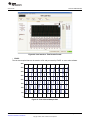
Now the user can select the test channel, select the test type by choosing the Single Tone Tab, or Time
Domain Tab, and begin testing.
• Single Tone FFT
The Single Tone FFT test is shown in Figure 39. The larger central pane displays the FFT power
spectrum, whereas the calculated statistics are grouped into categories on the right of the screen.
Settings and inputs relevant to the test are entered in drop-down menus or text input boxes on the left
portion of the window.
Figure 39. User Interface: Single FFT Format
•
Time Domain
The Time Domain test is shown in Figure 40. The larger central pane displays the raw sampled data
whereas the calculated statistics are grouped into categories on the right of the screen. Settings and
inputs relevant to the test are entered in drop-down menus or text input boxes on the left portion of the
window.
40
TSW1250 for Evaluating AFE5801
SLOU257 – October 2009
Submit Documentation Feedback
Copyright © 2009, Texas Instruments Incorporated
Launch TSW1250 GUI
www.ti.com
Figure 40. User Interface: Time Domain Format
•
EXCEL
The raw test sampled data can be saved to a file and processed by EXCEL or some other software.
4000
3500
3000
2500
2000
1500
1000
500
0
0
10
20
30
40
50
60
70
80
90
100
Figure 41. Plot of Saved Sample Data
SLOU257 – October 2009
Submit Documentation Feedback
TSW1250 for Evaluating AFE5801
Copyright © 2009, Texas Instruments Incorporated
41
Appendix B
www.ti.com
Appendix B TSW1100 for Evaluating AFE5801
B.1
Introduction
This appendix describes the use of TSW1100 software to analyze data files acquired by logic analyzers.
As mentioned before, coherent sampling is recommended when HP8644s are used. The calculation of
coherent sampling rate and signal frequency can be found in the TSW1100 user manual at following
website:
http://focus.ti.com/docs/toolsw/folders/print/tsw1100.html
Users can set the calculated frequencies for signal generators; acquire ADC data through a logic analyzer;
and save the data as a txt file. Typical data file captured by logic analyzer should be modified to the
following format (i.e., containing only one column):
1981
1615
1292
1046
895
852
927
1113
1394
1737
2110
2477
2798
3044
3196
3237
3162
2978
.
.
.
.
42
TSW1100 for Evaluating AFE5801
SLOU257 – October 2009
Submit Documentation Feedback
Copyright © 2009, Texas Instruments Incorporated
Introduction
www.ti.com
The AFE5801 performance analysis can be done as follows:
• First of all, some header information should be added to the modified logic analyzer data file as per the
following. Example files were included in the TSW1100 software package. Time, sampling rate,
frequency, and 2’s complement should be modified based on your setup. An example data file is listed
below.
TSW1000
2/12/2007 12:38
Bits =12
Sampling Rate =40000000.000
Frequency in =1998291.0156
2s complement =No
Data Format =Decimal
Raw Captured Data:
1981
1615
1292
1046
895
852
927
1113
1394
1737
2110
2477
2798
3044
3196
3237
3162
2978
2702
2358
• The TI chip should be selected as TSW1000 in the interface shown in Figure 42.
SLOU257 – October 2009
Submit Documentation Feedback
TSW1100 for Evaluating AFE5801
Copyright © 2009, Texas Instruments Incorporated
43
Introduction
www.ti.com
Figure 42. TSW1100 Interface
•
•
Finally, users should click Acquire Data button, select the txt file with header information, and see the
analysis results.
The 2s complement setting can be changed in the software based on your setting.
TSW1100 also supports to analyze non-coherent sampled data. However some artifacts may be noticed
during analysis. Appropriate FFT window must be applied to the data.
Users could follow the steps described above to get the non-windowed analysis results first as show in
Figure 43(a). After appropriate FFT window applied, the correct analysis results is shown in Figure 43(b).
Note that some DC artifact is noticed in (b).
44
TSW1100 for Evaluating AFE5801
SLOU257 – October 2009
Submit Documentation Feedback
Copyright © 2009, Texas Instruments Incorporated
Introduction
www.ti.com
(a)
(b)
Figure 43. Analysis of Non-Coherent Sampled Data.
(a) No window applied; (b) Hanning window applied.
SLOU257 – October 2009
Submit Documentation Feedback
TSW1100 for Evaluating AFE5801
Copyright © 2009, Texas Instruments Incorporated
45
EVALUATION BOARD/KIT IMPORTANT NOTICE
Texas Instruments (TI) provides the enclosed product(s) under the following conditions:
This evaluation board/kit is intended for use for ENGINEERING DEVELOPMENT, DEMONSTRATION, OR EVALUATION PURPOSES
ONLY and is not considered by TI to be a finished end-product fit for general consumer use. Persons handling the product(s) must have
electronics training and observe good engineering practice standards. As such, the goods being provided are not intended to be complete
in terms of required design-, marketing-, and/or manufacturing-related protective considerations, including product safety and environmental
measures typically found in end products that incorporate such semiconductor components or circuit boards. This evaluation board/kit does
not fall within the scope of the European Union directives regarding electromagnetic compatibility, restricted substances (RoHS), recycling
(WEEE), FCC, CE or UL, and therefore may not meet the technical requirements of these directives or other related directives.
Should this evaluation board/kit not meet the specifications indicated in the User’s Guide, the board/kit may be returned within 30 days from
the date of delivery for a full refund. THE FOREGOING WARRANTY IS THE EXCLUSIVE WARRANTY MADE BY SELLER TO BUYER
AND IS IN LIEU OF ALL OTHER WARRANTIES, EXPRESSED, IMPLIED, OR STATUTORY, INCLUDING ANY WARRANTY OF
MERCHANTABILITY OR FITNESS FOR ANY PARTICULAR PURPOSE.
The user assumes all responsibility and liability for proper and safe handling of the goods. Further, the user indemnifies TI from all claims
arising from the handling or use of the goods. Due to the open construction of the product, it is the user’s responsibility to take any and all
appropriate precautions with regard to electrostatic discharge.
EXCEPT TO THE EXTENT OF THE INDEMNITY SET FORTH ABOVE, NEITHER PARTY SHALL BE LIABLE TO THE OTHER FOR ANY
INDIRECT, SPECIAL, INCIDENTAL, OR CONSEQUENTIAL DAMAGES.
TI currently deals with a variety of customers for products, and therefore our arrangement with the user is not exclusive.
TI assumes no liability for applications assistance, customer product design, software performance, or infringement of patents or
services described herein.
Please read the User’s Guide and, specifically, the Warnings and Restrictions notice in the User’s Guide prior to handling the product. This
notice contains important safety information about temperatures and voltages. For additional information on TI’s environmental and/or
safety programs, please contact the TI application engineer or visit www.ti.com/esh.
No license is granted under any patent right or other intellectual property right of TI covering or relating to any machine, process, or
combination in which such TI products or services might be or are used.
FCC Warning
This evaluation board/kit is intended for use for ENGINEERING DEVELOPMENT, DEMONSTRATION, OR EVALUATION PURPOSES
ONLY and is not considered by TI to be a finished end-product fit for general consumer use. It generates, uses, and can radiate radio
frequency energy and has not been tested for compliance with the limits of computing devices pursuant to part 15 of FCC rules, which are
designed to provide reasonable protection against radio frequency interference. Operation of this equipment in other environments may
cause interference with radio communications, in which case the user at his own expense will be required to take whatever measures may
be required to correct this interference.
EVM WARNINGS AND RESTRICTIONS
It is important to operate this EVM within the supply voltage range of +5V.
Exceeding the specified input range may cause unexpected operation and/or irreversible damage to the EVM. If there are questions
concerning the input range, please contact a TI field representative prior to connecting the input power.
Applying loads outside of the specified output range may result in unintended operation and/or possible permanent damage to the EVM.
Please consult the EVM User's Guide prior to connecting any load to the EVM output. If there is uncertainty as to the load specification,
please contact a TI field representative.
During normal operation, some circuit components may have case temperatures greater than . The EVM is designed to operate properly
with certain components above as long as the input and output ranges are maintained. These components include but are not limited to
linear regulators, switching transistors, pass transistors, and current sense resistors. These types of devices can be identified using the
EVM schematic located in the EVM User's Guide. When placing measurement probes near these devices during operation, please be
aware that these devices may be very warm to the touch.
Mailing Address: Texas Instruments, Post Office Box 655303, Dallas, Texas 75265
Copyright © 2009, Texas Instruments Incorporated
IMPORTANT NOTICE
Texas Instruments Incorporated and its subsidiaries (TI) reserve the right to make corrections, modifications, enhancements, improvements,
and other changes to its products and services at any time and to discontinue any product or service without notice. Customers should
obtain the latest relevant information before placing orders and should verify that such information is current and complete. All products are
sold subject to TI’s terms and conditions of sale supplied at the time of order acknowledgment.
TI warrants performance of its hardware products to the specifications applicable at the time of sale in accordance with TI’s standard
warranty. Testing and other quality control techniques are used to the extent TI deems necessary to support this warranty. Except where
mandated by government requirements, testing of all parameters of each product is not necessarily performed.
TI assumes no liability for applications assistance or customer product design. Customers are responsible for their products and
applications using TI components. To minimize the risks associated with customer products and applications, customers should provide
adequate design and operating safeguards.
TI does not warrant or represent that any license, either express or implied, is granted under any TI patent right, copyright, mask work right,
or other TI intellectual property right relating to any combination, machine, or process in which TI products or services are used. Information
published by TI regarding third-party products or services does not constitute a license from TI to use such products or services or a
warranty or endorsement thereof. Use of such information may require a license from a third party under the patents or other intellectual
property of the third party, or a license from TI under the patents or other intellectual property of TI.
Reproduction of TI information in TI data books or data sheets is permissible only if reproduction is without alteration and is accompanied
by all associated warranties, conditions, limitations, and notices. Reproduction of this information with alteration is an unfair and deceptive
business practice. TI is not responsible or liable for such altered documentation. Information of third parties may be subject to additional
restrictions.
Resale of TI products or services with statements different from or beyond the parameters stated by TI for that product or service voids all
express and any implied warranties for the associated TI product or service and is an unfair and deceptive business practice. TI is not
responsible or liable for any such statements.
TI products are not authorized for use in safety-critical applications (such as life support) where a failure of the TI product would reasonably
be expected to cause severe personal injury or death, unless officers of the parties have executed an agreement specifically governing
such use. Buyers represent that they have all necessary expertise in the safety and regulatory ramifications of their applications, and
acknowledge and agree that they are solely responsible for all legal, regulatory and safety-related requirements concerning their products
and any use of TI products in such safety-critical applications, notwithstanding any applications-related information or support that may be
provided by TI. Further, Buyers must fully indemnify TI and its representatives against any damages arising out of the use of TI products in
such safety-critical applications.
TI products are neither designed nor intended for use in military/aerospace applications or environments unless the TI products are
specifically designated by TI as military-grade or "enhanced plastic." Only products designated by TI as military-grade meet military
specifications. Buyers acknowledge and agree that any such use of TI products which TI has not designated as military-grade is solely at
the Buyer's risk, and that they are solely responsible for compliance with all legal and regulatory requirements in connection with such use.
TI products are neither designed nor intended for use in automotive applications or environments unless the specific TI products are
designated by TI as compliant with ISO/TS 16949 requirements. Buyers acknowledge and agree that, if they use any non-designated
products in automotive applications, TI will not be responsible for any failure to meet such requirements.
Following are URLs where you can obtain information on other Texas Instruments products and application solutions:
Products
Amplifiers
Data Converters
DLP® Products
DSP
Clocks and Timers
Interface
Logic
Power Mgmt
Microcontrollers
RFID
RF/IF and ZigBee® Solutions
amplifier.ti.com
dataconverter.ti.com
www.dlp.com
dsp.ti.com
www.ti.com/clocks
interface.ti.com
logic.ti.com
power.ti.com
microcontroller.ti.com
www.ti-rfid.com
www.ti.com/lprf
Applications
Audio
Automotive
Broadband
Digital Control
Medical
Military
Optical Networking
Security
Telephony
Video & Imaging
Wireless
www.ti.com/audio
www.ti.com/automotive
www.ti.com/broadband
www.ti.com/digitalcontrol
www.ti.com/medical
www.ti.com/military
www.ti.com/opticalnetwork
www.ti.com/security
www.ti.com/telephony
www.ti.com/video
www.ti.com/wireless
Mailing Address: Texas Instruments, Post Office Box 655303, Dallas, Texas 75265
Copyright © 2009, Texas Instruments Incorporated