1
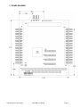
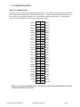
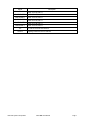
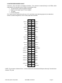
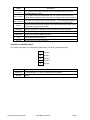
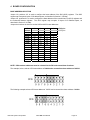
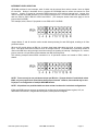
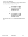
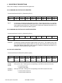
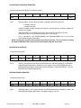
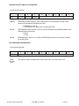
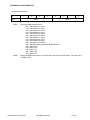
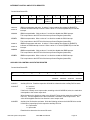
GPIO-MM
FPGA-based PC/104
Counter/Timer and Digital I/O Module
USER MANUAL V1.00
© Copyright 2006
Diamond Systems Corporation
1255 Terra Bella Ave.
Mountain View, CA 94043
Tel (650) 810-2500
Fax (650) 810-2525
www.diamondsystems.com
TABLE OF CONTENTS
1
GENERAL DESCRIPTION...........................................................................................................................................3
2
BOARD DRAWING........................................................................................................................................................5
3
I/O CONNECTOR PINOUT ..........................................................................................................................................6
4
BOARD CONFIGURATION .......................................................................................................................................10
5
I/O MAP .........................................................................................................................................................................13
6
REGISTER BIT DESCRIPTIONS ..............................................................................................................................14
7
PROGRAMMING THE COUNTER/TIMER ............................................................................................................22
8
PROGRAMMING DIGITAL I/O................................................................................................................................24
9
PROGRAMMING ENHANCED FEATURES...........................................................................................................26
10
SPECIFICATIONS ...................................................................................................................................................27
11
ADDITIONAL INFORMATION.............................................................................................................................28
Diamond Systems Corporation
GPIO-MM User Manual
Page 2
1 GENERAL DESCRIPTION
The GPIO-MM is a PC/104 board featuring 48 Digital I/O (DIO) lines, 10 16-bit counter/timers, 8 bits of TTL
input, 8 bits of TTL output, and software-controlled interrupt capability. The DIO and counter/timer functions
are implemented in FPGA cores, emulating dual 82C55A PPI and dual CTS9513 counter/timer chips.
A 50-pin I/O header provides for external DIO connections. Direction on all ports is selected by programming
control registers in the FPGA. All I/O lines are buffered with transceivers, whose directions are controlled by
logic that responds to the direction control values written to the registers. Each line is capable of sinking
64mA in a logic low state or sourcing 15mA in a logic high state. The board requires only +5V for operation.
DIO headers are organized to allow direct interfacing to OPTO-22's isolated I/O racks, including the G4
series, the PB16-H, -J, -K, -L, PB8H, and the PB24HQ. These racks and I/O modules allow up to 3000
VRMS isolation between the computer and the user's signals. All control signals, power, and ground on the
DIO header match the corresponding signals on these I/O racks, so a single 50-pin ribbon cable, such as
Diamond Systems' C50-18, is all that is needed to make the connection.
The FPGA counter/timer cores provide an additional 8-bit TTL output port with up to ±4 mA per bit and a
separate 8-bit TTL input port. Both ports can be operated in bit or byte mode.
The counter/timer provides ten extremely versatile counters with a wide variety of features, including up or
down counting, binary or BCD counting, single or repetitive counting, edge or level gating, output pulse or
toggle capability, alarm comparator circuitry, and software or hardware retriggering.
All counter features are programmable through software. In addition, an internal series of frequencies is
provided, which may be used as internal count sources. The counter/timers can be used to generate
retriggerable one-shots, timed pulses, and square waves of variable duty cycle, and to count pulses, measure
time intervals between pulses, and measure the frequency and period of a periodic waveform.
The GPIO-MM provides access to interrupt levels 3-7, 10-12 and 15 on the PC bus for real-time background
applications. Interrupts provide a means for transferring data into or out of PC memory under external
control. Using interrupts allows "background" operation, where I/O can be performed while the PC is
executing another task , such as running an unrelated applications program. This feature is useful for
performing I/O at a controlled rate, since a counter output can be used to drive the interrupt request pin on
the I/O header at a periodic rate for a user-supplied interrupt service routine that performs whatever function
is necessary in response to the interrupt.
DIGITAL I/O FEATURES
♦
Dual 82C55A Parallel Peripheral Interfaces (PPI) logic implemented in FPGA cores.
♦
Each 82C55A has three 8-bit I/O ports for a total of 48 DIO lines, which connect to a 50-pin header for
external connections.
♦
Port direction and operation is selected through software programmable control registers.
♦
All lines are buffered with transceivers.
COUNTER/TIMER FEATURES
♦
Dual CTS9513 counter/timers logic implemented in FPGA cores.
♦
A 40MHz clock input, providing higher precision timer functions.
♦
Ten 16-bit programmable up/down counters with sophisticated timing logic:
♦
Up or down counting.
♦
Binary or BCD counting.
♦
Single or repetitive counting.
♦
Edge or level gating.
♦
Output pulse or toggle capability.
♦
Alarm comparator circuitry.
♦
Software or hardware retriggering.
♦
Timing functions are software programmable, using control registers.
♦
8-bit TTL input and 8-bit TTL output ports, which can operate in bit- or byte mode.
♦
An interrupt line for generating interrupts to the CPU.
Diamond Systems Corporation
GPIO-MM User Manual
Page 3
♦
An external 50-pin header for connecting to the counter/timer features.
ENHANCED FEATURES
♦
On-board EEPROM for user configuration data storage.
♦
An LED display for easy identification of FPGA personality, which can also be read in a register.
♦
Interrupt source selection, with counter/timer, DIO or external line options.
♦
Four-channel auxiliary DIO for additional general-purpose I/O.
♦
A register-accessible FPGA revision code for version control.
♦
Software-controlled board reset.
Diamond Systems Corporation
GPIO-MM User Manual
Page 4
2 BOARD DRAWING
.
Diamond Systems Corporation
GPIO-MM User Manual
Page 5
3
I/O CONNECTOR PINOUT
DIGITAL I/O HEADER PINOUT
Connector (J4) is the 50-pin general-purpose DIO interface. The connector connects directly to the FPGA,
which implements the functionality of two 82C55A PPI chips. This gives a total of 48 bidirectional DIO lines.
The J4 pins can be configured to pull-up to +5V or pull-down to ground using jumper J11, as described in
Section 4, Board Configuration, I/O Line Pull-up/pull-down Selection.
DIOA7
1
2
DIOD7
DIOA6
3
4
DIOD6
DIOA5
5
6
DIOD5
DIOA4
7
8
DIOD4
DIOA3
9
10
DIOD3
DIOA2
11
12
DIOD2
DIOA1
13
14
DIOD1
DIOA0
15
16
DIOD0
DIOC7
17
18
DIOF6
DIOC6
19
20
DIOF6
DIOC5
21
22
DIOF5
DIOC4
23
24
DIOF4
DIOC3
25
26
DIOF3
DIOC2
27
28
DIOF2
DIOC1
29
30
DIOF1
DIOC0
31
32
DIOF0
DIOB7
33
34
DIOE7
DIOB6
35
36
DIOE6
DIOB5
37
38
DIOE5
DIOB4
39
40
DIOE4
DIOB3
41
42
DIOE3
DIOB2
43
44
DIOE2
DIOB1
45
46
DIOE1
DIOB0
47
48
DIOE0
+5V
49
50
Ground
NOTE: The connector is labeled “Port 2,” which should not be confused with DIO ports A, B and
C and the fixed-direction TTL ports.
Diamond Systems Corporation
GPIO-MM User Manual
Page 6
Signal
DIOA0-DIOA7
8255-1 Port A, bits 0-7
DIOB0-DIOB7
8255-1 Port B, bits 0-7
DIOC0-DIOC7
8255-1 Port C, bits 0-7
DIOD0-DIOD7
8255-2 Port A, bits 0-7
DIOE0-DIOE7
8255-2 Port B, bits 0-7
DIOF0-DIOF7
8255-1 Port C, bits 0-7
+5V
Ground
Diamond Systems Corporation
Description
+5 volt DC from the PC/104 bus.
Digital ground from the PC/104 bus.
GPIO-MM User Manual
Page 7
COUNTER/TIMER HEADER PINOUT
Connector (J3) is the 50-pin counter/timer interface. The connector connects directly to the FPGA, which
implements the functionality of two CTS9513 counter/timer chips.
♦
♦
♦
♦
Ten input and ten output counter/timer signals
Eight input and eight output TTL-level signals
Ten gates
Power and ground
The J3 pins may be configured to pull-up to +5V or pull-down to ground using jumper J8, as describe in
Section 4, Board Configuration, I/O Line Pull-up/pull-down Selection.
In 1
1
2
In 2
Gate 1
3
4
Gate 2
Out 1
5
6
Out 2
In 3
7
8
In 4
Gate 3
9
10
Gate 4
Out 3
11
12
Out 4
In 5
13
14
Out 5
Gate 5
15
16
FOUT
In 6
17
18
In 7
Gate 6
19
20
Gate 7
Out 6
21
22
Out 7
In 8
23
24
In 9
Gate 8
25
26
Gate 9
Out 8
27
28
Out 9
In 10
29
30
Out 10
Gate 10
31
32
Interrupt In
DOUT7
33
34
DIN7
DOUT6
35
36
DIN6
DOUT5
37
38
DIN5
DOUT4
39
40
DIN4
DOUT3
41
42
DIN3
DOUT2
43
44
DIN2
DOUT1
45
46
DIN1
DOUT0
47
48
DIN0
+5V
49
50
Ground
NOTE: The connector is labeled “Port 1,” which should not be confused with DIO ports A through F and the fixeddirection TTL ports.
Diamond Systems Corporation
GPIO-MM User Manual
Page 8
Signal
In 1-In 10
Description
Ten external clock source lines that may be associated with one of the ten
internal counters or FOUT..
Out 1-Out 10
Ten tri-state outputs lines associated with one of the ten internal counters.
These may be programmed for pulse, wave or complex duty cycle waveforms.
Gate 1-Gate 10
Ten input lines used to control counter behavior. These may also be used as
clock or count input sources for the internal counters or the FOUT divider.
FOUT
FOUT is a general-purpose, auxiliary clock output derived from the 9513 input
clock using a programmable divider.
Interrupt In
DOUT0-OUT7
DIN0-DIN7
+5V
Ground
External interrupt for external PC/104 bus hardware interrupt operation.
Eight general-purpose digital output lines.
Eight general-purpose digital input lines.
+5 volt DC from the PC/104 bus.
Digital ground from the PC/104 bus.
AUXILIARY I/O HEADER PINOUT
The auxiliary I/O header (J5) is provided for bidirectional, TTL-level, general-purpose I/O.
Signal
AuxI/O 0-3
Ground
1
AuxI/O 0
2
AuxI/O 1
3
AuxI/O 2
4
AuxI/O 3
5
Ground
Description
Four bidirectional, TTL-level, general-purpose I/O signals
ground
Diamond Systems Corporation
GPIO-MM User Manual
Page 9
4 BOARD CONFIGURATION
BASE ADDRESS SELECTION
Jumper J10, positions 2-5, is used to configure the base address of the DIO (8255) registers. The 8255
register map occupies 8 bytes of I/O address space, as described in Section 5, I/O Map.
Jumper J10, positions 6-9, is used to configure the base address of the counter/timer I/O (9513) registers and
the enhanced features registers. The 9513 register map occupies 16 bytes of I/O address space, as
described in Section 5, I/O Map.
Jumper the locations as shown to set the 8255 and 9513 base addresses.
I/O
Address
0040h
0080h
00C0h
0100h
0140h
0180h
01C0h
0200h
0240h
0280h
02C0h
0300h
0340h
0380h
03C0h
2
6
3
7
4
8
5
9
Out
In
In
In
In
Out
In
In
Out
Out
In
In
In
In
Out
In
Out
In
Out
In
In
In
Out
Out
Out
Out
Out
In
In
In
In
Out
Out
In
In
Out
In
Out
In
Out
Out
Out
In
Out
In
In
Out
Out
Out
In
Out
Out
In
Out
Out
Out
Out
Out
Out
Out
◄ DIO pins
◄ C/T pins
NOTE: Different base addresses must be selected for the DIO and counter/timer functions.
The example, below, selects a DIO base address of 0040h and a counter/timer base address of 03C0H.
The following example selects a DIO base address of 03C0H and a counter/timer base address of 0100h.
Diamond Systems Corporation
GPIO-MM User Manual
Page 10
INTERRUPT LEVEL SELECTION
GPIO-MM provides for two interrupts, each of which may be sourced from various counter / timer or digitial
I/O functions. Section 6 describes how to program the GPIO-MM board to select the sources for each
interrupt. Jumper J7 is used to connect the IRQA interrupt to a PC/104 bus interrupt level. Jumper J9 is
used to connect the IRQB interrupt to a PC/104 bus interrupt level. PC/104 lines that can be selected for
each are IRQ3 to IRQ7, IRQ10 to IRQ12 and IRQ15. (The examples shown below also apply to the J9
jumper block for IRQB).
The example, below, shows J7 jumpered to route IRQA to PC/104 IRQ5.
Jumper blocks J7 and J9 are also used to enable interrupt sharing for each IRQ signal, enabling a 1K Ohm
pull-down resistor.
When an I/O module drives an IRQ line, its output signal must either drive logic high, or become a tri-state
input. This allows more than one device to be on a single IRQ line. To facilitate this, a pull-down resistor is
used on the IRQ line to bring the logic low when no device is signaling an interrupt. Shorting the “R,” resistor,
jumper connects a 1K pull-down resistor between the IRQ line and ground.
The following example shows IRQA connected to a 1K pull-down resistor and routed to IRQ5, which is
shared.
NOTE: There can only be one pull-down resistor per IRQ line. If jumper blocks J7 and J9 both select
IRQ5, only one jumper block should have the R-jumper inserted. Likewise, there should only be one
R-jumper in a configuration of multiple GPIO-MM boards.
NOTE: All positions are paralleled with zero-ohm resistor locations for hard-wired configurations.
IRQA and IRQB interrupts sources are selected by configuring the enhanced feature register, 0Ch, as
described in the Section 6, Register Bit Descriptions, Interrupt Source Register.
Diamond Systems Corporation
GPIO-MM User Manual
Page 11
I/O LINE PULL-UP/PULL-DOWN SELECTION
Use jumper J8 to configure the pull-up and pull-down state of the counter/timer header pins (J3). Use jumper
J11 to configure the pull-up and pull-down state of the DIO header pins (J4).
DIO pin pull-up and pull-down state is configured as shown in the following examples.
Jumper the position marked “+5” to pull the J3 I/O pins up to +5VDC.
Jumper the position marked “G” to pull the J3 I/O pins down to ground.
NOTE: Placing a jumper on both “+5” and “G” simultaneously will short the +5VDC power plane to
ground.
Diamond Systems Corporation
GPIO-MM User Manual
Page 12
5 I/O MAP
The register base address for DIO and counter / timer functions is determined by setting jumper J10, as
described in Section 4, Board Configuration, Base Address Selection. Jumper pins 2-5 set the DIO base
address and pins 6-9 set the counter/timer base address.
The following sixteen registers are used for counter/timer and enhanced feature programming.
Offset
Description
00h
9513-1 command and status data register. Transfers command and status data to/from the
register pointed to at base+01h.
01h
9513-1 command and status data register pointer. Address of the command and status
registers for transferring the 8-bit data located at base+00h.
02h
8-bit DIO data. Set or read the 9513 DIO lines.
03h
Shadow register of base+02h.
04h
9513-2 command and status data register. Transfers command and status data to/from the
register pointed to at base+05h.
05h
9513-2 command and status data register pointer. Address of the command and status
registers for transferring the 8-bit data located at base+04h.
06h
Interrupt control. Enable and reset counter/timer interrupts.
07h
Shadow register of base+06h.
08h
EEPROM data. Data written to and read from the EEPROM.
09h
EEPROM address. The EEPROM location for reading or writing data.
0Ah
EEPROM control and status register. Initiate EEPROM data transfer and set the data transfer
direction. Also, indicates when valid data is available from EEPROM during a read operation.
0Bh
FPGA revision code. Get the on-board FPGA program revision level.
0Ch
Interrupt source selection. Specify the interrupt source for IRQA/IRQB.
0Dh
Interrupt control and status. Enable, disable and clear IRQA/IRQB interrupts and gets the
IRQA/IRQB interrupt status.
0Eh
Auxiliary DIO control and status. Set the state of the auxiliary DIO lines and read the current
DIO line state.
0Fh
Board reset and board ID code. Reset the board or get the FPGA personality ID code.
The following eight registers are used for DIO programming.
Offset
Description
00h
8255-1 port A DIO register
01h
8255-1 port B DIO register
02h
8255-1 port C DIO register
03h
8255-1 control and status register
04h
8255-2 port A DIO register
05h
8255-2 port B DIO register
06h
8255-2 port C DIO register
07h
8255-2 control and status register
Diamond Systems Corporation
GPIO-MM User Manual
Page 13
6 REGISTER BIT DESCRIPTIONS
Refer to the I/O Map for counter/timer and DIO register sets.
9513 COMMAND AND STATUS DATA REGISTERS
Counter/timer Base+00h (9513-1), Base+04h (9513-2)
Bit:
Name:
D0-D7
7
6
5
4
3
2
1
0
D7
D6
D5
D4
D3
D2
D1
D0
Counter/timer command and status data for the 9513. These data are written to or read from
the counter/timer command and status register at the location specified by the command and
status register pointer (base+01h). Refer to the 9513 data sheet, Additional Information, for a
description of the command and status registers.
9513 COMMAND AND STATUS DATA POINTER REGISTERS
Counter/timer Base+01h (9513-1), Base+05h (9513-2)
Bit:
7
6
5
4
Name:
POINTER
3
2
1
0
POINTER
Counter/timer command and status register pointer for the 9513. This register points to the
9513 command and status register location to write the data contained in the Command and
Status Data Register (base+00h). Refer to the 9513 datasheet, Additional Information, for a
description of the command and status register.
9513 DIO DATA REGISTERS
Counter/timer Base+02h, Base+03h (shadow register)
Bit:
Name:
7
6
5
4
3
2
1
0
DIO7IN
DIO6IN
DIO5IN
DIO4IN
DIO3IN
DIO2IN
DIO1IN
DIO0IN
DIO7OUT
DIO6OUT
DIO5OUT
DIO4OUT
DIO3OUT
DIO2OUT
DIO1OUT
DIO0OUT
DIO0INDIO7IN
DIO input line state. Reading the bit corresponding to the DIO line returns the line state.
DIO0OUTDIO7OUT
DIO output line state. Writing the bit corresponding to the DIO line sets the line state.
0 = low level line state
1 = high level line state
0 = set line state to low level
1 = set line state to high level
Diamond Systems Corporation
GPIO-MM User Manual
Page 14
9513 INTERRUPT CONTROL REGISTERS
Counter/timer Base+06h, Base+07h (shadow register)
Bit:
7
6
5
Name:
INTE
4
3
2
1
0
–
INTE
Interrupt enable. Write to this bit to enable or disable counter/timer interrupts.
0 = disable interrupts
1 = enable interrupts
If IRQA and IRQB are both counter/timer interrupts, both interrupts are enabled or disabled by
writing to this register.
IRQA and IRQB are considered counter/timer interrupts if the interrupt source is the
counter/timer output 1-10, dedicated interrupt input, or DIO input 0.
This is equivalent to the IRQAEN/IRQBEN and IRQADIS/IRQBDIS bits of the Interrupt
Control/Status Register (base+0Dh).
NOTE: Reading this register resets pending counter/timer interrupts. This is equivalent to setting
the IRQACLR/IRQBCLR bits of the Interrupt Control/Status Register (base+0Dh).
EEPROM DATA REGISTER
Counter/timer Base+08h
Bit:
Name:
D0-D7
7
6
5
4
3
2
1
0
D7
D6
D5
D4
D3
D2
D1
D0
Writing to this register writes data to the EEPROM at the address specified by the EEPROM
Address Register (base+09h). Reading from this register returns the EEPROM data at the
EEPROM Address Register (base+09h) location; read data is valid when EEBUSY = 0 in the
EEPROM Status Register (base+0Ah).
EEPROM ADDRESS REGISTER
Counter/timer Base+09h
Bit:
Name:
A0-A7
7
6
5
4
3
2
1
0
A7
A6
A5
A4
A3
A2
A1
A0
EEPROM address. This register specifies the EEPROM address to read/write the data in the
EEPROM Data Register (base+08h). The address range is 0 to 256.
Diamond Systems Corporation
GPIO-MM User Manual
Page 15
EEPROM CONTROL AND STATUS REGISTER
Counter/timer Base+0Ah
Bit:
Name:
EEBUSY
7
6
5
EE_EN
EE_RW
EEBUSY
4
3
2
1
0
EEPROM busy status indicator. When reading data from the EEPROM, the data is valid
when this bit indicates the EEPROM is not busy.
0 = EEPROM is not busy.
1 = EEPROM is busy. Wait before accessing EEPROM.
EE_RW
EEPROM data transfer direction. Read or write the EEPROM at the EEPROM address in the
Address Register (base+09h).
0 = Write
1 = Read
EE_EN
EEPROM enable. Set bit to 1 to initiate an EEPROM byte transfer in the direction indicated
by the EE_RW bit.
FPGA REVISION CODE REGISTER
Counter/timer Base+0Bh
Bit:
7
Name:
FPGA
Revision
Code
6
5
4
3
2
1
0
FPGA Revision Code
This register contains a hexadecimal FPGA revision code. The initial value is 10h.
Diamond Systems Corporation
GPIO-MM User Manual
Page 16
INTERRUPT SOURCE REGISTER
Counter/timer Base+0Ch
Bit:
7
Name:
6
5
4
3
IRQB
2
1
0
IRQA
IRQA
Select the IRQA interrupt source:
00h = Counter/timer 1 output
01h = Counter/timer 2 output
02h = Counter/timer 3 output
03h = Counter/timer 4 output
04h = Counter/timer 5 output
05h = Counter/timer 6 output
06h = Counter/timer 7 output
07h = Counter/timer 8 output
08h = Counter/timer 9 output
09h = Counter/timer 10 output
0Ah = dedicated interrupt input pin ◄ (Reset value)
0Bh = DIO input 0
0Ch = 8255-1 C0
0Dh = 8255-1 C3
0Eh = 8255-2 C0
0Fh = 8255-2 C3
IRQB
Select the IRQA interrupt source, using the same values as for IRQA, above. The reset value
for IRQB is 0Ch.
Diamond Systems Corporation
GPIO-MM User Manual
Page 17
INTERRUPT CONTROL AND STATUS REGISTER
Counter/timer Base+0Dh
Bit:
7
6
5
4
3
2
1
0
Name:
–
IRQBEN
IRQBDIS
IRQBCLR
–
IRQAEN
IRQADIS
IRQACLR
IRQBSTS
IRQASTS
IRQACLR
IRQA interrupt status and reset. A value of 1 when reading this register bit (IRQASTS)
indicates an IRQA interrupt occurred. Write a value of 1 to this bit (IRQACLR) to clear the
interrupt.
IRQADIS
IRQA interrupt disable. Write a value of 1 to this bit to disable the IRQA interrupt.
IRQASTS
This is equivalent to the INTE bit of the Interrupt Control Register (base+0Dh).
IRQAEN
IRQA interrupt enable. Write a value of 1 to this bit to enable the IRQA interrupt.
This is equivalent to the INTE bit of the Interrupt Control Register (base+0Dh).
IRQBSTS
IRQBCLR
IRQB interrupt status and reset. A value of 1 when reading this register bit (IRQBSTS)
indicates an IRQB interrupt occurred. Write a value of 1 to this bit (IRQBCLR) to clear the
interrupt.
IRQBDIS
IRQB interrupt disable. Write a value of 1 to this bit to disable the IRQB interrupt.
This is equivalent to the INTE bit of the Interrupt Control Register (base+0Dh).
IRQBEN
IRQB interrupt enable. Write a value of 1 to this bit to enable the IRQB interrupt.
This is equivalent to the INTE bit of the Interrupt Control Register (base+0Dh).
AUXILIARY DIO CONTROL AND STATUS REGISTER
Counter/timer Base+0Eh
Bit:
Name:
AUXnIN /
7
6
5
4
3
2
1
0
AUX3DIR
AUX2DIR
AUX1DIR
AUX0DIR
AUX3IN
AUX2IN
AUX1IN
AUX0IN
AUX3OUT
AUX2OUT
AUX1OUT
AUX0OUT
Auxiliary DIO line. Read the respective AUXnIN bit to determine the auxiliary DIO line state.
AUXnOUT
0 = low level
1 = high level
If the line is currently set to output mode, according to the AUXnDIR bit, below, the read value
corresponds to the current output level.
Write the low-level or high-level value to the AUXnOUT bit to set the respective auxiliary DIO
line level. The level applies even if the line direction, AUXnDIR, is set to input mode. The
value will be applied when the line direction is set to output mode.
AUXnDIR
Auxiliary line I/O direction and state. Write the following values to the AUXnDIR bit to set the
I/O direction (output/input) for the respective auxiliary DIO line.
0 = output mode
1 = input mode
Read the bit to determine the current I/O mode.
Diamond Systems Corporation
GPIO-MM User Manual
Page 18
BOARD RESET AND ID REGISTER
Counter/timer Base+0Fh
Bit:
Name:
7
6
5
4
3
2
1
0
ID7
ID6
ID5
ID4
ID3
ID2
ID1
ID0
BRDRST
ID0-ID7
FPGA personality ID. Indicates the personality of the onboard FPGA; the value for the
GPIO-MM board type is 11h.
BRDRST
Board reset. Write 1 to this bit to reset the board, which has the same affect as an
external reset pulse.
8255 DATA REGISTERS
DIO Base+00h (8255-1 Port A), DIO Base+04h (8255-2 Port A)
DIO Base+01h (8255-1 Port B), DIO Base+05h (8255-2 Port B)
DIO Base+02h (8255-1 Port C), DIO Base+06h (8255-2 Port C)
Bit:
7
6
5
4
3
2
1
0
Name:
DATA
DATA
8-bit parallel data. On reset, the port is set to input mode and the port is held at a logic
level 1 until the reset signal is removed. The port remains in input mode until changed
using the control register.
Following a reset, all lines are set to input mode.
Diamond Systems Corporation
GPIO-MM User Manual
Page 19
8255 CONTROL AND STATUS REGISTERS (BASIC MODE DEFINITION – MSFLAG=1)
DIO Base+03h (8255-1), DIO Base+07h (8255-2)
Bit:
7
6
5
MSELA
4
3
2
1
0
PADIR
PCUDIR
MSELB
PBDIR
PCLDIR
Name:
MSFLAG
PCLDIR
Port C (lower) direction. Sets the direction of the port C I/O signals 0-3.
0 = output
1 = input ◄ (Reset value)
PBDIR
Port B direction. Sets the direction of the port B I/O signals.
0 = output
1 = input ◄ (Reset value)
MSELB
Group B mode selection. Sets the mode of operation for the group B signals.
0 = mode 0 ◄ (Reset value)
1 = mode 1
NOTE: 1. Only mode 0 is currently implemented.
2. All output registers are reset when the mode is changed.
PCUDIR
Port C (upper) direction. Sets the direction of the port C I/O signals 4-7.
0 = output
1 = input ◄ (Reset value)
PADIR
Port A direction Sets the direction of the port A I/O signals.
0 = output
1 = input ◄ (Reset value)
MSELA
Group A mode selection. Sets the mode of operation for the group B signals.
00h = mode 0 ◄ (Reset value)
01h = mode 1
1xh = mode
NOTE: 1. Only mode 0 is currently implemented.
2. All output registers are reset when the mode is changed.
MSFLAG
Mode set flag. Selects the port configuration mode.
0 = Bit set/reset control register mode
When MSFLAG is reset, this register is used to set/reset individual Port C
Bits.
1 = Basic mode definition control register mode ◄ (Reset value)
When MSFLAG is set, this register is used for direction and mode selection.
NOTE: When the control word is read, the value of MSFLAG is always 1, implying basic
control word information is being read.
Diamond Systems Corporation
GPIO-MM User Manual
Page 20
8255 CONTROL AND STATUS REGISTERS (BIT SET/RESET MODE – MSFLAG=0)
DIO Base+03h (8255-1), DIO Base+07h (8255-2)
Bit:
7
6
5
Name:
MSFLAG
SET
Bit set/reset individual command.
4
3
–
2
BSEL
1
0
SET
0 = reset
1 = set
BSEL
Port C bit select.
0 = bit 0
1 = bit 1
2 = bit 2
3 = bit 3
4 = bit 4
5 = bit 5
6 = bit 6
7 = bit 7
MSFLAG
Mode set flag. Selects the port configuration mode.
0 = Bit set/reset control register mode
When MSFLAG is reset, this register is used to set/reset individual Port C
Bits.
1 = Basic mode definition control register mode
When MSFLAG is set, this register is used for direction and mode selection.
NOTE: When the control word is read, the value of MSFLAG is always 1, implying basic
control word information is being read.
Diamond Systems Corporation
GPIO-MM User Manual
Page 21
7 PROGRAMMING THE COUNTER/TIMER
To program the 9513 effectively and take advantage of its myriad of features requires an understanding of its
structure and operation. A datasheet on the 9513 is included at the end of this manual.
Review pages 4 (starting with “Functional Description”) through 11 to understand the structure of the 9513
chip and its capabilities. The various counter operating modes are described starting on page 13. A few
explanatory notes are given below.
ACCESSING THE COUNTER/TIMER INTERNAL REGISTERS
The chip contains many internal registers. To minimize the I/O memory footprint, a data pointer scheme is
used to access these registers. This scheme is reflected in the GPIO-MM board’s I/O map (Section 5, I/O
Map). The data pointer values are shown in the 9513 datasheet on page 8, Table 4. The appropriate data
pointer value is written to the data pointer register for the chip (Base + 1 for chip no. 1 and Base + 5 for chip
no. 2). Then the register is accessed through the data register (Base + 0 for chip no. 1 and Base + 4 for chip
no. 2).
MASTER MODE REGISTER
Each chip contains a Master Mode Register that defines global characteristics for the chip. Note the bit that
controls the data bus width. This should always be set to 0 for 8-bit bus access on GPIO-MM.
COUNTER MODE REGISTER
Each chip contains five Counter Mode Registers; one for each counter. This register is used to program the
operating mode of the counter, including input source, gating method, output type, load/reload behavior and
count direction. Note that in the Gate description, Gate N means the gate for the counter being programmed,
and Gate N-1 means the gate for the previous counter. Gate N-1 is not valid for counter 1 (or counter 6 on
GPIO-MM, since that corresponds to counter 1 on the second chip).
COUNTER MODES
Each combination of Gate control, Repetition, Reload source, and Special gate are given a letter mode name.
See the counter mode tables on page 13 of the datasheet. The behavior of these modes as well as their
timing diagrams are given starting on page 14 of the datasheet. Please, note the errata on page 12 of the
datasheet.
FOUT FREQUENCY OUTPUT
A programmable frequency generator circuit is provided for the counter/timer, and is described in the 9513
datasheet. It has an input source, a multi-stage decimal or BCD divider, and a user-programmable divider.
All options are programmed through the Master Mode Register. The FOUT circuit of the 9513-1 is available
on the FOUT pin on the GPIO-MM board’s I/O header. Its source can be the input or gate from counters 1-5
or any of the five internal frequency dividers built into the chip and driven by the clock. The FOUT circuit of
the 9513-2 is not available externally.
COUNTER COMMANDS
A set of commands is used to control the counters. These are described in the 9513 datasheet. The
Diamond Systems Universal Driver software provides full support for the various 9513 functions.
COUNTER PROGRAMMING
Before programming any individual counter, the 9513 Master Mode Register must be programmed.
Programming an individual counter requires several steps. First, the Counter Mode Register must be set to
indicate the desired operating characteristics of the counter, such as gating level and type, count direction
and type, and output type.
After the Counter Mode Register is programmed, load the appropriate data into the Load and/or Hold
register(s). The Load register is used to set the divide-by-n and initial count values. The Hold register may
also be required for certain counter modes, such as variable-duty-cycle square wave functions.
Diamond Systems Corporation
GPIO-MM User Manual
Page 22
You may optionally want to set the initial output level.
If you are using counters 1 or 2 in alarm mode, the alarm register must also be programmed.
Next, load the initial count into the Count register using the Load command.
Finally, "arm", or enable, the counter using the Arm command.
To read a counter, issue a Save command. This stores the counter’s current contents in the Hold register.
Then, read the Hold register.
A counter can be armed or disarmed, and its current contents can be saved, at any time under software
control through these commands.
The information below summarizes the procedure for programming a counter:
To set up counter operation:
1. Program the Master Mode Register
2. Program the Counter Mode Register
3. Load initial data into the Load register
4. (Optional) Load initial data into the Hold register
5. Issue a Load and Arm command for the counter
To read counter contents:
1. Issue a Save or Disarm and Save command
2. Read the Hold register
Diamond Systems Corporation
GPIO-MM User Manual
Page 23
8 PROGRAMMING DIGITAL I/O
48-BIT PROGRAMMABLE DIRECTION (8255)
GPIO-MM provides 48 DIO lines using an FPGA core implementation of two 82C55A devices (82C55A-1 and
82C55A-2). The DIO functionality includes 48 programmable direction lines, and 8 fixed inputs and 8 fixed
outputs. The 48 programmable I/O lines are buffered for enhanced output current, while the fixed I/O and the
counter/timer signals feature ESD-protective circuitry. All I/O lines contain jumper-selectable 10Kohm pullup/pull-down resistors.
Operation of the 82C55A FPGA core should be as described in the 82C55A PPI datasheet. Refer to the
82C55A datasheet, Additional Information, for detailed register and programming information.
The 82C55A has three parallel I/O ports. Ports A and B are 8-bit bi-directional I/O ports. Port C is divided
into two 4-bit bi-directional I/O ports. For programming, the ports are arranged into two groups, as shown
below.
Port Group
Description
A
8 bits of Port A and upper 4 bits (4-7) of port
C.
B
8 bits of Port B and lower 4 bits (0-3) of port C.
NOTE: The port groups can be separately configured for different operating modes. However, GPIOMM only implements operating mode 0, which provides simple, bidirectional I/O without handshaking.
Port C bits may be individually set and reset by setting the MSFLAG in the 8255 Control and Status Register
and programming the remaining register bits for the desired bit state.
Setting the 8255 Control and Status Register to the following values gives 16 possible I/O configurations.
Status and Control Register Bits
Group A
Group B
PADIR
PCUDI
R
PBDIR
PCLDIR
Port A
Port C
(upper)
Port B
Port C
(lower)
0
0
0
0
Output
Output
Output
Output
0
0
0
1
Output
Output
Output
Input
0
0
1
0
Output
Output
Input
Output
0
0
1
1
Output
Output
Input
Input
0
1
0
0
Output
Input
Output
Output
0
1
0
1
Output
Input
Output
Input
0
1
1
0
Output
Input
Input
Output
0
1
1
1
Output
Input
Input
Input
1
0
0
0
Input
Output
Output
Output
1
0
0
1
Input
Output
Output
Input
1
0
1
0
Input
Output
Input
Output
1
0
1
1
Input
Output
Input
Input
1
1
0
0
Input
Input
Output
Output
1
1
0
1
Input
Input
Output
Input
1
1
1
0
Input
Input
Input
Output
1
1
1
1
Input
Input
Input
Input
Diamond Systems Corporation
GPIO-MM User Manual
Page 24
16-BIT FIXED DIRECTION (9513)
Connector J3 has 8 fixed TTL inputs and 8 fixed TTL outputs. The outputs are set by writing to the register at
counter/timer base+2 or 3. (See 9513 DIO Data Registers). Write an 8-bit value to the register at base+2 (or
base+3) to immediately output the value to the 8 output lines. When reading register base+2 (or base+3), the
FPGA returns the logic state of the 8 input lines.
Diamond Systems Corporation
GPIO-MM User Manual
Page 25
9 PROGRAMMING ENHANCED FEATURES
EEPROM PROGRAMMING
The EEPROM provides non-volatile memory for storing application data.
Program the EEPROM using the following steps. Repeat these steps for each data byte.
1. Write the data byte to the EEPROM Data Register (08h).
2. Specify the EEPROM address (0-256) where the data is to be written by writing the address to the
EEPROM Address Register (09h).
3. Set the data transfer direction to write by resetting the EE_RW bit in the EEPROM Control and Status
Register (0Ah).
4.
Set the EE_EN bit in the EEPROM Control and Status Register (0Ah) to initiate the write operation.
To read stored EEPROM data, use the following steps. Repeat these steps for each data byte.
1. Specify the EEPROM address (0-256) where the data is to be read from by writing the address to the
EEPROM Address Register (09h).
2. Set the data transfer direction to read by setting the EE_RW bit in the EEPROM Control and Status
Register (0Ah).
3. Reset the EE_EN bit in the EEPROM Control and Status Register (0Ah) to initiate the read operation.
4. Test the EEPROM Control and Status Register (0Ah) EEBUSY bit to determine that the data transfer
has completed. When EEBUSY is zero, a valid data byte is available and the next byte may be read.
Diamond Systems Corporation
GPIO-MM User Manual
Page 26
10 SPECIFICATIONS
Base FPGA
Input clock
FPGA code storage
ID indicator
Counter/timers
Maximum counting frequency
Counter modes
Programmable I/O
Fixed direction I/O
Output current, buffered I/O
Output current, fixed I/O and counter/ timers
Dimensions
PC/104 bus
Power supply
Operating temperature
Weight
Xilinx Spartan II, 200,000 gates, 40K RAM
bits
40MHz
Flash memory, field upgradeable via JTAG
8-bit LED display indicates FPGA code
personality; field upgradeable via JTAG
10, 16 bits, using 2 CTS9513 cores
40MHz
Counter, rate/square-wave generator, pulsewidth modulator, programmable one-shot,
hardware/software triggered strobe
48, using 2 82C55A cores
8 fixed inputs, 8 fixed outputs
Logic 0: 64mA max per line buffered I/O
Logic 1: -15mA max per line
±24mA max
3.55" x 3.775", PC/104 form factor
16-bit stackthrough ISA bus
+5VDC ±5%
-40° to +85° C
2.2oz
Table 1. GPIO-MM Specifications
Diamond Systems Corporation
GPIO-MM User Manual
Page 27
11 ADDITIONAL INFORMATION
Datasheets are provides as a programming reference for the counter/timer and DIO functions.
•
CTS9513-2 5Chan 16 bit 20MHz Counter/Timer, Celeritous Technical Services Corp., September 2000
•
82C55A CMOS Programmable Peripheral Interface, Harris Semiconductor, March 1997
Diamond Systems Corporation
GPIO-MM User Manual
Page 28