1
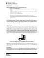
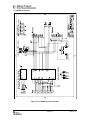
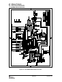
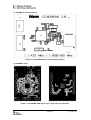
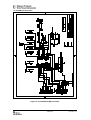
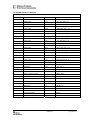
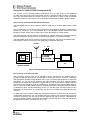
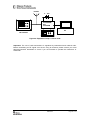
User Manual
Rev. 2.0
CC1020/1070DK Development Kit
SWRU052
Table of Contents:
INTRODUCTION ....................................................................................................................... 3
CC1020/1070DK DEVELOPMENT KIT CONTENTS............................................................... 4
CC1020EB EVALUATION BOARD.......................................................................................... 5
DESCRIPTION ........................................................................................................................... 5
VOLTAGE SUPPLY ..................................................................................................................... 5
PC-INTERFACE ......................................................................................................................... 5
CC1020EB SCHEMATICS ......................................................................................................... 6
CC1020EB BILL OF MATERIALS ............................................................................................... 9
CC1020EB LAYOUT .............................................................................................................. 12
CC1020EMX AND CC1070EM EVALUATION MODULES ................................................... 13
DESCRIPTION ......................................................................................................................... 13
CC1020EMX-433 SCHEMATIC .............................................................................................. 18
CC1020EMX-433 BILL OF MATERIALS ................................................................................... 19
CC1020EMX-868/915 SCHEMATIC ....................................................................................... 21
CC1020EMX-868/915 BILL OF MATERIALS ............................................................................ 22
CC1020EMX ASSEMBLY DRAWINGS ...................................................................................... 24
CC1020EMX LAYOUT ........................................................................................................... 24
CC1070EM-433 SCHEMATIC ................................................................................................. 25
CC1070EM-433 BILL OF MATERIALS ..................................................................................... 26
CC1070EM-868/915 SCHEMATIC .......................................................................................... 27
CC1070EM-868/915 BILL OF MATERIALS ............................................................................... 28
C1070EM ASSEMBLY DRAWINGS ........................................................................................... 29
CC1070EM LAYOUT .............................................................................................................. 29
USING THE CC1020/1070DK DEVELOPMENT KIT ............................................................. 30
HOW TO SET UP A TRANSMITTER (CC1020 AND CC1070)........................................................ 30
HOW TO SET UP A RECEIVER (CC1020)................................................................................... 30
GENERAL INFORMATION..................................................................................................... 32
ADDRESS INFORMATION..................................................................................................... 33
SWRU052
Page 2 of 33
Introduction
The CC1020 single chip transceiver and the CC1070 single chip transmitter provide
extensive features and great flexibility, which make the chips suitable for a very large number
of applications and system requirements. The CC1020 and CC1070 are especially suited for
narrowband systems. The CC1020/1070DK development kit is primarily designed to make it
easy for designers to evaluate transceiver and transmitter performance and in a minimum of
time develop their own applications.
The CC1020/1070DK development kit includes two CC1020EB evaluation boards, two
CC1020EMX evaluation modules and one CC1070EM evaluation module. The CC1020EMX
includes the CC1020 transceiver chip with the external components necessary for operation.
The CC1070EM includes the CC1070 transmitter chip with the external components
necessary for operation. The evaluation modules are mounted onto the CC1020EB, which is
equipped with a voltage regulator and a PC interface circuitry. Using the CC1020EB
connected to a PC running the SmartRF® Studio software, various CC1020 and CC1070
system parameters can be changed and tested.
Technical features:
CC1020 :
-
RF output power up to +10/+5 dBm programmable in 1 dB steps at 433/868 MHz
respectively
-
High sensitivity (up to –121 dBm for a 12.5 kHz channel)
-
Low Adjacent Channel Power (ACP)
-
High Adjacent Channel Rejection (ACR)
-
Integrated bit synchronizer
-
Image rejection mixer
-
Automatic Frequency Control which reduces the crystal accuracy requirement
-
Digital RSSI and carrier sense indicator
CC1070 :
-
RF output power up to +10/+8 dBm programmable in 1 dB steps at 433/868 MHz
respectively
-
Low Adjacent Channel Power (ACP)
This user manual describes how to get started with the CC1020/1070DK development kit.
You will also find description on the CC1020EB, CC1020EMX, CC1070EM and advice on
how to develop your own applications. For details on CC1020 and CC1070 please refer to the
corresponding data sheet. For details on how to use the SmartRF® Studio software please
refer to the SmartRF® Studio user manual.
SWRU052
Page 3 of 33
CC1020/1070DK Development Kit Contents
Your SmartRF® CC1020/1070DK development kit should contain the following items:
Item
Quantity
Comment
CC1020EB evaluation board
2
CC1020EMX evaluation module
2
CC1070EM evaluation module
1
PC parallel port extension cable
2
Adapter
6
25-pin D-sub, male-female, 3 m
Antenna
2
SMA male- BNC female
CC1020 samples
5
50Ω, λ/4 monopole, SMA male
CC1070 samples
5
CC1020/1070 Quick Start User Manual
1
SWRU052
Page 4 of 33
CC1020EB Evaluation Board
The CC1020EB evaluation board includes the following items:
•
4-10 V to 3 V voltage regulator
•
Possibility to apply a 3 V voltage source directly (chosen by the switch on the
board)
•
Voltage-level interface circuitry between the CC1020 or CC1070 chip (3 V) and the
parallel port of the computer (5 V)
•
Connector for a PC parallel port cable
•
Connectors for modulation data in/out and synchronisation clock output
•
2 x 10 female connectors for connection to CC1020 or CC1070 evaluation module
(described later)
Description
The CC1020EB constitutes of three main parts. These are the sockets for the evaluation
module (RF-section), the voltage supply and the PC-interface. The CC1020EB includes a
number of components for maximum flexibility. However, only a minor part of these
components are required in an actual application. Check the CC1020 and CC1070
datasheets for typical application circuits.
Voltage supply
The user can choose between applying a 4-10 V non-regulated supply voltage or a 3 V
regulated supply voltage by setting a switch on the board (SPDT). If a non-regulated supply
voltage is applied, an on board regulator generates a regulated 3 V supply. A diode prevents
damage if the wrong polarity is used for the non-regulated input. The connector has five
contacts as shown in Figure 1. In addition to the three supply voltage contacts, there are two
contacts, which can be used to measure the CC1020 or CC1070 DC current. A short jumper
is placed between these two contacts for the circuit to work in the default configuration. If you
want to measure the DC current, replace the jumper with an ampere meter as shown in
Figure 1.
4-10 V
GND
3V
I_OUT
A
I_IN
Figure 1: The voltage supply connector with an ampere meter attached
Important: For narrowband applications phase noise is a critical parameter. Make sure your
voltage supply has sufficiently low noise performance so as not to degrade your
measurements.
PC-interface
The PC-interface is a 5-to/from-3 V level shift circuit, which buffers all control lines. The
various CC1020 and CC1070 system parameters can be changed through the PC interface
by running the SmartRF® Studio software.
SWRU052
Page 5 of 33
CC1020EB Schematics
Figure 2. CC1020EB top level schematic
SWRU052
Page 6 of 33
Figure 3. CC1020EB voltage regulator schematic
SWRU052
Page 7 of 33
Figure 4. CC1020EB PC interface schematic
SWRU052
Page 8 of 33
CC1020EB Bill of Materials
Voltage regulator
Reference
Description
Value
Part
C4
Capacitor 1206
2.2 uF
C_2U2_1206_X7R_K_10
C5
Capacitor 1206
2.2 uF
C_2U2_1206_X7R_K_10
C6
Capacitor 0603
10 nF
C_10N_0603_X7R_K_50
C7
Capacitor low ESR
Not used
R3
Resistor 0603
Not used
R30
Resistor 0603
Not used
R31
Resistor 0603
Not used
D1
Diode, Si
BAT254
S1
SPDT switch
SWITCH_SPDT
U1
Voltage regulator
LP2985, 3V, National Semiconductor
PC interface
Reference
Description
Value
Part
C8
Capacitor 0603
33 nF
C_33N_0603 _X7R_K_25
C9
Capacitor 0603
33 nF
C_33N_0603 _X7R_K_25
Q1
BJT, Si, NPN, small signal
BC846
Q2
BJT, Si, NPN, small signal
BC846
Q3
BJT, Si, NPN, small signal
BC846
Q4
BJT, Si, NPN, small signal
BC846
Q5
BJT, Si, NPN, small signal
BC846
R4
Resistor 0603
10 kΩ
R_10K_0603_G
R5
Resistor 0603
10 kΩ
R_10K_0603_G
R6
Resistor 0603
10 kΩ
R_10K_0603_G
R7
Resistor 0603
10 kΩ
R_10K_0603_G
R8
Resistor 0603
10 kΩ
R_10K_0603_G
R9
Resistor 0603
10 kΩ
R_10K_0603_G
R10
Resistor 0603
10 kΩ
R_10K_0603_G
R11
Resistor 0603
10 kΩ
R_10K_0603_G
R12
Resistor 0603
10 kΩ
R_10K_0603_G
R13
Resistor 0603
10 kΩ
R_10K_0603_G
R14
Resistor 0603
10 kΩ
R_10K_0603_G
R15
Resistor 0603
10 kΩ
R_10K_0603_G
R16
Resistor 0603
10 kΩ
R_10K_0603_G
R17
Resistor 0603
10 kΩ
R_10K_0603_G
R18
Resistor 0603
10 kΩ
R_10K_0603_G
R19
Resistor 0603
10 kΩ
R_10K_0603_G
R20
Resistor 0603
10 kΩ
R_10K_0603_G
R21
Resistor 0603
10 kΩ
R_10K_0603_G
R22
Resistor 0603
10 kΩ
R_10K_0603_G
SWRU052
Page 9 of 33
R23
Resistor 0603
10 kΩ
R_10K_0603_G
R24
Resistor 0603
100 kΩ
R_100K_0603_G
R25
Resistor 0603
100 kΩ
R_100K_0603_G
R26
Resistor 0603
100 kΩ
R_100K_0603_G
R27
Resistor 0603
100 kΩ
R_100K_0603_G
R28
Resistor 0603
100 kΩ
R_100K_0603_G
R29
Resistor 0603
Not used
U2
Hex inverter, oc
74HC05
U3
Hex inverter, oc
74HC05
Evaluation board
Reference
Description
Value
Part
C1
Capacitor 1206
2.2 uF
C_2U2_1206_X7R_K_10
C2
Capacitor 0603
220 pF
C_220P_0603_NP0_G_50
C3
Capacitor 0603
33 nF
C_33N_0603_X7R_K_25
R1
Resistor 0603
470 Ω
R_470_0603_J
R2
Resistor 0603
470 Ω
R_470_0603_J
D2
LED, green, SMD
LED_CL150GCD
D3
LED, yellow, SMD
LED_CL150YCD
H1
Circuit Board Support
H2
Circuit Board Support
H3
Circuit Board Support
H4
Circuit Board Support
P1
D-Sub, 25 pin
DSUB_25
P2
5 pin terminal, screw
SCREW_TERM_5
P3
Connector, 0.9mm pin female
CONN10_FEMALE
P4
Connector, 0.9mm pin female
CONN10_FEMALE
P5
SMA connector
SMA_RA (Right angle)
P6
SMA connector
SMA_RA (Right angle)
P7
Pinrow, 2x5
PINROW_2X5
SWRU052
Page 10 of 33
CC1020EB Assembly Drawing
Figure 5. CC1020EB PCB assembly drawing
SWRU052
Page 11 of 33
CC1020EB Layout
Figure 6. CC1020EB PCB layout. Layer 1 (top) and Layer 2 (bottom)
SWRU052
Page 12 of 33
CC1020EMX and CC1070EM Evaluation Modules
The CC1020EMX evaluation module includes the following items:
•
A SmartRF® CC1020 transceiver chip
•
Antenna input/output matching network
•
Connector for antenna (50 Ω SMA)
•
2 x 10 male connectors for connection to CC1020EB evaluation board
The CC1020EMX is distributed in two versions, 433 MHz and 868/915 MHz, and the
difference is the frequency band of operation. The operating frequency band is marked on the
CC1020EMX evaluation module.
•
The 433 MHz CC1020EMX-433 evaluation module is optimised for 12.5/25 kHz
channel spacing
•
The 868/915 MHz CC1020EMX-868 evaluation module is optimised for 25 kHz
channel spacing
The CC1070EM evaluation module includes the following items:
•
A SmartRF® CC1070 transmitter chip
•
Antenna output matching network
•
Connector for antenna (50 Ω SMA)
•
2 x 10 male connectors for connection to CC1020EB evaluation board
The CC1070EM is distributed in two versions, 433 MHz and 868/915 MHz, and the difference
is the frequency band of operation. The operating frequency band is marked on the
CC1070EM evaluation module.
•
The 433 MHz CC1070EM-433 evaluation module is optimised for 12.5/25 kHz
channel spacing.
•
The 868/915 MHz CC1070EM-868 evaluation module is optimised for 25 kHz
channel spacing.
Description
The CC1020EMX evaluation module consists of a CC1020 transceiver chip with external
components. The CC1070EM evaluation module consists of a CC1070 transmitter chip with
external components. The different components are explained below.
The loop filter
The loop filter consists of two resistors (R2 and R3) and three capacitors (C6-C8). C7 and C8
may be omitted in applications where high loop bandwidth is desired. The values mounted on
the CC1020EMX and CC1070EM can be used for data rates up to 4.8 kBaud. For higher data
rates use the component values calculated in the SmartRF® Studio software program or use
the values given in Table 1.
SWRU052
Page 13 of 33
Data rate
Deviation
(kBaud)
(kHz)
Up to 4.8
C6
C7
C8
R2
R3
(nF)
(pF)
(pF)
(kΩ)
(kΩ)
220
8200
2200
1.5
4.7
12.5 kHz channel
spacing
100
3900
1000
2.2
6.8
25 kHz channel
spacing
Up to ±2.4
9.6
±4.8
56
2200
560
3.3
10
19.2
±9.6
15
560
150
5.6
18
38.4
±19.2
3.9
120
33
12
39
76.8
±38.4
1.0
27
3.3
27
82
153.6
±76.8
0.2
1.5
-
47
150
Comment
Table 1. PLL loop filter component values for different data rates
Bias resistor
The precision bias resistor R1 is used to set an accurate bias current.
The LOCK signal
A LOCK signal is connected to the PC parallel port interface to be monitored by the SmartRF®
Studio software. The signal tells you when the synthesiser frequency is in lock. It is also
available at a test pin and is active low.
This digital output can also be configured to other functions. Please refer to the CC1020 and
CC1070 data sheets for details.
Input/output matching and filtering
The CC1020 input/output matching network and the CC1070 output matching network are
optimised for either 433 MHz or 868 MHz operation.
•
The CC1020 input/output matching network consists of L1, L2, C1 and C3 (see
Figure 11 and Figure 12)
•
The CC1070 output matching network consists of L2, C2 and C3 (see Figure 15 and
Figure 16)
The component values are calculated in the SmartRF® Studio software program. Using the
specified matching network component values gives an optimum match at the specified
operating frequency. Minor tuning of the component values may be necessary to compensate
for layout parasitics at other frequencies or other PCB layouts.
The crystal oscillator
The crystal frequency is 14.7456 MHz. The crystal oscillator, X1, circuit has a trimmer
capacitor, CT1, which reduces the initial tolerance of the crystal to zero by careful adjustment
using a precision frequency counter. The crystal used has ±10 ppm accuracy and changes
±10 ppm over the –10 to +60 °C temperature range. The loading capacitors (C4 and C5) are
designed for a 16 pF crystal load. It is also possible to use an external clock signal. Be sure
to remove the crystal if an external clock is used. When using a low amplitude sine wave (300
mVpp) as external clock signal the signal must be connected to XOSC_Q1 using a DC block
(10 nF). Set XOSC_BYPASS=’0’ in the INTERFACE register. A full-swing digital external
clock can also be used. In this case set XOSC_BYPASS=’1’ and do not use a DC block
capacitor.
SWRU052
Page 14 of 33
LC filter
An LC-filter attenuates the spurious emission in transmit mode.
•
For CC1020 at 433 MHz the LC filter is a T-type filter topology (L70, L71 and C72) in
Figure 11
•
For CC1020 at 868 MHz the LC filter is a π-type filter topology (C71, C72 and L70) in
Figure 12
•
For CC1070 the LC filter is a T-type filter topology for both 433 MHz and 868/915
MHz (L71, L72 and C71) in Figure 15 and Figure 16
Power supply decoupling and filtering
Power supply decoupling and filtering must be used. The placement and size of the
decoupling capacitors and the power supply filtering are very important to achieve the best
performance for narrowband applications. The CC1020EMX and CC1070EM evaluation
modules should be used as reference designs and should be followed very closely. The PCB
Gerber-files are available from the Chipcon web site (http://www.chipcon.com ).
LNA_EN and PA_EN
CC1020 has two digital output pins, PA_EN and LNA_EN, which can be used to control an
external LNA, PA or an external Rx/Tx switch. Both PA_EN and LNA_EN are used to control
the external Rx/Tx switch on the CC1020EMX. These outputs can also be used as general
digital output control signals. Please see the CC1020 data sheet for details. PA_EN and
LNA_EN are connected to two LEDs on the CC1020EB. In order to utilize this option, two 0 Ω
resistors, R25 and R26, must be soldered onto the CC1020EMX.
CC1070 has one digital output pin, PA_EN, which can be used to control an external PA. This
output can also be used as general digital output control signals. Please see the CC1070
data sheet for details. PA_EN is connected to a LED on the CC102EB. In order to utilize this
option, a 0 Ω resistor, R25, must be soldered onto the CC1070EM.
The configuration interface
The microcontroller uses 3 or 4 I/O pins for the configuration interface (PDI, PDO, PCLK and
PSEL). PDO should be connected to an input at the microcontroller. PDI, PCLK and PSEL
must be microcontroller outputs. One I/O pin can be saved if PDI and PDO are connected
together and a bi-directional pin is used at the microcontroller. Please see the CC1020 and
CC1070 data sheets for details.
In the CC1020/1070DK all configuration data is initialised by the SmartRF® Studio software.
DIO and DCLK
The modulation input/output (DIO for CC1020 and DI for CC1070) and the data clock (DCLK)
are connected to separate connectors. The connectors are of type SMA female.
The CC1020 and CC1070 can be used with NRZ (Non-Return-to-Zero) data or Manchester
(also known as bi-phase-level) encoded data. CC1020 can also synchronize the data from
the demodulator and provide the data clock at DCLK.
CC1020 and CC1070 can be configured for three different data formats:
Synchronous NRZ mode:
In transmit mode CC1020 and CC1070 provide the data clock at DCLK, and DIO (DI) is used
as data input. Data is clocked into CC1020 and CC1070 at the rising edge of DCLK. The data
is modulated at RF without encoding.
In receive mode CC1020 performs the synchronization and provides the received data clock
at DCLK and data at DIO. The data should be clocked into the interfacing circuit at the rising
SWRU052
Page 15 of 33
edge of DCLK as shown in Figure 7. As an option the LOCK pin can be used as data output
in this mode during reception. Please see the CC1020 data sheet for further details.
Synchronous Manchester encoded mode:
In transmit mode CC1020 and CC1070 provide the data clock at DCLK, and DIO (DI) is used
as data input. Data is clocked into CC1020 and CC1070 at the rising edge of DCLK and
should be in NRZ format. The data is modulated at RF with Manchester code. The encoding
is done by CC1020 and CC1070. In this mode the effective bit rate is half the baud rate due to
the coding.
In receive mode CC1020 performs the synchronization and provides received data clock at
DCLK and data at DIO. CC1020 does the decoding and NRZ data is presented at DIO. The
data should be clocked into the interfacing circuit at the rising edge of DCLK as shown in
Figure 8. As an option the LOCK pin can be used as data output in this mode during
reception. Please see the CC1020 data sheet for further details.
Transparent Asynchronous UART mode:
In transmit mode CC1020 and CC1070 use DIO (DI) as data input. The data is modulated at
RF without synchronization or encoding.
With CC1020 in receive mode the raw data signal from the demodulator is sent to the output
(DIO). No synchronization or decoding of the signal is performed in CC1020 and should be
done by the interfacing circuit. As an option the DCLK pin can be used as data output in this
mode during reception. See Figure 9. Please see the CC1020 data sheet for further details.
Manchester encoding and decoding:
In the Synchronous Manchester encoded mode CC1020 and CC1070 use Manchester coding
when modulating the data. The CC1020 also performs the data decoding and
synchronization. The Manchester coding is based on transitions; a “0” is encoded as a low-tohigh transition, a “1” is encoded as a high-to-low transition. See Figure 10.
The Manchester coding ensures that the signal has a constant DC component, which is
necessary in some FSK demodulators. Using this mode also ensures compatibility with the
CC400/CC900 designs.
Transmitter side:
DCLK
Clock provided by
CC1020/CC1070
DIO/DI
Data provided by microcontroller
“RF”
FSK modulating signal (NRZ),
internal in CC1020/CC1070
Receiver side:
“RF”
Demodulated signal (NRZ),
internal in CC1020
DCLK
Clock provided by CC1020
DIO
Data provided by CC1020
Figure 7. Synchronous NRZ mode
SWRU052
Page 16 of 33
Transmitter side:
DCLK
Clock provided by
CC1020/CC1070
DIO/DI
Data provided by microcontroller
“RF”
FSK modulating signal (Manchester
encoded), internal in CC1020/CC1070
Receiver side:
“RF”
Demodulated signal (Manchester
encoded), internal in CC1020
DCLK
Clock provided by CC1020
DIO
Data provided by CC1020
Figure 8. Synchronous Manchester encoded mode
Transmitter side:
DCLK is not used in transmit mode, and is
used as data output in receive mode. It can be
set to default high or low in transmit mode.
DCLK
DIO/DI
Data provided by UART (TXD)
“RF”
FSK modulating signal,
internal in CC1020/CC1070
Receiver side:
“RF”
Demodulated signal (NRZ),
internal in CC1020
DCLK
DCLK is used as data output
provided by CC1020.
Connect to UART (RXD)
DIO is not used in receive mode. Used only
as data input in transmit mode
DIO
Figure 9. Transparent Asynchronous UART mode
1
0 1 1 0 0 0 1 1 0 1
Time
Figure 10. Manchester encoding
SWRU052
Page 17 of 33
CC1020EMX-433 Schematic
Figure 11. CC1020EMX-433 MHz schematic
SWRU052
Page 18 of 33
CC1020EMX-433 Bill of Materials
RF part 433 MHz
Reference
Description
Value
Part
C1
Capacitor 0402
10 pF
C_10P_0402_NP0_J_50
C2
Capacitor 0402
C3
Capacitor 0402
5.6 pF
Not used
C_5P6_0402_NP0_J_50
C4
Capacitor 0402
22 pF
C_22P_0402_NP0_J_50
C5
Capacitor 0402
12 pF
C_12P_0402_NP0_J_50
C6
Capacitor 0603
220 nF
C_220N_0603_X7R_K_50
C7
Capacitor 0402
8.2 nF
C_8N2_0402_X7R_K_25
C8
Capacitor 0402
2.2 nF
C_2N2_0402_X7R_K_25
C10
Capacitor 1206
10 uF
C_10U_1206_X7R_M_6P3
C12
Capacitor 0402
220 pF
C_220P_0402_NP0_J_50
C36
Capacitor 0402
68 pF
C_68P_0402_NP0_J_50
C38
Capacitor 0402
1 nF
C_1N_0402_X7R_K_50
C39
Capacitor 0402
220 pF
C_220P_0402_NP0_J_50
C40
Capacitor 0402
12 pF
C_12P_0402_NP0_J_50
C41
Capacitor 0402
10 nF
C_10N_0402_X7R_K_25
C46
Capacitor 0402
68 pF
C_68P_0402_NP0_J_50
C47
Capacitor 0402
33 pF
C_33P_0402_NP0_J_50
C52
Capacitor 0402
150 pF
C_150P_0402_NP0_J_50
C60
Capacitor 0402
220 pF
C71
Capacitor 0402
C72
Capacitor 0402
4.7 pF
C80
Capacitor 1206
2.2 uF
C_2U2_1206_X7R_K_10
C81
Capacitor 0402
33 nF
C_33N_0402_X7R_K_25
C90
Capacitor 0402
1 nF
C_1N_0402_X7R_K_50
C94
Capacitor 0402
1 nF
C_1N_0402_X7R_K_50
CT1
Trimmer Capacitor
L1
Inductor 0402
33 nH
L_33N_0402_J
L2
Inductor 0402
22 nH
L_22N_0402_J
C_220P_0402_NP0_J_50
Not used
C_4P7_0402_NP0_J_50
C_3-10P_TRIM_NP0
L21
EMI filter bead
L21
Inductor 0402
1.2 nH
L_1N2_0402_S
L_BEAD_102_0603
L70
Inductor 0402
47 nH
L_47N_0402_J
L71
Inductor 0402
39 nH
L_39N_0402_J
P2
Surface-mount SMA, straight
SMA_SMD
P3
Connector, 0.9mm pin, male
CONN10_MALE
P4
Connector, 0.9mm pin, male
CONN10_MALE
R1
Resistor 0402
82 kΩ
R_82K_0402_F
R2
Resistor 0402
1.5 kΩ
R_1K5_0402_G
R3
Resistor 0402
4.7 kΩ
R_4K7_0402_G
R4
Resistor 0402
1 kΩ
R_1K0_0402_J
R5
Resistor 0402
1 kΩ
R_1K0_0402_J
R8
Resistor 0402
33 Ω
R_33_0402_G
R10
Resistor 0402
82 Ω
R25
Resistor 0402
R_82_0402_G
Not used
SWRU052
Page 19 of 33
R26
Resistor 0402
Not used
U1
Single chip transceiver
CC1020
U2
GaAs SPDT switch, DC – 3.0 GHz
SW_456
X1
Crystal, HC-49-SMD
X14.7456/10/10/10/16
SWRU052
Page 20 of 33
CC1020EMX-868/915 Schematic
Figure 12. CC1020EMX-868/915 MHz schematic
SWRU052
Page 21 of 33
CC1020EMX-868/915 Bill of Materials
RF part 868 MHz
Reference
Description
Value
Part
C1
Capacitor 0402
47 pF
C_47P_0402_NP0_J_50
C2
Capacitor 0402
C3
Capacitor 0402
10 pF
Not used
C_10P_0402_NP0_J_50
C4
Capacitor 0402
22 pF
C_22P_0402_NP0_J_50
C5
Capacitor 0402
12 pF
C_12P_0402_NP0_J_50
C6
Capacitor 0603
100 nF
C_100N_0603_X7R_K_50
C7
Capacitor 0402
3.9 nF
C_3N9_0402_X7R_K_25
C8
Capacitor 0402
1 nF
C_1N_0402_X7R_K_50
C10
Capacitor 1206
10 uF
C_10U_1206_X7R_M_6P3
C12
Capacitor 0402
220 pF
C_220P_0402_NP0_J_50
C36
Capacitor 0402
68 pF
C_68P_0402_NP0_J_50
C38
Capacitor 0402
1 nF
C_1N0_0402_X7R_K_50
C39
Capacitor 0402
47 pF
C_47P_0402_NP0_J_50
C40
Capacitor 0402
12 pF
C_12P_0402_NP0_J_50
C41
Capacitor 0402
270 pF
C_270P_0402_NP0_J_50
C46
Capacitor 0402
68 pF
C_68P_0402_NP0_J_50
C47
Capacitor 0402
5.6 pF
C_5P6_0402_NP0_J_50
C52
Capacitor 0402
47 pF
C_47P_0402_NP0_J_50
C60
Capacitor 0402
220 pF
C_220P_0402_NP0_J_50
C71
Capacitor 0402
8.2 pF
C_8P2_0402_NP0_J_50
C72
Capacitor 0402
8.2 pF
C_8P2_0402_NP0_J_50
C80
Capacitor 1206
2.2 uF
C_2U2_1206_X7R_K_10
C81
Capacitor 0402
33 nF
C_33N_0402_X7R_K_25
C90
Capacitor 0402
1 nF
C_1N_0402_X7R_K_50
C94
Capacitor 0402
1 nF
C_1N_0402_X7R_K_50
CT1
Trimmer Capacitor
L1
Inductor 0402
82 nH
L_82N_0402_J
L2
Inductor 0402
3.6 nH
L_3N6_0402_J
C_3-10P_TRIM_NP0
L21
EMI filter bead
L22
Inductor 0402
2.2 nH
L_BEAD_102_0603
L_2N2_0402_J
L70
Inductor 0402
5.1 nH
L_5N1_0402_J
L71
Resistor 0402
0Ω
R_0_0402
P2
Surface-mount SMA, straight
SMA_SMD
P3
Connector, 0.9mm pin, male
CONN10_MALE
P4
Connector, 0.9mm pin, male
CONN10_MALE
R1
Resistor 0402
82 kΩ
R_82K_0402_F
R2
Resistor 0402
2.2 kΩ
R_2K2_0402_G
R3
Resistor 0402
6.8 kΩ
R_6K8_0402_G
R4
Resistor 0402
1 kΩ
R_1K0_0402_J
R5
Resistor 0402
1 kΩ
R_1K0_0402_J
R8
Resistor 0402
33 Ω
R_33_0402_G
R10
Resistor 0402
82 Ω
R25
Resistor 0402
R_82_0402_G
Not used
SWRU052
Page 22 of 33
R26
Resistor 0402
Not used
U1
Single chip transceiver
CC1020
U2
GaAs SPDT switch, DC – 3.0 GHz
SW_456
X1
Crystal, HC-49-SMD
X14.7456/10/10/10/16
SWRU052
Page 23 of 33
CC1020EMX Assembly Drawings
Figure 13. CC1020EMX PCB top level assembly drawing
CC1020EMX Layout
Figure 14. CC1020EMX PCB layout. Layer 1 (top) and Layer 2 (bottom)
SWRU052
Page 24 of 33
CC1070EM-433 Schematic
Figure 15. CC1070EM-433 MHz schematic
SWRU052
Page 25 of 33
CC1070EM-433 Bill of Materials
RF part 433 MHz
Reference
Description
Value
Part
C2
Capacitor 0402
2.2 pF
C_2P2_0402_NP0_C_50
C3
Capacitor 0402
5.6 pF
C_5P6_0402_NP0_J_50
C4
Capacitor 0402
22 pF
C_22P_0402_NP0_J_50
C5
Capacitor 0402
12 pF
C_12P_0402_NP0_J_50
C6
Capacitor 0603
220 nF
C_220N_0603_X7R_K_50
C7
Capacitor 0402
8.2 nF
C_8N2_0402_X7R_K_25
C8
Capacitor 0402
2.2 nF
C_2N2_0402_X7R_K_25
C10
Capacitor 1206
10 uF
C_10U_1206_X7R_M_6P3
C38
Capacitor 0402
1 nF
C_1N_0402_X7R_K_50
C41
Capacitor 0402
47 pF
C_47P_0402_NP0_J_50
C42
Capacitor 0402
68 pF
C_68P_0402_NP0_J_50
C46
Capacitor 0402
68 pF
C_68P_0402_NP0_J_50
C60
Capacitor 0402
220 pF
C_220P_0402_X7R_K_50
C71
Capacitor 0402
4.7 pF
C_4P7_0402_NP0_J_50
C80
Capacitor 1206
2.2 uF
C_2U2_1206_X7R_K_10
C81
Capacitor 0402
33 nF
C_33N_0402_X7R_K_25
C92
Capacitor 0402
10 nF
C_10N_0402_X7R_K_25
C93
Capacitor 0402
10 nF
C_10N_0402_X7R_K_25
CT1
Trimmer Capacitor
L2
Inductor 0402
22 nF
L_22N_0402_J
L71
Inductor 0402
47 nF
L_47N_0402_J
L72
Inductor 0402
47 nF
L_47N_0402_J
P2
Surface-mount SMA, straight
SMA_SMD
P3
Connector, 0.9mm pin, male
CONN10_MALE
P4
Connector, 0.9mm pin, male
CONN10_MALE
R1
Resistor 0402
82 kΩ
R_82K_0402_F
R2
Resistor 0402
1.5 kΩ
R_1K5_0402_G
R3
Resistor 0402
4.7 kΩ
R_4K7_0402_G
R6
Resistor 0402
82 Ω
R_82_0402_G
R8
Resistor 0402
33 Ω
R_33_0402_G
R25
Resistor 0402
Not used
U3
Single chip transmitter
CC1070
X1
Crystal, HC-49-SMD
X14.7456/10/10/10/16
C_3-10P_TRIM_NP0
SWRU052
Page 26 of 33
CC1070EM-868/915 schematic
Figure 16. CC1070EM-868/915 MHz schematic
SWRU052
Page 27 of 33
CC1070EM-868/915 bill of materials
RF part 868 MHz
Reference
Description
Value
Part
C2
Capacitor 0402
1.5 pF
C_1P5_0402_NP0_C_50
C3
Capacitor 0402
10 pF
C_10P_0402_NP0_J_50
C4
Capacitor 0402
22 pF
C_22P_0402_NP0_J_50
C5
Capacitor 0402
12 pF
C_12P_0402_NP0_J_50
C6
Capacitor 0603
100 nF
C_100N_0603_X7R_K_50
C7
Capacitor 0402
3.9 nF
C_3N9_0402_X7R_K_25
C8
Capacitor 0402
1 nF
C_1N_0402_X7R_K_50
C10
Capacitor 1206
10 uF
C_10U_1206_X7R_M_6P3
C38
Capacitor 0402
1 nF
C_1N_0402_X7R_K_50
C41
Capacitor 0402
680 pF
C_680P_0402_X7R_K_50
C42
Capacitor 0402
68 pF
C_68P_0402_NP0_J_50
C46
Capacitor 0402
68 pF
C_68P_0402_NP0_J_50
C60
Capacitor 0402
220 pF
C_220P_0402_X7R_K_50
C71
Capacitor 0402
3.3 pF
C_3P3_0402_NP0_J_50
C80
Capacitor 1206
2.2 uF
C_2U2_1206_X7R_K_10
C81
Capacitor 0402
33 nF
C_33N_0402_X7R_K_25
C92
Capacitor 0402
10 nF
C_10N_0402_X7R_K_25
C93
Capacitor 0402
10 nF
C_10N_0402_X7R_K_25
CT1
Trimmer Capacitor
L2
Inductor 0402
6.8 nH
L_6N8_0402_J
L71
Inductor 0402
12 nH
L_12N_0402_J
L72
Inductor 0402
12 nH
L_12N_0402_J
P2
Surface-mount SMA, straight
SMA_SMD
P3
Connector, 0.9mm pin, male
CONN10_MALE
P4
Connector, 0.9mm pin, male
CONN10_MALE
R1
Resistor 0402
82 kΩ
R_82K_0402_F
R2
Resistor 0402
2.2 kΩ
R_2K2_0402_G
R3
Resistor 0402
6.8 kΩ
R_6K8_0402_G
R6
Resistor 0402
82 Ω
R_82_0402_G
R8
Resistor 0402
33 Ω
R_33_0402_G
R25
Resistor 0402
Not used
U3
Single chip transmitter
CC1070
X1
Crystal, HC-49-SMD
X14.7456/10/10/10/16
C_3-10P_TRIM_NP0
SWRU052
Page 28 of 33
C1070EM Assembly Drawings
Figure 17. CC1070EM PCB top level assembly drawing
CC1070EM Layout
Figure 18. CC1070EM PCB layout. Layer 1 (top) and Layer 2 (bottom)
SWRU052
Page 29 of 33
Using the CC1020/1070DK Development Kit
The purpose of the CC1020/1070DK development kit is to give users of the integrated
CC1020 transceiver and CC1070 transmitter hands-on experience with the chips. Typical setups of the CC1020/1070DK are shown in Figure 19 and Figure 20. Each of the CC1020EB
evaluation boards is connected to a PC to be programmed by the SmartRF® Studio software.
How to set up a transmitter (CC1020 and CC1070)
The data signal that you want to send in transmit mode can be of either Manchester or NRZ
code.
The CC1020 and CC1070 have a built-in test pattern generator that generates a PN9 pseudo
random bit sequence. The PN9_ENABLE bit in the MODEM register enables the PN9
generator. Please refer to the CC1020 and CC1070 data sheets for further details.
The PN9 generator can be used for transmission of ‘real-life’ data when measuring narrowband ACP (Adjacent Channel Power), modulation bandwidth or occupied bandwidth.
The transmitted signal can be studied on a spectrum analyser, sent out on the antenna (see
note below) or sent to the receiver via a cable with an attenuator attached.
Antenna
4 – 10 V
CC1020EMX or
CC1070EM
and CC1020EB
PC
Spectrum Analyzer
Figure 19. Equipment set-up in transmit mode
How to set up a receiver (CC1020)
With CC1020 in receive mode an RF generator can be connected to the antenna input to
provide an ideal RF signal to the circuit board for testing the receiver. Use FSK modulation
with appropriate deviation and modulation rate. If you do not have the equipment to send FSK
modulation, you can use an RF generator with FM modulation and use an external function
generator to modulate the signal with a square wave. If you are in NRZ or UART mode the
modulating signal should be equal to the bitrate/2 (= baudrate/2) when sending alternating 0's
and 1's. If you are in Manchester mode the modulating frequency should be equal to bitrate/2
(= baudrate/4) when sending alternating 0's and 1's. The RF signal can also come from the
transmitter via the antenna. An oscilloscope can be used to observe the signal that is being
received.
CC1020 has a built-in feature called AFC (Automatic Frequency Control) that can be used to
compensate for frequency drift. The average frequency offset of the received signal (from the
nominal IF frequency) can be read in the AFC register and can be used to compensate for
frequency offsets between transmitter and receiver. Monitor the AFC value and change the
RF generator frequency until AFC is close to 0 Hz.
SWRU052
Page 30 of 33
Antenna
4 – 10 V
CC1020EMX
and
CC1020EB
DIO
DCLK
PC
RF Generator
Figure 20. Equipment set-up in receive mode
Important: The use of radio transceivers is regulated by international and national rules.
Before transmitting an RF signal onto the air using an antenna, please contact your local
telecommunication authorities to check if you are licensed to operate the transceiver or
transmitter.
SWRU052
Page 31 of 33
General Information
Document Revision History
Revision
Date
2.0
November 2004
Description/Changes
CC1020EMX reference design changed from 4 layer PCB to 2 layer PCB
Disclaimer
Chipcon AS believes the information contained herein is correct and accurate at the time of this printing. However,
Chipcon AS reserves the right to make changes to this product without notice. Chipcon AS does not assume any
responsibility for the use of the described product; neither does it convey any license under its patent rights, or the
rights of others. The latest updates are available at the Chipcon website or by contacting Chipcon directly.
To the extent possible, major changes of product specifications and functionality will be stated in product specific
Errata Notes published at the Chipcon website. Customers are encouraged to sign up for the Developer’s Newsletter
for the most recent updates on products and support tools.
When a product is discontinued this will be done according to Chipcon’s procedure for obsolete products as
described in Chipcon’s Quality Manual. This includes informing about last-time-buy options. The Quality Manual can
be downloaded from Chipcon’s website.
Compliance with regulations is dependent on complete system performance. It is the customer’s responsibility to
ensure that the system complies with regulations.
Trademarks
SmartRF® is a registered trademark of Chipcon AS. SmartRF® is Chipcon's RF technology platform with RF library
cells, modules and design expertise. Based on SmartRF® technology Chipcon develops standard component RF
circuits as well as full custom ASICs based on customer requirements and this technology.
All other trademarks, registered trademarks and product names are the sole property of their respective owners.
Life Support Policy
This Chipcon product is not designed for use in life support appliances, devices, or other systems where malfunction
can reasonably be expected to result in significant personal injury to the user, or as a critical component in any life
support device or system whose failure to perform can be reasonably expected to cause the failure of the life support
device or system, or to affect its safety or effectiveness. Chipcon AS customers using or selling these products for
use in such applications do so at their own risk and agree to fully indemnify Chipcon AS for any damages resulting
from any improper use or sale.
© 2004, Chipcon AS. All rights reserved.
SWRU052
Page 32 of 33
Address Information
Web site:
E-mail:
Technical Support Email:
Technical Support Hotline:
http://www.chipcon.com
[email protected]
[email protected]
+47 22 95 85 45
Headquarters:
Chipcon AS
Gaustadalléen 21
NO-0349 Oslo
NORWAY
Tel: +47 22 95 85 44
Fax: +47 22 95 85 46
E-mail: [email protected]
US Offices:
Chipcon Inc., Western US Sales Office
19925 Stevens Creek Blvd.
Cupertino, CA 95014-2358
USA
Tel: +1 408 973 7845
Fax: +1 408 973 7257
Email: [email protected]
Chipcon Inc., Eastern US Sales Office
35 Pinehurst Avenue
Nashua, New Hampshire, 03062
USA
Tel: +1 603 888 1326
Fax: +1 603 888 4239
Email: [email protected]
Sales Office Germany:
Chipcon AS
Riedberghof 3
D-74379 Ingersheim
GERMANY
Tel: +49 7142 9156815
Fax: +49 7142 9156818
Email: [email protected]
Sales Office Asia:
Sales Office Korea & South-East Asia:
Chipcon AS
Unit 503, 5/F
Silvercord Tower 2, 30 Canton Road
Tsimshatsui, Hong Kong
Tel: +852 3519 6226
Fax: +852 3519 6520
Email: [email protected]
Chipcon AS
37F, Asem Tower
159-1 Samsung-dong, Kangnam-ku
Seoul 135-798 Korea
Tel: +822 6001 3888
Fax: +822 6001 3711
Email: [email protected]
Sales Office Japan:
Chipcon AS
#403, Bureau Shinagawa
4-1-6, Konan, Minato-Ku,
Tokyo, Zip 108-0075
Japan
Tel: +81 3 5783 1082
Fax: +81 3 5783 1083
Email: [email protected]
Chipcon AS is an ISO 9001:2000 certified company
SWRU052
Page 33 of 33