1
SERVICE MENUAL
MODEL:
L32K6RW
MST6E16
L37K6RW
MST6E16
L42K6RW
MST6E16
▂▂▂▂▂▂▂▂▂▂▂▂▂▂▂▂▂▂▂▂▂▂▂▂▂▂▂▂▂▂▂▂▂▂
This manual is the latest at the time of printing, and does not include the
modification which may be made after the printing, by the constant
improvement of product.
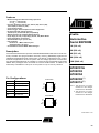
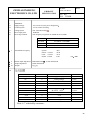
CONTENTS
Number Item
Pages
1
Safety Precaution..
3-5
2
Production Instruction Book.
6-18
3
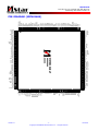
Block Diagram
19-19
4
Circuit Diagram
20-25
5
PCB layer and Component Position.
26-27
6
Explosive View
28-32
7
Basic Operations & Circuit Description
33-36
8
Simple Trouble Shoot
37-37
9
Factory Mode Setting
38-39
10
Main IC Information
40-101
11
Panel Information
102-137
12
Software Upgrade
137-140
Safety Precaution
RISK OF ELECTRIC SHOCK
DO NOT OPEN
The lightning flash with arrowhead symbol,
within an equilateral triangle, is intended to
alert the user to the presence of uninsulated
“dangerous voltage” within the product’s enclo
sure that may be of sufficient magnitude to
constitute a risk of electric shock to persons.
CAUTION: TO REDUCE THE RISK OF
ELECTRIC SHOCK, DO NOT REMOVE COVER
(OR BACK). NO USER-SERVICEABLE PARTS
INSIDE. REFER SERVICING TO QUALIFIED
SERVICE PERSONNEL ONLY.
The exclamation point within an equilateral
triangle is intended to alert the user to the
presence of important operating and
maintenance (servicing) instructions in the
literature accompanying the appliance.
CAUTION
PRECAUTIONS DURING
SERVICING
1. In addition to safety, other parts and
assemblies are specified for conformance with
MAKE YOUR CONTRIBUTION
TO PROTECT THE
ENVIRONMENT
Used batteries with the ISO symbol
such regulations as those applying to spurious
radiation. These must also be replaced only
for recycling as well as small accumulators
with specified replacements.
Examples: RF converters, tuner units, antenna
(rechargeable batteries), mini-batteries (cells) and
starter batteries should not be thrown into the
selection switches, RF cables, noise-blocking
capacitors, noise-blocking filters, etc.
garbage can.
Please leave them at an appropriate depot.
2. Use specified internal Wiring. Note especially:
1) Wires covered with PVC tubing
2) Double insulated wires
3) High voltage leads
3. Use specified insulating materials for hazardous
live parts. Note especially:
1) Insulating Tape
2) PVC tubing
3) Spacers (insulating barriers)
4) Insulating sheets for transistors
5) Plastic screws for fixing micro switches
4. When replacing AC primary side components
(transformers, power cords, noise blocking
capacitors, etc.), wrap ends of wires securely
about the terminals before soldering.
WARNING:
Before servicing this TV receiver, read the
SAFETY INSTRUCTION and PRODUCT
SAFETY NOTICE.
SAFETY INSTRUCTION
The service should not be attempted by anyone
unfamiliar with the necessary instructions on this
apparatus. The following are the necessary
instructions to be observed before servicing.
1. An isolation transformer should be connected in
the power line between the receiver and the
AC line when a service is performed on the
primary of the converter transformer of the set.
2. Comply with all caution and safety related
provided on the back of the cabinet, inside the
cabinet, on the chassis or picture tube.
5. Make sure that wires do not contact heat
generating parts (heat sinks, oxide metal film
resistors, fusible resistors, etc.)
6. Check if replaced wires do not contact sharply
edged or pointed parts.
7. Make sure that foreign objects (screws, solder
droplets, etc.) do not remain inside the set.
3. To avoid a shock hazard, always discharge the
picture tube's anode to the chassis ground
before removing the anode cap.
4. Completely discharge the high potential voltage
of the picture tube before handling. The picture
tube is a vacuum and if broken, the glass will
explode.
3
5. When replacing a MAIN PCB in the cabinet,
PRODUCT SAFETY NOTICE
always be certain that all protective are
installed properly such as control knobs,
adjustment covers or shields, barriers, isolation
resistor networks etc.
6. When servicing is required, observe the original
lead dressing. Extra precaution should be given
to assure correct lead dressing in the high
voltage area.
Many electrical and mechanical parts in this
apparatus have special safety-related
characteristics.
These characteristics are offer passed
unnoticed by visual spection and the protection
afforded by them cannot necessarily be obtained
by using replacement components rates for a
7. Keep wires away from high voltage or high
tempera ture components.
higher voltage, wattage, etc.
The replacement parts which have these
8. Before returning the set to the customer,
always perform an AC leakage current check
special safety characteristics are identified by
marks on the schematic diagram and on the parts
on the exposed metallic parts of the cabinet,
such as antennas, terminals, screwheads,metal
list.
overlay, control shafts, etc., to be sure the set
is safe to operate without danger of electrical
read the parts list in this manual carefully. The
use of substitute replacement parts which do not
shock. Plug the AC line cord directly to the
AC outlet (do not use a line isolation
have the same safety characteristics as specified
in the parts list may create shock, fire, or other
transformer during this check). Use an AC
voltmeter having 5K ohms volt sensitivity or
hazards.
9. Must be sure that the ground wire of the AC
more in the following manner.
Connect a 1.5K ohm 10 watt resistor paralleled
inlet is connected with the ground of the
apparatus properly.
Before replacing any of these components,
by a 0.15μF AC type capacitor, between a
good earth ground (water pipe, conductor etc.,)
and the exposed metallic parts, one at a time.
Measure the AC voltage across the combination
of the 1.5K ohm resistor and 0.15 uF
capacitor. Reverse the AC plug at the AC
outlet and repeat the AC voltage measurements
for each exposed metallic part.
The measured voltage must not exceed 0.3V
RMS.
This corresponds to 0.5mA AC. Any value
exceeding this limit constitutes a potential
shock hazard and must be corrected
immediately.
The resistance measurement should be done
between accessible exposed metal parts and
power cord plug prongs with the power switch
"ON". The resistance should be more than
6M ohms.
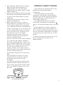
AC VOLTMETER
Good earth ground
such as the water
pipe, conductor,
etc.
Place this probe
on each exposed
metallic part
AC Leakage Current Check
4
CAUTION
Danger of explosion if battery is incorrectly replaced.
Replace only with the same or equivalent type.
%DWWHULHVVKDOOQRWEHH[SRVHGWRH[FHVVLYHKHDWVXFKDVVXQVKLQH¿UHRUWKH
like.
Used batteries should not be thrown into the garbage can, please leave them
at an appropriate depot.
CAUTION
Where the MAINS plug or an appliance coupler is used as the disconnect device,
the disconnect device shall remain readily operable.
CAUTION
7KHVHVHUYLFLQJLQVWUXFWLRQVDUHIRUXVHE\TXDOL¿HGVHUYLFHSHUVRQQHORQO\7R
reduce the risk of electric shock, do not perform any servicing other than that
FRQWDLQHGLQWKHRSHUDWLQJLQVWUXFWLRQVXQOHVV\RXDUHTXDOL¿HGWRGRVR
Attention:
Motionless picture might cause permanent destruction to the display.
• Be sure not to display motionless picture on the LCD TV for more than
2 hours, because it would cause picture remnants to appear, which is
called "screen burns". To avoid such picture remnants, please decrease
the "contrast" and "brightness" of the display when displaying motionless
picture.
• While watching TV program in 4:3 size mode for a long time, there would
be traces on the edge of the screen's left, right and center parts because
of different transmition of the light on the screen.Similar impact on the
screen will occur when playing DVD or connecting games control. Products
destroyed by these reasons can't be guaranteed for maintenance.
• It might cause picture remnants to display electronic games and motionless
picture of PC more than a period of time.To avoid such effect, please
decrease the "contrast" and "brightness" when displaying motionless
picture.
5
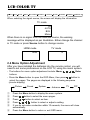
LCD COLOR TV
1. Connection and Preparation of TV
1.1 Accessories
User Manual x 1
Power Cord x 1
Remote Control x 1
%DWWHU\8053$$$[
6WDQG[3UHDVVHPEOHG2SWLRQDO
:DOO0RXQW.LW[3UHDVVHPEOHG2SWLRQDO
1.2 Installation of Stand
1. Place the TV with the front panel facing downwards on the soft cloth or soft
pads on a desk.
2. Insert the stand into the bottom socket of the TV.
3. Insert the screws into the sockets and tighten them.
1.3 Installation of Wall Mount Kit(Optional)
The Wall Mount Kit can help install the TV on the wall.
For more information about wall mounting, please refer to the instructions
provided along with the wall mount kit.
:KHQZDOOPRXQWLQJWKHSURGXFWSOHDVHFRQWDFWTXDOL¿HGSHUVRQQHO
If users choose to install the TV by themselves, the producer is irresponsible
for any possible damages caused either to the product or to persons .
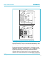
1.4 Keys and Interfaces
•
L32K6/L37K6/L42K6
1. Remote sensor window&
Power indicator
2. Speaker
3. Menu key
4. Channel “ ” key
5. Channel “ ” key
6. Volume “ ” key
7. Volume “ ” key
8. Source key
3RZHU6WDQGE\NH\
10. Power switch
11. AC input
0(',$
13. HDMI 1 input
14. HDMI 2 input
'68%9*$LQSXW
16. VGA/DVI audio input
17. YPbPr 1 and audio input
$9YLGHRDQGDXGLRLQSXW
19. S-Video input
$9YLGHRDQGDXGLRLQSXW
21. Antenna input
22. YPbPr 2 and audio input
$9YLGHRDQGDXGLRLQSXW
24.Coaxial output
$99LGHRDQGDXGLRRXWSXW
22
YPbPr 2
YPbPr 1
23
24
25
LCD COLOR TV
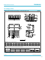
1.5 Remote Control
POW(5
SOURC(
1
2
3
4
5
6
7
8
9
DISPLAY
R(&ALL
0
)5((=( SWAP
POS
PIP
VOL
+
CH
MU7(
_
^
^
0(18
P.6,=(
ENTER
602'(
>
7(;7
V-CHIP
CCD
&(
P.02'( ,1'(;
PA*(
HOLD
5(9($/ 6,=(
MI;
LIST
5(D
*5((1 <(//2W
BLU(
32:(56WDQGE\WXUQRQDQGRII
6285&(6HOHFWWKHVLJQDOVRXUFH
3. 0~9: Continue to press the keys to select
a channel.
4. DISPLAY: Display the information of
current video and audio.
5(&$//5HWXUQWRSUHYLRXVFKDQQHO
)5((=()UHH]HWKHSLFWXUH
7. PIP: Open or close PIP.
8. SWAP: Swap the position of the main
picture and sub picture.
9. POS: Change the PIP position.
10. VOL+: Increase the volume.
11. CH∧: Select the channel forward.
087(0XWHVRXQG
13. VOL-: Decrease the volume.
14. CH∨: Select the channel backward.
0(18(QWHURUH[LWPHQX
36,=(&KDQJHWKHSLFWXUHVL]H
17. , , , key: The menu item selection.
18. (17(5&RQ¿UPRUHQWHU
602'(6HOHFWWKHVRXQGPRGH
7(;7RSWLRDO(QWHURUH[LWWHOHWH[W
&(+LGHWHOHWH[WFRQWHQWVSUHVVDJDLQWR
reappear.
302'(6HOHFWWKHSLFWXUHPRGH
23. HOLD: Hold the current page.
,1'(;'LVSOD\WKHLQGH[SDJH
3$*((QWHUWKHVXESDJHPRGH
5(9($/5HYHDOWKHKLGGHQLQIRUPDWLRQ
/,67(QWHUWKHWHOHWH[WOLVWPRGH
6,=(&KDQJHWKHWHOHWH[WVL]H
0,;3UHVVUHSHDWHGO\WRWXUQRQ7HOHWH[W
Teletext blending with TV program
Teletext mode.
5('$FFHVVWKHUHGLWHPRUSDJH
%/8($FFHVVWKHEOXHLWHPRUSDJH
*5((1$FFHVVWKHJUHHQLWHPRUSDJH
<(//2:$FFHVVWKH\HOORZLWHPRU
page.
Note: The INDEX, CE, PAGE, HOLD,
REVEAL, SIZE, MIX, LIST, RED,
GREEN, YELLOW, BLUE keys related
to teletext are optional.
1.6 Installation of Batteries
1. Open the back lid of the remote control.
,QVWDOOWZR$$$9EDWWHULHV
(QVXUHWKHFRUUHFWSRODULW\RIWKHEDWWHULHV
3. Cover the back lid.
Please take out of the batteries from the remote
control for long time of no use.
If the remote control doesn't work properly,
please carry out the following checks.
- Check the TV is turned on.
- Check the polarity of the batteries are correct.
- Check the batteries are not drained.
- Check the power supply is normal or the power cord
is correctly connected.
&KHFNWKHUHDUHQRVSHFLDOÀXRUHVFHQWOLJKWRUQHRQ
light around.
2. Basic Operation
2.1 Power ON/OFF
- Connect the power cord to the AC Input. Insert the power cord into the
appropriate socket.
- Press the Power switch to switch on the TV, then press Power button to
turn on the unit.
- Press the Power switch again to switch off the TV.
Note: After switch off the TV, please don’t immediately re-open the power
switch ,should be delayed one minute more to re-open the power
switch.
2.2 Setting of Standby Mode
- Press Power ( EXWWRQWRWXUQRQWKHXQLW
- Press Power ( EXWWRQDJDLQWRUHWXUQWKHGLVSOD\WRVWDQGE\PRGH7KH
power indicator turns red.
- Be sure not to set your TV in standby mode for a long period of time.
2.3 Selection of Input Mode
- Press the Source button, and then press or
to select the signal
source you desire, then press Enter or EXWWRQWRFRQ¿UP 7KHVLJQDOVRXUFHVDUHGLVSOD\HGLQWKHIROORZLQJVHTXHQFH
LCD COLOR TV
TV
AV1
AV2
AV3
69,'(2
YPbPr1
YPbPr2
VGA
HDMI1
HDMI2
0(',$
When selecting the signal source, the screen will display the information.
TV mode
59
AUTO
B/G
Mono
When there is no signal from the selected source, the warning
message will be displayed DVSHULOOXVWUDWLRQ(LWKHUFKDQJHWKHFKDQQHO
in TV mode or press Source button to change source.
HDMI mode
TV mode
HDMI
12
2.4 Menu Option Adjustment
After you have installed the batteries into the remote control, you will
need to set some preferences on the LCD TV, using the menu system.
- The buttons for menu option adjustment include: Menu, , , ,
Enter
buttons.
- Press the Menu button to open the OSD Menu, then press , button to
VHOHFWWKHSDJHV7KHSDJHVDUHGLVSOD\HGLQWKHIROORZLQJVHTXHQFH
FLUFXODUGLVSOD\
Picture
Sound
System
Advance
TV
PIP
Press the Menu button to display the menu system.
Press , button to select the menu pages.
Press
,
button to select an item.
Press , , ,
button to select or adjust a setting.
If you do not make a selection within 15 seconds, the menu will close
automatically.
Press the Menu button to return or exit OSD menu.
2.5 Menu Functions
2.5.1 Picture Function
Ć Adjustment of the Picture.
Press the Menu button, and then press
or button until the “Picture” menu
appears.
Press
or
button to highlight the
“Picture Mode”,“Contrast”,“Brightness”,
“Hue”,“Saturation” “Sharpness”,“Color
Temp”,“Picture Size”item.
Press or button to adjust.
Press the Menu button to return or exit.
Pictuer Mode
Contrast
Brightness
Standard
60
50
Saturation
Sharpness
Select
50
50
Adjust
Exit
2.5.2 Sound Function
Ć Adjustment of the Sound
Press the Menu button, and then press
or button until the “Sound” menu
appears.
or
button to highlight the
Press
“Sound Mode”, “Bass”, “Treble”,
“Balance”,“Sourround”, “NICAM” item.
Press or button to adjust.
Press the Menu button to return or exit.
Note: “NICAM” item is optional.
Sound Mode
Standard
Surround
Select
Off
Adjust
Exit
2.5.3 System Function
Ć Adjustment of the System
Press the Menu button, and then press
or button until the “System” menu
appears.
or
button to highlight the
Press
“OSD Language”,“OSD Halftone”,
“Default” item.
button to adjust.
Press or
Press the Menu button to return or exit.
OSD Language
Select
(QJOLVK
Adjust
Exit
LCD COLOR TV
2.5.4 Advance Function
Ć Adjustment of the Advance
To control the noise reduction.
Press the Menu button, and then press
or button until the “Advance” menu
appears.
Press
or
button to highlight the
³'15´³6OHHS´³77;/DQJXDJH´LWHP
Press or button to select .
Press the Menu button to return or exit.
Note: ,QDFWLYHIRU9*$DQG'9,ĺ+'0,
0,''/(
3D NR
77;/DQJXDJH
Select
:(67
Exit
Adjust
2.5.5 TV Function (Optional) (Only for TV)
Ć Adjustment of the TV
Press the Menu button, and then press
or
button until the “TV” menu
appears.
Press
or
button to highlight the
“Channel”, “Color System”, “Sound
System”, “Skip”, , “FineTuning”,
“Manual Search”, “Auto Search” item.
Press or
button to select .
Press the Menu button to return or exit.
T V
Channel
Color System
Sound System
Select
0
PAL
DK
Exit
Adjust
2.5.6 PIP Function
Ć Adjustment of the PIP
Press the Menu button, and then press
or
button until the “PIP” menu
appears.
Press
or
button to highlight the
“Multi Window”,“Sub Source”,“Size”,
“PIP H-Position”,“PIP V-Position”,
“Border Color”,“Sound Source”,
“Swap” item.
Press or
button to adjust.
Press the Menu button to return or exit.
Large
Size
PIP H-Position
PIP V-Position
Border Color
Select
1
Black
Adjust
Exit
PIP Setting23,3IXQFWLRQ;QRQ3,3IXQFWLRQ
Sub
Main
TV
AV
S-Video
YPbPr
TV
AV
S-Video
YPbPr
VGA
HDMI
;
;
;
O
;
;
;
O
;
;
;
O
O
O
O
;
O
O
O
;
O
O
O
;
VGA
HDMI
O
O
O
O
O
O
;
;
;
;
;
;
2.5.7 Geometry Function (Only for VGA )
Ć Adjustment of the Geometry
Press the Menu button, and then press
or
button until the “Geometry”
menu appears.
or
button to highlight the
Press
“H-Position”,“V-Position”,“Clock”,
“Phase”, “Auto” item.
Press or
button to adjust.
Press the Menu button to return or exit.
Geometry
Clock
Phase
Auto
Select
Adjust
Exit
2.5.8 MEDIA Function (Option )
Ć $GMXVWPHQWRIWKH0(',$
In0(',$6RXUFHWKH0(',$0(18ZLOO
always appear as right.
Press
or
button to select
-3(*03RU'(9,&(IXQFWLRQ7KH
-3(*RQO\VXSSRUWMSJIRUPDWGDWD03
only support.mp3 format data the device
only support FAT32 format hard disk.
button to highlight the
Press or
-3(*RU03¿OHWKHSUHVVEXWWRQWR
play music or decording picture.
Press the Menu button to return or exit.
-3(*
LCD COLOR TV
2.6 Using the Teletext Function (Optional)
Note: When pressing the Teletext function keys on the remote control, if the
word “NO TTX” is displayed onscreen, it means the related function
can’t be used.
Teletext is a free service broadcast by most TV stations which give up-to-theminute information news,weather,television programs, share price,subtitles,and
many other topics.
7RRSHUDWH7(/(7(;7
Ć Select a TV station on which Teletext is being transmitted.
Ć Press the Text button once to bring up the teletext screen.Two page
QXPEHUVDUHGLVSOD\HGRQWKHVFUHHQKHDGOLQH7KH¿UVWSDJHQXPEHU
indicates your selection,while the second shows the current page
displayed.
Teletext Page Selection
Ć (QWHUWKHUHTXLUHG7HOHWH[WSDJHDVDWKUHHGLJLWQXPEHUV7KHVHOHFWHG
page number is displayed at the top left corner of the screen. The
Teletext page counter searches until the selected page number is
located,so that the desired page is displayed on the screen.
Ć The , buttons can be used to select the preceding or following page.
Ć )DVW¿QGXVLQJWKH4 coloured buttons.Four subject-headed pages
FDQEHVHOHFWHGTXLFNO\E\SUHVVLQJWKHFRUUHVSRQGLQJFRORXUHGEXWWRQV
Red,Green,Yellow,or Blue on the remote control.
Useful features for Teletext
Mix
Ć Press repeatedly to turn on Teletext Teletext blending with TV program
Teletext mode.
Index
Ć Press this button to select the index page that displays the list of teletext
contents.
Hold
Ć The teletext page you have selected may contain more information than
is on the screen;The rest of the information will be displayed after a
period of time on a sub page.
Ć Press Hold button to stop the automatic page change.The hold symbol
will be displayed at the top left-hand corner on the screen and the
automatic page change will be stopped.
Ć Press Hold button again to continue.
Reveal
Ć Press this button once to display concealed information,such as solutions
RIULGGOHVSX]]OHVRUDTXL]
Ć Press this button again to conceal the revealed answers.
Size
Ć Press repeatedly to double the character size in the following order:Upper
half of the page, Lower half of the page, Return to normal size.
Page
Ć Press this button to enter the sub page mode.You can use , button
to display sub page; Press again to exit.
CE
Ć Press to hide teletext contents, press again to reappear.
List
Ć Press this button to list mode, press again to exit.
LCD COLOR TV
7HFKQLFDO6SHFL¿FDWLRQ
Product Model
Screen Size
L32K6
L37K6
L42K6
32” diagonal
37” diagonal
42” diagonal
Aspect Ratio
16:9
Power Supply
AC 100-240V~ , 50/60 Hz
Power
Consumption
TV System
140 W
Audio Output
Power
,QWHUQDO
6W x 2
Input Terminal
Output
Terminal
200 W
280 W
3$/%*'.,6(&$0%*'.
6W x 2
8W x 2
$QWHQQD,QSXW',17\SH[
9*$'6XE3LQ7\SH[
+'0,9HU&RQQHFWRU[
S-Video Input Mini Din 4 Pin Terminals x 1
Video Input RCA Terminals x 3
Component Video - YPbPr x 2 RCA Terminals
Stereo Audio x 3RCA,x 1( Phone Jack for VGA/DVI)
0(',$86%7\SH[
VHWRI$XGLR2XWSXW7HUPLQDOV5&$/5
1 set of Video Output RCA Terminals
1 set of S/PDIF Output RCA Terminals
Outline Size
/[:[+PP
without stand
with stand
799x88x529
799x236x564
914x93x595
914x236x634
1022x93x657
1022x256x712
Gross Weight
15.2Kg
19.2kg
22.5kg
Working
Temperature
Working
Humidity
0ć~40ć
20% ~ 80% Non-condensing
4. Supported Signal Modes
A. VGA Mode
Resolution
640 x 480
800 x 600
1024 x 768
Horizontal
)UHTXHQF\
.+]
31.50
35.16
37.90
48.40
Vertical
)UHTXHQF\
+]
60.00
56.25
60.00
60.00
Note: 1. When in VGA mode, you’d better choose the resolution of 1024 x 768.
2. You’re suggested to use the VGA connecting cord of not more than 5
meters to ensure the appropriate picture quality.
B.
YPbPr Mode
Resolution
480i
S[
576i
S[
S[
1080i
3[
C.
Horizontal
)UHTXHQF\
.+]
15.734
31.468
15.625
31.25
37.50
45.00
28.13
33.75
67.50
56.25
Vertical
)UHTXHQF\
+]
59.94
59.94
50.00
50.00
50.00
60.00
50.00
60.00
60.00
50.00
HDMI Mode
Resolution
480p
576p
720P
1080i
3[
Horizontal
)UHTXHQF\
.+]
31.468
31.25
45.00
33.75
67.50
Vertical
)UHTXHQF\
+]
59.94
50.00
60.00
60.00
60.00
Note: HDMI mode can't be applied to PC function.
- When the signal received by the Display exceeds the allowed range, a
warning message will appear on the screen.
<RXFDQFRQ¿UPWKHLQSXWVLJQDOIRUPDWRQVFUHHQ
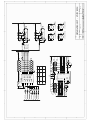
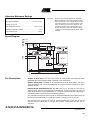
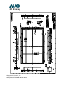
Simplified Functional Block Diagram
Mstar-6E16GS Chassis
W
TV IF
DC-DC POWER
UZ1084 3.3V
UZ1084 1.26V/2.5V
TUNER
ET-5C511-BS1A
SAWFILER
FLASH RAM
W25VF032
EEPROM
AT24C64
PANEL VDD
PANELPower
Switch
AP2309
SIF/PIF
AV VIDEO
CONTROL SIGNAL
S-Video
PANEL
SCALER
Mstar6E16GS
AV1 Audio
LVDS SIGNAL
VGA
HDMI 1/2
COMP-V 1
COMP-V 2
YPbPr SWITCH
PI5V330Q
AV2 Audio
AV AUDIO SWITCH
COMP-V1
UTC4052
Audio OUT
DDR RAM
128M-4ns
AUDIO
BUFFER
AUDIO AMPLIFIER
TDA8944J
DC 12V For AUDIO
SMPS(PSU)PCB Ass'y
AC POWER IN
HDZ1804-3A
AMP
DC 5V For System VSS
DC 12V For System VSS
DC 24V For Inverter VSS
L
R
D
P_3.3V_VIF
GND
VI_TV_VIF+
VI_TV_VIF-
AU_TV_SIF-
AU_TV_SIF+
GND
P_3.3V_SIF
1
IIC_ SCL_H2
SW_TV_AGC
RE F_ VR2 7
IIC_ SDA_H2
P_3.3V_ AU
P_3.3V_MPLL
SW_H2_HPD
GND
X_IN
VI_H2_T X2-
REF_AU_P
X_OUT
VI_H2_T X2+
GND
GND
GND
REF_AU
VI_CVBS1_Out
VI_H2_T X1+
P_3.3V_ AU
VI_CVBS2_Out
VI_H2_T X1-
AU_VGA_ L
P_3.3V_AVDD
GND
AU_VGA_ R
VI_AV1_Vin-
VI_H2_T X0+
AU_MUX_ L
VI_AV1_Vin+
VI_H2_T X0-
AU_MUX_ R
C
P_3.3V_ AVDD
AU_GND
VI_AV2_Vin-
VI_H2_CLK+
MST6E16GS-LF
MST6E16G-LF
MST6E16G-LF
AU_Out_L3
VI_AV2_Vin+
VI_H2_CLK-
AU_Out_R3
VI_AV3_Vin
P_1.2V_ C
AU_Out_L2
VI_S1 _Cin
SW_PDP_DISPEN
AU_Out_R2
VI_S1 _Yin
SW_USB_DET
AU_Out_L1
SW _SC2_FB
GND
AU_Out_R1
VI_VGA_VS
P_3.3V_ VDDP
SW_YPbPr
VI_VGA_HS
VI_LV_RA0SW_TV_SIF
GND
VI_LV_RA0+
SW_MUTE_M
P_3.3V_AVDD
VI_LV_RB0P_3.3V_ VDDP
VI_VGA_RIN+
VI_LV_RB0+
GND
VI_VGA_SOG
VI_LV_RC0P_1.2V_ C
VI_VGA_GIN+
VI_LV_RC0+
SW_SC1_FS
VI_VGA_GIN-
VI_LV_CK0SW_P_STB
VI_VGA_BIN+
VI_LV_CK0+
SW_SC2_FS
VI_VGA_BIN-
2
SW_SC1_FB
VI_SW _RIN+
VI_LV_RD0+
AU_SPDIF_O
VI_SW _GIN+
VI_LV_RE0SW_4052 _1
VI_SW _SOG
VI_LV_RE0+
SW_4052 _2
B
GND
DDR_BA1
VI_SW _BIN+
P_3.3V_ VDDP
DDR_BA0
RE F_ ADC_N
VI_LV_RA1DDR_RASZ
RE F_ ADC_P
VI_LV_RA1+
P_1.2V_ C
RE F_ SCALER
VI_LV_RB1GND
IIC_SCL_ H1
VI_LV_RB1+
P_2.5V_ MEM
IIC_SDA_H1
VI_LV_RC1DDR_CASZ
REF_HDMI
VI_LV_RC1+
DDR_WEZ
SW _H1_HPD
VI_LV_CK1DDR_AR11
VI_H1_TX2+
VI_LV_CK1+
DDR_AR10
VI_H1_TX2-
VI_LV_RD1DDR_AR9
VI_H1_TX1+
VI_LV_RD1+
DDR_AR8
VI_H1_TX1-
VI_LV_RE1DDR_AR7
P_3.3V_AVDD
VI_LV_RE1+
DDR_AR6
VI_H1_TX0+
P_1.2V_ C
DDR_AR5
VI_H1_TX0-
GND
DDR_AR4
RXACKN
RXACKP
RXA0N
RXA0P
AVDD_33
RXA1N
RXA1P
RXA2N
RXA2P
HOTPLUGA
REXT
DDCDA_SDA
DDCDA_SCA
VCLAMP
REFP
REFM
BIN1P
SOGIN1
GIN1P
RIN1P
BIN0M
BIN0P
GIN0M
GIN0P
SOGIN0
RIN0P
AVDD_33
GND
HSYNC0
VSYNC0
VSYNC2
Y0
CVBS3
CVBS2
CVBS1
VCOM1
CVBS0
VCOM0
AVDD_33
CVBSOUT1
CVBSOUT0
GND
XOUT
XIN
AVDD_MPLL
GND_VIFPLL
VR27
AVDD_RXS
GND_RXS
SIFP
SIFM
VIFM
VIFP
AVDD_RXV
SW_RESE T
DDR_AR3
1
2
3
4
5
6
7
8
9
10
11
12
13
14
15
16
17
18
19
20
21
22
23
24
25
26
27
28
29
30
31
32
33
34
35
36
37
38
39
40
41
42
43
44
45
46
47
48
49
50
51
52
53
54
SW_5V_USB
DDR_AR2
VI_H1_CLK+
P_3.3V_ VDDP
DDR_AR1
VI_H1_CLK-
SW_LCD_ BLK
DDR_AR0
A
VI_LV_RD0-
2
SW_LCD_ ADJ
GND
1
VI_TV_IR
P_3.3V_ AVDD
216
215
214
213
212
211
210
209
208
207
206
205
204
203
202
201
200
199
198
197
196
195
194
193
192
191
190
189
188
187
186
185
184
183
182
181
180
179
178
177
176
175
174
173
172
171
170
169
168
167
166
165
164
163
DDCDB_SCL
DDCDB_SDA
HPLUGB
RXB2P
RXB2N
GND
RXB1P
RXB1N
GND
RXB0P
RXB0N
AVDD_33
RXBCKP
RXBCKN
VDDC
GPIOM[1]
GPIOM[0]
GND
VDDP
LVB0M
LVB0P
LVB1M
LVB1P
LVB2M
LVB2P
LVBCKM
LVBCKP
LVB3M
LVB3P
LVB4M
LVB4P
GND
VDDP
LVA0M
LVA0P
LVA1M
LVA1P
LVA2M
LVA2P
LVACKM
LVACKP
LVA3M
LVA3P
LVA4M
LVA4P
VDDC
GND
HWRESET
GPIOT[1]
VDDP
PWM3
PWM2
VDDP
IRIN
P_2.5V_ MEM
55
56
57
58
59
60
61
62
63
64
65
66
67
68
69
70
71
72
73
74
75
76
77
78
79
80
81
82
83
84
85
86
87
88
89
90
91
92
93
94
95
96
97
98
99
100
101
102
103
104
105
106
107
TAGC
AVDD_33
GND
AUVRM
AUVRP
AUVAG
AVDD_AU
LINE_IN_0L
LINE_IN_0R
LINE_IN_1L
LINE_IN_0R
AUCOM
LINE_OUR_3L
LINE_OUT_3R
LINE_OUT_2L
LINE_OUT_2R
LINE_OUT_1L
LINE_OUT_1R
GPIOD[0]
GPIOD[1]
GPIOD[2]
VDDP
GND
VDDC
AD[0]
AD[1]
AD[2]
AD[3]
WRZ
RDZ
ALE
BADR[1]
BADR[0]
RASZ
VDDC
GND
AVDD_MI
CASZ
WEZ
MADR[11]
MADR[10]
MADR[9]
MADR[8]
MADR[7]
MADR[6]
MADR[5]
MADR[4]
MADR[3]
MADR[2]
MADR[1]
MADR[0]
GND
AVDD_MI
AVDD_MIPLL
P_3.3V_ MIPLL 108
3
INT
DDCA_SCL
DDCA_SDA
DDCR_SCL
DDCR_SDA
PWM1
PWM0
SAR3
SAR2
SAR1
SAR0
VDDC
GND
SPI_SDO
SPI_SCZ
SPI_SDI
SPI_SCK
VDDP
GND
USB20_DP
USB20_DM
AVDD_USB
USB20_REXT
MVREF
MCLKE
MCLK
MCLKZ
DQM1
DQS1
AVDD_MI
MDATA[15]
MDATA[14]
MDATA[13]
MDATA[12]
AVDD_MI
MDATA[11]
MDATA[10]
GND
MDATA[9]
MDATA[8]
AVDD_MI
MDATA[7]
MDATA[6]
MDATA[5]
MDATA[4]
AVDD_MI
MDATA[3]
MDATA[2]
GND
MDATA[1]
MDATA[0]
AVDD_MI
DQS0
DQM0
U103
3
162
161
160
159
158
157
156
155
154
153
152
151
150
149
148
147
146
145
144
143
142
141
140
139
138
137
136
135
134
133
132
131
130
129
128
127
126
125
124
123
122
121
120
119
118
117
116
115
114
113
112
111
110
109
P_3.3V_AVDD
C123
C109
100n
C110
4.7uF
C112
100n
SPI_DI
C117
100n
RE F_ DDR
Date:
File:
A4
Size
Title
DDR_ LDQM
DDR_ DQS0
P_2.5V_MEM
DDR_ DATA0
DDR_ DATA1
R140
R139
4.7K
SW _YPbPr
4.7K
SW _TV_SIF
P_3.3V_M
R135
4.7K
P_5Vs_SA
100K
47K
R132
R131
4.7K x 4
R138
4.7K x 4
R149
SW _USB_DE T
SW _4052_2
SW _4052_1
SW _P_STB
SW _MUTE_M
SW _5V_PANEL
VI_TV_IR
SW _LCD_ADJ
SW _LCD_BLK
SW _5V_USB
GND
P_5V_USB
PAGE 1 / 8
4
2009-5-22
Sheet of
Drawn By:
E:\䆒䅵ᮍḜ\MST6M16_FILE\Scaler.SCHDOC
Number
Revision
MST6E16
FANGDW
REV1.0
MST6E16PROJECT - SCALER
P_3.3V_M
4.7K x 4
SW _TV_KEY
P_3.3V_M
DDR_ DATA2
GND
SW _TV_KEY1
DDR_ DATA3
SW _WP_FSH
SW _LED
SW _WP_M
SW _TV_KEY2
R150
4.7K x 4
P_2.5V_MEM
DDR_ DATA4
DDR_ DATA5
DDR_ DATA6
R133 4.7K
R134 4.7K
IIC_SDA_M
DDR_ DATA8
IIC_SCL_ VGA
REF_HDMI
IIC_SCL_ M
DDR_ DATA7
RE F_ VR2 7
RE F_ AU
RE F_ AU_ P
RE F_ ADC_N
C108
100n/nc
RE F_ ADC_P
RE F_ USB
DDR_ DATA9
P_2.5V_MEM
RE F_ DDR
R101
10K
RE F_ SCALER
IIC_SDA_VGA
R148
390
R104
GND
10K
GND
DDR_ DATA10
DDR_ DATA11
P_2.5V_MEM
DDR_ DATA12
DDR_ DATA13
DDR_ DATA14
DDR_ DATA15
P_2.5V_MEM
DDR_ DQS1
DDR_ UDQM
DDR_ MCLK-
DDR_ MCLK+
DDR_ CKE
RE F_ USB
P_3.3V_A
C116
10uF
P_3.3V_VDDP
VI_USB_D-
100n
C115
4.7uF
R103
910
C114
1uF
VI_USB_D+
GND
P_3.3V_VDDP
SPI_CK
SPI_CZ
GND
SPI_DO
C107
100n
P_1.2V_C
SW _TV_KEY
SW _TV_KEY1
SW _TV_KEY2
SW _WP_FSH
SW _LED
SW _WP_M
IIC_SDA_M
C106
100n
C105
100n
IIC_SCL_ M
IIC_SDA_VGA
C104
1n
IIC_SCL_ VGA
SW _5V_PANEL
R102
P_2.5V_MEM
4
D
C
B
A
D
C
B
A
CN102
4
C120
R154
1M
R120 100
Y101
27p 14.318M
100
100
R115
R114
SDA
SCL
WP
VCC
5
6
7
8
100n
GND
P_5Vs_SA
100
100
R118
220
R155
X_OUT
X_IN
0
33X 4
SPI_DO
SPI_CZ
SPI_DI
SPI_CK
P_5Vs_SA
GND
C121
1uF
1K
R153
Q101
N3906
100
R116
CN5/PH2.0
1K
R152
10K
R121
C122
1nF
2
SW _RESET
GND
C118
100uF
P_3.3V_A
IIC_SDA_M
IIC_SCL_ M
SW _WP_M
P_5Vs_SA
2
CN101
P_3.3V_A
SW _WP_FSH
FB/0603
L101
R111
D101
BAV99
R151
10K
R142
4.7K
R117
EEPROM FOR MAIN CPU
24C32_SOP8
GND
E2
E1
NC
U104
C103
IIC_SDA_VGA
27p
5
6
7
GND
C101
100n
GND
R141
4.7K R110
IIC_SDA_M
4.7K/NCGND
IIC_SCL_ M
R113
EEPROM FOR HDCP KEY
24C04_SO8
SDA
SCL
WP
VCC
8
100n
C102
R119 100
IIC_SDA_VGA'
C119
1
4.7K
GND
E2
E1
NC
U105
R122
5
6
7
8
R112
100
SI
SCK
HOLD
VCC
FLASH
GND
WP
SU
CE
U101
PMC25L080
IIC_SCL_ VGA
GND
4
3
2
1
4
3
2
1
R109
100n
4
3
2
1
IIC_SCL_ VGA'
GND
GND
GND
CN4/PH2.0
1
1
2
5
1
1
DDR_ AR3
DDR_ AR2
DDR_ AR1
DDR_ AR0
DDR_ BA1
DDR_ BA0
DDR_ RASZ
DDR_ CASZ
DDR_ WEZ
DDR_ LDQM
DDR_ DQS0
DDR_ DATA7
DDR_ DATA6
DDR_ DATA5
DDR_ DATA4
DDR_ DATA3
DDR_ DATA2
DDR_ DATA1
DDR_ DATA0
P_2.5V_DMC
P_2.5V_DMQ
22X4
R146
22X4
R144
R127 100
R125 100
100X4
R107
100X4
R105
3
GND
3
1
2
3
4
5
6
7
8
9
10
11
12
13
14
15
16
17
18
19
20
21
22
23
24
25
26
27
28
29
30
31
32
33
Date:
File:
A4
Size
Title
HY 5DU281622ET-4
MVDD
DQ0
VDDQ
DQ1
DQ2
VSSQ
DQ3
DQ4
VDDQ
DQ5
DQ6
VSSQ
DQ7
NC
VDDQ
LDQS
NC
MVDD
NC
LDM
WE
CAS
RAS
CS
NC
BA0
BA1
A10/AP
A0
A1
A2
A3
MVDD
U102
66
65
64
63
62
61
60
59
58
57
56
55
54
53
52
51
50
49
48
47
46
45
44
43
42
41
40
39
38
37
36
35
34
GND
150
R147
R130
22X4
R145
100X4
R123 100
R124 10K
C111 1nF
C113 0.1uF
R128 100
R108
100X4
R106
22X4
R143
10K
33X4
DDR_ AR4
DDR_ AR5
DDR_ AR6
DDR_ AR7
DDR_ AR8
DDR_ AR9
DDR_ AR10
DDR_ AR11
DDR_ CKE
DDR_ MCLK+
DDR_ MCLK-
DDR_ UDQM
GND
R126
DDR_ DQS1
DDR_ DATA8
DDR_ DATA9
DDR_ DATA10
DDR_ DATA11
DDR_ DATA12
DDR_ DATA13
DDR_ DATA14
DDR_ DATA15
PAGE 2 / 8
4
2009-5-22
Sheet of
E:\䆒䅵ᮍḜ\..\DDR&EPROM.SCHDOC Drawn By:
Number
REV1.0
MST6E16
FANGDW
Revision
MST6E16PROJECT - DDR
VSS
DQ15
VSSQ
DQ14
DQ13
VDDQ
DQ12
DQ11
VSSQ
DQ10
DQ9
VDDQ
DQ8
NC
VSSQ
UDQS
NC
VREF
VSS
UDM
CLK
CLK
CKE
NC
NC
A11
A9
A8
A7
A6
A5
A4
VSS
4
D
C
B
A
D
C
B
A
SCART2
J402
SCART1
J401
1
AOR
AIR
AOL
Gnd
Gnd
AIL
B
SWITCH
Gnd
CLK
G
DATA
Gnd
Gnd
R/C
BLANK
Vo_G
Vi_Gnd
Vout
VIN
SHIELD
AOR
AIR
AOL
Gnd
Gnd
AIL
B
SWITCH
Gnd
CLK
G
DATA
Gnd
Gnd
R/C
BLANK
Vo_G
Vi_Gnd
Vout
VIN
SHIELD
1
1
2
3
4
5
6
7
8
9
10
11
12
13
14
15
16
17
18
19
20
21
1
2
3
4
5
6
7
8
9
10
11
12
13
14
15
16
17
18
19
20
21
AU_SC1_R'o ut
GND
GND
SWITCH
BLUE
GND
D420 C414 R431
10pF 100p 75
BLUE
10K
R404
GND
10K
R406
75
R422
R424
75
RED/C
FB/0603
L405
RED/C
R413 C404
10K 560p
D432 R457 C423
10p
75
1nF
GREEN
FB/0603
L404
GREEN
FB/0603
FB/0603
L402
L401
GND
SWITCH
VI_SC1_CVBS'
AU_SC1_L'
AU_SC1_L'out
AU_SC1_R'
2
BLANK
R448 4.7K
C420 R445 C421
1nF 100K 1nF
R436
1K
R440
100K
BLANK
R416 4.7K
R433
1K
C319
1nF
C328
1nF
GND
R366
C304
C310
C324
100
L406
C302
2.2uF
C307
2.2uF
GND
C410
47nF
FB/0603
AU_Y1_L'
AU_Out_ L3
AU_Y1_R'
AU_Out_ R3
VI_AV1_Vin-
VI_AV1_Vin+
VI_SC1_Out
SW _SC1_FB
VI_S1 _Cin'
SW _SC1_FS
VI_AV2_Vin-
VI_Y2_Pr'
VI_SC2_Out
SW _SC2_FB
VI_Y1_Pr'
VI_Y1_Y'
VI_Y1_Pb'
SW _SC2_FS
C417 R441
100p 15K
FB/0603
47nF
AU_AV1_L
AU_Out_ L2
AU_AV1_R
AU_Out_ R2
C403 R410
100p 15K
D418 R429 C413
10p
75
1nF
C409
47nF
L403
C316
2.2uF
R405
1K
R409
100K
C325
2.2uF
R403
1K
R414 C405 C406 R415 C407
10K 560p 1nF 100K 1nF
C402
2.2uF
C401
2.2uF
2
3
GND
23
22
21
20
GND
23
22
21
20
3
HD MI
19
1
J404
HD MI
19
1
J403
D419
10pF
D415
10pF
D413
0.15p
D411
0.15p
D409
0.15p
D407
0.15p
TX2+
GN D
TX2TX1+
GN D
TX1TX0+
GN D
TX0CLK+
GN D
CLKCEC
NC
DDC SCL
GN D
DDC SDA
+5V HDMI
HPD
Date:
File:
A4
Size
Title
GND
GND
R435
D430
10pF
1K
R459
GND
BAT54C
D403
HDMI EDID
SW _H2_HPD
P_5V_SC
SW _H1_HPD
P_5V_SC
100 IIC_SDA_H1
100 IIC_SCL_ H1
R454 R455
4.7K 4.7K
10
10 VI_H1_CLKR451
R452
VI_H1_CLK+
10
10 VI_H1_TX0-
VI_H1_TX0+
10
10 VI_H1_TX1-
VI_H1_TX1+
10 VI_H1_TX2-
Q402
N3904
R456
4.7K
D428 R449
0.15p R450
D426 R446
0.15p R447
D424 R439
0.15p R442
BAT54C
D401
10 VI_H1_TX2+
GND
1K
R432
HDMI EDID
100 IIC_SDA_H2
100 IIC_SCL_ H2
R426 R427
4.7K 4.7K
10
10 VI_H2_CLKR423
R425
VI_H2_CLK+
10
10 VI_H2_TX0-
VI_H2_TX0+
10
10 VI_H2_TX1-
VI_H2_TX1+
10 VI_H2_TX2-
10 VI_H2_TX2+
Q401
N3904
4.7K
R430
D422
0.15p R438
D416
10pF
D414 R420
0.15p R421
D412 R417
0.15p R418
D410 R411
0.15p R412
D408
0.15p R408
R407
PAGE 3 / 8
2009-5-22
E:\䆒䅵ᮍḜ\..\Terminal input.SCHDOC
Number
4
Sheet of
Drawn By:
REV1.0
MST6E16
FANGDW
Revision
MST6E16PROJECT - TERMINAL1
D431
10pF
D429
10pF
D427
0.15p
D425
0.15p
D423
0.15p
D421
0.15p
HDMI INPUT
TX2+
GN D
TX2TX1+
GN D
TX1TX0+
GN D
TX0CLK+
GN D
CLKCEC
NC
DDC SCL
GN D
DDC SDA
+5V HDMI
HPD
HDMI INPUT
4
D
C
B
A
J301
CN301
Y
C
SPDIF
D301
10p
1
S_VIDEO&SPDIF
2
4
6
7
8
9
He adphone
75
5p
75
5p
R480
C445
R484
C451
10K
R372
VI_S1 _Cin'
10K
R368
R
L
R377
47
FB/0603
C333
47nF
C329
2.2uF
C327
2.2uF
R458
47
47nF
R357 75 L301
GND
R373 C330 R374 C331
10K 560p 10K 560p
GND
D302 R365 C323
10p 75
100p
R362
C321
47
R492 C459 R493 C460
10K 560p 10K 560p
L
R
GND
R401
R402
47
47
390
47
VI_S1 _Yin
VI_S1 _Cin
AU_SPDIF_O
AU_AV3_L
AU_AV3_R
VI_Y2_Pr'
C454
2.2uF
C441
C442
C444
C446
C448
2
C453
2.2uF
47nF
1nF
47nF
47nF
47nF
AU_VGA_R
AU_VGA_L
VI_VGA_RIN+
VI_VGA_GIN-
VI_VGA_GIN+
VI_VGA_SOG
VI_VGA_BIN-
VI_VGA_BIN+
VI_VGA_HS
IIC_SCL_ VGA'
IIC_SDA_VGA'
VI_VGA_VS
100
100
P_5V_SC
100
47
C436 47nF
R465
4.7K
2
100
VI_AV3_Vin
L410 FB/0603 R483
C449 5p
C443
L408
C437
L407
BAT54C
D405
D437 C430 R466
10p100p/NC 4.7K
100n
C427
R472
R473
FB/0603 R474
5p
R478
FB/0603 R479
5p
R481
D436 C429
10p 1nF/NC
R464
1K
R378
C335
C320
47nF
C336 47
C337
100p/NC
1nF/NC
100p/NC
D304 R382
D303 R381
R361 10p 75
10p 75
100
100n
C318
GND
75
5p
R475
C440
D434 D435
10p 10p
R463
1K
D441 D442 D443
0.15p 0.15p 0.15p
R487
10K
R488
10K
GND
VGA AUDIO INPUT
J410
4/L
2/R
SCL
5 GN D
GN D
VSYNC
MRXD
+5V
HSY NC
B
GN D
SDA
G
GN D
MTX D
1 R
GN D
GND
16
17
VGA
6
10
7
J409B
J405B
J409A
J405A
R2
R1
GN D
L2
L1
GN D
Pr2
Pr1
GN D
Pb2
Pb1
GN D
Y2
Y1
GN D
R2
R1
GN D
L2
L1
GN D
Pr2
Pr1
GN D
Pb2
Pb1
GN D
Y2
Y1
GN D
D438 R467 C431
10p
75 5p
AU_Y1_L'
AU_Y1_R'
GND
GND
R494
R495
GN D
R in
R out
GN D
L in
Lout
3
VIDEO IN/OUT
AV6 VID EO L/R Y/R/W
AU_SC1_L'out
AU_SC1_L'
GND
AU_SC1_R'o ut
AU_SC1_R'
GND
Date:
File:
A4
Size
R
CN402
AU_GND
CN6/PH2.0
AU_Y2_L
C462
2.2uF
VI_Y2_Pr
C452
2.2uF
C461
2.2uF
VI_Y2_Pb
C450
2.2uF
AU_Y2_R
VI_Y2_Y
C447
2.2uF
PAGE 4 / 8
Revision
REV1.0
4
2009-5-22
Sheet of MST6E16
E:\䆒䅵ᮍḜ\..\Terminal input2.SCHDOC Drawn By: FANGDW
Number
MST6E16PROJECT - TERMINAL2
GND
AU_SC1_R'o ut
AU_SC1_L'out
GND
VI_SC1_Out
GND
VI_AV2_Vin+
C458
2.2uF
YPbPr INPUT
R482
0
R485
0
R486
0
C422
2.2uF
VI_Y1_Pr
AU_Y1_L
47
R499
C428
2.2uF
VI_Y1_Pb
VI_Y1_Y
C435
2.2uF
0
R462
C426
2.2uF
C425
2.2uF
AU_Y1_R
0
R461
4
C434
2.2uF
0
R460
FB/0603
L409
GND
D446 R491 C457
10p
75 5p
R496 C463 R497 C464
10K 560p 10K 560p
Title
10K
10K
L
R
L
D440 R469 C433
10p
75
5p
R476 C438 R477 C439
10K 560p 10K 560p
D445 R490 C456
10p 75
5p
10K
10K
D439 R468 C432
10p
75
5p
R470
R471
J406A
J406B
GN D
VI_SC1_CVBS' V in
V out
VI_SC1_Out
GND
AUDIO L/R X2
GND
D444 R489 C455
10p
75
5p
AUDIO L/R X2
GND
VI_Y1_Pb'
VI_Y1_Y'
3
6
D
C
B
11
15
J408
1
VI_AV3_ Vin'
VI_Y1_Pr'
VI_Y2_Pr'
A
1
1
D
C
B
A
D
C
B
1
SW _4052_1
P_12V_DTV
AU_Y2_R
AU_AV1_R
AU_MUX_R
AU_AV3_R
AU_Y1_R
R386
100K x 4
R388
100K x 4
47nF
VI_SW _GIN+C340
47nF
GND
R343
100
4.7K
Q304
N3904
R330
47
390
R346
47
R345
VI_SW _SOG C339
VI_SW _BIN+C309
47nF
R339
47
R341
0
0
R331
0
R329
R328
47nF
VI_SW _RIN+C306
VI_Y1_Pr
VI_Y1_Pb
VI_Y1_Y
C301
100n
FB/0603
L302
R325
10K
7
8
6
1
2
3
4
5
2
A
B
X2
X1
X
X0
X3
VCC
10
9
15
14
13
12
11
16
C308
22uF
GND
1
0
Pb
Pr
0
1
R332
10K
C315
2.2uF
1
1
AV1
GND
100
Q303
N3904
P_12V_DTV
SW _4052_2
P_12V_DTV
AU_AV1_L
AU_Y1_L
AU_MUX_L
AU_Y2_L
AU_AV3_L
R387
100K x 4
R389
100K x 4
4.7K R317
R314
1K
R316
R333 R334 R335 R336 R337 R338
100K 100K 100K 100K 100K 100K
Y
100
R315
R318 R319 R320 R321 R322 R323
100K 100K 100K 100K 100K 100K
AV3'
GND
1
2
3
5
6
11
10
14
13
8
YPbPr2
AV3
IN
S1A
S2A
S1B
S2B
S1C
S2C
S1D
S2D
GND
C305
100n
74HC4052
VEE
GND
EN
Y0
Y2
Y
Y3
Y1
U302
0
SW2
R313
1K
0
YPbPr1
AV2
SW1
PI5V330
DD
DC
DB
DA
VCC
EN
U301
GND
C313
2.2uF
12
9
7
4
16
15
YPbPr1/YPbPr2 SWITCHING
2
VI_Y2_Pr
VI_Y1_Pr
VI_Y2_Pb
VI_Y1_Pb
VI_Y2_Y
VI_Y1_Y
SW _YPbPr
P_5V_SC
3
2.2uF
C312
VI_CVBS2_Out
R317: 33K
R315: 56
R314: 220
FOR MST9E19B
2.2uF
C334
VI_CVBS1_Out
3
3
2
1
3
2
1
*
R352
47
Q305
N3904
R349
75
Q301
N3906
*
R384
75
Q308
N3904
R379
75
Q302
N3906
7
8
C342
100uF
3
2
1
3
2
1
*R350
0
GND
R353
100K
GND302
7
8
VI_SC2_Out
P_5V_SC
R385
100K
VI_SC1_Out
P_5V_Vcc
7
8
Date:
File:
A4
Size
Title
7
8
GND
GND_PAD_HALF
GND304
4
PAGE 5 / 8
Revision
REV1.0
4
2009-5-22
Sheet of MST6E16
Drawn By: FANGDW
E:\䆒䅵ᮍḜ\MST6M16_FILE\switch.SCHDOC
Number
MST6E16 PROJECT - SWITCHING
GND
GND_PAD_HALF
GND303
GND
GND_PAD_HALF
GND301
*R380
10
C311
100n
C343
100uF
GND
C332
2.2uF
GND
GND_PAD_HALF
GND
*
C314 R351
1nF 100K
R347 R348
100K 4.7K
GND
*
C338 R383
1nF 47K
R375 R376
100K 470
4
5
6
4
5
6
A
1
4
5
6
4
5
6
D
C
B
A
D
C
B
A
+5V
X
O
R523
1K
CN4/PH2.0
4
CN507
C583
100n
GND
4.7K
Q504
N3904
C585
1uF
C545
100n
1
GND
ADJ
BLK
GND
GND
C559
100uF
SW_5V_USB R533
P_5V_Vcc
C566
100uF
P_5V_SC
C568
1uF
FB/0603
C513
100n
L505
C556
100uF
P_5Vs_St b
C557
C512
100uF
100n
GND
C509
100n
P_5Vs_SA
GND
C546
100n
C565
100n
C586
100n
C587
1uF
Q509
MP5307
R507
R508
OUT
GND
AZ1084S
C595
100n
SW _LCD_ADJ
10
10
CN501
OUT
GND
AZ1084S
2,4
2,4
CN6/PH2.0
510
R502
2
GND
C533
100n
L514
FB/0603
R545 4.7K
R544
47K
R542
1K
GND
Q508
N3904
C590
1uF
C523
100n
R510
4.7K
Q510
MP5307
FB/0805
C524
2.2uF
C579
100n
C575
100n
C554
100n
C538
100n
R536 4.7K
3
SW _PDP_DISPEN
R535 4.7K
C593
100n
GND
P_3.3V_A
R532 0/N C
100P_3.3V_A
GND
C578
100n
C574
100n
R526
Q505
N3904
C553
100n
P_1.2V_C
C537
100n
C503
100n L508
FB/0603
L507
C567FB/0603
2.2uF
3
L512
L511
FB/0603 FB/0603
C522
100n
GND
P_3.3V_VIF
C517
100n
C507
100n
P_3.3V_VDDP
C508
100n
P_2.5V_MEM
2 L522
GND
R530
100
GND
VI_LV_RE1+
VI_LV_RE1-
VI_LV_RD1+
VI_LV_RD1-
VI_LV_CK1+
VI_LV_CK1-
VI_LV_RC1+
C592 R509
4.7K
1uF
C552
100n
C536
100n
VI_LV_RC1-
GND
3
21
22
23
24
25
26
27
28
29
30
31
32
33
34
35
36
37
38
39
40
C551
100n
C535
100n
GND
C572
100n
GND
C516
100n
D504
IN4148
C550
100n
C534
100n
He ader 20X2A
GND
C549
100n
C515
100n
GND
C505
C506
100n
100n
P_3.3V_A
GND
RC1GND
RC1+
RA0CLK1RA0+ CLK1+
RB0RD1RB0+
RD1+
RC0RE1RC0+
RE1+
RCLK0OP1
RCLK0+ OP2
RD0GND
RD0+
GND
RE0VCC
RE0+
VCC
GND
VCC
GND
VCC
RA1GND
RA1+
GND
RB1GND
RB1+
GND
CN508
SW_5V_PANEL
P_VCC_L CD
VI_LV_RB1+
VI_LV_RB1-
VI_LV_RA1+
VI_LV_RA1-
GND
VI_LV_RE0+
VI_LV_RE0-
VI_LV_RD0+
VI_LV_RD0-
VI_LV_CK0+
VI_LV_CK0-
VI_LV_RC0+
VI_LV_RC0-
VI_LV_RB0+
VI_LV_RB0-
VI_LV_RA0+
1
2
3
4
5
6
7
8
9
10
11
12
13
14
15
16
17
18
19
20
L503
C514
100n
L517 FB/0603
L518
FB/0603
C560
C548
100uF
100n
C504
100n
P_3.3V_AVDD
FB/0603 FB/0603
C571
2.2uF
L509
FB/0603
L506
C558
C532
100uF
100n
C521
100n
VI_LV_RA0-
GND
100
R506
10K
*
R505
510
R504
R503
470
C594
100n
C502
100n
L504 FB/0603
C510
100n
GND
C581
470uF
C501
100n P_3.3V_M
2
P_3.3V_MPLL
2,4
R501
300
SW_P_STB
R543
GNDSW _LCD_BLK
4.7K
R541
Q507 4.7K
N3904
GND
C591
100n
Q506
N3904
R539
10K
D502 10p
VI_USB_D+
GND
C589
1uF
FB/0805
L531 FB/0805
L529
SW _PDP_BRI
C588
100n
C547
100n
C563
1uF
IN
U502
AZ1084
OUT
GND
IN
U503
4.7K
R514
IN
U501
P_5Vs_SA
3
C531
100n
3
P_3.3V_M
D501 10p
R538
10K
C562
1uF
GND
R513
1K
GND
Q502
N3904
GND
VI_USB_D-
3
C561
1uF C511
100n
GND
P_5V_USB
FB/0805
L524
FB/0805
2
L519
GND
C580
1uF
P_VCC_L CD
C564
1uF
L528 FB/0805 R540 10K
3
FB/0805
L521
FB/0603
5Vsb
GND
STB
RELAY R515 100SW _PDP_BRI
GND
GND
5Vcc GND
P_5V_Vcc
5Vcc
C582
100uF
GND
C584
GND
100n
12V
12V
GND P_12V_M L516 P_12V_DTV
CN504
CN11/PH2.5
L524
AUO/CMO LG/HITACHI
X
O
+12V
L521
11
FB/0603
1
1
1
1
L502
6
1
1
1
C525
100n
CN502
GND
C573
2.2uF
P_3.3V_SIF
C555
100n
C520
100n
GND
C570
2.2uF
P_3.3V_AU
C539
100n
C518
2.2uF
GND
C519
100n
P_3.3V_MIPLL
1
Date:
File:
A4
Size
Title
C541
100n
C527
100n
C529
100n
C542
100n
C543
100n
P_2.5V_DMQ
C528
100n
P_2.5V_DMC
L530
FB/0603
1.8K
R522
GND
Q501
N3904
1K
GND
1.2K
R531
10
R534
FB/0603 10
L526
FB/0603 10
L525
R525
SW _LED
R521
P_5Vs_SA
R520 1K
1K
Q503
N3904
FB/0603 R537
D505
10p
L527
1.8K
1.2K
R527 4.7K
R528
R524
10
R518
1K
C577
100n
SW _TV_KEY2
SW _TV_KEY1
SW _TV_KEY
C576
100n
VI_TV_IR
C544
100n
C530
100n
4
PAGE 6 / 8
2009-5-22
E:\䆒䅵ᮍḜ\..\Signal power.SCHDOC
Number
4
Sheet of
Drawn By:
REV1.0
MST6E16
FANGDW
Revision
MST6E16PROJECT - CONNECTER
KEY
GND
CN506
CN2/PH2.0
CN8
CN503
GND
C540
100n
L515
FB/0603
GND
C526
100n
L513
FB/0603
L523
FB/0603
R516
100
IR
GND
GND L520 FB/0603
+5V
RED
GND/GREEN R519
R517
CN5/PH2.0
5
8
1
2
1
1
1
D
C
B
A
D
C
B
A
1
1
2
8
10
12
13
14
15
1mH
TUNER
GND
GND
GND
GND
GND
TU
NC
TU201
TUNER
C220
470pF
Q202 C217
N3904 2200pF
L207
C204
100n
1mH
C213
100uF
R225 150
L206
GND_TU
C219
1n
GND_TU
C218
1uF
R206 100K
P_12V_DTV
R224 150
D204
ZD33V
D201
BAV99
AGC
AS
SCL
SDA
VCC
BP
BT
IF
C226
100n
C210
100n
4.7K
R222
2
C212
100p
R223
12K
D202
IN4148
GND_TU
C222
47uF
C211
100p
R221
100
R220
100
FB/0603
C221
470uF
GND_TU
L205
+5V
GND_TU
1
3
4
5
56
R216
1.8K
10nF
GND
IIC_SCL_ M
SW_TV_AGC
1nF
C208
Q203
C1674
L203
1uH
IIC_SDA_M
P_5V_TU
C215
100n
R209
22K
C206
10nF
D206
D205
GND_TU
P_5V_Vcc
FB/0603
C224 C225
100uF 100n
C227
100n
R227
4.7K
R217
56
GND_TU
L208
C209
100p
R213
4.7K C207
10nF
R208
1.2K
R205
470
GND_TU
C202
10nF
P_5V_TU
R214
C205
100n
C223
+33V
C214
10uF
R215 L204
56 1uH
GND_TU
6
7
9
11
GND_TU
4700pF
C216
R201
100
C201
100n
L201
FB/0603
R204 100
D203
ZD9V1
2
R210
0
BAS85/NC
BAS85/0
C203
100p
3
R211
680K
Q201
N3904
R202 R203
6.8K 6.8K
3
2
1
2
1
IN2
IN1
100K
Date:
File:
A4
Size
Title
GND_TU
4
5
AU_TV_SIF-
4
VI_TV_VIF+
VI_TV_VIF-
SW _TV_SIF
AU_TV_SIF+
P_5V _Vcc
FB/0603
L202
5
R226
22K
4
PAGE 7 / 8
4
2009-5-22
Sheet of
Drawn By:
E:\䆒䅵ᮍḜ\MST6M16_FILE\TUNER1.SCHDOC
Number
REV1.0
MST6E16
FANGDW
Revision
MST6E16PROJECT - TUNER
OUT1
OUT2
SAW202
K3953
GND_TU
OUT1
OUT2
SAW201
K9453
D207
BAS85/NC
R207
IN2
IN1
GND
3
GND
3
D
C
B
A
D
C
B
1
AU_Out_ L1
AU_Out_ R1
100
R602
100
R601
FB/0603 C603
2.2uF
L602
FB/0603 C602
2.2uF
L601
R609
10K
R610
10K
GND
R608 1K
GND
R607 1K
2
C605
1.5n C610
220n
C609
220n
C604
1.5n C608
220n
220n
C619
10uF
11
7
12
C612
1.5n
9
6
C611
1.5n
SVR
NC
IN2+
IN2-
IN1+
IN1-
C618 AUDIO
470uF
GND_AMP
8
C607
C606
100n
AMP
SVR
MUTE ON/OFF
GND_AMP
MODE
OUT2+
OUT2-
OUT1+
OUT1-
C624
1.5nF
C613
47nF
R612
10k
10k
C615
100n
R614
4.7K
R615
1K
Q603
N3904
L603 100mH
3
GND_AMP
R617
10K
R619
1K
GND
Q604
N3904
R618
15K
D603
CN6/2.5
0
R625
10
0
R624
R623
C616
100n
P_5V_Vcc
SW _MUTE_M
GND
4
Date:
File:
A4
Size
PAGE 8/ 8
Revision
REV1.0
4
2009-5-22
Sheet of MST6E16
E:\䆒䅵ᮍḜ\..\SPEAKER_AMP.SCHDOC Drawn By: FANGDW
Number
MST6E16 PROJECT - AUDIO AMP
1K
R611
BAT54C
D601
Title
C622
1uF
1K
CN602
CN6/PH2.5
P_12V_M
R620
BAV99
1K
1u
Q605
N3906
R622
R621
C623 C617
4.7K
10K
100p 100n
R626
R+
RLL+
CN601
P_18V_AMP
HEATSINK FOR 7805
HEATSINK2
220uF/25V
C621
R616
C614 10k
47nF
GND_AMP
10 R613
17
14
4
1
U601
TDA8944J C620
1000uF
L604
FB
3
1
2
NC
13
VCC
16
VCC
3
NC
5
2
A
1
2
5
GND
1
GND
6
15
1
D
C
B
A
Basic Operations & Circuit Description
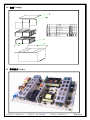
Main Electric Components
(1). MODULE:
There are 1 pc. panel and 3 pcs. PCB including 1 pc. INVERTER
board(L), 1 pc. INVERTER board(R),1 pc. T-CONTROL board,
(2).SIGNAL PROCESS
There are 3 pcs. PCBs including
1 pc. Main digital board, With Tuner board Ass'y
1 pc. Keypad board,
1 pc. Remote Control Receiver board
(3).POWER
There are 1 pc. PCB for power.
33
3&%IXQFWLRQ
3RZHUERDUG
,QSXWYROWDJH$&9a9a+]
,QSXWUDQJH$&90LQa90D[DXWRUHJXODWLRQ
7RSURYLGHSRZHUIRU3&%V
D9IRU,QYHUWHU
E9VEIRUVWDQGE\
F9IRUVLJQDOSRZHU
G9IRU$XGLR$PSSRZHU
H9IRU7XQHUSRZHUDQG/&'SDQQHO
0DLQ9LGHR,QWHU)DFHERDUG
'HFRGHUWKHYLGHRVLJQDO79&9%669,'(2IURPDQDORJWRGLJLWDO
VLJQDO
&RQYHUWHUWKH9LGHRVLJQDOV79&9%669,'(2DQGJUDSKLFVVLJQDO
+'0,9*$<3E3UIURPLQWHUQDFHWRSURJUHVVLYH
&RQYHUWHUWKH'LJLWDOWRILWWKHSDQHOGLVSOD\PRGHDQGRXWSXWWKH
/9'6VLJQDOWR3DQHO
&RQYHUWHUWKH79LQSXWVLJQDOIURP,)WRYLGHRDQG6,)VLJQDO
&RQYHUWHUWKHGLJLWDODQGDQDORJDXGLRVLJQDOWRWRQHFRQWUROOHG
VLJQDOWRDXGLR$03),/(5
.(<ERDUG
7RJHWWKHPDLQEXWWRQFRQWURORQ/&'B79DV
6285&(0(18&+$1(/&+$1(/92/92/67$1'%<IXQFWLRQV
5HPRWH&RQWUROERDUG
5HFHLYHWKHUHPRWHVLJQDODQGDFWLYHIRUWKHFRQWURO
7&21752/ERDUG
&RQYHUWHUWKH/9'6VLJQDOWRWKHGLJLWDOVLJQDOIRUILWWLQJWKH3$1(/
,19(57(5ERDUG
&RQYHUWHUWKHORZ'&YROWDJH9WRKLJK$&YROWDJHWRGULYHWKH
EDFNOLJKW
34
PCB failure analysis
1. CONTROL:
a. Abnormal noise on screen.
b. No picture.
2. MAIN (VIDEO):
a. Lacking color, Bad color scale.
b. No voice.
c. No picture but with signals output, OSD and back light.
d. Abnormal noise on screen.
3. POWER:
No picture, no power output.
Basic operation of LCD-TV
1. After turning on power switch, power board sends 5Vst-by Volt to Micro
Processor IC waiting for ON signals from Key Switch or Remote Receiver.
2. When the ON signal from Key Switch or Remote Receiver is detected, Micro
Processor will send ON Control signals to Power. Then Power sends (5Vsc,
12Vsc, 24V and RLY ON, Vs ON) to PCBs working. This time VIF will send
signals to display back light, OSD on the panel and start to search available
signal sources. If the audio signals input, them will be amplified by Audio AMP
and transmitted to Speakers.
3. If some abnormal signals are detected (for example: over volts, over current,
over temperature and under volts), the system will be shut down by Power off.
35
/&'EDVLFGLVSOD\WKHRU\
When an electrical field is applied to the LC planes, the LC molecules re-align
themselves so that they are parallel to the electrical field. This electrical process
is known as twisted nematic field effect or TNFE. In this alignment, polarized
light is not twisted as it passes through the LC material (see Diagram 3A and
3B). If the front polarizer is oriented perpendicular to the rear polarizer, light will
pass through the energized display but will be blocked by the rear polarizer. An
LCD in this form is acting as a light shutter.
Displays with variable characters are created by selectively etching away the
conductive surface that was originally deposited on the glass. Etched areas
become the display’s background; unetched areas become the display’s
characters.
'LDJUDP$7KHĀRIIāVWDWHRID71/&'WKH/&PROHFXOHVIRUPDWZLVWDQGWKHUHIRUH
FDXVHSRODUL]HGOLJKWWRWZLVWDVLWSDVVHVWKURXJK
'LDJUDP%7KHĀRQāVWDWHWKHHOHFWULFDOILHOGUHDOLJQVWKH/&PROHFXOHVVRWKH\GR
QRWWZLVWWKHSRODUL]HGOLJKW
36
Simple Troubleshooting
If the display fails or the performance changes dramatically, check the Display
in accordance with the following instructions. Remember to check the
peripherals to pinpoint the source of the failure.
Symptom
Solution
Power cannot be turned -Check that both ends of the power cable are
on.(Power indicator
plugged into the socket appropriately and the wall
does not light.)
socket is operational.
No Input Signal
-Check that the signal line is connected properly.
message appears.
-Check that the power of the relevant peripherals is
turned on.
-Check that the Input option that has been selected
matches with the input signal.
The remote control does -Check the batteries are not drained.(Use new
not function properly.
batteries.)
-Check that the remote control is within the operating
range.
-Check that the remote control is pointed to the
remote control window on the display.
-Check that there are no obstacles between the
remote control and the remote control window.
Flashing spots or stripes -Check that there are no emission (Car, HV cable or
appear on the screen.
Neon lamp) or other possible interference sources.
Image colour or quality -Check that all the video settings are adjusted
deteriorates.
appropriately, such as brightness, contrast, colour
etc.
-For more information about video settings, refer to
OSD Functions in Chapter 2.
Screen position and
-Check that the screen position and size is adjusted
size are incorrect.
appropriately.
Image or colour is
-Check that the signal line is connected properly.
incorrect.
-When connecting to a PC, you can change the
resolution of the PC to acquire the correct image.
The discrepancy of the PC output signal may affect
the display of the image.
Display warning
&KHFNWKDWWKHLQSXWVLJQDOOLQHLVSURSHUO\¿[HG
message.
-Select the correct input signal.
-For more information, refer to Supported Signal
Modes in Chapter 4.
37
FACTORY MODE INSTRUSTION:
1. Enter into foctory mode.
In TV normal mode ,Press key “ S.MODE, 5,8,0 ”will go into factory mode。
Select the item by “Up” and “Down” keys, Adjust by “Left” and “Right“ keys, Press
“MENU” key to exit factory mode!
2. Factory mode function.
a. SHOP OUT and HEAT RUN function: This two mode is for factory production. After
writing into the Flash data, should shop out the EEROM data and HEAT RUN for
mass production.
Enter into factory mode and go into OPTION item, Press LEFT of remote
control to use SHOP OUT, the power LED will flash for about 5 seconds, the TV will
auto power down when complete. Power again will be normal.
Enter into factory mode and select HEAT RUN item, Press LEFT of remote
control to HEAT RUN, The TV set will display 7 pure color picture circulate, Only
Press the STANDARDBY key of the front key board can go back to normal mode.
b. Other factory setting and function.
FACTORY MODE
SOURCE
TV
ADC ADJ
AV
S-VIDEO
YPbPr
VGA
YPbPr
VGA
R OFF
127
127
G OFF
127
127
B OFF
127
127
R GAIN
78
78
G GAIN
69
69
B GAIN
78
78
SOFT
STANDARD
BRIGHT
CONTRAST
50
60
70
BRIGHTNESS
40
50
60
HUE
50
50
50
SATURATION
40
50
50
SHARPNESS
40
50
50
NEWS
MUSIC
STANDARD
BASS
40
75
50
TREBLE
70
75
50
NORMAL
WARM
COOL
R OFF
10
10
10
G OFF
10
10
10
B OFF
10
10
10
HDMI
For design
using。
AUTOTUNE
PIC MODE
SND MODE
COL TEMP
Set the value
of different
picture mode
38
R GAIN
103
117
123
G GAIN
108
114
129
B GAIN
115
110
129
NON LINEAR
For design
using.
White
balance
setting.
X0
X1
X2
X3
X4
VOL
0
25
50
75
100
BASS
0
25
50
75
100
TREBLE
0
25
50
75
100
SD.CON
80
100
120
140
160
SD.BRI
18
63
109
154
200
SD.HUE
0
25
50
75
100
SD.SAT
0
63
127
191
255
SD.SHP
0
5
10
15
20
PC.CON
80
113
147
180
214
PC.BRI
18
57
96
135
174
SSC SETTING
MEMORY CLOCK SSC
MODURATION 21
PERCENTAGE 0
PANNEL CLOCK SSC
MODURATION 1
PERCENTAGE 0
EEPROM:
ADDR
00
DATA
00
SAVE
OPTION:
HDCP KEY
0007A124A5F0
SHOP OUT
PRESET CHANNEL
HEAT RUN
S5
RW_
AU2601_
0U
C_
02
(CHASSIS)
(MARKET
AREA)
(PANNEL)
(LOGO)
(LANGUAGE)
VERSION
VERSION
V2.51
15:37:49
01/19/08
(TIME)
39
MST6E16GS
Full HD LCD TV Controller with PIP and VIF
Preliminary Data Sheet Version 0.4
Attention Please: Under the technology license agreement between MStar and Dolby/SRS/BBE, MStar is obliged not to
provide samples that incorporate Dolby/SRS/BBE technology to any third party who is not a qualified licensee of
Dolby/SRS/BBE respectively.
FEATURES
Ÿ
Ÿ
Ÿ
Ÿ
Ÿ
Ÿ
Ÿ
Ÿ
Ÿ
Ÿ
Ÿ
Ÿ
Ÿ
Ÿ
Ÿ
Ÿ
Ÿ
n
n
LCD TV controller with PIP display functions
Input supports up to UXGA & 1080P
Panel supports up to full HD (1920x1080)
TV decoder with 3-D comb filter
Multi-standard TV sound demodulator and
decoder
10-bit triple-ADC for TV and RGB/YPbPr
10-bit video data processing
Integrated DVI/HDCP/HDMI compliant
receiver
High-quality dual scaling engines & dual 3-D video
de-interlacers
3-D video noise reduction
MStarACE-3 picture/color processing engine
Embedded On-Screen Display (OSD) controller
engine
Built-in MCU supports PWM & GPIO
Built-in dual-link 8/10-bit LVDS transmitter
5-volt tolerant inputs
Low EMI and power saving features
216-pin LQFP
NTSC/PAL/SECAM Video Decoder
Ÿ Supports NTSC M, NTSC-J, NTSC-4.43, PAL
(B,D,G,H,M,N,I,Nc), and SECAM
Ÿ Automatic TV standard detection
Ÿ 3-D Comb filter for NTSC/PAL
Ÿ 5 configurable CVBS & Y/C S-video inputs
Ÿ Supports Teletext level-1.5, WSS, VPS,
Closed-caption, and V-chip
Ÿ CVBS video output
Video IF for Multi-Standard Analog TV
Ÿ Digital low IF architecture
Ÿ Stepped-gain PGA with 26 dB tuning range
and 1 dB tuning resolution
Ÿ Maximum IF analog gain of 37dB in addition to
digital gain
Ÿ Programmable TOP to accommodate different
tuner gain to optimize noise and linearity
performance
Version 0.4
n
n
n
n
1
2
3
Multi-Standard TV Sound Decoder
Ÿ Supports BTSC/NICAM/A2/EIA-J demodulation
and decoding
Ÿ FM stereo & SAP demodulation
Ÿ L/Rx2 and SIF audio inputs
Ÿ L/Rx2 loudspeaker and line outputs
Ÿ Supports sub-woofer output
Ÿ Built-in audio output DAC’s
Ÿ Audio processing for loudspeaker channel,
including volume, balance, mute, tone, and
P/G EQ
Ÿ Support MP3 decode
Ÿ Optional advanced surround available
(Dolby1, SRS2, BBE3… etc) Note
Digital Audio Interface
Ÿ S/PDIF digital audio input & output
Ÿ HDMI audio channel processing capability
Ÿ Programmable delay for audio/video
synchronization
Analog RGB Compliant Input Ports
Ÿ Two analog ports support up to UXGA
Ÿ Fast blanking and function selection switch
support full SCART functions
Ÿ Supports HDTV RGB/YPbPr/YCbCr
Ÿ Supports Composite Sync and SOG
(Sync-on-Green) separator
Ÿ Automatic color calibration
DVI/HDCP/HDMI Compliant Input Port
Ÿ Two DVI/HDMI input ports with built-in switch
Ÿ Supports TMDS clock up to 225MHz @ 1080P
60Hz with 12-bit deep-color resolution
Ÿ Single link on-chip DVI 1.0 compliant receiver
Ÿ High-bandwidth Digital Content Protection
(HDCP) 1.1 compliant receiver
Ÿ High Definition Multimedia Interface (HDMI)
1.3 compliant receiver with CEC support
Trademark of Dolby Laboratories
Trademark of SRS Labs, Inc.
Registered trademark of BBE Sound, Inc.
-1Copyright © 2008 MStar Semiconductor, Inc. All rights reserved.
10/7/2008
MST6E16GS
Full HD LCD TV Controller with PIP and VIF
Preliminary Data Sheet Version 0.4
n
n
n
Ÿ Long-cable tolerant robust receiving
Ÿ Support HDTV up to 1080P
Auto-Configuration/Auto-Detection
Ÿ Auto input signal format and mode detection
Ÿ Auto-tuning function including phasing,
positioning, offset, gain, and jitter detection
Ÿ Sync detection for H/V Sync
High-Performance Scaling Engines
Ÿ Fully programmable shrink/zoom capabilities
Ÿ Nonlinear video scaling supports various
modes including Panorama
Video Processing & Conversion
Ÿ 3-D motion adaptive video de-interlacer
Ÿ Edge-oriented adaptive algorithm for smooth
low-angle edges
Ÿ Automatic 3:2 pull-down & 2:2 pull-down
detection and recovery
Ÿ PIP with programmable size and location,
supports multi-video applications
Ÿ MStar 3rd Generation Advanced Color Engine
(MStarACE-3) automatic picture enhancement
gives:
Ÿ Brilliant and fresh color
Ÿ Intensified contrast and details
Ÿ Vivid skin tone
Ÿ Sharp edge
Ÿ Enhanced depth of field perception
Ÿ Accurate and independent color control
Ÿ sRGB compliance allows end-user to
experience the same colors as viewed on CRTs
and other displays
Ÿ Programmable 12-bit RGB gamma CLUT
Ÿ 3-D video noise reduction
Ÿ Frame rate conversion
Version 0.4
n
n
n
n
On-Screen OSD Controller
Ÿ 16/256 color palette
Ÿ 512 1/2/4/8-bit per pixel fonts
Ÿ Supports texture function
Ÿ Supports 4K attribute/code
Ÿ Horizontal and vertical stretch of OSD menus
Ÿ Pattern generator for production test
Ÿ Supports OSD MUX and alpha blending
capability
Ÿ Supports blinking and scrolling for closed
caption applications
LVDS Panel Interface
Ÿ Supports 8/10-bit dual link LVDS up to full HD
(1920x1080)
Ÿ Supports 2 data output formats: Thine & TI
data mappings
Ÿ Compatible with TIA/EIA
Ÿ Dithering with 6/8 bits options
Ÿ Reduced swing for LVDS for low EMI
Ÿ Supports flexible spread spectrum frequency
with 360Hz~11.8MHz and up to 25%
modulation
Integrated Micro Controller
Ÿ Embedded 8032 micro controller
Ÿ Configurable PWM’s and GPIO’s
Ÿ Low-speed ADC inputs for system control
Ÿ SPI bus for external flash
Ÿ Supports external MCU option controlled
through 4-wire double-data-rate direct MCU
bus
External Connection/Component
Ÿ USB 2.0 port with internal switch to host
controller
Ÿ 16-bit data bus for external frame buffer (DDR
DRAM)
Ÿ All system clocks synthesized from a single
external clock
-2Copyright © 2008 MStar Semiconductor, Inc. All rights reserved.
10/7/2008
MST6E16GS
Full HD LCD TV Controller with PIP and VIF
Preliminary Data Sheet Version 0.4
GENERAL DESCRIPTION
The MST6E16GS is a high performance and fully integrated IC for multi-function LCD monitor/TV with
resolutions up to full HD (1920x1080). It is configured with an integrated triple-ADC/PLL, an integrated
DVI/HDCP/HDMI receiver, a multi-standard TV video and audio decoder, a video de-interlacer, a scaling engine,
the MStarACE-3 color engine, an on-screen display controller, an 8-bit MCU and a built-in output panel interface.
By use of external frame buffer, PIP/POP is provided for multimedia applications. Furthermore, 3-D video
decoding and processing are fulfilled for high-quality TV applications. To further reduce system costs, the
MST6E16GS also integrates intelligent power management control capability for green-mode requirements and
spread-spectrum support for EMI management.
Version 0.4
-3Copyright © 2008 MStar Semiconductor, Inc. All rights reserved.
10/7/2008
MST6E16GS
Full HD LCD TV Controller with PIP and VIF
Preliminary Data Sheet Version 0.4
163
164
165
166
167
168
169
170
171
172
173
174
175
176
177
178
179
180
181
182
183
184
185
186
187
188
189
190
191
192
193
194
195
196
197
198
199
200
201
202
203
204
205
206
207
210
209
208
211
212
213
214
1
162
2
161
Pin 1
3
160
4
159
5
158
6
7
157
156
8
155
154
153
11
152
12
151
13
150
14
149
15
148
16
147
17
146
18
145
19
144
20
143
21
142
22
141
23
140
24
139
25
138
26
137
27
28
29
30
31
32
33
34
35
36
37
38
39
40
41
MST6E16GS-LF
9
10
XXXXXXXX
XXXXX
136
135
134
133
132
131
130
129
128
127
126
125
124
123
122
42
121
43
120
44
119
45
118
46
117
47
116
48
115
108
107
106
105
104
103
102
101
99
100
98
97
96
95
94
93
92
91
90
89
88
87
86
85
84
83
82
81
80
79
78
77
76
75
74
73
72
71
70
69
68
67
66
65
64
INT
DDCA_SCL
DDCA_SDA
DDCR_SCL
DDCR_SDA
PWM1
PWM0
SAR3
SAR2
SAR1
SAR0
VDDC
GND
SPI_SDO
SPI_SCZ
SPI_SDI
SPI_SCK
VDDP
GND
USB20_DP
USB20_DM
AVDD_USB
USB20_REXT
MVREF
MCLKE
MCLK
MCLKZ
DQM1
DQS1
AVDD_MI
MDATA[15]
MDATA[14]
MDATA[13]
MDATA[12]
AVDD_MI
MDATA[11]
MDATA[10]
GND
MDATA[9]
MDATA[8]
AVDD_MI
MDATA[7]
MDATA[6]
MDATA[5]
MDATA[4]
AVDD_MI
MDATA[3]
MDATA[2]
GND
MDATA[1]
MDATA[0]
AVDD_MI
DQS0
DQM0
TAGC
AVDD_AU
GND
AUVRM
AUVRP
AUVAG
AVDD_AU
LINE_IN_0L
LINE_IN_0R
LINE_IN_1L
LINE_IN_1R
AUCOM
LINE_OUT_3L
LINE_OUT_3R
LINE_OUT_2L
LINE_OUT_2R
LINE_OUT_1L
LINE_OUT_1R
GPIOD[0]
GPIOD[1]
GPIOD[2]
VDDP
GND
VDDC
AD[0]
AD[1]
AD[2]
AD[3]
WRZ
RDZ
ALE
BADR[1]
BADR[0]
RASZ
VDDC
GND
AVDD_MI
CASZ
WEZ
MADR[11]
MADR[10]
MADR[9]
MADR[8]
MADR[7]
MADR[6]
MADR[5]
MADR[4]
MADR[3]
MADR[2]
MADR[1]
MADR[0]
GND
AVDD_MI
AVDD_MIPLL
63
109
62
110
54
61
111
53
60
112
52
59
51
58
113
57
114
50
56
49
55
RXACKN
RXACKP
RXA0N
RXA0P
AVDD_33
RXA1N
RXA1P
RXA2N
RXA2P
HPLUGA
REXT
DDCDA_SDA
DDCDA_SCL
VCLAMP
REFP
REFM
BIN1P
SOGIN1
GIN1P
RIN1P
BIN0M
BIN0P
GIN0M
GIN0P
SOGIN0
RIN0P
AVDD_33
GND
HSYNC0
VSYNC0
VSYNC2
Y0
CVBS3
CVBS2
CVBS1
VCOM1
CVBS0
VCOM0
AVDD_33
CVBSOUT1
CVBSOUT0
GND
XOUT
XIN
AVDD_MPLL
GND_VIFPLL
VR27
AVDD_RXS
GND_RXS
SIFP
SIFM
VIFM
VIFP
AVDD_RXV
215
216
DDCDB_SCL
DDCDB_SDA
HPLUGB
RXB2P
RXB2N
GND
RXB1P
RXB1N
GND
RXB0P
RXB0N
AVDD_33
RXBCKP
RXBCKN
VDDC
GPIOM[1]
GPIOM[0]
GND
VDDP
LVB0M
LVB0P
LVB1M
LVB1P
LVB2M
LVB2P
LVBCKM
LVBCKP
LVB3M
LVB3P
LVB4M
LVB4P
GND
VDDP
LVA0M
LVA0P
LVA1M
LVA1P
LVA2M
LVA2P
LVACKM
LVACKP
LVA3M
LVA3P
LVA4M
LVA4P
VDDC
GND
HWRESET
GPIOT[1]
VDDP
PWM3
PWM2
VDDP
IRIN
PIN DIAGRAM (MST6E16GS)
Version 0.4
-4Copyright © 2008 MStar Semiconductor, Inc. All rights reserved.
10/7/2008
MST6E16GS
Full HD LCD TV Controller with PIP and VIF
Preliminary Data Sheet Version 0.4
PIN DESCRIPTION
MCU Interface
Pin Name
Pin Type
Function
Pin
AD[3]
I/O w/5V-tolerant
MCU 4-bit DDR Direct Bus; 4mA driving strength
82
AD[2:0]
I/O (not 5V-tolerant)
MCU 4-bit DDR Direct Bus; 4mA driving strength
81-79
WRZ
I/O w/ 5V-tolerant
MCU Bus WDZ, active low
83
RDZ
I/O w/ 5V-tolerant
MCU Bus RDZ, active
84
ALE
I/O w/ 5V-tolerant
MCU Bus ALE, active high
85
SPI_SCK
Output (not 5V-tolerant) SPI Flash Serial Clock
146
SPI_SDI
Output (not 5V-tolerant) SPI Flash Serial Data Input
147
SPI_SCZ
Output (not 5V-tolerant) SPI Flash Chip Select
148
SPI_SDO
Input w/ 5V-tolerant
SPI Flash Serial Data Output
149
INT
I/O w/ 5V-tolerant
External Interrupt Input/Output
162
HWRESET
Schmitt Trigger Input
w/ 5V-tolerant
Hardware Reset; active high
169
Analog Video Interface
Pin Name
Pin Type
Function
Pin
REXT
Analog Input
External Resister 390 ohm to AVDD_33
11
VCLAMP
CVBS/YC Mode Clamp Voltage Bypass
14
REFP
Internal ADC Reference Top De-coupling Pin
15
REFM
Internal ADC Reference Bottom De-coupling Pin
16
HSYNC0
Schmitt Trigger Input
w/ 5V-tolerant
Analog HSYNC Input from Channel 0
29
VSYNC0
Schmitt Trigger Input
w/ 5V-tolerant
Analog VSYNC Input from Channel 0
30
BIN0M
Analog Input
Reference Ground for Analog Blue Input from Channel 0
21
BIN0P
Analog Input
Analog Blue Input from Channel 0
22
GIN0M
Analog Input
Reference Ground for Analog Green Input from Channel 0
23
GIN0P
Analog Input
Analog Green Input from Channel 0
24
SOGIN0
Analog Input
Sync-On-Green Input from Channel 0
25
RIN0P
Analog Input
Analog Red Input from Channel 0
26
BIN1P
Analog Input
Analog Blue Input from Channel 1
17
SOGIN1
Analog Input
Sync-On-Green Input from Channel 1
18
GIN1P
Analog Input
Analog Green Input from Channel 1
19
Version 0.4
-5Copyright © 2008 MStar Semiconductor, Inc. All rights reserved.
10/7/2008
MST6E16GS
Full HD LCD TV Controller with PIP and VIF
Preliminary Data Sheet Version 0.4
Pin Name
Pin Type
Function
Pin
RIN1P
Analog Input
Analog Red Input from Channel 1
20
VSYNC2
Schmitt Trigger Input
w/ 5V-tolerant
Analog VSYNC Input from Channel 2
31
Y0
Analog Input
Luma Video Input 0 /
CVBS Input Channel 4 (CVBS4)
32
CVBS3
Analog Input
Analog CVBS (Composite) / S-Video (Y/C) Input Channel 3 33
CVBS2
Analog Input
Analog CVBS (Composite) / S-Video (Y/C) Input Channel 2 34
CVBS1
Analog Input
Analog CVBS (Composite) / S-Video (Y/C) Input Channel 1 35
CVBS0
Analog Input
Analog CVBS (Composite) / S-Video (Y/C) Input Channel 0 37
VCOM1
Analog Input
Common Analog Input Reference Ground 1 (for
CVBS/ADCB)
36
VCOM0
Analog Input
Common Analog Input Reference Ground 0 (for
CVBS/ADCB)
38
CVBSOUT1
Analog Output
CVBS (Composite) Video Output Channel 1
40
CVBSOUT0
Analog Output
CVBS (Composite) Video Output Channel 0
41
Analog Audio Interface
Pin Name
Pin Type
Function
Pin
AUVRM
Analog Output
Negative Reference Voltage for Audio ADC
58
AUVRP
Analog Output
Positive Reference Voltage for Audio ADC
59
AUVAG
Analog Output
Reference Voltage for Audio Common Mode
60
LINE_IN_0L
Analog Input
Audio Line Input Left Channel 0
62
LINE_IN_0R
Analog Input
Audio Line Input Right Channel 0
63
LINE_IN_1L
Analog Input
Audio Line Input Left Channel 1
64
LINE_IN_1R
Analog Input
Audio Line Input Right Channel 1
65
AUCOM
Analog Input
Reference Ground for Audio Line Input
66
LINE_OUT_1L
Analog Output
Main Audio Output Left Channel 1 (DA0)
71
LINE_OUT_1R
Analog Output
Main Audio Output Right Channel 1 (DA0)
72
LINE_OUT_2L
Analog Output
Main Audio Output Left Channel 2 (AA1)
69
LINE_OUT_2R
Analog Output
Main Audio Output Right Channel 2 (AA1)
70
LINE_OUT_3L
Analog Output
Main Audio Output Left Channel 3 (AA0)
67
LINE_OUT_3R
Analog Output
Main Audio Output Right Channel 3 (AA0)
68
Version 0.4
-6Copyright © 2008 MStar Semiconductor, Inc. All rights reserved.
10/7/2008
MST6E16GS
Full HD LCD TV Controller with PIP and VIF
Preliminary Data Sheet Version 0.4
DVI/HDMI Interface
Pin Name
Pin Type
Function
Pin
RXACKN
DVI/HDMI Input
Negative DVI/HDMI Input for A Link Clock Channel
1
RXACKP
DVI/HDMI Input
Positive DVI/HDMI Input for A Link Clock Channel
2
RXA0N
DVI/HDMI Input
Negative DVI/HDMI Input for A Link Data Channel 0
3
RXA0P
DVI/HDMI Input
Positive DVI/HDMI Input for A Link Data Channel 0
4
RXA1N
DVI/HDMI Input
Negative DVI/HDMI Input for A Link Data Channel 1
6
RXA1P
DVI/HDMI Input
Positive DVI/HDMI Input for A Link Data Channel 1
7
RXA2N
DVI/HDMI Input
Negative DVI/HDMI Input for A Link Data Channel 2
8
RXA2P
DVI/HDMI Input
Positive DVI/HDMI Input for A Link Data Channel 2
9
RXBCKN
DVI/HDMI Input
Negative DVI/HDMI Input for B Link Clock Channel
203
RXBCKP
DVI/HDMI Input
Positive DVI/HDMI Input for B Link Clock Channel
204
RXB0N
DVI/HDMI Input
Negative DVI/HDMI Input for B Link Data Channel 0
206
RXB0P
DVI/HDMI Input
Positive DVI/HDMI Input for B Link Data Channel 0
207
RXB1N
DVI/HDMI Input
Negative DVI/HDMI Input for B Link Data Channel 1
209
RXB1P
DVI/HDMI Input
Positive DVI/HDMI Input for B Link Data Channel 1
210
RXB2N
DVI/HDMI Input
Negative DVI/HDMI Input for B Link Data Channel 2
212
RXB2P
DVI/HDMI Input
Positive DVI/HDMI Input for B Link Data Channel 2
213
LVDS Interface
Pin Name
Pin Type
Function
Pin
LVA0M
Output
LVDS A-Link Channel 0 Negative Data Output
183
LVA0P
Output
LVDS A-Link Channel 0 Positive Data Output
182
LVA1M
Output
LVDS A-Link Channel 1 Negative Data Output
181
LVA1P
Output
LVDS A-Link Channel 1 Positive Data Output
180
LVA2M
Output
LVDS A-Link Channel 2 Negative Data Output
179
LVA2P
Output
LVDS A-Link Channel 2 Positive Data Output
178
LVA3M
Output
LVDS A-Link Channel 3 Negative Data Output
175
LVA3P
Output
LVDS A-Link Channel 3 Positive Data Output
174
LVA4M
Output
LVDS A-Link Channel 4 Negative Data Output
173
LVA4P
Output
LVDS A-Link Channel 4 Positive Data Output
172
LVACKM
Output
LVDS A-Link Negative Clock Output
177
LVACKP
Output
LVDS A-Link Positive Clock Output
176
LVB0M
Output
LVDS B-Link Channel 0 Negative Data Output
197
Version 0.4
-7Copyright © 2008 MStar Semiconductor, Inc. All rights reserved.
10/7/2008
MST6E16GS
Full HD LCD TV Controller with PIP and VIF
Preliminary Data Sheet Version 0.4
Pin Name
Pin Type
Function
Pin
LVB0P
Output
LVDS B-Link Channel 0 Positive Data Output
196
LVB1M
Output
LVDS B-Link Channel 1 Negative Data Output
195
LVB1P
Output
LVDS B-Link Channel 1 Positive Data Output
194
LVB2M
Output
LVDS B-Link Channel 2 Negative Data Output
193
LVB2P
Output
LVDS B-Link Channel 2 Positive Data Output
192
LVB3M
Output
LVDS B-Link Channel 3 Negative Data Output
189
LVB3P
Output
LVDS B-Link Channel 3 Positive Data Output
188
LVB4M
Output
LVDS B-Link Channel 4 Negative Data Output
187
LVB4P
Output
LVDS B-Link Channel 4 Positive Data Output
186
LVBCKM
Output
LVDS B-Link Negative Clock Output
191
LVBCKP
Output
LVDS B-Link Positive Clock Output
190
GPIO Interface
Pin Name
Pin Type
Function
Pin
GPIOD[2:0]
I/O (not 5V-tolerant)
General Purpose Input/Output
75-73
GPIOT[1]
I/O w/ 5V-tolerant
General Purpose Input/Output
168
GPIOM[1:0]
I/O w/ 5V-tolerant
General Purpose Input/Output
201, 200
SAR0
I/O (not 5V-tolerant)
SAR Low Speed ADC Input 0
152
SAR1
I/O (not 5V-tolerant)
SAR Low Speed ADC Input 1
153
SAR2
I/O (not 5V-tolerant)
SAR Low Speed ADC Input 2
154
SAR3
I/O (not 5V-tolerant)
SAR Low Speed ADC Input 3
155
PWM0
I/O (not 5V-tolerant)
Pulse Width Modulation Output; 4mA driving strength /
MCU Configuration Input 0 During Reset /
General Purpose Input/Output
156
PWM1
I/O (not 5V-tolerant)
Pulse Width Modulation Output; 4mA driving strength /
MCU Configuration Input 1 During Reset /
General Purpose Input/Output
157
PWM2
I/O (not 5V-tolerant)
Pulse Width Modulation Output; 4mA driving strength /
General Purpose Input/Output
165
PWM3
I/O (not 5V-tolerant)
Pulse Width Modulation Output; 4mA driving strength /
General Purpose Input/Output
166
IRIN
Input w/5V-tolerant
IR Receiver Input /
General Purpose Input/Output
163
Version 0.4
-8Copyright © 2008 MStar Semiconductor, Inc. All rights reserved.
10/7/2008
MST6E16GS
Full HD LCD TV Controller with PIP and VIF
Preliminary Data Sheet Version 0.4
DRAM Interface
Pin Name
Pin Type
Function
Pin
BADR[1:0]
Output
DRAM Memory Bank Address
86, 87
RASZ
Output
Row Address Strobe; active low
88
CASZ
Output
Column Address Strobe; active low
92
WEZ
Output
Write Enable; active low
93
MADR[11:0]
Output
DRAM Memory Address
94-105
DQM[1:0]
Output
Data Mask for Low Byte; active high
135, 109
DQS[1:0]
I/O
Data Strobe
134, 110
MDATA[15:0]
I/O
DRAM Memory Data Bus
132-129, 127,
126, 124, 123,
121-118, 116,
115, 113, 112
MCLKZ
Output
DRAM Memory Negative Differential Clock
136
MCLK
Output
DRAM Memory Positive Differential Clock
137
MCLKE
Output
DRAM Memory Clock Enable
138
MVREF
Input
Reference Voltage for DDR SDRAM Interface
139
USB Interface
Pin Name
Pin Type
USB20_REXT
Function
Pin
USB External Resistor Pin; Connected through 900 ohm
(±1%) Resistor to GND
140
USB20_DM
Analog I/O
USB 2.0 Inverting Data Input/Output
142
USB20_DP
Analog I/O
USB 2.0 Non-inverting Data Input/Output
143
Function
Pin
Compensation Capacitor for Regulator
46
VIF Interface
Pin Name
Pin Type
VR27
SIFP
Analog Input
Positive Sound IF Input
49
SIFM
Analog Input
Negative Sound IF Input
50
VIFM
Analog Input
Negative Video IF Input
51
VIFP
Analog Input
Positive Video IF Input
52
TAGC
Analog Output
Tuner Automatic Gain Control Output
55
Version 0.4
-9Copyright © 2008 MStar Semiconductor, Inc. All rights reserved.
10/7/2008
MST6E16GS
Full HD LCD TV Controller with PIP and VIF
Preliminary Data Sheet Version 0.4
Misc Interface
Pin Name
Pin Type
Function
Pin
XOUT
Analog Output
Crystal Oscillator Output
43
XIN
Analog Input
Crystal Oscillator Input
44
DDCR_SDA
I/O w/ 5V-tolerant
DDC Data for ROM
158
DDCR_SCL
I/O w/ 5V-tolerant
DDC Clock for ROM
159
DDCA_SDA
I/O w/ 5V-tolerant
DDC Data for Analog Interface; 4mA driving strength
160
DDCA_SCL
Input w/ 5V-Tolerant
DDC Clock for Analog Interface
161
HPLUGA
I/O w/ 5V-tolerant
Hot-plug control for DVI/HDMI Port A
10
HPLUGB
I/O w/ 5V-tolerant
Hot-plug control for DVI/HDMI Port B
214
DDCDA_SDA
I/O w/ 5V-Tolerant
DDC Data and HDCP Slave Serial Bus Data I/O for
DVI/HDMI Port A; 4mA driving strength
12
DDCDA_SCL
Input w/ 5V-tolerant
DDC Clock and HDCP Slave Serial Bus Clock Input for
DVI/HDMI Port A
13
DDCDB_SDA
I/O w/ 5V-Tolerant
DDC Data and HDCP Slave Serial Bus Data I/O for
DVI/HDMI Port B; 4mA driving strength
215
DDCDB_SCL
Input w/ 5V-tolerant
DDC Clock and HDCP Slave Serial Bus Clock Input for
DVI/HDMI Port B
216
Pin Name
Pin Type
Function
Pin
AVDD_33
3.3V Power
Analog Power
5, 27, 39, 205
AVDD_MPLL
3.3V Power
MPLL Power
45
AVDD_RXS
3.3V Power
Sound Path Receiver Power
48
GND_RXS
Ground
Sound Path Receiver Ground
49
GND_RXV
Ground
Video Path Receiver Ground
53
AVDD_RXV
3.3V Power
Video Path Receiver Power
54
AVDD_AU
3.3V Power
Audio Power
56, 61
AVDD_MI
2.5V Power
Memory Interface Power
91, 107, 111, 117, 122, 128, 133
AVDD_MIPLL
3.3V Power
Memory Interface PLL Power
108
AVDD_USB
3.3V Power
USB Power
141
VDDC
1.26V Power
Digital Core Power
78, 89, 151, 171, 202
VDDP
3.3V Power
Digital Input/Output Power
76, 145, 164, 167, 184, 198
GND
Ground
Ground
28, 42, 57, 77, 90, 106, 114, 125,
144, 150, 170, 185, 199, 208, 211
Power Pins
Version 0.4
- 10 Copyright © 2008 MStar Semiconductor, Inc. All rights reserved.
10/7/2008
MST6E16GS
Full HD LCD TV Controller with PIP and VIF
Preliminary Data Sheet Version 0.4
ELECTRICAL SPECIFICATIONS
Analog Interface Characteristics
Parameter
Min
VIDEO ADC Resolution
Typ
Max
10
Unit
Bits
DC ACCURACY
Differential Nonlinearity
TBD
Integral Nonlinearity
TBD
TBD
LSB
LSB
VIDEO ANALOG INPUT
Input Voltage Range
Minimum
0.5
Maximum
1.0
V p-p
V p-p
Input Bias Current
1
uA
Input Full-Scale Matching
1.5
%FS
Brightness Level Adjustment
62
%FS
SWITCHING PERFORMANCE
Maximum Conversion Rate
165
MSPS
Minimum Conversion Rate
12
MSPS
HSYNC Input Frequency
15
200
kHz
PLL Clock Rate
12
165
MHz
PLL Jitter
500
ps p-p
Sampling Phase Tempco
15
ps/°C
250
MHz
DYNAMIC PERFORMANCE
Analog Bandwidth, Full Power
DIGITAL INPUTS
Input Voltage, High (VIH)
2.5
V
Input Voltage, Low (VIL)
0.8
V
Input Current, High (IIH)
-1.0
uA
Input Current, Low (IIL)
1.0
uA
Input Capacitance
5
pF
DIGITAL OUTPUTS
Output Voltage, High (VOH)
VDDP-0.1
V
Output Voltage, Low (VOL)
0.1
V
VIDEO ANALOG OUTPUT
CVBS Buffer Output
Output Low
Output High
Version 0.4
1.5
V
2.0
V
- 11 Copyright © 2008 MStar Semiconductor, Inc. All rights reserved.
10/7/2008
MST6E16GS
Full HD LCD TV Controller with PIP and VIF
Preliminary Data Sheet Version 0.4
Parameter
Min
Typ
Max
Unit
AUDIO
ADC Input
2.0
V p-p
DAC Output
2.0
V p-p
SIF Input Range
Minimum
Maximum
FSSW Input1
SAR ADC Input
FB ADC Input
0.1
V p-p
V p-p
0
1.8
V
0
3.3
V
0
1.25
V
1.0
2
Specifications subject to change without notice.
Notes:
1. Input full scale is typically 1.8V, but input range is 0 ~ 3.3V.
2. Input full scale is 1.25V, but input range is 0 ~ 3.3V.
Absolute Maximum Ratings
Parameter
Symbol
Min
Typ
Max
Units
3.3V Supply Voltages
VVDD_33
3.6
V
2.5V Supply Voltages
VVDD_25
2.75
V
1.26V Supply Voltages
VVDD_126
1.32
V
Input Voltage (5V tolerant inputs)
VIN5Vtol
5.0
V
Input Voltage (non 5V tolerant inputs)
VIN
VVDD_33
V
Ambient Operating Temperature
TA
0
70
°C
Storage Temperature
TSTG
-40
150
°C
Junction Temperature
TJ
150
°C
Note: Stresses above those listed in Absolute Maximum Ratings may cause permanent damage to the device. This is a
stress rating only and does not imply functional operation of the device. Exposure to absolute maximum ratings for
extended periods may affect device reliability.
Version 0.4
- 12 Copyright © 2008 MStar Semiconductor, Inc. All rights reserved.
10/7/2008
MST6E16GS
Full HD LCD TV Controller with PIP and VIF
Preliminary Data Sheet Version 0.4
ORDERING GUIDE
The SRS TruSurround XTTM technology rights incorporated in the
Model
Temperature
Package
Package
Range
Description Option
MST6E16GS
0°C to +70°C
LQFP
216
use of the chip and display of the SRS Labs trademarks. Any
MST6E16GS-LF
0°C to +70°C
LQFP
216
products incorporating the MST6E16GS must be sent to SRS Labs
MST6E16GS-S1
0°C to +70°C
LQFP
216
MST6E16GS-LF-S1
0°C to +70°C
LQFP
216
MST6E16GS-S2
0°C to +70°C
LQFP
216
selected
MST6E16GS-LF-S2
0°C to +70°C
LQFP
216
MST6E16GS, nor the corresponding sale of audio enhancement
MST6E16GS-S3
0°C to +70°C
LQFP
216
MST6E16GS-LF-S3
0°C to +70°C
LQFP
216
MST6E16GS-S4
0°C to +70°C
LQFP
216
MST6E16GS-LF-S4
0°C to +70°C
LQFP
216
MST6E16GS-S5
0°C to +70°C
LQFP
216
MST6E16GS-LF-S5
0°C to +70°C
LQFP
216
Note on product suffix:
1. “LF”: Lead-free version.
2. “S1” ~ “S5”: Advanced surround features.
MST6E16GS are owned by SRS Labs, a U.S. Corporation and
licensed to MStar. Purchaser of MST6E16GS must sign a license for
for review. SRS TruSurround XT is protected under US and foreign
patents issued and/or pending. SRS TruSurround XT, SRS and (O)
symbol are trademarks of SRS Labs, Inc. in the United States and
foreign
countries.
Neither
the
purchase
of
the
equipment conveys the right to sell commercialized recordings
made with any SRS technology. SRS Labs requires all set makers
to comply with all rules and regulations as outlined in the SRS
Trademark Usage Manual separately provided.
Supply of this Implementation of Dolby Technology does not
convey a license nor imply a right under any patent, or any other
Industrial or Intellectual Property Right of Dolby Laboratories, to
use this Implementation in any finished end-user or ready-to-use
final product. Companies planning to use this Implementation in
products must obtain a license from Dolby Laboratories Licensing
Code
Description
S1
SRS TruSurround XTTM
S2
Dolby® ProLogic® II + Dolby® Virtual Speaker
S3
Dolby® ProLogic® II + Virtual Dolby® Surround
S4
BBE®
S5
BBE® ViVATM
Corporation before designing such products.
MARKING INFORMATION
DISCLAIMER
MST6E16GS
MSTAR SEMICONDUCTOR RESERVES THE
RIGHT
TO
MAKE
CHANGES
WITHOUT
FURTHER NOTICE TO ANY PRODUCTS HEREIN
TO IMPROVE RELIABILITY, FUNCTION OR
DESIGN. NO RESPONSIBILITY IS ASSUMED
BY MSTAR SEMICONDUCTOR ARISING OUT OF
THE APPLICATION OR USER OF ANY PRODUCT
OR CIRCUIT DESCRIBED HEREIN; NEITHER
DOES IT CONVEY ANY LICENSE UNDER ITS
PATENT RIGHTS, NOR THE RIGHTS OF
OTHERS.
Part Number
Lot Number
Operation Code A
Operation Code B
Date Code (YYWW)
Electrostatic charges accumulate on both test equipment and human body and can discharge
without detection. MST6E16GS comes with ESD protection circuitry; however, the device may be
permanently damaged when subjected to high energy discharges. The device should be handled
with proper ESD precautions to prevent malfunction and performance degradation.
Version 0.4
- 13 Copyright © 2008 MStar Semiconductor, Inc. All rights reserved.
10/7/2008
MST6E16GS
Full HD LCD TV Controller with PIP and VIF
Preliminary Data Sheet Version 0.4
REVISION HISTORY
Document
Description
Date
MST6E16GS_ds_v01
Ÿ Initial release
Jun 2008
MST6E16GS_ds_v02
Ÿ Added 3-D Comb and Advanced Sound Technology related
information
Ÿ Updated Features / Digital Audio Interface
Ÿ Updated to DDR DRAM in Features
Ÿ Updated Mechanical Dimensions
Jul 2008
MST6E16GS_ds_v03
Ÿ Revised Pin #56 in Pin Diagram and Pin Description
Aug 2008
MST6E16GS_ds_v04
Ÿ Updated Pin 46-53 in Pin Diagram and Pin Description
Ÿ Updated voltage of VDDC pins
Oct 2008
Version 0.4
- 14 Copyright © 2008 MStar Semiconductor, Inc. All rights reserved.
10/7/2008
MST6E16GS
Full HD LCD TV Controller with PIP and VIF
Preliminary Data Sheet Version 0.4
MECHANICAL DIMENSIONS
D
D1
A
A1
E1
E
A2
L1
E-Pad
(at back of IC)
q
c
Seating Plane
b
L
Symbol
Millimeter
e
Inch
Symbol
Min. Nom. Max. Min. Nom. Max.
Millimeter
Min. Nom. Max. Min. Nom. Max.
-
0.063
q
0°
-
-
0.006
L
0.45
0.60
1.45 0.053 0.055 0.057
L1
A
-
-
1.60
-
A1
0.05
-
0.15 0.002
A2
1.35
1.40
Inch
7°
0°
-
7°
0.75 0.018 0.024 0.030
1.00 REF.
0.039 REF.
D
26.00
1.024
b
-
0.18
-
-
0.007
-
D1
24.00
0.945
c
-
0.14
-
-
0.006
-
E
26.00
1.024
e
E1
24.00
0.945
Version 0.4
0.40 BSC
- 15 Copyright © 2008 MStar Semiconductor, Inc. All rights reserved.
0.016 BSC
10/7/2008
Winbond Confidential Information
®
(Do not copy or distribute to unauthorized parties)
2M, 4M AND 8M-BIT SERIAL FLASH MEMORY
W25X20, W25X40 AND W25X80
FEATURES
GENERAL DESCRIPTION
• Family of Serial Flash Memories
– W25X20: 2M-bit / 256K-byte (262,144 ) 1024 pages
– W25X40: 4M-bit /512K-byte (524,288 ) 2048 pages
– W25X80: 8M-bit / 1M-byte (1,048,576 ) 4,096 pages
– 256-bytes per programmable page
– Uniform 4K-byte Sectors and 64K-byte Blocks
The W25X20 (2M-bit), W25X40 (4M-bit) and W25X80 (8Mbit) Serial Flash memories provide a storage solution for
systems with limited space, pins and power. The 25X series
offers flexibility and performance well beyond ordinary
Serial Flash devices. They are ideal for code download
applications as well as storing voice, text and data. The
devices operate on a single 2.7V to 3.6V power supply with
current consumption as low as 5mA active and 1μA for
power-down. All devices are offered in space-saving packages.
• SPI Serial Interface with Single or Dual Outputs
– Clock, Chip Select, Data I/O, Data Out
– Optional Hold function for SPI flexibility
• Fast Data Transfer up to 136M-bits / second
– Clock operation to 68MHz
– Fast Read Dual Output instruction
– Auto-increment Read capability
• Flexable Array Architecture with 4KB sectors
– Sector Erase (4K-bytes)
– Block Erase (64K-byte)
– Page program up to 256 bytes <2ms
– 100,000 erase/write cycles, 20-year retention
• Low Power Consumption, Wide Temperature Range
– Single 2.7 to 3.6V supply
– 5mA active current, 1μA Power-down (typ)
– -40° to +85°C operating range
• Software and Hardware Write Protection
– Write-Protect all or portion of memory via software
– Enable/Disable protection with WP pin
– Top or bottom array protection
• Space Efficient Packaging
– 8-pin SOIC 150-mil
– 8-pin SOIC 208-mil
The W25X20/40/80 array is organized into 2048/4096/8192
programmable pages of 256-bytes each. Up to 256 bytes
can be programmed at a time using the Page Program
instruction. Pages can be erased in groups of 16 (sector
erase), groups of 256 (block erase) or the entire chip (chip
erase). The W25X20/40/80 has 128/256/512 erasable sectors and 8/16/32 erasable blocks respectively. The small
4KB sectors allow for greater flexibility in applications that
require data and parameter storage. (See figure 1.)
The W25X20/40/80 support the standard Serial Peripheral
Interface (SPI), and a high performance dual output SPI
using four pins: Serial Clock, Chip Select, Serial Data I/O
and Serial Data Out. SPI clock frequencies of up to 68MHz
are supported allowing read transfer rates of 136MHz
when using the Fast Read Dual Output instruction. These
transfer rates are comparable to those of 8 and 16-bit
Parallel Flash memories.
A hold pin, write Protect pin and programmable write
protect, with top or bottom array control features, provide
further control flexibility. Additionally, the device supports
JEDEC standard manufacturer and device identification.
Continuity
The Winbond W25X40 and W25X80 are fully compatible
with the previous NexFlash NX25X40 and NX25X80 Serial
Flash memories.
8-Pin SOIC 150-mil
W25X20 and W25X40
(Package Code SN)
8-Pin SOIC 208-mil
W25X80
(Package Code SS)
Winbond Electronics Corporation
ADVANCE INFORMATION
06/28/05 ©
54
Winbond Confidential Information
®
(Do not copy or distribute to unauthorized parties)
2M, 4M AND 8M-BIT SERIAL FLASH MEMORY
W25X20, W25X40 AND W25X80
PIN DESCRIPTIONS
Package Types
At the time this data sheet was published not all package
types had been finalized. Contact Winbond to confirm
availability of these packages before designing to this
specification. The W25X20 and W25X40 are offered in an 8pin plastic 150mil width SOIC (package code SN) as shown
in figure 2A. The W25X80 is offered in an 8-pin plastic
208mil width SOIC (package code SS) as shown in figure
2B. Package diagrams and dimensions are illustrated at the
end of this data sheet
Serial Data Input / Output (DIO)
The SPI Serial Data Input/Output (DIO) pin provides a
means for instructions, addresses and data to be serially
written to (shifted into) the device. Data is latched on the
rising edge of the Serial Clock (CLK) input pin. The DIO pin
is also used as an output when the Fast Read Dual Output
instruction is executed.
Serial Data Output (DO)
The SPI Serial Data Output (DO) pin provides a means for
data and status to be serially read from (shifted out of) the
device. Data is shifted out on the falling edge of the Serial
Clock (CLK) input pin.
WP
Write Protect (WP
WP)
The Write Protect (WP) pin can be used to prevent the Status
Register from being written. Used in conjunction with the
Status Register’s Block Protect (BP0 and BP1) bits and Status
Register Protect (SRP) bits, a portion or the entire memory
array can be hardware protected. The WP pin is active low.
HOLD
Hold (HOLD
HOLD)
The HOLD pin allows the device to be paused while it is
actively selected. When HOLD is brought low, while CS is
low, the DO pin will be at high impedance and signals on the
DIO and CLK pins will be ignored (don’t care). When
HOLD is brought high, device operation can resume. The
hold function can be useful when multiple devices are
sharing the same SPI signals. (“See Hold function”)
1
8
VCC
DO
2
7
HOLD
WP
3
6
CLK
GND
4
5
DIO
Figure 2A. W25X20 and W25X40 Pin Assignments,
8-pin SOIC (Package Code SN)
Serial Clock (CLK)
The SPI Serial Clock Input (CLK) pin provides the timing for
serial input and output operations. ("See SPI "Operations")
CS
Chip Select (CS
CS)
The SPI Chip Select (CS) pin enables and disables device
operation. When CS is high the device is deselected and the
Serial Data Output (DO) pin is at high impedance. When
deselected, the devices power consumption will be at
standby levels unless an internal erase, program or status
register cycle is in progress. When CS is brought low the
device will be selected, power consumption will increase to
active levels and instructions can be written to and data read
from the device. After power-up, CS must transition from
high to low before a new instruction will be accepted. The CS
input must track the Vcc supply level at power-up (see
“Write Protection” and figure 19). If needed a pull-up resister
on CS can be used to accomplish this.
CS
CS
1
8
VCC
DO
2
7
HOLD
WP
3
6
CLK
GND
4
5
DIO
Figure 2B. W25X80 Pin Assignments,
8-pin SOIC (Package Code SS)
Table 1. Pin Descriptions
DIO
DO
CLK
Data Input/Output
Data Output
Serial Clock Input
CS
WP
HOLD
Chip Select Input
Write Protect Input
Hold Input
Vcc, GND
N/C
Power Supply
No Connect
Winbond Electronics Corporation
ADVANCE INFORMATION
06/28/05 ©
55
Winbond Confidential Information
®
(Do not copy or distribute to unauthorized parties)
2M, 4M AND 8M-BIT SERIAL FLASH MEMORY
W25X20, W25X40 AND W25X80
SPECIFICATIONS AND TIMING DIAGRAMS
Table 5. Absolute Maximum Ratings (1)
Symbol
Vcc
VIO
TSTG
TLEAD
Parameters
Supply Voltage
Voltage Applied to Any Pin
Storage Temperature
Lead Temperature
Conditions
Relative to Ground
Range
–0.6 to +4.0
–0.6 to Vcc + 0.4
–65 to +150
See Note 2
VESD
Electrostatic Discharge Voltage
Human Body Model(3)
–2000 to +2000
Unit
V
V
°C
°C
1
2
V
Note:
1. This device has been designed and tested for the specified operation ranges. Proper operation outside of these levels is
not guaranteed. Exposure beyond absolute maximum ratings (listed above) may cause permanent damage.
2. Compliant with JEDEC Standard J-STD-20C for small body Sn-Pb or Pb-free (Green) assembly and the European directive
on restrictions on hazardous substances (RoHS) 2002/95/EU.
3. JEDEC Std JESD22-A114A (C1=100 pF, R1=1500 ohms, R2=500 ohms).
3
4
Table 6. Operating Ranges
Symbol
Vcc
TA
Parameter
Supply Voltage(1)
Ambient Temperature, Operating
Conditions
Min
2.7
–40
Industrial
Max
3.6
+85
Unit
V
°C
Note:
1. Vcc voltage during Read can operate across the min and max range but should not exceed ±10% of the programming
(erase/write) voltage.
5
6
Table 7. Power-up Timing and Write Inhibit Threshold
Symbol
tVSL(1)
tPUW(1)
VWI(1)
Parameter
VCC(min) to CS Low
Time Delay Before Write Instruction
Write Inhibit Threshold Voltage
Min
10
1
1
Max
10
2
Unit
μs
ms
V
Note:
1. These parameters are characterized only.
8
9
Vcc
Vcc
7
(max)
Program, Erase and Write Instructions are Ignored
CS Must Track Vcc
Vcc
10
(min)
tVSL
Reset
State
Read Instructions
Allowed
Device is Fully
Accessible
11
VWI
tPUW
12
Time
Figure 20. Power-up Timing and Voltage Levels
Winbond Electronics Corporation
ADVANCE INFORMATION
06/28/05 ©
56
Winbond Confidential Information
®
(Do not copy or distribute to unauthorized parties)
2M, 4M AND 8M-BIT SERIAL FLASH MEMORY
W25X20, W25X40 AND W25X80
Table 8. DC Electrical Characteristics (Preliminary) (1)
Symbol
CIN(2)
Cout(2)
ILI
ILO
ICC1
ICC2
ICC3
ICC4
ICC5
ICC6
ICC7
VIL
VIH
VOL
VOH
Parameter
Input Capacitance
Output Capacitance
Input Leakage
I/O Leakage
Standby Current
Power-down Current
Current Read Data 1MHz(3)
Current Read Data 50MHz(3)
Current Read Data 68MHz(3)
Current Page Program
Current Write Status Register
Current Sector Erase
Current Chip Erase
Input Low Voltage
Input High Voltage
Output Low Voltage
Output High Voltage
Conditions
VIN = 0V(2)
VOUT = 0V(2)
Min
Typ
CS = VCC, VIN = GND or VCC
CS = VCC, VIN = GND or VCC
C = 0.1VCC / 0.9 VCC DO = Open
C = 0.1VCC / 0.9 VCC DO = Open
C = 0.1VCC / 0.9 VCC DO = Open
CS = VCC
CS = VCC
CS = VCC
CS = VCC
25
<1
5
20
25
15
20
20
20
–0.5
Vccx0.7
IOL = 1.6 mA
IOH = –100 μA
VCC–0.2
Max
6
8
±2
±2
50
5
8
25
30
25
25
25
25
Vccx0.3
Vcc +0.4
0.4
Unit
pf
pf
μA
μA
μA
μA
mA
mA
mA
mA
mA
mA
mA
V
V
V
V
Notes:
1. See Preliminary Designation.
2. Tested on sample basis and specified through design and characterization data. TA=25° C, Vcc 3V, Frequency 20MHz.
3. Checker Board Pattern.
Table 9. AC Measurement Conditions
Symbol
CL
TR, TF
VIN
OUT
Parameter
Load Capacitance
Input Rise and Fall Times
Input Pulse Voltages
Output Timing Reference Voltages
Min
30
Max
30
5
0.8VCC
0.5VCC
0.2VCC to
0.5VCC to
Unit
pF
ns
V
V
Note:
1. Output Hi-Z is defined as the point where data out is no longer driven.
Input Levels
Input and Output
Timing Reference Levels
0.8 Vcc
0.5 Vcc
0.2 Vcc
Figure 21. AC Measurement I/O Waveform
Winbond Electronics Corporation
ADVANCE INFORMATION
06/28/05 ©
57
Winbond Confidential Information
®
(Do not copy or distribute to unauthorized parties)
2M, 4M AND 8M-BIT SERIAL FLASH MEMORY
W25X20, W25X40 AND W25X80
Table 10. AC Electrical Characteristics (Preliminary)
Symbol
Alt
Description
Min
FR
fC
Clock frequency, for Fast Read (0Bh, 3Bh) and all other
instructions except Read Data (03h)
Clock freq. Read Data instruction (03h)
Clock High, Low Time, for Fast Read (0Bh, 3Bh)
and all other instructions except Read Data (03h)
Clock High, Low Time for Read Data instruction
Clock Rise Time peak to peak
Clock Fall Time peak to peak
CS Active Setup Time relative to CLK
CS Not Active Hold Time relative to CLK
Data In Setup Time
Data In Hold Time
CS Active Hold Time relative to CLK
CS Not Active Setup Time relative to CLK
CS Deselect Time
Output Disable Time
Clock Low to Output Valid
Output Hold Time
HOLD Active Setup Time relative to CLK
HOLD Active Hold Time relative to CLK
HOLD Not Active Setup Time relative to CLK
HOLD Not Active Hold Time relative to CLK
HOLD to Output Low-Z
HOLD to Output High-Z
Write Protect Setup Time Before CS Low
Write Protect Hold Time After CS High
CS High to Power-down Mode
CS High to Standby Mode without Electronic
Signature Read
CS High to Standby Mode with Electronic
Signature Read
Write Status Register Cycle Time
Page Program Cycle Time 2.7V-3.6V Vcc
Sector Erase Cycle Time (4KB)
Block Erase Cycle Time (64KB)
Chip Erase Cycle Time 25X20
Chip Erase Cycle Time 25X40
Chip Erase Cycle Time 25X80
fR
tCLH, tCLL(1)
tCRLH, tCRLL(1)
tCLCH(2)
tCHCL(2)
tSLCH
tCHSL
tDVCH
tCHDX
tCHSH
tSHCH
tSHSL
tSHQZ(2)
tCLQV
tCLQX
tHLCH
tCHHH
tHHCH
tCHHL
tHHQX(2)
tHLQZ(2)
tWHSL(4)
tSHWL(4)
tDP(2)
tRES1(2)
tCSS
tDSU
tDH
tCSH
tDIS
tV
tHO
tLZ
tHZ
tRES2(2)
tW
tPP
tSE
tBE
tCE
Typ
Max
Unit
D.C.
68
MHz
D.C.
7
33
MHz
ns
8
0.1
0.1
5
5
2
5
5
5
100
3
3
ns
V / ns
V / ns
ns
ns
ns
ns
ns
ns
ns
ns
ns
ns
ns
ns
ns
ns
ns
ns
ns
ns
μs
μs
1.8
μs
15
5
300
2
6
10
20
ms
ms
ms
s
s
s
s
7
6
0
5
5
5
5
7
7
20
100
5
1.5
150
1
3
5
10
1
2
3
4
5
6
7
8
9
10
11
12
Notes:
1. Clock high + Clock low must be less than or equal to 1/fC.
2. Value guaranteed by design and/or characterization, not 100% tested in production.
3. Expressed as a slew-rate.
4. Only applicable as a constraint for a Write Status Register instruction when Sector Protect Bit is set at 1.
Winbond Electronics Corporation
ADVANCE INFORMATION
06/28/05 ©
58
Winbond Confidential Information
®
(Do not copy or distribute to unauthorized parties)
2M, 4M AND 8M-BIT SERIAL FLASH MEMORY
W25X20, W25X40 AND W25X80
PACKAGING INFORMATION
8-Pin SOIC 150-mil (Package Code SN)
1
2
SEATING PLANE
A2 A
E1 E
CP
b
3
A1
e
4
1
D
L
α
5
C
6
Package Dimensions(1)
Symbol
A
A1
A2
b
Millimeters
Min Typ. Max
1.47 1.60 1.72
0.10
0.24
1.45
0.33 0.41 0.50
C
D(3)
0.19
4.80
E
E1(3)
e(2)
L
α
CP
5.80
3.80
Min
0.058
0.004
Inches
Typ.
0.063
Max
0.068
0.009
0.013
0.057
0.016
0.020
0.25
4.95
0.0075
0.189
0.008
0.191
0.0098
0.195
6.00 6.19
3.90 4.00
1.27 BSC
0.40 0.71 1.27
0o
8o
0.10
0.228
0.150
0.20
4.85
7
Notes:
1. Controlling dimensions: inches,
unless otherwise specified.
2. BSC = Basic lead spacing between
centers.
3. Dimensions D and E1 do not include
mold flash protrusions and should
be measured from the bottom of the
package.
4. Formed leads shall be planar with
respect to one another within .0004
inches at the seating plane.
8
9
10
0.236
0.244
0.154
0.157
0.050 BSC
0.015
0.028
0.050
o
0
8o
0.004
11
12
Winbond Electronics Corporation
ADVANCE INFORMATION
06/28/05 ©
59
PI5V330
Low ON Resistance Wideband/Video
Quad 2-Channel MUX/DEMUX
Product Features:
High-performance, low-cost solution to switch
between video sources
Wide bandwidth: 200 MHz
Low ON-resistance: 3Ω
Low crosstalk at 10 MHz: 58 dB
Ultra-low quiescent power (0.1 µA typical)
Single supply operation: +5.0V
Fast switching: 10 ns
High-current output: 100 mA
Packages available:
16-pin 300-mil wide plastic SOIC (S)
16-pin 150-mil wide plastic SOIC (W)
16-pin 150-mil wide plastic QSOP (Q)
Product Description:
Pericom Semiconductors PI5V series of mixed signal video
circuits are produced in the Companys advanced CMOS
low-power technology, achieving industry leading performance.
The PI5V330 is a true bidirectional Quad 2-channel
multiplexer/demultiplexer that is recommended for both
RGB and composite video switching applications. The
VideoSwitch can be driven from a current output
RAMDAC or voltage output composite video source.
Low ON-resistance and wide bandwidth make it ideal for
video and other applications. Also this device has exceptionally high current capability which is far greater than most
analog switches offered today. A single 5V supply is all that
is required for operation.
The PI5V330 offers a high-performance, low-cost solution
to switch between video sources. The application section
describes the PI5V330 replacing the HC4053 multiplier and
buffer/amplifier.
Functional Block Diagram
S1A
S2A
DA
16-Pin Product Configuration
S1B
S2B
DB
IN
S1A
S1C
S2C
S2A
DC
DA
S1B
S1D
S2D
S2B
DD
DB
GND
1
2
3
4
5
6
7
8
16
15
14
16-PIN 13
Q16
12
S16
11
W16
10
9
VCC
EN
S1D
S2D
DD
S1C
S2C
DC
DECODER/DRIVERS
Product Pin Description
EN
IN
Truth Table
EN
0
0
1
IN
0
1
X
ON Switch
S1A, S1B, S1C, S1D
S2A, S2B, S2C, S2D
Disabled
1
Pin Name
S1A, S2A
S1B, S2B
S1C, S2C
S1D, S2D
IN
Description
EN
DA, DB,
DC, DD
Enable
Analog Video I/O
GND
VCC
Ground
Power
Analog Video I/O
Select Input
PS7032C
08/07/97
60
PI5V330
LOW ON RESISTANCE WIDEBAND/VIDEO
QUAD 2-CHANNEL MUX/DEMUX
Maximum Ratings
(Above which the useful life may be impaired. For user guidelines, not tested.)
Storage Temperature ........................................................ 65°C to +150°C
Ambient Temperature with Power Applied ....................... 40°C to +85°C
Supply Voltage to Ground Potential (Inputs & Vcc Only) . 0.5V to +7.0V
Supply Voltage to Ground Potential (Outputs & D/O Only)0.5V to +7.0V
DC Input Voltage ................................................................ 0.5V to +7.0V
DC Output Current .......................................................................... 120 mA
Power Dissipation ................................................................................ 0.5W
Note:
Stresses greater than those listed under MAXIMUM
RATINGS may cause permanent damage to the device. This is a stress rating only and functional operation of the device at these or any other conditions
above those indicated in the operational sections of
this specification is not implied. Exposure to absolute
maximum rating conditions for extended periods may
affect reliability.
DC Electrical Characteristics (Over the Operating Range, TA = 40°C to +85°C, VCC = 5V ±5%)
Parameters Description
Test Conditions(1)
VANALOG Analog Signal Range
Min.
Typ(2)
Max.
Units
0
2.0
V
VIH
Input HIGH Voltage
Guaranteed Logic HIGH Level
2.0
V
VIL
Input LOW Voltage
Guaranteed Logic LOW Level
0.5
0.8
V
IIH
Input HIGH Current
VCC = Max., VIN = VCC
±1
µA
IIL
Input LOW Current
VCC = Max., VIN = GND
±1
µA
IO
Analog Output Leakage Current
0 ≤S1, S2 or D ≤VCC, Switch Off
±1
µA
VIK
Clamp Diode Voltage
VCC = Min., IIN = 18 mA
0.7
1.2
V
IOS
Short Circuit Current
S1, S2, D = 0V VCC
100
mA
VH
Input Hysteresis at Control Pins
150
mV
RON
Switch On Resistance
VCC = Min., VIN = 1.0V
RL = 75ohm, ION = 13 mA
3
7
ohm
VCC = MIN., VIN = 2.0V
RL = 75ohm, ION = 26 mA
7
10
ohm
(3)
(4)
Notes:
1. For Max. or Min. conditions, use appropriate value specified under Electrical Characteristics for the applicable device type.
2. Typical values are at Vcc = 5.0V, TA = 25°C ambient and maximum loading.
3. Not more than one output should be shorted at one time. Duration of the test should not exceed one second.
4. Measured by the voltage drop between S1, S2, and D I/O pins at indicated current through the switch. ON resistance is determined by the lower of the voltages on the S1, S2, and D I/O pins.
2
PS7032C
08/07/97
61
PI5V330
LOW ON RESISTANCE WIDEBAND/VIDEO
QUAD 2-CHANNEL MUX/DEMUX
Dynamic Characteristics (Over the Operating Range, TA = 40°C to +85°C, VCC = 5V ±5%)
Parameter
Description
Test Conditions
Min.
Typ.
Max.
Unit
tON
Turn On Time
RL = 75ohm, CL = 20 pF, see Fig. 6
2.5
5
ns
tOFF
Turn Off Time
RL = 75ohm, CL = 20 pF, see Fig. 6
1.1
5
ns
BW
3 dB Bandwidth
RL = 150ohm, see Fig. 7
180
MHz
XTALK
Crosstalk
RIN = 10ohm; RL = 150ohm, 10 MHz, see Fig. 7
58
dB
DG
Differential Gain
RL = 150ohm, f = 3.58 MHz, see Fig. 5
0.64
%
Differential Phase
RL = 150ohm, f = 3.58 MHz, see Fig. 5
0.27
Deg.
CIN
COFF(1)
Input/Enable Capacitance
Capacitance, Switch Off
VIN = 0V, f = 1 MHz
VIN = 0V, f = 1 MHz
6
6
pF
pF
CON(1)
Capacitance, Switch On
VIN = 0V, f = 1 MHz
8
pF
OIRR
Off Isolation
RL = 150ohm, 10 MHz, see Fig. 7
38
dB
Min.
Typ(2)
Max.
Units
(1)
DP
(1)
Notes:
1. This parameter is determined by device characterization but is not production tested.
Power Supply Characteristics
Parameters Description
Test Conditions(1)
ICC
Quiescent Power
Supply Current
VCC = Max.
IN = GND or VCC
0.1
3.0
µA
ΔICC
Supply Current per
Input @ TTL HIGH
VCC = Max.
IN = 3.4V(3)
2.5
mA
ICCD
Supply Current per
Input per MHz(4)
VCC = Max.,
S1, S2, and D Pins Open
EN = GND
Control Input Toggling
50% Duty Cycle
0.25
mA/
MHz
Notes:
1. For Max. or Min. conditions, use appropriate value specified under Electrical Characteristics for the applicable device.
2. Typical values are at Vcc = 5.0V, +25°C ambient.
3. Per TTL driven input (VIN = 3.4V, control inputs only); S1, S2, and D pins do not contribute to Icc.
4. This current applies to the control inputs only and represent the current required to switch internal capacitance at the specified
frequency. The S1, S2, and D I/O pins generate no significant AC or DC currents as they transition. This parameter is not tested,
but is guaranteed by design.
3
PS7032C
08/07/97
62
UNISONIC TECHNOLOGIES CO., LTD
4052
CMOS IC
DIFFERENTIAL 4-CHANNEL
ANALOG MULTIPLEXERS/
DEMULTIPLEXERS
SOP-16
DESCRIPTION
The UTC 4052 is differential 4-channel analog multiplexers/
demultiplexers for application as digitally–controlled analog switches.
The device has two binary control inputs and an inhibit input. It
feature low ON impedance and very low OFF leakage current.
Control of analog signals up to the complete supply voltage range
can be achieved.
FEATURES
DIP-16
TSSOP-16
*Pb-free plating product number: 4052L
* Wide Analog Voltage Range: VDD–VEE = 3V~18V.
(Note: VEE must beЉVSS)
* Break-Before-Make Switching Eliminates Channel Overlap.
* Linearized Transfer Characteristics
* Implement an DP4T Switch Effectively.
* Pin–to–Pin Replacement for CD4052
ORDERING INFORMATION
Order Number
Normal
Lead Free Plating
4052-S16-R
4052L-S16-R
4052-S16-T
4052L-S16-T
4052-P16-R
4052L-P16-R
4052-P16-T
4052L-P16-T
4052-D16-T
4052L-D16-T
Package
Packing
SOP-16
SOP-16
TSSOP-16
TSSOP-16
DIP-16
Tape Reel
Tube
Tape Reel
Tube
Tube
www.unisonic.com.tw
Copyright © 2005 Unisonic Technologies Co., LTD
QW-R502-013,B
63
4052
CMOS IC
PIN CONFIGURATION
Y0
1
16 VDD
Y2
2
15 X2
Y
3
14 X1
Y3
4
Y1
5
12 X0
INH
6
11 X3
VEE
7
10 A
VSS
8
9 B
UTC 4052
13 X
PIN DESCRIPTION
PIN No.
SYMBAL
NAME AND FUNCTION
13, 3
X,Y
Commons Input/Output
6
INH
Inhibit Input
7
VEE
Supply Voltage
8
VSS
Ground
10,9
A,B
Binary Control Inputs
12,14,15,11
X0~X3
X Channel Inputs/Outputs
1,5,2,4
Y0~Y3
Y Channel Inputs/Outputs
16
VDD
Positive Supply Voltage
Note: Control Inputs referenced to VSS. Analog Inputs and Outputs reference to VEE. VEE must be ІVSS.
UNISONIC TECHNOLOGIES CO., LTD
www.unisonic.com.tw
QW-R502-013,B
64
4052
CMOS IC
ABSOLUTE MAXIMUM RATING
PARAMETER
DC Supply Voltage (Referenced to VEE, VSSЊVEE)
Input or Output Voltage (DC or Transient)
(Referenced to VSS for Control Inputs and VEE for Switch I/O)
Input Current (DC or Transient), per Control Pin
Switch Through Current
Power Dissipation
Derating above 65ć
SYMBOL
VDD
RATINGS
-0.5 ~ +18
UNIT
V
VIN, VOUT
-0.5 ~ VDD +0.5
V
IIN
ISW
±10
±25
700
7
mA
mA
mW
mW/ć
PD
ć
Junction Temperature
TJ
125
ć
Operating Temperature Range
TOPR
-40 ~ +125
ć
Storage Temperature Range
TSTG
-40 ~ +150
Note: 1.Absolute maximum ratings are those values beyond which the device could be permanently damaged.
Absolute maximum ratings are stress ratings only and functional device operation is not implied.
2.The device is guaranteed to meet performance specification within 0к~70к!operating temperature range
and assured by design from –40к~125к.
ELECTRICAL CHARACTERISTICS (Ta=25к, unless otherwise specified.)
PARAMETER
SYMBOL
TEST CONDITIONS
MIN
TYP MAX UNIT
SUPPLY REQUIREMENTS (Voltages Referenced to VEE)
VDD – 3ЊVSSЊVEE
3
18
V
Power Supply Voltage Range
VDD
VDD=5V
0.005
5
Control Inputs: VIN = VSS or VDD
Quiescent Current per
Switch I/O: VEE ЉVI/O ЉVDD, and
μA
IQ
VDD=10V
0.010
10
Package
ǻVswЉ500mV(Note 2)
VDD=15V
0.015
20
Ta=25к only (The channel
VDD=5V
(0.07 μA/kHz) f + IQ
Total Supply Current
-V
)/R
,
is
component,
(V
(Dynamic Plus Quiescent, VDD=10V
ID(AV)
μA
(0.20 μA/kHz) f + IQ
IN OUT
ON
excluded.)
Per Package)
(0.36 μA/kHz) f + IQ
VDD=15V
SWITCHES IN/OUT AND COMMONS OUT/IN -- X, Y, Z (Voltages Referenced to VEE)
Recommended Peak–to–Peak
VI/O
Channel On or Off
0
VDD
VPP
Voltage Into or Out of the Switch
Recommended Static or Dynamic
ǻVsw Channel On
0
600
mV
Voltage Across the Switch (Note2)
Output Offset Voltage
VO(OFF) VIN = 0V, No Load
10
μV
ǻVswЉ500mV (Note2)
VDD=5V
250
1050
ON Resistance
VIN = VIL or VIH (Control), and
ȍ
RON
VDD=10V
120
500
VIN = 0 to VDD (Switch)
VDD=15V
80
280
ӔON Resistance Between VDD=5V
25
70
ȍ
Any Two Channels in the
VDD=10V ǻRON
10
50
Same Package
10
45
VDD=15V
VIN = VIL or VIH (Control) Channel to
±0.05 ±100
nA
Channel or Any One Channel,
Off–Channel Leakage Current
IOFF
VDD=15V
Capacitance, Switch I/O
CI/O
Inhibit = VDD
10
pF
Capacitance, Common O/I
CO/I
Inhibit = VDD
17
pF
Pins Not Adjacent
0.15
Capacitance, Feedthrough
pF
CI/O
Pins Adjacent
0.47
(Channel Off)
UNISONIC TECHNOLOGIES CO., LTD
www.unisonic.com.tw
QW-R502-013,B
65
4052
CMOS IC
ELECTRICAL CHARACTERISTICS(Cont.)
PARAMETER
SYMBOL
TEST CONDITIONS
CONTROL INPUTS – INHIBIT A, B, C (Voltages Referenced to VSS)
VDD=5V
Low Level Input Voltage
RON= per spec, IOFF = per spec
VIL
VDD=10V
VDD=15V
VDD=5V
High Level Input Voltage
RON= per spec, IOFF = per spec
VIH
VDD=10V
VDD=15V
Input Leakage Current
ILEAK VIN= 0 or VDD, VDD=15V
Input Capacitance
CIN
MIN
3.5
7.0
11
TYP
MAX
UNIT
2.25
4.50
6.75
2.75
5.50
8.25
±0.00001
5.0
1.5
3.0
4.0
V
V
±0.1
7.5
μA
pF
DYNAMIC ELECTRICAL CHARACTERISTICS
(CL = 50pF, Ta=25к, VEEЉVSS, unless otherwise specified)
PARAMETER
SYMBOL
Propagation Delay Times
Switch Input to Switch
Output (RL = 10 kȍ)
tPLH, tPHL
Inhibit to Output
tPHZ, tPLZ
tPZH, tPZL
Control Input to Output
tPLH, tPHL
Total Harmonic Distortion
THD
VDD–VEE
Vdc
5
10
15
5
10
15
5
10
15
10
TEST CONDITIONS
tPLH, tPHL =(0.17 ns/pF)CL + 21.5ns
tPLH, tPHL =(0.08 ns/pF)CL + 8.0ns
tPLH, tPHL =(0.06 ns/pF)CL + 7.0ns
(RL=10kȍ, VEE=VSS)
Output “1” or “0” to High Impedance,
or High Impedance to “1” or “0” Level
RL = 10 kȍ, VEE = VSS
MIN
TYP
MAX
30
12
10
300
155
125
325
130
90
0.07
75
30
25
600
310
250
650
260
180
UNIT
ns
ns
ns
RL = 10Kȍ, f = 1 kHz, VIN = 5 VPP
%
RL = 1kȍ, VIN = 1/2 (VDD–VEE) p–p,
Bandwidth
BW
10
17
MHz
CL = 50pF, 20 Log (VOUT/VIN) = -3dB)
RL=1Kȍ, VIN = 1/2 (VDD–VEE) p–p
Off Channel Feedthrough
10
-50
dB
Attenuation
fIN = 30MHz
RL = 1kȍ, VIN = 1/2 (VDD–VEE) p–p
Channel Separation
10
-50
dB
fIN = 3MHz
Crosstalk, Control Input to
R1 = 1kȍ, RL = 10kȍ Control
10
75
mV
Common O/I
tTLH = tTHL = 20ns, Inhibit = VSS
Note 1. Data of “TYP” is intended as an indication of the IC’s potential performance.
2. For voltage drops across the switch(ǻVsw)>600mV (>300mV at high temperature), excessive VDD current
may be drawn, i.e. the current out of the switch may contain both VDD and switch input components. The
reliability of the device will be unaffected unless the Maximum Ratings are exceeded.
UNISONIC TECHNOLOGIES CO., LTD
www.unisonic.com.tw
QW-R502-013,B
66
4052
CMOS IC
TEST CIRCUIT
VDD
VDD
VDD
IN/OUT
OUT/IN
VEE
VDD
LEVEL
CONVERTED
CONTROL
OUT/IN
IN/OUT
CONTROL
VEE
Switch Circuit Schematic
TRUTH TABLE
16
TRUTH TABLE
Control Inputs
Select
Inhibit
0
0
0
0
1
B
0
0
1
1
X
A
0
1
0
1
X
INH
A
B
6
10
9
X0
12
X1
14
X2
15
X3
11
Y0
1
Y1
5
Y2
2
Y3
4
ON Switches
Y0
X0
Y1
X1
Y2
X2
Y3
X3
None
VDD
LEVEL
CONVERTER
8
Vss 7
BINARY TO 1-OF-4
DECODER WITH
INHIBIT
VEE
13 X
* X=Don't Care
3 Y
UTC 4052 Functional Diagram
UNISONIC TECHNOLOGIES CO., LTD
www.unisonic.com.tw
QW-R502-013,B
67
Features
• Medium-voltage and Standard-voltage Operation
•
•
•
•
•
•
•
•
•
•
•
– 5.0 (VCC = 4.5V to 5.5V)
– 2.7 (VCC = 2.7V to 5.5V)
Internally Organized 128 x 8 (1K), 256 x 8 (2K), 512 x 8 (4K),
1024 x 8 (8K) or 2048 x 8 (16K)
2-wire Serial Interface
Schmitt Trigger, Filtered Inputs for Noise Suppression
Bi-directional Data Transfer Protocol
100 kHz (2.7V) and 400 kHz (5V) Compatibility
Write Protect Pin for Hardware Data Protection
8-byte Page (1K, 2K), 16-byte Page (4K, 8K, 16K) Write Modes
Partial Page Writes are Allowed
Self-timed Write Cycle (10 ms max)
High-reliability
– Endurance: 1 Million Write Cycles
– Data Retention: 100 Years
8-lead PDIP and 8-lead JEDEC SOIC Packages
2-wire
Automotive
Serial EEPROM
1K (128 x 8)
2K (256 x 8)
Description
The AT24C01A/02/04/08/16 provides 1024/2048/4096/8192/16384 bits of serial electrically erasable and programmable read-only memory (EEPROM) organized as
128/256/512/1024/2048 words of 8 bits each. The device is optimized for use in many
automotive applications where low-power and low-voltage operation are essential.
The AT24C01A/02/04/08/16 is available in space-saving 8-lead PDIP and 8-lead
JEDEC SOIC packages and is accessed via a 2-wire serial interface. In addition, the
entire family is available in 5.0V (4.5V to 5.5V) and 2.7V (2.7V to 5.5V) versions.
Pin Configurations
Pin Name
Function
A0 - A2
Address Inputs
SDA
Serial Data
SCL
Serial Clock Input
WP
Write Protect
NC
No Connect
8-lead PDIP
A0
A1
A2
GND
1
2
3
4
8
7
6
5
VCC
WP
SCL
SDA
1
2
3
4
8
7
6
5
8K (1024 x 8)
16K (2048 x 8)
AT24C01A
AT24C02
AT24C04
AT24C08(1)
AT24C16(2)
Note: 1. This device is not recommended for new designs.
Please refer to AT24C08A.
2. This device is not recommended for new designs.
Please refer to AT24C16A.
8-lead SOIC
A0
A1
A2
GND
4K (512 x 8)
VCC
WP
SCL
SDA
3256D–SEEPR–11/03
1
68
Absolute Maximum Ratings
Operating Temperature.................................. -55°C to +125°C
Storage Temperature ..................................... -65°C to +150°C
Voltage on Any Pin
with Respect to Ground .....................................-1.0V to +7.0V
Maximum Operating Voltage .......................................... 6.25V
*NOTICE:
Stresses beyond those listed under “Absolute
Maximum Ratings” may cause permanent damage to the device. This is a stress rating only and
functional operation of the device at these or any
other conditions beyond those indicated in the
operational sections of this specification is not
implied. Exposure to absolute maximum rating
conditions for extended periods may affect device
reliability.
DC Output Current........................................................ 5.0 mA
Block Diagram
Pin Description
SERIAL CLOCK (SCL): The SCL input is used to positive edge clock data into each
EEPROM device and negative edge clock data out of each device.
SERIAL DATA (SDA): The SDA pin is bi-directional for serial data transfer. This pin is
open-drain driven and may be wire-ORed with any number of other open-drain or opencollector devices.
DEVICE/PAGE ADDRESSES (A2, A1, A0): The A2, A1 and A0 pins are device
address inputs that are hard wired for the AT24C01A and the AT24C02. As many as
eight 1K/2K devices may be addressed on a single bus system (device addressing is
discussed in detail under the Device Addressing section).
The AT24C04 uses the A2 and A1 inputs for hard wire addressing and a total of four 4K
devices may be addressed on a single bus system. The A0 pin is a no connect.
The AT24C08 only uses the A2 input for hardwire addressing and a total of two 8K
devices may be addressed on a single bus system. The A0 and A1 pins are no
connects.
AT24C01A/02/04/08/16
3256D–SEEPR–11/03
69
Pin Capacitance(1)
Applicable over recommended operating range from TA = 25°C, f = 1.0 MHz, VCC = +1.8V.
Symbol
Test Condition
CI/O
CIN
Note:
Max
Units
Conditions
Input/Output Capacitance (SDA)
8
pF
VI/O = 0V
Input Capacitance (A 0, A1, A2, SCL)
6
pF
VIN = 0V
1. This parameter is characterized and is not 100% tested.
DC Characteristics
Applicable over recommended operating range from: TA = -40°C to +125°C, VCC = +2.7V to +5.5V (unless otherwise noted).
Symbol
Parameter
Max
Units
VCC1
Supply Voltage
2.7
5.5
V
VCC2
Supply Voltage
4.5
5.5
V
ICC
Supply Current VCC = 5.0V
READ at 100 kHz
0.4
1.0
mA
ICC
Supply Current VCC = 5.0V
WRITE at 100 kHz
2.0
3.0
mA
ISB1
Standby Current VCC = 2.7V
VIN = VCC or VSS
1.6
4.0
µA
ISB2
Standby Current VCC = 5.0V
VIN = VCC or VSS
8.0
18.0
µA
ILI
Input Leakage Current
VIN = VCC or VSS
0.10
3.0
µA
ILO
Output Leakage Current
VOUT = VCC or V SS
0.05
3.0
µA
-0.6
VCC x 0.3
V
VCC x 0.7
VCC + 0.5
V
VIL
Input Low Level
Test Condition
(1)
(1)
Min
Typ
VIH
Input High Level
VOL2
Output Low Level VCC = 3.0V
IOL = 2.1 mA
0.4
V
VOL1
Output Low Level VCC = 1.8V
IOL = 0.15 mA
0.2
V
Note:
1. VIL min and VIH max are reference only and are not tested.
AT24C01A/02/04/08/16
3256D–SEEPR–11/03
70
AT24C01A/02/04/08/16
AC Characteristics
Applicable over recommended operating range from TA = -40°C to +125°C, VCC = +2.7V to +5.5V, CL = 1 TTL Gate and
100 pF (unless otherwise noted).
2.7V
Symbol
Parameter
Min
fSCL
Clock Frequency, SCL
tLOW
Clock Pulse Width Low
tHIGH
Clock Pulse Width High
5.0V
Max
Min
100
Max
Units
400
kHz
4.7
1.2
µs
4.0
0.6
µs
(1)
tI
Noise Suppression Time
tAA
Clock Low to Data Out Valid
0.1
tBUF
Time the bus must be free before
a new transmission can start(1)
4.7
1.2
µs
tHD.STA
Start Hold Time
4.0
0.6
µs
tSU.STA
Start Setup Time
4.7
0.6
µs
tHD.DAT
Data In Hold Time
0
0
µs
tSU.DAT
Data In Setup Time
200
100
ns
tR
Inputs Rise Time(1)
1.0
0.3
µs
tF
Inputs Fall Time (1)
300
300
ns
tSU.STO
Stop Setup Time
4.7
0.6
µs
tDH
Data Out Hold Time
100
50
ns
Write Cycle Time
tWR
Endurance
Note:
100
(1)
4.5
0.1
10
5.0V, 25°C, Byte Mode
1M
50
ns
0.9
µs
10
1M
ms
Write
Cycles
1. This parameter is characterized and is not 100% tested.
Device Operation
CLOCK and DATA TRANSITIONS: The SDA pin is normally pulled high with an external device. Data on the SDA pin may change only during SCL low time periods (refer to
Data Validity timing diagram). Data changes during SCL high periods will indicate a start
or stop condition as defined below.
START CONDITION: A high-to-low transition of SDA with SCL high is a start condition
which must precede any other command (refer to Start and Stop Definition timing
diagram).
STOP CONDITION: A low-to-high transition of SDA with SCL high is a stop condition.
After a read sequence, the stop command will place the EEPROM in a standby power
mode (refer to Start and Stop Definition timing diagram).
ACKNOWLEDGE: All addresses and data words are serially transmitted to and from the
EEPROM in 8-bit words. The EEPROM sends a zero to acknowledge that it has
received each word. This happens during the ninth clock cycle.
STANDBY MODE: The AT24C01A/02/04/08/16 features a low-power standby mode
which is enabled: (a) upon power-up and (b) after the receipt of the STOP bit and the
completion of any internal operations.
3256D–SEEPR–11/03
71
8S1 – JEDEC SOIC
C
1
E
E1
L
N
∅
Top View
End View
e
B
COMMON DIMENSIONS
(Unit of Measure = mm)
A
A1
D
Side View
SYMBOL
MIN
NOM
MAX
A
1.35
–
1.75
A1
0.10
–
0.25
b
0.31
–
0.51
C
0.17
–
0.25
D
4.80
–
5.00
E1
3.81
–
3.99
E
5.79
–
6.20
e
NOTE
1.27 BSC
L
0.40
–
1.27
∅
0˚
–
8˚
Note: These drawings are for general information only. Refer to JEDEC Drawing MS-012, Variation AA for proper dimensions, tolerances, datums, etc.
10/7/03
R
1150 E. Cheyenne Mtn. Blvd.
Colorado Springs, CO 80906
TITLE
8S1, 8-lead (0.150" Wide Body), Plastic Gull Wing
Small Outline (JEDEC SOIC)
DRAWING NO.
8S1
REV.
B
AT24C01A/02/04/08/16
3256D–SEEPR–11/03
72
May 1999
FDS9435A
Single P-Channel Enhancement Mode Field Effect Transistor
GeneralDescription
Features
SO-8 P-Channel enhancement mode power field effect
transistors are produced using Fairchild's proprietary, high
cell density, DMOS technology. This very high density
process is especially tailored to minimize on-state resistance
and provide superior switching performance. These devices
are particularly suited for low voltage applications such as
notebook computer power management and other battery
powered circuits where fast switching, low in-line power loss,
and resistance to transients are needed.
SuperSOTTM-6
SOT-23
D
SuperSOTTM-8
D
D
D
SO-8
S
F D 5A
3
94
pin 1
Absolute Maximum Ratings
S
S
S
G
-5.3 A, -30 V, RDS(ON) = 0.045 Ω @ VGS = -10 V,
RDS(ON) = 0.075 Ω @ VGS = - 4.5 V.
High density cell design for extremely low RDS(ON).
High power and current handling capability in a widely
used surface mount package.
SO-8
SOT-223
SOIC-16
5
4
6
3
7
2
8
1
TA = 25oC unless otherwise noted
Symbol
Parameter
FDS9435A
Units
VDSS
Drain-Source Voltage
-30
V
VGSS
Gate-Source Voltage
-20
V
ID
Drain Current - Continuous
- 5.3
A
(Note 1a)
- Pulsed
PD
-50
Maximum Power Dissipation
(Note 1a)
(Note 1b)
(Note 1c)
TJ,TSTG
Operating and Storage Temperature Range
2.5
W
1.2
1
-55 to 150
°C
THERMAL CHARACTERISTICS
RθJA
Thermal Resistance, Junction-to-Ambient
(Note 1a)
50
°C/W
RθJC
Thermal Resistance, Junction-to-Case
(Note 1)
25
°C/W
© 1999 Fairchild Semiconductor Corporation
FDS9435A Rev.C
73
Electrical Characteristics (TA = 25 OC unless otherwise noted )
Symbol
Parameter
Conditions
Min
Typ
Max
Units
Drain-Source Breakdown Voltage
VGS = 0 V, I D = -250 μA
-30
Breakdown Voltage Temp. Coefficient
ID = -250 μA, Referenced to 25 oC
IDSS
Zero Gate Voltage Drain Current
VDS = -24 V, VGS = 0 V
-1
μA
IGSSF
Gate - Body Leakage, Forward
VGS = 20 V, VDS = 0 V
-100
nA
IGSSR
Gate - Body Leakage, Reverse
VGS = -20 V, VDS = 0 V
-100
nA
-3
V
OFF CHARACTERISTICS
BVDSS
BVDSS/ TJ
ON CHARACTERISTICS
VGS(th)
VGS(th)/ TJ
RDS(ON)
V
mV/ oC
-25
(Note 2)
Gate Threshold Voltage
VDS = VGS, ID = -250 μA
-1
o
Gate Threshold Voltage Temp. Coefficient
ID = -250 μA, Referenced to 25 C
Static Drain-Source On-Resistance
VGS = -10 V, I D = -5.3 A
-1.5
mV/oC
-3.2
TJ =125°C
VGS = -4.5 V, I D = -4.0 A
0.035
0.045
0.052
0.072
0.059
0.075
-25
Ω
ID(ON)
On-State Drain Current
VGS = -10 V, VDS = -5 V
A
gFS
Forward Transconductance
VDS = -10 V, I D = -4 A
9.5
S
VDS = -15 V, VGS = 0 V,
f = 1.0 MHz
730
pF
DYNAMIC CHARACTERISTICS
Ciss
Input Capacitance
Coss
Output Capacitance
Crss
Reverse Transfer Capacitance
SWITCHING CHARACTERISTICS
400
pF
90
pF
(Note 2)
tD(on)
Turn - On Delay Time
VDS = -10 V, I D = -1 A
11
20
tr
Turn - On Rise Time
VGS = -10 V , RGEN = 6 Ω
10
18
tD(off)
Turn - Off Delay Time
90
125
tf
Turn - Off Fall Time
55
80
Qg
Total Gate Charge
VDS = -10 V, I D = -4 A,
19
27
Qgs
Gate-Source Charge
VGS = -10 V
3.5
Qgd
Gate-Drain Charge
ns
nC
3.6
DRAIN-SOURCE DIODE CHARACTERISTICS AND MAXIMUM RATINGS
IS
Maximum Continuous Drain-Source Diode Forward Current
VSD
Drain-Source Diode Forward Voltage
VGS = 0 V, I S = -2.1 A
(Note 2)
-0.77
-2.1
A
-1.2
V
Notes:
1. RθJA is the sum of the junction-to-case and case-to-ambient thermal resistance where the case thermal reference is defined as the solder mounting surface of the drain pins. RθJC is
guaranteed by design while RθCA is determined by the user's board design.
a. 50OC/W on a 1 in2 pad
of 2oz copper.
b. 105OC/W on a 0.04 in2
pad of 2oz copper.
c. 125OC/W on a 0.006 in2 pad
of 2oz copper.
Scale 1 : 1 on letter size paper
2. Pulse Test: Pulse Width < 300μs, Duty Cycle < 2.0%.
FDS9435A Rev.C
74
SO-8 Tape and Reel Data and Package Dimensions, continued
SOIC-8 (FS PKG Code S1)
1:1
Scale 1:1 on letter size paper
Dimensions shown below are in:
inches [millimeters]
Part Weight per unit (gram): 0.0774
9
September 1998, Rev. A
75
TDA8944J
2 x 7 W stereo Bridge Tied Load (BTL) audio amplifier
Rev. 02 — 14 February 2000
Product specification
1. General description
The TDA8944J is a dual-channel audio power amplifier with an output power of
2 × 7 W at an 8 Ω load and a 12 V supply. The circuit contains two Bridge Tied Load
(BTL) amplifiers with an all-NPN output stage and standby/mute logic. The TDA8944J
comes in a 17-pin DIL-bent-SIL (DBS) power package. The TDA8944J is
printed-circuit board (PCB) compatible with all other types in the TDA894x family.
One PCB footprint accommodates both the mono and the stereo products.
2. Features
c
c
■
■
■
■
■
■
■
■
■
Few external components
Fixed gain
Standby and mute mode
No on/off switching plops
Low standby current
High supply voltage ripple rejection
Outputs short-circuit protected to ground, supply and across the load
Thermally protected
Printed-circuit board compatible.
3. Applications
■ Mains fed applications (e.g. TV sound)
■ PC audio
■ Portable audio.
4. Quick reference data
Table 1:
Quick reference data
Symbol Parameter
VCC
supply voltage
Iq
quiescent supply current
Istb
standby supply current
Conditions
VCC = 12 V; RL = ∞
Min
Typ
Max
Unit
6
12
18
V
-
24
36
mA
-
-
10
μA
76
TDA8944J
Philips Semiconductors
2 x 7 W stereo BTL audio amplifier
Table 1:
Quick reference data…continued
Symbol Parameter
Conditions
Min
Typ
Max
Unit
Po
output power
THD = 10%; RL = 8 Ω;
VCC = 12 V
6
7
-
W
THD
total harmonic distortion
Po = 1 W
-
0.03
0.1
%
Gv
voltage gain
31
32
33
dB
SVRR
supply voltage ripple
rejection
50
65
-
dB
5. Ordering information
Table 2:
Ordering information
Type number
TDA8944J
Package
Name
Description
Version
DBS17P
plastic DIL-bent-SIL power package;
17 leads (lead length 12 mm)
SOT243-1
6. Block diagram
idth
VCC1
VCC2
3
16
1
IN1−
IN1+
OUT1−
8
6
4
OUT1+
TDA8944J
14
IN2−
IN2+
OUT2−
9
12
17
OUT2+
VCC
MODE
SVR
10
STANDBY/
MUTE LOGIC
20
kΩ
SHORT CIRCUIT
AND
TEMPERATURE
PROTECTION
11
20
kΩ
2
15
MBK933
GND1
GND2
Fig 1. Block diagram.
© Philips Electronics N.V. 2000. All rights reserved.
9397 750 06861
Product specification
Rev. 02 — 14 February 2000
77
TDA8944J
Philips Semiconductors
2 x 7 W stereo BTL audio amplifier
7. Pinning information
7.1 Pinning
handbook, halfpage
OUT1− 1
GND1 2
VCC1 3
OUT1+ 4
n.c. 5
IN1+ 6
n.c. 7
IN1− 8
IN2− 9
TDA8944J
MODE 10
SVR 11
IN2+ 12
n.c. 13
OUT2− 14
GND2 15
VCC2 16
OUT2+ 17
MBK936
Fig 2. Pin configuration.
7.2 Pin description
Table 3:
Pin description
Symbol
Pin
Description
OUT1−
1
negative loudspeaker terminal 1
GND1
2
ground channel 1
VCC1
3
supply voltage channel 1
OUT1+
4
positive loudspeaker terminal 1
n.c.
5
not connected
IN1+
6
positive input 1
n.c.
7
not connected
IN1−
8
negative input 1
IN2−
9
negative input 2
MODE
10
mode selection input (standby, mute, operating)
SVR
11
half supply voltage decoupling (ripple rejection)
IN2+
12
positive input 2
© Philips Electronics N.V. 2000. All rights reserved.
9397 750 06861
Product specification
Rev. 02 — 14 February 2000
78
TDA8944J
Philips Semiconductors
2 x 7 W stereo BTL audio amplifier
Table 3:
Pin description…continued
Symbol
Pin
Description
n.c.
13
not connected
OUT2−
14
negative loudspeaker terminal 2
GND2
15
ground channel 2
VCC2
16
supply voltage channel 2
OUT2+
17
positive loudspeaker terminal 2
8. Functional description
The TDA8944J is a stereo BTL audio power amplifier capable of delivering 2 × 7 W
output power to an 8 Ω load at THD = 10%, using a 12 V power supply and an
external heatsink. The voltage gain is fixed at 32 dB.
With the three-level MODE input the device can be switched from ‘standby’ to ‘mute’
and to ‘operating’ mode.
The TDA8944J outputs are protected by an internal thermal shutdown protection
mechanism and a short-circuit protection.
8.1 Input configuration
The TDA8944J inputs can be driven symmetrical (floating) as well as asymmetrical.
In the asymmetrical mode one input pin is connected via a capacitor to the signal
ground which should be as close as possible to the SVR (electrolytic) capacitor
ground. Note that the DC level of the input pins is half of the supply voltage VCC, so
coupling capacitors for both pins are necessary.
The input cut-off frequency is:
1
f i ( cut – off ) = ------------------------------2 – ( Ri × C i )
(1)
For Ri = 45 kΩ and Ci = 220 nF:
1
f i ( cut – off ) = ------------------------------------------------------------------ = 16 Hz
3
–9
2 – ( 45 × 10 × 220 × 10 )
(2)
As shown in Equation 1 and 2, large capacitor values for the inputs are not
necessary; so the switch-on delay during charging of the input capacitors, can be
minimized. This results in a good low frequency response and good switch-on
behaviour.
Remark: To prevent HF oscillations do not leave the inputs open, connect a capacitor
of at least 1.5 nF across the input pins close to the device.
© Philips Electronics N.V. 2000. All rights reserved.
9397 750 06861
Product specification
Rev. 02 — 14 February 2000
79
TDA8944J
Philips Semiconductors
2 x 7 W stereo BTL audio amplifier
9. Limiting values
Table 5: Limiting values
In accordance with the Absolute Maximum Rating System (IEC 60134).
Symbol
Parameter
Conditions
Min
Max
Unit
VCC
supply voltage
no signal
−0.3
+25
V
operating
−0.3
+18
V
VI
input voltage
−0.3
VCC + 0.3
V
IORM
repetitive peak output current
-
2
A
Tstg
storage temperature
−55
+150
°C
Tamb
operating ambient temperature
−40
+85
°C
Ptot
total power dissipation
-
18
W
VCC(sc)
supply voltage to guarantee short-circuit
protection
-
15
V
non-operating
10. Thermal characteristics
Table 6:
Thermal characteristics
Symbol
Parameter
Conditions
Value
Unit
Rth(j-a)
thermal resistance from junction to ambient
in free air
40
K/W
Rth(j-mb)
thermal resistance from junction to mounting base both channels driven
6.9
K/W
11. Static characteristics
Table 7: Static characteristics
VCC = 12 V; Tamb = 25 °C; RL = 8 Ω; VMODE = 0 V; Vi = 0 V; measured in test circuit Figure 14; unless otherwise specified.
Symbol
Parameter
Conditions
Min
Typ
Max
Unit
VCC
supply voltage
operating
6
12
18
V
Iq
quiescent supply current
RL = ∞
-
24
36
mA
Istb
standby supply current
VMODE = VCC
-
-
10
μA
[2]
VO
DC output voltage
ΔVOUT [3]
differential output voltage offset
VMODE
mode selection input voltage
IMODE
[1]
[2]
[3]
mode selection input current
[1]
-
6
-
V
-
-
200
mV
operating mode
0
-
0.5
V
mute mode
3
-
VCC − 1.5
V
standby mode
VCC − 0.5
-
VCC
V
0 < VMODE < VCC
-
-
20
μA
With a load connected at the outputs the quiescent current will increase, the maximum of this increase being equal to the differential
output voltage offset (ΔVOUT) divided by the load resistance (RL).
The DC output voltage with respect to ground is approximately 0.5VCC.
ΔVOUT = ⎪VOUT+ − VOUT− ⎪
© Philips Electronics N.V. 2000. All rights reserved.
9397 750 06861
Product specification
Rev. 02 — 14 February 2000
80
TDA8944J
Philips Semiconductors
2 x 7 W stereo BTL audio amplifier
14. Application information
+VCC
100 nF
3
Rs
220 nF
Symmetrical
input
Ci
Rs
1000 μF
16
IN1− 8
−
Ri
45 kΩ
1.5
nF
−
1/2 VCC
220 nF
Ri
220 nF
45 kΩ
+
1 OUT1−
+
+
−
RL
1/2 VCC
8Ω
+
6
4 OUT1+
−
IN1+
Asymmetrical
Ci
input
TDA8944J
IN2− 9
220 nF
−
Ri
signal
GND
45 kΩ
1.5
nF
−
1/2 VCC
+
Ri
VCC
12
signal
GND
C2
MODE
C1
C2
Standby
Mute
On
0
0
1
0
1
0
8Ω
17 OUT2+
−
VCC
STANDBY/
MUTE LOGIC
20 kΩ
R
MICROCONTROLLER
RL
1/2 VCC
+
R
C1
+
−
45 kΩ
IN2+
MODE 10
14 OUT2−
+
SHORT CIRCUIT
AND
TEMPERATURE
PROTECTION
1/2 VCC
SVR 11
10
μF
20 kΩ
2
15
GND
full pagewidth
MGL950
Fig 14. Application diagram.
14.1 Printed-circuit board (PCB)
14.1.1
Layout and grounding
For a high system performance level certain grounding techniques are essential.
The input reference grounds have to be tied with their respective source grounds and
must have separate tracks from the power ground tracks; this will prevent the large
(output) signal currents from interfering with the small AC input signals.
The small-signal ground tracks should be physically located as far as possible from
the power ground tracks. Supply and output tracks should be as wide as possible for
delivering maximum output power.
© Philips Electronics N.V. 2000. All rights reserved.
9397 750 06861
Product specification
Rev. 02 — 14 February 2000
81
TDA8944J
Philips Semiconductors
2 x 7 W stereo BTL audio amplifier
54 mm
idth
56 mm
OUT2−
ON
MUTE
OUT2+ +
−
10 μF
17
220 nF
IN2−
IN2+
1.5 nF
220 nF
IN1−
IN1+
VCC
1
OUT1−
100 nF
1000 μF
GND
OUT1+
MGL951
Fig 15. Printed-circuit board layout (single-sided); components view.
14.1.2
Power supply decoupling
Proper supply bypassing is critical for low-noise performance and high supply voltage
ripple rejection. The respective capacitor locations should be as close as possible to
the device and grounded to the power ground. Proper power supply decoupling also
prevents oscillations.
For suppressing higher frequency transients (spikes) on the supply line a capacitor
with low ESR – typical 100 nF – has to be placed as close as possible to the device.
For suppressing lower frequency noise and ripple signals, a large electrolytic
capacitor – e.g. 1000 μF or greater – must be placed close to the device.
The bypass capacitor on the SVR pin reduces the noise and ripple on the midrail
voltage. For good THD and noise performance a low ESR capacitor is recommended.
© Philips Electronics N.V. 2000. All rights reserved.
9397 750 06861
Product specification
Rev. 02 — 14 February 2000
82
TDA8944J
Philips Semiconductors
2 x 7 W stereo BTL audio amplifier
16. Package outline
DBS17P: plastic DIL-bent-SIL power package; 17 leads (lead length 12 mm)
SOT243-1
non-concave
Dh
x
D
Eh
view B: mounting base side
d
A2
B
j
E
A
L3
L
Q
c
1
v M
17
e1
Z
bp
e
e2
m
w M
0
5
10 mm
scale
DIMENSIONS (mm are the original dimensions)
UNIT
A
A2
bp
c
D (1)
d
Dh
E (1)
e
mm
17.0
15.5
4.6
4.4
0.75
0.60
0.48
0.38
24.0
23.6
20.0
19.6
10
12.2
11.8
2.54
e1
e2
1.27 5.08
Eh
j
L
L3
m
Q
v
w
x
Z (1)
6
3.4
3.1
12.4
11.0
2.4
1.6
4.3
2.1
1.8
0.8
0.4
0.03
2.00
1.45
Note
1. Plastic or metal protrusions of 0.25 mm maximum per side are not included.
OUTLINE
VERSION
REFERENCES
IEC
JEDEC
EIAJ
EUROPEAN
PROJECTION
ISSUE DATE
97-12-16
99-12-17
SOT243-1
Fig 16. DBS17P package outline.
© Philips Electronics N.V. 2000. All rights reserved.
9397 750 06861
Product specification
Rev. 02 — 14 February 2000
83
Philips Semiconductors
Product specification
I2C-bus controlled single and multistandard
alignment-free IF-PLL demodulators
1
TDA9885; TDA9886
FEATURES
• 5 V supply voltage
• Gain controlled wide-band Vision Intermediate
Frequency (VIF) amplifier, AC-coupled
• Multistandard true synchronous demodulation with
active carrier regeneration: very linear demodulation,
good intermodulation figures, reduced harmonics, and
excellent pulse response
• Gated phase detector for L and L-accent standard
• SIF-AGC for gain controlled SIF amplifier, single
reference QSS mixer able to operate in high
performance single reference QSS mode and in
intercarrier mode, switchable via I2C-bus
• Fully integrated VIF Voltage Controlled Oscillator
(VCO), alignment-free, frequencies switchable for all
negative and positive modulated standards via I2C-bus
• AM demodulator without extra reference circuit
• Digital acquisition help, VIF frequencies of 33.4, 33.9,
38.0, 38.9, 45.75, and 58.75 MHz
• Four selectable I2C-bus addresses
• 4 MHz reference frequency input: signal from
Phase-Locked Loop (PLL) tuning system or operating
as crystal oscillator
• VIF Automatic Gain Control (AGC) detector for gain
control, operating as peak sync detector for negative
modulated signals and as a peak white detector for
positive modulated signals
• External AGC setting via pin OP1
• Precise fully digital Automatic Frequency Control (AFC)
detector with 4-bit digital-to-analog converter, AFC bits
readable via I2C-bus
• Alignment-free selective FM-PLL demodulator with high
linearity and low noise
• I2C-bus control for all functions
• I2C-bus transceiver with pin programmable Module
Address (MAD).
2
GENERAL DESCRIPTION
The TDA9885 is an alignment-free multistandard
(PAL and NTSC) vision and sound IF signal PLL
demodulator for negative modulation only and
FM processing.
• TakeOver Point (TOP) adjustable via I2C-bus or
alternatively with potentiometer
The TDA9886 is an alignment-free multistandard
(PAL, SECAM and NTSC) vision and sound IF signal PLL
demodulator for positive and negative modulation,
including sound AM and FM processing.
• Fully integrated sound carrier trap for 4.5, 5.5,
6.0, and 6.5 MHz, controlled by FM-PLL oscillator
3
• Sound IF (SIF) input for single reference Quasi Split
Sound (QSS) mode, PLL controlled
4
APPLICATIONS
• TV, VTR, PC, and STB applications.
ORDERING INFORMATION
PACKAGE
TYPE NUMBER
NAME
TDA9885T/V3
SO24
TDA9885TS/V3
SSOP24
TDA9885HN/V3
HVQFN32
TDA9886T/V4
SO24
TDA9886TS/V4
SSOP24
TDA9886HN/V4
HVQFN32
DESCRIPTION
plastic small outline package; 24 leads; body width 7.5 mm
VERSION
SOT137-1
plastic shrink small outline package; 24 leads; body width 5.3 mm
SOT340-1
plastic thermal enhanced very thin quad flat package; no leads;
32 terminals; body 5 × 5 × 0.85 mm
SOT617-3
plastic small outline package; 24 leads; body width 7.5 mm
SOT137-1
plastic shrink small outline package; 24 leads; body width 5.3 mm
SOT340-1
plastic thermal enhanced very thin quad flat package; no leads;
32 terminals; body 5 × 5 × 0.85 mm
SOT617-3
2003 Oct 02
84
Philips Semiconductors
Product specification
I2C-bus controlled single and multistandard
alignment-free IF-PLL demodulators
5
TDA9885; TDA9886
QUICK REFERENCE DATA
SYMBOL
PARAMETER
VP
supply voltage
IP
supply current
CONDITIONS
notes 1 and 2
MIN.
TYP.
MAX.
UNIT
4.5
5.0
5.5
V
52
63
70
mA
Video part
Vi(VIF)(rms)
VIF input voltage sensitivity
(RMS value)
−1 dB video at output
−
60
100
μV
GVIF(cr)
VIF gain control range
see Fig.7
60
66
−
dB
fVIF
vision carrier operating frequencies see Table 14
−
33.4
−
MHz
−
33.9
−
MHz
−
38.0
−
MHz
−
38.9
−
MHz
−
45.75
−
MHz
−
58.75
−
MHz
−
±2.3
−
MHz
normal mode
1.7
2.0
2.3
V
trap bypass mode
0.95
1.10
1.25
V
B/G standard
−
−
5
%
L standard
−
−
7
%
ΔfVIF
VIF frequency window of digital
acquisition help
related to fVIF; see Fig.10
Vo(v)(p-p)
video signal output voltage
(peak-to-peak value)
see Fig.5
Gdif
differential gain
“CCIR 330”; note 3
ϕdif
differential phase
“CCIR 330”
−
2
4
deg
Bv(−1dB)
−1 dB video bandwidth
trap bypass mode; AC load;
CL < 20 pF; RL > 1 kΩ
5
6
−
MHz
Bv(−3dB)(trap)
−3 dB video bandwidth including
sound carrier trap
note 4
ftrap = 4.5 MHz
3.95
4.05
−
MHz
ftrap = 5.5 MHz
4.90
5.00
−
MHz
ftrap = 6.0 MHz
5.40
5.50
−
MHz
ftrap = 6.5 MHz
5.50
5.95
−
MHz
αSC1
trap attenuation at first sound
carrier
M/N standard
30
36
−
dB
B/G standard
30
36
−
dB
S/NW
weighted signal-to-noise ratio
weighted in accordance with 56
“CCIR 567”; see Fig.11;
note 5
59
−
dB
PSRRCVBS
power supply ripple rejection at
pin CVBS
fripple = 70 Hz; video signal;
grey level; positive and
negative modulation;
see Fig.6
20
25
−
dB
AFCstps
AFC control steepness
definition: ΔIAFC/ΔfVIF
0.85
1.05
1.25
μA/kHz
2003 Oct 02
85
Philips Semiconductors
Product specification
I2C-bus controlled single and multistandard
alignment-free IF-PLL demodulators
SYMBOL
PARAMETER
CONDITIONS
TDA9885; TDA9886
MIN.
TYP.
MAX.
UNIT
Audio part
Vo(AF)(rms)
AF output voltage (RMS value)
27 kHz FM deviation;
50 μs de-emphasis
430
540
650
mV
THD
total harmonic distortion of audio
signal
FM: 27 kHz FM deviation;
50 μs de-emphasis
−
0.15
0.50
%
AM: m = 54 %
−
0.5
1.0
%
BAF(−3dB)
−3 dB AF bandwidth
without de-emphasis;
dependent on FM-PLL filter
80
100
−
kHz
S/NW(AF)
weighted signal-to-noise ratio of
audio signal
FM: 27 kHz FM deviation;
50 μs de-emphasis;
vision carrier unmodulated
52
56
−
dB
AM: m = 54 %
45
50
−
dB
40
46
−
dB
for AM
20
26
−
dB
for FM
14
20
−
dB
αAM(sup)
AM suppression of
FM demodulator
50 μs de-emphasis;
AM: f = 1 kHz and
m = 54 %; referenced to
27 kHz FM deviation
PSRRAUD
power supply ripple rejection on
pin AUD
fripple = 70 Hz; see Fig.6
Vo(intc)(rms)
IF intercarrier output level
(RMS value)
QSS mode; SC1; SC2 off
90
140
180
mV
L standard;
without modulation
90
140
180
mV
intercarrier mode;
PC/SC1 = 20 dB; SC2 off;
note 6
−
75
−
mV
Reference frequency
fref
reference signal frequency
note 7
−
4
−
MHz
Vref(rms)
reference signal voltage
(RMS value)
operation as input terminal
80
−
400
mV
Notes
1. Values of video and sound parameters can be decreased at VP = 4.5 V.
2. For applications without I2C-bus, the time constant (R × C) at the supply must be >1.2 μs (e.g. 1 Ω and 2.2 μF).
3. Condition: luminance range (5 steps) from 0 % to 100 %.
4. AC load: CL < 20 pF and RL > 1 kΩ. The sound carrier frequencies (depending on the TV standard) are attenuated
by the integrated sound carrier traps (see Figs 13 to 18; ⎪H (s)⎪ is the absolute value of transfer function).
5. S/NW is the ratio of the black-to-white amplitude to the black level noise voltage (RMS value measured on pin CVBS).
B = 5 MHz weighted in accordance with “CCIR 567”.
2003 Oct 02
86
14 (15)
1 (30)
24 (27)
23 (26)
VIF1
SIF2
SIF1
18 (20)
AGND
20 (22)
VP
SUPPLY
CAGC
SIF-AGC
(6, 12, 13, 14, 17,
19, 25, 28, 29, 32)
13
n.c.
VIF-PLL
RC VCO
OP1
3 (1)
OUTPUT
PORTS
OP2
TDA9885
TDA9886
SDA
DGND
7 (5)
SIOMAD
12 (11)
AFC
AFC DETECTOR
21 (23)
FMPLL
4 (2)
MHC108
(4) 6
(3) 5
(7) 8
(18) 17
FM-PLL
filter
NARROW-BAND
FM-PLL DEMODULATOR
AUDIO PROCESSING
AND SWITCHES
SOUND CARRIER
TRAPS
4.5 to 6.5 MHz
sound intercarrier output
and MAD select
10 (9)
Fig.1 Block diagram.
SCL
22 (24) 11 (10)
REF
15 (16)
DIGITAL VCO CONTROL
I 2C-BUS TRANSCEIVER
MAD
SINGLE REFERENCE QSS MIXER
INTERCARRIER MIXER
AND AM DEMODULATOR
CBL
VPLL
19 (21)
external reference signal
or 4 MHz crystal
AFD
audio output
CAF
de-emphasis
network
DEEM
AUD
video output: 2 V (p-p)
[1.1 V (p-p) without trap]
CVBS
I2C-bus controlled single and multistandard
alignment-free IF-PLL demodulators
(1) Not connected for TDA9885.
Pin numbers for TDA9885HN and TDA9886HN in parenthesis.
2 (31)
VIF2
VIF-AGC
VAGC (1)
16 (17)
handbook, full pagewidth
TUNER AGC
CAGC(neg)
TAGC
TOP
VIF-PLL
filter
6
9 (8)
CVAGC(pos)
This text is here in white to force landscape pages to be rotated correctly when browsing through the pdf in the Acrobat reader.This text is here in
_white to force landscape pages to be rotated correctly when browsing through the pdf in the Acrobat reader.This text is here inThis text is here in
white to force landscape pages to be rotated correctly when browsing through the pdf in the Acrobat reader. white to force landscape pages to be ...
Philips Semiconductors
Product specification
TDA9885; TDA9886
BLOCK DIAGRAM
2003 Oct 02
87
Philips Semiconductors
Product specification
I2C-bus controlled single and multistandard
alignment-free IF-PLL demodulators
7
TDA9885; TDA9886
PINNING
PIN
SYMBOL
DESCRIPTION
TDA9885T
TDA9886T
TDA9885HN TDA9886HN
TDA9885TS TDA9886TS
VIF1
1
1
30
30
VIF differential input 1
VIF2
2
2
31
31
VIF differential input 2
n.c.
−
−
32
32
not connected
OP1
3
3
1
1
output port 1; open-collector
FMPLL
4
4
2
2
FM-PLL for loop filter
DEEM
5
5
3
3
de-emphasis output for capacitor
AFD
6
6
4
4
AF decoupling input for capacitor
DGND
7
7
5
5
digital ground
n.c.
−
−
6
6
not connected
AUD
8
8
7
7
audio output
TOP
9
9
8
8
tuner AGC TakeOver Point (TOP) for resistor
adjustment
SDA
10
10
9
9
I2C-bus data input and output
SCL
11
11
10
10
I2C-bus clock input
SIOMAD
12
12
11
11
sound intercarrier output and MAD select with
resistor
n.c.
−
−
12
12
not connected
n.c.
13
13
13
13
not connected
n.c.
−
−
14
14
not connected
TAGC
14
14
15
15
tuner AGC output
REF
15
15
16
16
4 MHz crystal or reference signal input
VAGC
−
16
−
17
VIF-AGC for capacitor
n.c.
16
−
17
−
not connected
CVBS
17
17
18
18
composite video output
n.c.
−
−
19
19
not connected
AGND
18
18
20
20
analog ground
VPLL
19
19
21
21
VIF-PLL for loop filter
VP
20
20
22
22
supply voltage
AFC
21
21
23
23
AFC output
OP2
22
22
24
24
output port 2; open-collector
n.c.
−
−
25
25
not connected
SIF1
23
23
26
26
SIF differential input 1 and MAD select with
resistor
SIF2
24
24
27
27
SIF differential input 2 and MAD select with
resistor
n.c.
−
−
28
28
not connected
n.c.
−
−
29
29
not connected
2003 Oct 02
88
Philips Semiconductors
Product specification
I2C-bus controlled single and multistandard
alignment-free IF-PLL demodulators
handbook, halfpage
TDA9885; TDA9886
handbook, halfpage
VIF1 1
24 SIF2
VIF1 1
24 SIF2
VIF2 2
23 SIF1
VIF2 2
23 SIF1
OP1 3
22 OP2
OP1 3
22 OP2
FMPLL 4
21 AFC
FMPLL 4
21 AFC
DEEM 5
20 VP
DEEM 5
20 VP
DGND 7
19 VPLL
TDA9885T
TDA9886T 18 AGND
DGND 7
19 VPLL
TDA9885TS
TDA9886TS 18 AGND
AUD 8
17 CVBS
AUD 8
17 CVBS
TOP 9
16 VAGC (1)
AFD 6
AFD 6
VAGC (1)
TOP 9
16
SDA 10
15 REF
SDA 10
15 REF
SCL 11
14 TAGC
SCL 11
14 TAGC
SIOMAD 12
13 n.c.
SIOMAD 12
MHC109
MHC110
(1) Not connected for TDA9885T.
(1) Not connected for TDA9885TS.
TOP
8
17 VAGC(1)
AUD
7
18 CVBS
n.c.
6
19 n.c.
DGND
5
AFD
4
20 AGND
TDA9885HN
TDA9886HN
21 VPLL
n.c. 25
SIF1 26
SIF2 27
24 OP2
n.c. 28
1
n.c. 29
23 AFC
OP1
VIF1 30
22 VP
2
n.c. 32
3
VIF2 31
DEEM
FMPLL
terminal 1
index area
Fig.3 Pin configuration for SSOP24.
16 REF
15 TAGC
14 n.c.
13 n.c.
12 n.c.
11 SIOMAD
SDA
9
10 SCL
Fig.2 Pin configuration for SO24.
handbook, halfpage
13 n.c.
MHC111
Bottom view.
(1) Not connected for TDA9885HN.
Fig.4 Pin configuration for HVQFN32.
2003 Oct 02
89
51 Ω
5V
2
1
6.8
kΩ
3
SAW
FILTER
K3953
3
SAW
FILTER
K9456
SIF2
4
5
VIF1
(30)
1
24
(27)
4
5
SIF1
VIF2
(31)
2
23
(26)
390
pF
OP1
(1)
3
22
(24)
OP2 (1)
10 nF
5.6 kΩ
10 nF
FMPLL
(2)
4
21
(23)
AFC
22 kΩ
470 nF
AFD
(4)
6
AGND
DGND
(5)
7
CVBS
AF output
AUD
(7)
8
17
(18)
470 nF
100 Ω
100 Ω
I 2C-bus
SCL
(10)
11
14
(15)
TAGC
n.c.
5V
MHC125
intercarrier
output
SIOMAD
(11)
12
13
(6, 12, 13,
14, 17, 19,
25, 28,
29, 32)
47 μF
100 kΩ
SDA
(9)
10
15
(16)
(3)
12 kΩ
tuner AGC
100 pF
REF
fref
positive supply
I 2C-bus controller
(3)
TOP
(8)
9
16
VAGC (2)
220 Ω
75 Ω
CVBS output
BC847
10 μF
18
(20)
TDA9885
TDA9886
19
(21)
VPLL
220 nF
330 Ω
Fig.24 Application circuit.
10 nF
DEEM
(3)
5
20
(22)
10 nF
1.5
nF
VP
5V
I2C-bus controlled single and multistandard
alignment-free IF-PLL demodulators
Pin numbers for TDA9885HN and TDA9886HN in parenthesis.
(1) If pin OP2 outputs VIF-AGC voltage, then pin OP1 can be used for SAW switching.
(2) Not connected for TDA9885.
(3) Optional measures to improve ESD performance within a TV-set application.
IF
input
22 kΩ
10 nF
6.8
kΩ
2
1
BA277
220 kΩ
book, full pagewidth
BA277
BA277
BC847C
680 kΩ
This text is here in white to force landscape pages to be rotated correctly when browsing through the pdf in the Acrobat reader.This text is here in
_white to force landscape pages to be rotated correctly when browsing through the pdf in the Acrobat reader.This text is here inThis text is here in
white to force landscape pages to be rotated correctly when browsing through the pdf in the Acrobat reader. white to force landscape pages to be ...
Philips Semiconductors
Product specification
TDA9885; TDA9886
2003 Oct 02
90
Philips Semiconductors
Product specification
I2C-bus controlled single and multistandard
alignment-free IF-PLL demodulators
TDA9885; TDA9886
SSOP24: plastic shrink small outline package; 24 leads; body width 5.3 mm
D
SOT340-1
E
A
X
c
HE
y
v M A
Z
24
13
Q
A2
A
(A 3)
A1
pin 1 index
θ
Lp
L
1
12
bp
e
detail X
w M
0
2.5
5 mm
scale
DIMENSIONS (mm are the original dimensions)
UNIT
A
max.
A1
A2
A3
bp
c
D (1)
E (1)
e
HE
L
Lp
Q
v
w
y
Z (1)
θ
mm
2
0.21
0.05
1.80
1.65
0.25
0.38
0.25
0.20
0.09
8.4
8.0
5.4
5.2
0.65
7.9
7.6
1.25
1.03
0.63
0.9
0.7
0.2
0.13
0.1
0.8
0.4
8
0o
o
Note
1. Plastic or metal protrusions of 0.2 mm maximum per side are not included.
OUTLINE
VERSION
SOT340-1
REFERENCES
IEC
JEDEC
MO-150
JEITA
EUROPEAN
PROJECTION
ISSUE DATE
99-12-27
03-02-19
2003 Oct 02
91
ZHUHAI JINSHENG
ELECTRONICS CO.,LTD
MODEL
ET-5C511-BS1A
PRODUCT
SPECIFICATION
PAGE
DESCRIPTION
PAL B\G
PLL TUNER
NO.
1
1.1
1.2
1.3
1.5
1.6
1 7
ITEM
DESCRIPTION
GENERAL
Supply Voltage
Control System
Tuning System
Receiving System
Receiving Channels
Intermediate Frequency
True 5V Device (low power dissipation)
I2C bus control of tuning
PLL controlled tuning
PAK B\G
Full frequency range from 45.75MHz to 863.25 MHz.
BAND
ET-5C511-BS1A
Low band
45.75MHz ~160.25MHz
Mid band
168.25MHz ~ 464.25MHz
High band
471.25MHz ~ 863.25MHz
System
Picture Carried
Color Carried
Sound Carried
1 8 Antenna Input Impedance VHF/UHF/CATV
1 9
Output Impedance
75ohm unbalanced
1 10 Weight
37g 3g
B\G
38.90
34.47
33.40
unit MHz
75 ohm unbalanced
1.11
SYMBOL
PIN
AGC
1
TU
2
SPECIFICATION
CURRENT
AGC supply voltage +4.5V
20mA
Tuning Voltage
1.7mA
2
AS/CE
3
I C-bus address select
SCL
4
I2C-bus serial clock
SDA
5
I2C-bus serial date
VCC
6
VCC
7
Tuner supply voltage +5V
+B of PLL mixer
ADC
8
NC
+33V
9
+33V
GDN
10
Ground
IF
11
IF output
115mA
Note: 6. 7 selected by customerDŽ
92
ZHUHAI JINSHENG
ELECTRONICS CO.,LTD
PRODUCE
SPECIFICATION
MODEL
ET-5C511-BS1A
PAGE
DESCRIPTION
PAL B\G
PLL TUNER
NO.
ITEM
SPECIFICATION
1.13
1.14
1.15
Operating Temperature
Relative Humidity
Storage Temperature
2
Electrical Characteristics
2
1
-10 to +60 : Standard +25
0 to 90% Standard: 6
-20 to +80 : Standard +25
Frequency Cover Range Of local Oscillator
The min adjustable range of local frequency including all freq .of high-low channel nominal
local freq .Of each band and the ends is over 2MHz
BAND
Frequency cover range of local oscillator
VHF Low
83.25MHz ~ 202.15MHz
VHF High
205.15MHz ~ 505.15MHz
UHF
500.15MHz ~ 904.15MHz
2.2
Frequency Response
2 2 1
The freq . response shall fall in the hatched area show chart ,and accord with table
Frequency range
A
B
VHF Low
-9
-4
VHF High
-8
UHF
-8
-
-4
-4
93
ZHUHAI JINSHENG
ELECTRONICS CO.,LTD
PRODUCT
SPECIFICATION
MODEL
ET-5C511-BS1A
PAGE
DESCRIPTION
PAL B\G
PLL TUNER
2.3
POWER GAIN
VHF˖ 30dBMin
UHF˖ 30dBMin
2.4
DEVIATION OF POWER GAIN
ALL BAND˖ 8dBMax
2. 6
AGC CHARACTERISTICS
VHF:
40dbMin
UHF:
35dbMin
2.7
NOISE COEFFICIENT
VHF˖ 8dBMax
UHF˖ 8dBMax
2.8
IMAGE REJECTION RATION
VHF˖ 51dBMinDŽ
UHF˖ 46dBMinDŽ
2.9
IF REJECTION RATION
55dbMin
2.10
]
1% CROSS MODULATION
75dB嘕V Min
2.11
BEAT INTERFERENCE REJECTION RATIO
DS-2 CH : 45dB
DS-3 CH : 42dB
2.12
COLOR BEAT INTERFERENCE REJECTION RATIO
All Band :45dBMin
2.13
THE MAX INPUT SIGNAL LEVEL
All Band :100dB嘕V Max
2.14
RF INPUT VSWR
All Band :5dBMax
94
ZHUHAI JINSHENG
ELECTRONICS CO.,LTD
PRODUCT
SPECIFICATION
MODEL
ET-5C511-BS1A
PAGE
DESCRIPTION
PAL B\G
PLL TUNER
FEATURES SIZE
Dimensions
unit˄mm˅
NOTE: A. B. selected by customer
95
HDZ1804-3A LCD TV POWER
Design specification
描
述
DESCRIPTION
型
号
MODEL NO.
航嘉母型号:HDZ1804-3A
电
源
规
格 书
SPECIFICATION FOR SWITCHING POWER SUPPLY
HDZ1804-3A
航嘉料号:X21-1804300R
PCB 型号:HDZ1804-3A
Page 1 of 9
目录
TABLE OF CONTENTS
1
2
电源性能指标 Power supply overview
1.1
输入特性 AC Input Characteristics
1.2
输出特性 DC Output Characteristics
4
5
6
7
8
9
10
11
1.2.1 输出调整率 Output Voltage, Current & Regulation
4
1.2.2 输出纹波和噪声 DC Output Ripple & Noise
4
1.2.3 输出动态响应 Output Transient Response
4
1.2.4 输出保持时间 DC Output Hold-Up Time
5
1.2.5 输出超调 DC Output Overshoot At Turn On & Turn Off
5
1.2.6 输出上升时间 DC output Voltage rise time
5
1.3
遥控功能 Remto On/Off Control
1.4
保护功能 Protection
5
1.4.1 输出过压保护 DC output Over Voltage Protection
6
1.4.2 输出过流保护 DC Output Over current Protection
6
1.4.3 输出短路保护 DC Output Short Circuit Protection
6
1.4.4 保护功能复位 Reset After Shutdown
6
绝缘性能 Isolation
2.1
3
4
绝缘耐压 Dielectric Strength
6
安全规格 Safety
电磁兼容性 EMC
7
4.1
电磁干扰 EMI
7
4.2
电磁抗扰 EMS
7
工作环境 Environmental Requirement
5.1
环境温度 Temperature
7
5.2
环境湿度 Humidity
7
5.3
海拔高度 Altitude
7
5.4
冷却方式 Cooling Method
7
5.5
振动耐受 Vibration
7
5.6
冲击耐受 Impact
7
物理尺寸 Dimension
重量 Weight
连接器脚位定义 Pin Conne
安装尺寸 Power Supply Mounting
包装 Package
样机图片 Picture
航嘉母型号:HDZ1804-3A
航嘉料号:X21-1804300R
7
8
8
8
9
9
PCB 型号:HDZ1804-3A
Page 3 of 9
1
电源性能指标 Power supply overview
1.1 输入特性 INPUT ELECTRICAL CHARACTERISTICS
输入电压 Input Voltage Range
90Vac to 264Vac
额定电压 Normal Voltage Range
100Vac to 240Vac
频率范围 Frequency range
50Hz/60Hz±5%
最大输入电流 Max input AC current
2.8A Max at full load condition
浪涌电流 Inrush current (cold start)
50Atyp peak, 120Vac; 100Atyp peak 220Vac
效率 Efficiency (full load)
82%Min. 100Vac; 86% Min. 220Vac
谐波电流 Harmonic current
Meet GB17625 1-1998/IEC61000-3-2 Class D
漏电流 Leakage Current
Less than 0.7mA, 230Vac input
待机功耗 Standby Power Loss
≤1W Max at 264Vac, output power ≤0.1W
输入保险 Input Fuse
T5AH/250Vac
1.2 输出特性 OUTPUT ELECTRICAL CHARACTERISTICS
1.2.1 输出调整率 Output Voltage, Current & Regulation.
输出电压
调整率
最小电流
额定电流
峰值电流或功率
Output Voltage
Regulation
Min.Current
Rated. current
Peak current or power
+24V
±5%
0.1A
5.0A
7.5A
+12V
±5%
0.1A
3.0A
5.0A
+5V
±5%
0.1A
2.5A
5.0A
+5Vsb
±5%
0.02A
1.5A
1.5A
备注: 峰值电流或功率的测试是在其他额定负载时测试,且脉宽小于 100 毫秒. The peak current or power
should be test at other of DC output at Rated load, and the peak current pulse width within 100ms.
1.2.2 输出纹波和噪声 DC Output Ripple & Noise.
输出电压 Output Voltage
纹波和噪声 Ripple & Noise V1
+24V
240mVp-p@25℃;240mVp-p@-5℃
+12V
120mVp-p@25℃;150mVp-p@-5℃
+5V
50mVp-p @25℃;50mVp-p@-5℃
+5Vsb
50mVp-p @25℃;50mVp-p@-5℃
备注:1) 示波器须设置在 20 兆赫兹带宽.Measurements shall be made with an oscilloscope with 20MHz
bandwidth.
2)
输出须并联 0.1uF 的陶瓷电容和 10uF 的电解电容来模拟负载.Output shall be bypassed at the
connector with a 0.1uF ceramic capacitor and a 10uF electrolytic capacitor to simulate system loading.
航嘉母型号:HDZ1804-3A
航嘉料号:X21-1804300R
PCB 型号:HDZ1804-3A
Page 4 of 9
1.2.3 输出动态响应 Output Transient Response
Voltage Tolerance Limit
Slew Rate
Load Change
+12V +24V/+5V/+5Vsb ±5%
0.2A/uS
Min. to 50% load and 50% to Max load
All output ±10%
0.2A/uS
Min. load to Max load
备注: 以 50~10kHz 的频率跳变负载来测试 Transient response measurements shall be made with a load
changing repetition rate of 50Hz to 10kHz.
1.2.4 输出保持时间 DC Output Hold-Up Time
Output Voltage
120Vac input
220Vac input
+24V
≥10mS
≥10mS
+12V
≥10mS
≥10mS
+5V
≥10mS
≥10mS
+5Vsb
≥10mS
≥10mS
备注: 所有输出带满载 All of dc output at full load.
1.2.5 输出超调 DC Output Overshoot At Turn On & Turn Off
超调电压(V)Over shoot voltage
Output
Channel
Output(V)
开机 Turn on
关机 Turn off
+24V
+24V
10%
5%
+12V
+12V
10%
5%
+5V
+5V
10%
5%
+5Vsb
+5V
10%
5%
备注: 测试时负载范围:最小到最大.All of dc output current from Min. to Max.
1.2.6 输出上升时间 DC output Voltage rise time
Output Voltage
120Vac input &Full Load
220Vac input &Full Load
+24V
≤50mS
≤50mS
+12V
≤50mS
≤50mS
+5V
≤50mS
≤50mS
+5Vsb
≤50mS
≤50mS
备注: 输出从 10%上升到 90%的时间.The output voltages shall rise from 10% to 90% of their output voltage.
1.3 遥控功能 Remto On/Off Control
除+5Vsb 外,其余输出受控于一个 TTL 电平兼容的信号(Ps-on≥2.5V/2.0mA) +5Vsb 上电就存在。The
power supply DC outputs(without +5Vsb) shall be enable with an active-high TTL(≥2.5V/2.0mA)-compatible
signal(Ps-on, S/T).The +5Vsb is on whenever the AC power is present.
高电平,打开输出;低电平,关闭输出.When Ps-on is pulled to TTL high, the DC outputs are to be enabled.
Ps-on When Ps-on is pulled to TTL low or open circuit, the DC outputs are to be disabled. Ps-on
Ps-on Signal
Comments
Outputs
S/T high
≥2.5V&2.0mA(source)
1
S/T low
≤1.0V
×
S/T open
--
×
航嘉母型号:HDZ1804-3A
航嘉料号:X21-1804300R
PCB 型号:HDZ1804-3A
Page 5 of 9
1.4 保护功能 Protection
1.4.1 输出过压保护 DC output Over Voltage Protection
Output Voltage
Comments
Typ.Over Voltage
+24V
26-32V Type
Power supply latch into shutdown state 输出锁机
+12V
13-18V Type
Power supply latch into shutdown state 输出锁机
+5V
5.5V-9V Type
Power supply latch into shutdown state 输出锁机
+5Vsb
5.5V-9V Type
Power supply latch into shutdown state 输出锁机
备注: 应该在最大的交流输入电压 264 伏和轻载﹑空载下测试 The power supply shall be test at max AC
voltage(264Vac) and min load or no load.
1.4.2 输出过流保护 DC Output Over current Protection
Output Voltage
Over Current
Comments
+24V
7.5A-10A Type
Power supply latch into shutdown state 输出锁机
+12V
5A-9A Type
Power supply latch into shutdown state 输出锁机
+5V
5A-10A Type
Hiccup 打嗝保护模式
+5Vsb
2A-8A Type
Hiccup 打嗝保护模式
备注: 过流保护测试是在其它额定负载时测试 The over current protection should be test at an Rated
load.
1.4.3 输出短路保护 DC Output Short Circuit Protection
Output Voltage
Comments
+24V
Power supply latch into shutdown state 输出锁机
+12V
Power supply latch into shutdown state 输出锁机
+5V
Hiccup 打嗝保护模式
+5Vsb
Hiccup 打嗝保护模式
备注: 短路保护测试是在其它额定负载时测试 The Short Circuit protection should be test at other of
dc output at Rate load.
1.4.4 保护功能复位 Reset After Shutdown
故障去除后,电源进入保护状态后,AC 输入重置后,电源即可恢复正常工作。After power supply enter into
shutdown, the power supply will restart after AC input reset.
2
绝缘性能 Isolation
2.1 绝缘耐压 Dielectric Strength
输入-输出 Input To Output
3000Vac
50Hz 1minute ≤10mA
输入-地
Input To FG
1500Vac
50Hz 1minute ≤10mA
输出-地
Output To FG
Non Isolated
备注: 交流地和输出负极要断开 Open FG and Output return.
航嘉母型号:HDZ1804-3A
航嘉料号:X21-1804300R
PCB 型号:HDZ1804-3A
Page 6 of 9
3
安全规格 Safety
电源安全性满足下列标准 The power supply shall compliance with the following Criterion:
⑴ UL60065
4
⑵ EN60065
⑶ GB8988-2001
电磁兼容性 EMC
4.1 电磁干扰 EMI
电源电磁干扰满足下列规则 The power supply shall compliance with the following Criterion:
⑴传导干扰度 Conduction Emission:
*EN55022,CLASS B
*GB9254,CLASS B
*FCC PART15 CLASS B
⑵辐射干扰度 Radiated Emission:
*EN55022,CLASS B
*GB9254,CLASS B
*FCC PART15 CLASS B
备注: 需配合用户电路整机通过上述规则 The power board should be assembled in customer’s product
to test for passing the regulations。
4.2 电磁抗扰 EMS
电源电磁抗扰满足下列规则 The power supply shall compliance with the following Criterion:
⑴ ESD
(静电抗扰度)
⑵ EFT
⑶ Surge
5
*GB17626.2-1998/1EC61000-4-2
(脉冲群抗扰度)
(雷击浪涌)
*GB17626.4-1998/1EC61000-4-4
3KV
*GB17626.5-1998/1EC61000-4-5
1.5KV/3KV
工作环境 Environmental Requirement
5.1 环境温度 Temperature
* 工作环境 Operating Ambient:
* 储存环境 Non-operating Ambient:
-5℃ to +50℃
-10℃ to +80℃
5.2 环境湿度 Humidity
* 工作环境 Operating: From 10% to 90% relative humidity (non-condensing 无冷凝).
* 储存环境 Non-operating: From 5% to 95% relative humidity (non-condensing 无冷凝)
5.3 海拔高度 Altitude
* 工作环境 Operating:
to 10,000 ft.
* 储存环境 Non-operating:
to 20,000 ft
5.4 冷却方式 Cooling Method
* Ventilation cooling。 自然冷却
5.5 振动耐受 Vibration
* 10-55Hz, 19.6m/s2(2G), 3mintues period, 60mintues each along X,Y and Z axis.
5.6
冲击耐受
* 49m/s2(5G),11ms,once each X,Y and Z axis.
6
物理尺寸 Dimension
* 长(L)×宽(W)×高(H):L190mm X W130mm X H26mm
航嘉母型号:HDZ1804-3A
航嘉料号:X21-1804300R
PCB 型号:HDZ1804-3A
Page 7 of 9
7
重量 Weight
*
8
About650g/PC
连接器脚位定义 Pin Connection
Connector NO.
AC
CON101
DC
CON201
DC
DC
9
Pin No.
Function
1
AC/L
3
AC/N
1~4
GND
5~8
24V
1~2
GND
3~4
Audio
1~2
12V
3~5,12~13
GND
6~7,10~11
5V
8
5VSB
9
ON-OFF
CON 202
CON 203
安装尺寸 Power Supply Mounting
1 9 0 .0
1 7 0 .0
5 .0
C O N 201
1
2
3
4
5
6
7
8
GND
GND
GND
GND
+24V
+24V
+24V
+24V
120.0
130.0
C O N 202
1 GND
2 GND
3 V a u d io
4 V a u d io
1 +12V
2 +12V
3 GND
4 GND
5 GND
6 +5V
7 +5V
8 5VSB
9 S /T
10 +5V
11 +5V
12 G N D
13 G N D
CN 101
1
L
3
N
5.0
F G ND
航嘉母型号:HDZ1804-3A
C O N 203
Unit:mm
航嘉料号:X21-1804300R
PCB 型号:HDZ1804-3A
Page 8 of 9
10 包装 Package
6
5
上盖板
填充板
横分隔板
纵分隔板
托 板
纸 箱
1版
1版
1版
1版
1版
1版
4
1
2
3
11 样机图片 Picture
航嘉母型号:HDZ1804-3A
航嘉料号:X21-1804300R
PCB 型号:HDZ1804-3A
Page 9 of 9
1. General Description
This specification applies to the 26.0 inch Color TFT-LCD Module T260XW02 VQ. This LCD
module has a TFT active matrix type liquid crystal panel 1366x768 pixels, and diagonal size of 26.0
inch. This module supports 1366x768 XGA-WIDE mode (Non-interlace).
Each pixel is divided into Red, Green and Blue sub-pixels or dots which are arranged in vertical
stripes. Gray scale or the brightness of the sub-pixel color is determined with a 8-bit gray scale
signal for each dot.
The T260XW02 VQ has been designed to apply the 8-bit 1 channel LVDS interface method. It is
intended to support displays where high brightness, wide viewing angle, high color saturation, and
high color depth are very important. The T260XW02 VQ model is RoHS verified which can be
distinguished on panel label.
* General Information
Items
Specification
Unit
Active Screen Size
Display Area
26.0
575.769 (H) x 323.712(V)
inches
mm
Outline Dimension
Driver Element
626.0 (H) x 373.0 (V) x 45.0(D)
a-Si TFT active matrix
mm
16.7M
1366 x 768
0.4215
Colors
Pixel
mm
Display Colors
Number of Pixels
Pixel Pitch
◎
Pixel Arrangement
Display Mode
RGB vertical stripe
Normally Black
Surface Treatment
AG, Haze=11%, 3H
Copyright AU Optronics, Inc.
January, 2003 All Rights Reserved.
4/27
No Reproduction and Redistribution Allowed
T260XW02 VQ - Spec. Ver1.0
Note
With inverter
2. Absolute Maximum Ratings
The following are maximum values which, if exceeded, may cause faulty operation or damage to
the unit.
Item
Logic/LCD Drive Voltage
Input Voltage of Signal
BLU Input Voltage
BLU Brightness Control Voltage
Operating Temperature
Operating Humidity
Storage Temperature
Storage Humidity
Panel Surface Temperature
Note 1: Duration = 1 sec
Note 2: Maximum Wet-Bulb should be 39
Symbol
Min
Max
Unit
VCC
Vin
VDDB
VDIM
TOP
HOP
TST
HST
PST
-0.3
-0.3
-0.3
-0.3
0
10
-20
10
13.2
3.6
27.0
6.0
+50
90
+60
90
65
[Volt]
[Volt]
[Volt]
[Volt]
[oC]
[%RH]
[oC]
[%RH]
[oC]
℃ and No condensation.
℃
℃ Dry condition
Note 3: Surface temperature is measured at 50
◎
Copyright AU Optronics, Inc.
January, 2003 All Rights Reserved.
5/27
No Reproduction and Redistribution Allowed
Note 1
Note 1
Note 1
Note 1
Note 2
Note 2
Note 2
Note 2
Note 3
℃ or less. At temperatures greater
The relative humidity must not exceed 90% non-condensing at temperatures of 40
than 40 , the wet bulb temperature must not exceed 39 .
℃
Conditions
T260XW02 VQ - Spec. Ver1.0
3. Electrical Specification
The T260XW02 VQ requires two power inputs. One is employed to power the LCD electronics and
to drive the TFT array and liquid crystal. The second input power for the BLU is to power inverter.
3-1 Electrical Characteristics
Parameter
LCD:
Power Supply Input Voltage
Power Supply Input Current
Power Consumption
Inrush Current
LVDS
Interface
CMOS
Interface
Symbol
Min
Values
Typ
Vcc
Icc
Pc
IRUSH
10.8
-
12
0.35
4.2
-
Max
Unit
Notes
13.2
3.0
Vdc
A
Watt
Apeak
1
2
2
3
+100
mV
4
mV
4
1.40
V
4
Differential Input High
Threshold Voltage
VTH
Differential Input Low
Threshold Voltage
VTL
-100
Common Input
Voltage
VCIM
1.10
Input High Threshold
Voltage
VIH
(High)
2.4
3.3
Vdc
Input Low Threshold
Voltage
VIL
(Low)
0
0.7
Vdc
Backlight Power Consumption
PDDB
Life Time
50,000
1.25
40
Watt
8
60,000
Hours
9
Note :
1. The ripple voltage should be controlled under 10% of VCC
2. Vcc=12.0V,
℃
f v = 60Hz, fCLK=81.5Mhz , 25 , Test Pattern : White Pattern
3. Measurement condition :
◎
Copyright AU Optronics, Inc.
January, 2003 All Rights Reserved.
6/27
No Reproduction and Redistribution Allowed
T260XW02 VQ - Spec. Ver1.0
4. VCIM = 1.2V
VCIM
VTH
VIL
0V
5. The performance of the Lamp in LCM, for example life time or brightness, is extremely influenced by the
characteristics of the DC-AC Inverter. So all the parameters of an inverter should be carefully designed so as
not to produce too much leakage current from high-voltage output of the inverter. When you design or order
the inverter, please make sure unwanted lighting caused by the mismatch of the lamp and the inverter (no
lighting, flicker, etc) never occurs. When you confirm it, the LCD Assembly should be operated in the same
condition as installed in your instrument.
6. Do not attach a conducting tape to lamp connecting wire. If the lamp wire attach to conducting tape, TFT-LCD
Module have a low luminance and the inverter has abnormal action because leakage current occurs between
lamp wire and conducting tape.
℃ or less. At temperatures
7. The relative humidity must not exceed 80% non-condensing at temperatures of 40
℃, the wet bulb temperature must not exceed 39℃. When operate at low temperatures, the
greater than 40
brightness of CCFL will drop and the life time of CCFL will be reduced.
◎
Copyright AU Optronics, Inc.
January, 2003 All Rights Reserved.
7/27
No Reproduction and Redistribution Allowed
T260XW02 VQ - Spec. Ver1.0
3-2 Interface Connections
LCD connector (CN1): Starconn 093G30-B0001A-1
Pin No
Symbol
Description
Default
1
VCC
+12V, DC, Regulated
2
VCC
+12V, DC, Regulated
3
VCC
+12V, DC, Regulated
4
VCC
+12V, DC, Regulated
5
GND
Ground and Signal Return
6
GND
Ground and Signal Return
7
GND
Ground and Signal Return
8
GND
Ground and Signal Return
9
LVDS Option
Low/Open for Normal (NS), High for JEIDA
NS Mode
10
Reserved
Open or High
AUO internal test
11
GND
Ground and Signal Return for LVDS
12
RIN0-
LVDS Channel 0 negative
13
RIN0+
LVDS Channel 0 positive
14
GND
Ground and Signal Return for LVDS
15
RIN1-
LVDS Channel 1 negative
16
RIN1+
LVDS Channel 1 positive
17
GND
Ground and Signal Return for LVDS
18
RIN2-
LVDS Channel 2 negative
19
RIN2+
LVDS Channel 2 positive
20
GND
Ground and Signal Return for LVDS
21
RCLK-
LVDS Clock negative
22
RCLK+
LVDS Clock positive
23
GND
Ground and Signal Return for LVDS
24
RIN3-
LVDS Channel 3 negative
25
RIN3+
LVDS Channel 3 positive
26
GND
Ground and Signal Return for LVDS
27
Reserved
Open or High
AUO internal test
28
Reserved
Open or High
AUO internal test
29
GND
Ground and Signal Return
30
GND
Ground and Signal Return
Note:
1. All GND (ground) pins should be connected together and should also be connected to the LCD’s metal frame.
2. All Vcc (power input) pins should be connected together.
◎
Copyright AU Optronics, Inc.
January, 2003 All Rights Reserved.
8/27
No Reproduction and Redistribution Allowed
T260XW02 VQ - Spec. Ver1.0
3-3 Signal Timing Specifications
This is the signal timing required at the input of the User connector. All of the interface signal timing
should be satisfied with the following specifications for its proper operation.
* Timing Table
DE only Mode
Vertical Frequency
Notes:
1) Display position is specific by the rise of DE signal only.
Horizontal display position is specified by the rising edge of 1st DCLK after the rise of 1st DE, is displayed on the left
edge of the screen.
Vertical display position is specified by the rise of DE after a “Low” level period equivalent to eight times of horizontal
period. The 1st data corresponding to one horizontal line after the rise the of 1st DE is displayed at the top line of
screen.
2) If a period of DE “High” is less than 1366 DCLK or less than 768 lines, the rest of the screen displays black.
3) The display position does not fit to the screen if a period of DE “High” and the effective data period do not
synchronize with each other.
◎
Copyright AU Optronics, Inc.
January, 2003 All Rights Reserved.
10/27
No Reproduction and Redistribution Allowed
T260XW02 VQ - Spec. Ver1.0
3-7 Backlight Power Specification for LCD Module
3.7.1 Electrical specification
(Ta=25±5
No
ITEM
1 Input Voltage
SYMBOL
CONDITION
MIN
TYP MAX UNIT
VDDB
---
21.6
24.0
26.4
VDC
1.59
1.67
1.75
ADC
1
38
40
42
W
1
---
---
6
ADC
1,2
2.0
0.0
3.3
---
5.0
0.8
VDC
VDDB=24V
-1
---
1.5
mADC
MAX
VDDB=24V
MIN
VDDB=24V
-----
3.3
0.0
-----
VDC
MIN
VDDB=24V
---
---
1.5
mADC
---
20
100
%
MAX
---
2
---
3.3
MIN
---
0
---
0.8
2 Input Current
IDDB
3 Input Power
PDDB
4 Inrush current
IRUSH
6 ON/OFF Control Voltage
VBLON
7 ON/OFF Control Current
ON
OFF
IBLON
8 Dimming Control Voltage
VDIM
9 Dimming Control Current
I_DIM
10 Internal Dimming Ratio
DIM_R
11 PWM Function
V_PWM
VDDB=24V
VDIM=3.3V
VDDB=24V
VDIM=3.3V
VDDB=24V
VDIM=3.3V
VDDB=24V
VDDB=24V
I_EPWM
---
---
---
2
mADC
13 External PWM Ratio (Duty)
D_EPWM
---
10
---
100
%
14 External PWM Frequency
F_EPWM
---
140
---
240
Hz
℃, Turn on for 45minutes), PWM=100%
Note 1 : Condition: VDDB=24V (Ta=25±5
Note 2 : Measurement condition Rising time = 20 ms (VDDB : 10%~90%)
Note 3 : (a) Uniformity and flicker do not guarantee below 20% dimming control;
(b) 10% dimming control is function okay and no backlight shut down.
◎
Note
VDC
12 External PWM Control Current
Copyright AU Optronics, Inc.
January, 2003 All Rights Reserved.
14/27
No Reproduction and Redistribution Allowed
℃)
T260XW02 VQ - Spec. Ver1.0
3
3.7.2 Input Pin Assignment
CN1: CI0114M1HRL-LF (Cvilux)
Pin No
Symbol
Description
Pin No
Symbol
Description
1
VDDB(main power)
DC input 24V VDC
24V
2
VDDB(main power)
DC input 24V VDC
24V
3
VDDB(main power)
DC input 24V VDC
24V
4
VDDB(main power)
DC input 24V VDC
24V
5
VDDB(main power)
DC input 24V VDC
24V
6
GND
Ground
GND
7
GND
Ground
GND
8
GND
Ground
GND
9
GND
Ground
GND
10
GND
GND
11
DET
12
VBLON
13
ADIM
14
PDIM
Ground
Inverter OK: Low/GND (0-0.8V)
Inverter NG: Open collector
BL on-off :
Open/High (3.3V) for BL ON,
Low(GND) for BL OFF
Internal PWM : 0V=20% ; 3.3V=100% ; OPEN=100%
< NC ; When External PWM >
External PWM (10% 100%)
< NC ; When Internal PWM >
~
Note: Pin13 and Pin14 can’t be used at the same time!
◎
Default
Copyright AU Optronics, Inc.
January, 2003 All Rights Reserved.
15/27
No Reproduction and Redistribution Allowed
T260XW02 VQ - Spec. Ver1.0
-
3.7.3 Power Sequence for Inverter
Parameter
T1
T2
T3
T4
T5
◎
Min.
20
10
0
50
0
Copyright AU Optronics, Inc.
January, 2003 All Rights Reserved.
16/27
No Reproduction and Redistribution Allowed
Values
Typ.
-
Max.
-
T260XW02 VQ - Spec. Ver1.0
Units
ms
ms
ms
ms
ms
4. Optical Specification
Optical characteristics are determined after the unit has been ‘ON’ and stable for approximately 45
minutes in a dark environment at 25℃. The values specified are at an approximate distance 50cm
from the LCD surface at a viewing angle of Φ and θ equal to 0°. Signal generator used for
measurement is “Chroma 2913” and signal setting follows the typical value shown in page 13 with
vertical frequency range A (fv=60Hz). Meanwhile, dimmer is 3.3(V) for its maximum setting.
Fig.1 1 presents additional information concerning the measurement equipment and
method.
Parameter
Symbol
Contrast Ratio
CR
Values
Min.
Typ.
2400
3000
Surface Luminance,
LWH
360
white
Luminance Variation
δWHITE 9 p
Response Time (G to G)
Tγ
Color Gamut
NTSC
Color Coordinates
RX
RED
RY
GX
GREEN
GY
Typ.-0.03
BX
BLUE
BY
WX
WHITE
WY
Viewing Angle
x axis, right(φ=0°)
θr
x axis, left(φ=180°)
θl
y axis, up(φ=90°)
θu
y axis, down (φ=0°)
θd
◎
Copyright AU Optronics, Inc.
January, 2003 All Rights Reserved.
17/27
No Reproduction and Redistribution Allowed
Max.
Units
1
cd/㎡
450
1.3
6.5
72
0.64
0.33
0.28
0.59
0.15
0.05
0.28
0.29
Notes
ms
%
2
3
4
Typ.+0.03
89
89
89
89
T260XW02 VQ - Spec. Ver1.0
Degree
Degree
Degree
Degree
6
5. Mechanical Characteristics
The contents provide general mechanical characteristics for the model T260XW02 VQ. In addition
the figures in the next page are detailed mechanical drawing of the LCD.
Outline Dimension
Bezel Area
Active Display Area
Weight
Surface Treatment
◎
Horizontal
Vertical
626.0mm
373.0mm
45.0mm(w/ inverter & shielding)
Depth
39.0mm(w/o inverter)
Horizontal
580.8mm±0.5mm
Vertical
328.8mm±0.5mm
Horizontal
575.769mm
Vertical
323.712mm
3750g (Typ.)
AG, Haze=11%, 3H
Copyright AU Optronics, Inc.
January, 2003 All Rights Reserved.
20/27
No Reproduction and Redistribution Allowed
T260XW02 VQ - Spec. Ver1.0
Front View
◎
Copyright AU Optronics, Inc.
January, 2003 All Rights Reserved.
21/27
No Reproduction and Redistribution Allowed
T260XW02 VQ - Spec. Ver1.0
Rear View
◎
Copyright AU Optronics, Inc.
January, 2003 All Rights Reserved.
22/27
No Reproduction and Redistribution Allowed
T260XW02 VQ - Spec. Ver1.0
1. General Description
This specification applies to the 31.51 inch Color TFT-LCD Module T315XW02 VS. This
LCD module has a TFT active matrix type liquid crystal panel 1366x768 pixels, and
diagonal size of 31.51 inch. This module supports 1366x768 XGA-WIDE mode
(Non-interlace).
Each pixel is divided into Red, Green and Blue sub-pixels or dots which are arranged in
vertical stripes. Gray scale or the brightness of the sub-pixel color is determined with a 8-bit
gray scale signal for each dot.
The T315XW02 VS has been designed to apply the 8-bit 1 channel LVDS interface method.
It is intended to support displays where high brightness, wide viewing angle, high color
saturation, and high color depth are very important.
The T315XW02 VS model is RoHS verified which can be distinguished on panel label.
* General Information
Items
Active Screen Size
Display Area
Outline Dimension
Specification
Unit
31.51 inches
697.685 (H) x 392.256(V)
mm
760.0(H) x 450.0(V) x 45(D)
mm
Driver Element
a-Si TFT active matrix
Display Colors
16.7M
Colors
1366 x 768
Pixel
0.51075
mm
Number of Pixels
Pixel Pitch
Pixel Arrangement
Note
With Inverter
RGB vertical stripe
Display Mode
Normally Black
Surface Treatment
Anti-Glare, 3H
©Copyright AU Optronics, Inc.
January, 2003 All Rights Reserved.
T315XW02 VS
No Reproduction and Redistribution Allowed
Haze =11%
-
Specs. ver 0.1
5/30
2. Absolute Maximum Ratings
The following are maximum values which, if exceeded, may cause permanent damage to
the unit.
Item
Symbol
Min
Max
Unit
Logic/LCD Drive Voltage
Vcc
-0.3
14
[Volt]
Note 1
Input Voltage of Signal
Vin
-0.3
3.6
[Volt]
Note 1
BLU Input Voltage
VDDB
-0.3
28
[Volt]
Note 1
BLU Brightness Control Voltage
Vdim
-0.3
7.0
[Volt]
Note 1
Operating Temperature
TOP
0
+50
[oC]
Note 2
Operating Humidity
HOP
10
90
[%RH]
Note 2
o
Conditions
Storage Temperature
TST
-20
+60
[ C]
Note 2
Storage Humidity
HST
10
90
[%RH]
Note 2
Panel Surface Temperature
Note 1: Duration:50 msec.
PST
65
℃ and No condensation.
Note 2 : Maximum Wet-Bulb should be 39
The relative humidity must not exceed 90% non-condensing at temperatures of 40
℃, the wet bulb temperature must not exceed 39℃.
Note 3 : Surface temperature is measured at 50℃ Dry condition
o
[ C]
Note 3
℃ or less. At temperatures
greater than 40
©Copyright AU Optronics, Inc.
January, 2003 All Rights Reserved.
T315XW02 VS
No Reproduction and Redistribution Allowed
-
Specs. ver 0.1
6/30
3. Electrical Specification
The T315XW02 VS requires two power inputs. One is employed to power the LCD electronics and to drive
the TFT array and liquid crystal. The second input power for the BLU, is to power inverter..
3-1 Electrical Characteristics
Values
Parameter
Unit
Notes
Symbol
Min
Typ
Max
LCD:
Power Supply Input Voltage
Vcc
10.8
12
13.2
Vdc
1
Power Supply Input Current
Icc
-
0.45
0.55
A
2
Power Consumption
Pc
-
5.4
7.26
Watt
2
IRUSH
-
-
6
Apeak
3
VTH
-
-
100
mV
4
VTL
-100
-
-
mV
4
VCIM
1.10
1.25
1.40
V
4
VIH
2.4
3.3
Vdc
0
0.7
Vdc
Inrush Current
LVDS
Differential Input High Threshold
Interface
Voltage
Differential Input Low Threshold
Voltage
Common Input Voltage
CMOS Input High Threshold Voltage
Interface
(High)
Input Low Threshold Voltage
VIL
(Low)
Life Time
50,000
Hours
5,6,7,8
Note :
1.
The ripple voltage should be controlled under 10% of VCC
2.
Vcc=12.0V,
3.
Measurement condition :
℃
f v = 60Hz, fCLK=81.5Mhz , 25 , Test Pattern : White Pattern
©Copyright AU Optronics, Inc.
January, 2003 All Rights Reserved.
T315XW02 VS
No Reproduction and Redistribution Allowed
-
Specs. ver 0.1
7/30
4.
VCIM = 1.2V
VTH
VIL
VCIM
0V
5.
The performance of the Lamp in LCD panel, for example life time or brightness, is extremely
influenced by the characteristics of the DC-AC Inverter. So all the parameters of an inverter should
be carefully designed as not to produce too much leakage current from high-voltage output of the
inverter. When you design or order the inverter, please make sure unwanted lighting caused by the
mismatch of the lamp and the inverter (no lighting, flicker, etc) never occurs. After confirmation, the
LCD panel should be operated in the same condition as installed in your instrument.
6.
Do not attach a conducting tape to lamp connecting wire. If the lamp wire attach to conducting tape,
TFT-LCD Module have a low luminance and the inverter has abnormal action because leakage
current occurs between lamp wire and conducting tape.
7.
The relative humidity must not exceed 80% non-condensing at temperatures of 40
temperatures greater than 40
℃ or less. At
℃, the wet bulb temperature must not exceed 39℃. When operate at
low temperatures, the brightness of CCFL will drop and the life time of CCFL will be reduced.
8.
Specified values are for a single lamp only which is aligned horizontally. The lifetime is defined as
the time which luminance of the lamp is 50% compared to its original value.
[Operating condition: Continuous operating at Ta = 25±2
©Copyright AU Optronics, Inc.
January, 2003 All Rights Reserved.
T315XW02 VS
No Reproduction and Redistribution Allowed
-
℃]
Specs. ver 0.1
8/30
3-2 Interface Connections
-
Connector on Panel: 093G30-B0001A-1 (Manufactured by
Pin No
Symbol
1
VCC
+12V, DC, Regulated
2
VCC
+12V, DC, Regulated
3
VCC
+12V, DC, Regulated
4
VCC
+12V, DC, Regulated
5
GND
Ground and Signal Return
6
GND
Ground and Signal Return
7
GND
Ground and Signal Return
8
GND
Ground and Signal Return
9
Starconn)
Description
LVDS Option Low/Open for Normal (NS), High for JEIDA
Open
Default
NS mode
10
Reserved
AUO internal test
11
GND
Ground and Signal Return for LVDS
12
RIN0-
LVDS Channel 0 negative
13
RIN0+
LVDS Channel 0 positive
14
GND
Ground and Signal Return for LVDS
15
RIN1-
LVDS Channel 1 negative
16
RIN1+
LVDS Channel 1 positive
17
GND
Ground and Signal Return for LVDS
18
RIN2-
LVDS Channel 2 negative
19
RIN2+
LVDS Channel 2 positive
20
GND
21
RCLK-
LVDS Clock negative
22
RCLK+
LVDS Clock positive
23
GND
Ground and Signal Return for LVDS
24
RIN3-
LVDS Channel 3 negative
25
RIN3+
LVDS Channel 3 positive
26
GND
27
Reserved
Open or High
AUO internal test
28
Reserved
Open or High
AUO internal test
29
GND
Ground and Signal Return
30
GND
Ground and Signal Return
Ground and Signal Return for LVDS
Ground and Signal Return for LVDS
Note:
1. All GND (ground) pins should be connected together and should also be connected to the LCD’s
metal frame. All Vcc (power input) pins should be connected together.
2. For Pin 10, 27 and 28, panel will not damage if negligently connect these pins to high or low
©Copyright AU Optronics, Inc.
January, 2003 All Rights Reserved.
T315XW02 VS
No Reproduction and Redistribution Allowed
-
Specs. ver 0.1
9/30
BACKLIGHT CONNECTOR PIN CONFIGURATION
1. Electrical specification
Note 1 : Measurement condition Rising time = 20 ms (VDDB : 10%~90%);
Note 2 : VDIM= 3.3V (MAX, 100% brightness), VDIM= 0V (MIN, 10% brightness)
(Ta=25±5℃, Turn on for 45minutes)
Note 3 : (a) Uniformity and flicker does not guarantee under 20% dimming control.
(b) 10% dimming function okay and no backlight shut down
©Copyright AU Optronics, Inc.
January, 2003 All Rights Reserved.
T315XW02 VS
No Reproduction and Redistribution Allowed
-
Specs. Ver 0.1
11/29
2. Input specification
CN1:
CI0114M1HRL-LF (Manufactured by Civilux)
©Copyright AU Optronics, Inc.
January, 2003 All Rights Reserved.
T315XW02 VS
No Reproduction and Redistribution Allowed
-
Specs. ver 0.1
12/30
3-3 Signal Timing Specifications
This is the signal timing required at the input of the User connector. All of the interface signal timing should
be satisfied with the following specifications for it’s proper operation.
* Timing Table
DE only Mode
Vertical Frequency:
Notes:
1.) Display position is specific by the rise of DE signal only.
Horizontal display position is specified by the rising edge of 1st DCLK after the rise of 1st DE, is displayed on
the left edge of the screen.
Vertical display position is specified by the rise of DE after a “Low” level period equivalent to eight times of
horizontal period. The 1st data corresponding to one horizontal line after the rise the of 1st DE is displayed at
the top line of screen.
2.) If a period of DE “High” is less than 1366 DCLK or less than 768 lines, the rest of the screen displays
black.
3.) The display position does not fit to the screen if a period of DE “High” and the effective data period do not
synchronize with each other.
©Copyright AU Optronics, Inc.
January, 2003 All Rights Reserved.
T315XW02 VS
No Reproduction and Redistribution Allowed
-
Specs. ver 0.1
13/30
3-6 Power Sequence for LCD Module
3.6.1 Power Sequence for LCD
Parameter
Values
Units
Min.
Typ.
Max.
t1
0.4
-
30
ms
t2
0.1
-
50
ms
t3
200
-
-
ms
t4
10
-
-
ms
t5
0.1
-
50
ms
-
300
ms
-
-
ms
t6
t7
500
Note:
The timing controller will not be damaged in case of TV set AC input power suddenly shut down.
Once power reset, it should follow power sequence as spec. definition.
(1) Apply the lamp voltage within the LCD operation range. When the back-light turns on before the LCD
operation or the LCD turns off before the back-light turns off, the display may momentarily become
abnormal screen.
©Copyright AU Optronics, Inc.
January, 2003 All Rights Reserved.
T315XW02 VS
No Reproduction and Redistribution Allowed
-
Specs. Ver 0.1
16/29
4. Optical Specification
℃
Optical characteristics are determined after the unit has been ‘ON’ and stable for approximately 45 minutes in
a dark environment at 25 . The values specified are at an approximate distance 50cm from the LCD surface
at a viewing angle of Φ and θequal to 0°.
Fig.1 1 presents additional information concerning the measurement equipment and method.
SR3 or equivalent
Parameter
Symbol
Min.
Typ.
CR
2400
3000
LWH
360
450
Contrast Ratio
Surface Luminance, white
Luminance Variation
G to G Response time
Color Gamut
Values
9p
δWHITE
Units
Notes
Max.
1
㎡
cd/
2
1.30
3
Tγ
6.5
ms
NTSC
72
%
RX
0.64
RY
0.33
GX
0.28
4
Color Coordinates
RED
GREEN
GY
BLUE
Typ.-0.03
0.60
BX
0.15
BY
0.05
WX
0.28
WY
0.29
x axis, right(φ=0°)
θr
89
x axis, left(φ=180°)
θl
89
y axis, up(φ=90°)
θu
89
y axis, down (φ=0°)
θd
89
WHITE
Typ.+0.03
Viewing Angle
©Copyright AU Optronics, Inc.
January, 2003 All Rights Reserved.
T315XW02 VS
No Reproduction and Redistribution Allowed
-
Specs. ver 0.1
Degree
6
17/30
5. Mechanical Characteristics
The contents provide general mechanical characteristics for the model T315XW02 VS. In addition the figures
in the next page are detailed mechanical drawing of the LCD.
Outline Dimension
Horizontal
760.0mm
Vertical
450.0mm
Depth
Bezel Opening
Active Display Area
45mm
Horizontal
703.6mm
Vertical
398.3mm
Horizontal
697.685mm
Vertical
392.256mm
Weight
6000g Typ.
Surface Treatment
AG, 3H
©Copyright AU Optronics, Inc.
January, 2003 All Rights Reserved.
T315XW02 VS
No Reproduction and Redistribution Allowed
-
Specs. ver 0.1
20/30
Front:
©Copyright AU Optronics, Inc.
January, 2003 All Rights Reserved.
T315XW02 VS
No Reproduction and Redistribution Allowed
-
Specs. Ver 0.1
21/29
Back:
©Copyright AU Optronics, Inc.
January, 2003 All Rights Reserved.
T315XW02 VS
No Reproduction and Redistribution Allowed
-
Specs. ver 0.1
22/30
1. General Description
This specification applies to the 42 inch Color TFT-LCD Module T420HW04 V2. This LCD module has
a TFT active matrix type liquid crystal panel 1920x1080 pixels, and diagonal size of 42 inch. This
module supports 1920x1080 Full-HD mode (Non-interlace).
Each pixel is divided into Red, Green and Blue sub-pixels or dots which are arranged in vertical stripes.
Gray scale or the brightness of the sub-pixel color is determined with a 8-bit gray scale signal for each
dot.
The T420HW04 V2 has been designed to apply the 8-bit 2 channel LVDS interface method. It is
intended to support displays where high brightness, wide viewing angle, high color saturation, and
high color depth.
* General Information
Items
Specification
Unit
42.02
inches
930.24(H) x 523.26(V)
mm
983.0(H) x 576.0(V) x 52.5(D)
mm
Active Screen Size
Display Area
Outline Dimension
Driver Element
a-Si TFT active matrix
Display Colors
16.7M
Colors
1920 x 1080
Pixel
0.4845
mm
Number of Pixels
Pixel Pitch
Pixel Arrangement
Display Mode
Lamp quantity, type
Surface Treatment
Note
With inverter
RGB vertical stripe
Normally Black
16pcs, Straight type
pcs
Anti-Glare coating (Haze 11%)
Hard coating (3H)
©Copyright AU Optronics, Inc.
January, 2008 All Rights Reserved.
No Reproduction and Redistribution Allowed
T420HW04 V2
4/28
2. Absolute Maximum Ratings
The following are maximum values which, if exceeded, may cause faulty operation or damage to the
unit.
Symbol
Min
Max
Unit
Power Supply Input Voltage
VDD
-0.3
14
[Volt]
1
Logic Input Voltage
Vin
-0.3
3.6
[Volt]
1
BLU Input Voltage
VDDB
-0.3
26.4
[Volt]
1
BLU Brightness Control Voltage
BLON
-0.3
3.6
[Volt]
1
TOP
0
+50
[ C]
2
Ambient Operating Humidity
HOP
10
80
[%RH]
2
Storage Temperature
TST
-10
+60
[ C]
2
Storage Humidity
HST
10
80
[%RH]
2
Shock (non-operation)
-
50
G
3
Vibration (non-operation)
-
1.5
G
4
-20
60
C
5
Item
Ambient Operating
o
Note
Temperature
Thermal shock
o
Note 1 : Duration = 50msec
℃ and No condensation.
Note 2 : Maximum Wet-Bulb should be 50
Note 3 : Half sine wave, shock level : 50G(11ms), direction : ±x, ±y, ±z (one time each direction)
Note 4 : Wave form : Random, vibration level : 1.5G RMS, Bandwidth : 10~500Hz
Duration : X,Y,Z 30min (one time each direction)
Note 5 : -20C/1hr ~ 60C/1hr, 100 cycles
©Copyright AU Optronics, Inc.
January, 2008 All Rights Reserved.
No Reproduction and Redistribution Allowed
T420HW04 V2
5/28
3. Electrical Specification
The T420HW04 requires two power inputs. One is employed to power the LCD electronics and to drive
the TFT array and liquid crystal. The second input, which powers the CCFL, is typically generated by
an inverter.
3-1 Electrical Characteristics
Parameter
Symbol
Values
Unit
Min
Typ
Max
13.2
Notes
LCD:
Power Supply Input Voltage
Vdd
10.8
12
Power Supply Input Current
Idd
-
1
A
1
Power Consumption
Pc
-
12
Watt
1
IRUSH
-
-
4
A
5
+100
mV
Inrush Current
LVDS
Differential Input
Interface
High Threshold
VTH
Vdc
4
Voltage
Differential Input
VTL
-100
mV
Low Threshold
4
Voltage
Common Input
VCIM
0.6
VIH
1.2
1.8
V
2.0
3.3
Vdc
0
0.8
Vdc
Voltage
CMOS
Interface
Input High
Threshold Voltage
(High)
Input Low
Threshold Voltage
VIL
(Low)
Backlight Power Consumption
Life Time
50000
Watt
2
Hours
3
The performance of the Lamp in LCM, for example life time or brightness, is extremely influenced
by the characteristics of the DC-AC Inverter. So all the parameters of an inverter should be
carefully designed so as not to produce too much leakage current from high-voltage output of the
inverter. When you design or order the inverter, please make sure unwanted lighting caused by
the mismatch of the lamp and the inverter (no lighting, flicker, etc) never occurs. When you
confirm it, the LCD Assembly should be operated in the same condition as installed in your
instrument.
©Copyright AU Optronics, Inc.
January, 2008 All Rights Reserved.
No Reproduction and Redistribution Allowed
T420HW04 V2
6/28
Do not attach a conducting tape to lamp connecting wire. If the lamp wire attach to conducting
tape, TFT-LCD Module have a low luminance and the inverter has abnormal action because
leakage current occurs between lamp wire and conducting tape.
℃ or less. At
The relative humidity must not exceed 80% non-condensing at temperatures of 40
℃
℃
temperatures greater than 40 , the wet bulb temperature must not exceed 39 . When operate
at low temperatures, the brightness of CCFL will drop and the lifetime of CCFL will be reduced.
Note :
℃
1. Vdd=12.0V, fv=60Hz, fCLK=80 Mhz , 25 , Vdd Duration time= 470 µs , Test pattern : white
pattern
℃
2. The Backlight power consumption shown above does include loss of external inverter at 25 .
The used lamp current is the lamp typical current
3. The life is determined as the time at which luminance of the lamp is 50% compared to that of
±℃
initial value at the typical lamp current on condition of continuous operating at 25 2 .
4.
VCIM = 1.2V
VTH
VCIM
VTL
0V
Figure : LVDS Differential Voltage
μ
5. Measurement Condition: Rising time = 470 s
0.9 Vdd
GND
Vdd
0.1 Vdd
470µs
©Copyright AU Optronics, Inc.
January, 2008 All Rights Reserved.
No Reproduction and Redistribution Allowed
T420HW04 V2
7/28
3-2 Interface Connections
-
LCD connector: P-TWO 187059-5122 which is compatible FI-RE51S-HF (JAE)
No Symbol
Description
No Symbol
Description
1 GND
Ground
27 GND
Ground
2 NC
No connection
28 RE0N
SECOND CHANNEL 0-
3 NC
No connection
29 RE0P
SECOND CHANNEL 0+
4 NC
No connection
30 RE1N
SECOND CHANNEL 1-
5 NC
No connection
31 RE1P
SECOND CHANNEL 1+
6 Reserved
32 RE 2N
SECOND CHANNEL 2-
7 LVDS SEL LVDS order
33 RE 2P
SECOND CHANNEL 2+
8 NC
34 GND
Ground
9 Reserved
35 RECLKN
SECOND CLOCK CHANNEL C-
10 Reserved
36 RECLKP
SECOND CLOCK CHANNEL C+
No connection
11 GND
Ground
37 GND
Ground
12 RO 0N
FIRST CHANNEL 0-
38 RE3N
SECOND CHANNEL 3-
13 RO 0P
FIRST CHANNEL 0+
39 RE3P
SECOND CHANNEL 3+
14 RO 1N
FIRST CHANNEL 1-
40 NC
No connection
15 RO 1P
FIRST CHANNEL 1+
41 NC
No connection
16 RO 2N
FIRST CHANNEL 2-
42 GND
Ground
17 RO 2P
FIRST CHANNEL 2+
43 GND
Ground
18 GND
Ground
44 GND
Ground
19 ROCLKN
FIRST CLOCK CHANNEL C-
45 GND
Ground
20 ROCLKP
FIRST CLOCK CHANNEL C+
46 GND
Ground
21 GND
Ground
47 NC
No connection
22 RO 3N
FIRST CHANNEL 3-
48 VLCD
Power Supply +12V
23 RO 3P
FIRST CHANNEL 3+
49 VLCD
Power Supply +12V
24 NC
No connection
50 VLCD
Power Supply +12V
25 NC
No connection
51 VLCD
Power Supply +12V
26 GND
Ground
-
-
-
Note: 1. All GND (ground) pin should be connected together to the LCD module’s metal frame.
2. All VLCD ( power input ) pins should be connected.
©Copyright AU Optronics, Inc.
January, 2008 All Rights Reserved.
No Reproduction and Redistribution Allowed
T420HW04 V2
8/28
Backlight Connector Pin Configuration
1. Electrical specification
No
ITEM
SYMBOL
CONDITION
MIN
TYP
MAX UNIT
---
21.6
24.0
26.4
VDC
6.94
7.3
7.66
ADC
1
Input Voltage
VDDB
2
Input Current
IDDB
Note
VDDB=24V
100% Brightness
VDDB=24V
3
Input Power
PDDB
175
W
100% Brightness
VDDB=24V
4
Input inrush current
IRUSH
---
9.9
ADC
100% Brightness
5
Output Frequency
FBL
44
kHz
ON
VDDB=24V
2.0
---
5.0
VDC
OFF
VDDB=24V
0.0
---
0.8
VDC
IBLON
VDDB=24V
0
---
2
mADC
IVPWM
VDDB=24V
0
---
3.3
VDC
ON/OFF Control
6
VDDB=24V
VBLON
Voltage
ON/OFF Control
7
Current
Internal PWM
8
Control Voltage
(Ta=25±5℃, Turn on for 45minutes)
* Note : At < 20% dimming ratio, AUO would not guarantee display performance & start at High
and Low Temperature condition.
©Copyright AU Optronics, Inc.
January, 2008 All Rights Reserved.
No Reproduction and Redistribution Allowed
T420HW04 V2
10/28
2. Input specification
Connector 1: S14B-PH-SM3-TB(JST) or equivalent
Symbol
Description
VDDB (Main Power)
DV input 24.0 VDC
VDDB (Main Power)
DV input 24.0 VDC
VDDB (Main Power)
DV input 24.0 VDC
VDDB (Main Power)
DV input 24.0 VDC
VDDB (Main Power)
DV input 24.0 VDC
GND
Ground
GND
Ground
GND
Ground
GND
Ground
GND
Ground
Reserved
VBLON (Enable Pin)
VDIM
Please leave it open
BL On/Off control signal
High/Open: On, Low: Off
(Low=0~ 0.8V, High=2.0~5.0V)
Internal PWM (3.3V,100% duty)/open for 100% luminance,
0V : 10% duty
NC
©Copyright AU Optronics, Inc.
January, 2008 All Rights Reserved.
No Reproduction and Redistribution Allowed
T420HW04 V2
11/28
3-3 Signal Timing Specifications
This is the signal timing required at the input of the User connector. All of the interface signal timing
should be satisfied with the following specifications for it’s proper operation.
Timing Table (DE only Mode)
Vertical Frequency Range A (60Hz)
Signal
Item
Symbol
Min
Type
Max
Unit
Period
Tv
1090
1125
1480
Th
Active
Tdisp (v)
Blanking
Tblk (v)
10
45
400
Th
Period
Th
1030
1100
1325
Tclk
Active
Tdisp (h)
Blanking
Tblk (h)
70
140
365
Tclk
Period
CLK
20
13.47
12.9
ns
Frequency
Freq
50
74.25
82
MHz
Vertical Frequency
Frequency
Vs
47
60
63
Hz
Horizontal Frequency
Frequency
Hs
60
67.5
73
KHz
Vertical Section
Horizontal Section
Clock
©Copyright AU Optronics, Inc.
January, 2008 All Rights Reserved.
No Reproduction and Redistribution Allowed
T420HW04 V2
1080
Th
960
Tclk
12/28
4. Optical Specification
Optical characteristics are determined after the unit has been ‘ON’ and stable for approximately 60
℃
minutes in a dark environment at 25 . The values specified are at an approximate distance 50cm
from the LCD surface at a viewing angle of
Φ and θequal to 0°.
SR3 or equivalent
Fig.4-1 Optical measurement equipment and method
Parameter
Symbol
Contrast Ratio
Surface Luminance, white
Luminance Variation
Response Time (Average)
δ
Values
Min.
Typ.
CR
4000
5000
LWH
400
500
WHITE
T
γ
5p
Units
Notes
Max.
1
㎡
cd/
2
1.3
6.5
3
ms
4,5 (Gray to Gray)
Color Coordinates
RED
GREEN
RX
0.640
RY
0.330
GX
0.290
GY
BLUE
WHITE
Viewing Angle
φ=0°)
x axis, left(φ=180°)
y axis, up(φ=90°)
y axis, down (φ=0°)
x axis, right(
Typ.-0.03
0.600
BX
0.150
BY
0.060
WX
0.280
WY
0.290
θ
θ
θ
θ
Typ.+0.03
Contrast Ratio>10
r
89
l
89
u
89
d
89
©Copyright AU Optronics, Inc.
January, 2008 All Rights Reserved.
No Reproduction and Redistribution Allowed
T420HW04 V2
Degree
6
17/28
5. Mechanical Characteristics
The contents provide general mechanical characteristics for the model T420HW04. In addition the
figures in the next page are detailed mechanical drawing of the LCD.
Outline Dimension
Horizontal (typ.)
983.0mm
Vertical (typ.)
576.0mm
Depth (typ.)
Bezel Area
Active Display Area
52.5mm (with inverter)
Horizontal (typ.)
939.0mm
Vertical (typ.)
531.0mm
Horizontal
930.24mm
Vertical
523.26mm
Weight
11100 (typ),
Surface Treatment
Anti-Glare coating (Haze 11%)
Hard coating (3H)
©Copyright AU Optronics, Inc.
January, 2008 All Rights Reserved.
No Reproduction and Redistribution Allowed
T420HW04 V2
20/28
2D drawing
©Copyright AU Optronics, Inc.
January, 2008 All Rights Reserved.
No Reproduction and Redistribution Allowed
T420HW04 V2
21/28
©Copyright AU Optronics, Inc.
January, 2008 All Rights Reserved.
No Reproduction and Redistribution Allowed
T420HW04 V2
22/28
MST6E16 SOFTWARE UPDATE STEP BY STEP
1. Take a normal USB disk
2. Plug USB disk into Pc
3.
4. See the update packet soft file
Open USB disk file.
5. Exact the packet file to USB disk.
6. Exacting file.
7. The file is exact to SOFT file.
9. Copy this software file
11. Past this file to USB boot list.
8. Go to the sub file and select the size software
10. Go to USB boot list
12. The file is at USB list as H:\
13. Rename this file to KU19P.
15. Close USB file.
17. Plug this USB disk into TV USB terminal.
14. The file is KU19P, the format is .BIN
16. Plug out the USB disk.
18. Push SOURCE key and Power on TV set.
19.
After 10 sec. Led is flash slowly, display
Chip erasing.
20.
After 30 sec. Led flash slowly. Display
Update finished.
20. After 20 sec. Led is flash very fast. display
Chip programming.
21. Power off the TV set, and power on again.
Wating for 10sec, standby on the TV.