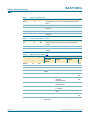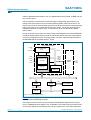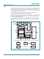
1
SAA7130HL
PCI video broadcast decoder
Rev. 04 — 11 April 2006
Product data sheet
1. General description
The SAA7130HL is a single chip solution to digitize and decode video, and capture it
through the PCI-bus.
Special means are incorporated to maintain the synchronization of audio to video. The
device offers versatile peripheral interfaces (GPIO) that support various extended
applications, e.g. analog audio pass-through for loopback cable to the sound card, or
capture of DTV and DVB transport streams, such as Vestigial Side Band (VSB),
Orthogonal Frequency Division Multiplexing (OFDM) and Quadrature Amplitude
Modulation (QAM) decoded digital television standards, see Figure 1.
I 2C-bus
TV TUNER:
CABLE
TERRESTRIAL
SATELLITE
IF-PLL:
DVB
ATV
DTV
DVB
DIGITAL CHANNEL DECODER:
VSB
QAM
OFDM
I 2C-BUS
EEPROM
SIF
AUDIO
DECODER:
BTSC
TS
CVBS
AF
(mono)
audio
L/R
CVBS
S-video
I 2S-bus
DECODER FOR TV VIDEO
WITH TS INTERFACE AND
DMA MASTER INTO PCI-BUS
audio I/O
line-in
line-out
ENCODER:
MPEG2
ITU656
SAA7130HL
mhc169
PCI-bus
Fig 1. Application diagram for capturing live TV video in the PC, with optional extensions for enhanced DTV and
DVB capture
1.1 Introduction
The PCI video broadcast decoder SAA7130HL is a highly integrated, low cost and solid
foundation for TV capture in the PC, for analog TV and digital video broadcast. The
various multimedia data types are transported over the PCI-bus by bus-master-write, to
optimally exploit the streaming capabilities of a modern host-based system. Legacy
requirements are also taken care of.
SAA7130HL
Philips Semiconductors
PCI video broadcast decoder
The SAA7130HL meets the requirements of PC design guides 98/99 and 2001 and is
PCI 2.2 and Advanced Configuration and Power Interface (ACPI) compliant.
The analog video is sampled by 9-bit ADCs, decoded by a multi-line adaptive comb filter
and scaled horizontally, vertically and by field rate. Multiple video output formats (YUV and
RGB) are available, including packed and planar, gamma-compensated or
black-stretched.
Audio is routed as an analog signal via the loopback cable to the sound card.
The SAA7130HL provides a versatile peripheral interface to support system extensions,
e.g. MPEG encoding for time-shift viewing, or DSP applications for audio enhancements.
The channel decoder for digital video broadcast reception (ATSC or DVB) can re-use the
integrated video ADCs.
The Transport Stream (TS) is collected by a tailored interface and pumped through the
PCI-bus to the system memory in well-defined buffer structures. Various internal events,
or peripheral status information, can be enabled as an interrupt on the PCI-bus.
1.2 Overview of TV decoders with PCI bridge
A TV decoder family with PCI interfacing has been created to support worldwide
TV broadcasting. The pin compatibility of these TV decoders offers the opportunity to
support different TV broadcast standards with one PCB layout.
Table 1:
TV decoder family with PCI interfacing
TV decoder type [1]
TV parameter
SAA7130HL SAA7133HL SAA7134HL SAA7135HL
PCI bridge
version
2.2
2.2
2.2
2.2
DMA channel
7
7
7
7
TV video
decoding
PAL, NTSC and
SECAM
X
X
X
X
Video
scaling
2 dimension and
2 task scaler
X
X
X
X
Raw VBI
27 MHz sampling rate
X
X
X
X
TV sound
decoding
FM A2 and NICAM
-
-
X
X
BTSC (dbx-TV) plus
SAP; EIAJ
-
X
-
X
stereo sampling
(I2S-bus and DMA)
-
32 kHz
32 kHz,
48 kHz
32 kHz,
48 kHz
FM radio stereo
-
X
-
X
Radio
SAA7130HL_4
Product data sheet
© Koninklijke Philips Electronics N.V. 2006. All rights reserved.
Rev. 04 — 11 April 2006
2 of 46
SAA7130HL
Philips Semiconductors
PCI video broadcast decoder
Table 1:
TV decoder family with PCI interfacing…continued
TV decoder type [1]
TV parameter
SAA7130HL SAA7133HL SAA7134HL SAA7135HL
Audio
left and right
pass-through
X
X
X
X
stereo sampling
(I2S-bus and DMA)
-
32 kHz,
44.1 kHz,
48 kHz
32 kHz,
44.1 kHz,
48 kHz
32 kHz,
44.1 kHz,
48 kHz
video frame locked
audio
-
X
X
X
incredible surround
-
X
X
X
volume, bass and
treble control
-
X
volume only
X
Transport
stream
serial and parallel TS
X
X
X
X
GPIO
static I/O pins
27
27
27
27
interrupt input pins
4
4
4
4
I2C-bus
X
X
X
X
X
X
X
X
multi-master
or slave
video out
[1]
X = function available.
1.3 Related documents
This document describes the functionality and characteristics of the SAA7130HL.
Other documents related to the SAA7130HL are:
• User manual SAA7130HL/34HL, describing the programmability
• Application note SAA7130HL/34HL, pointing out recommendations for system
implementation
• Demonstration and reference boards, including description, schematics, etc.:
– Proteus-Pro: TV capture PCI card for analog TV (standards: B/G, I, D/K and L/L’)
– Europe: hybrid DVB-T and analog TV capture PCI card for European broadcasting.
• Data sheets of other devices referred to in this document, e.g:
– TDA8961: DTV channel decoder
– TD1316: ATV+DVB-T tuner
– TDA10045: DVB channel receiver
– TDA9886: analog IF-PLL
– TDA9889: digital IF-PLL
SAA7130HL_4
Product data sheet
© Koninklijke Philips Electronics N.V. 2006. All rights reserved.
Rev. 04 — 11 April 2006
3 of 46
SAA7130HL
Philips Semiconductors
PCI video broadcast decoder
2. Features
2.1 PCI and DMA bus mastering
■
■
■
■
■
■
PCI 2.2 compliant including full Advanced Configuration and Power Interface (ACPI)
System vendor ID, etc. via EEPROM
Hardware support for virtual addressing by MMU
DMA bus master write for video, VBI and TS
Configurable PCI FIFOs, graceful overflow
Packed and planar video formats, overlay clipping
2.2 TV video decoder and video scaling
■
■
■
■
■
■
■
■
■
■
■
■
■
■
■
All-standards TV decoder: NTSC, PAL and SECAM
Five analog video inputs: CVBS and S-video
Video digitizing by two 9-bit ADCs at 27 MHz
Sampling according ITU-R BT.601 with 720 pixels/line
Adaptive comb filter for NTSC and PAL, also operating for non-standard signals
Automatic TV standard detection
Three level Macrovision copy protection detection according to Macrovision detect
specification revision 1
Control of brightness, contrast, saturation and hue
Versatile filter bandwidth selection
Horizontal and vertical downscaling or zoom
Adaptive anti-alias filtering
Capture of raw VBI samples
Two alternating settings for active video scaling
Output in YUV and RGB
Gamma compensation, black stretching
2.3 TV audio I/O
■ Integrated analog audio pass-through for analog audio loopback cable to sound card
2.4 Peripheral interface
■
■
■
■
■
I2C-bus master interface: 3.3 V and 5 V
Digital video output: ITU and VIP formats
TS input: serial or parallel
General purpose I/O, e.g. for strapping and interrupt
Propagate reset and ACPI state D3-hot
2.5 General
■
■
■
■
Package: LQFP128
Power supply: 3.3 V only
Power consumption of typical application: 1 W
Standby state (D3-hot): < 0.02 W
SAA7130HL_4
Product data sheet
© Koninklijke Philips Electronics N.V. 2006. All rights reserved.
Rev. 04 — 11 April 2006
4 of 46
SAA7130HL
Philips Semiconductors
PCI video broadcast decoder
■ All interface signals 5 V tolerant
■ Reference designs available
■ SDK for Windows (98, 2000 and XP) and Windows Driver Model (WDM)
3. Ordering information
Table 2:
Ordering information
Type
number
Package
Name
Description
Version
SAA7130HL
LQFP128
plastic low profile quad flat package; 128 leads;
body 14 × 20 × 1.4 mm
SOT425-1
4. Block diagram
baseband
audio
inputs
left 1
right 1
left 2
right 2
ANALOG
NF/AUDIO
FRONT-END
STEREO
BUFFER
audio
stereo
output
AUDIO
OUTPUT
CV2
CV3
CV4
TS data
digital TS data
data I 2S-bus
inputs
GPIO
ANALOG
VIDEO
FRONT-END
9-BIT
VIDEO
ADC
9-BIT
VIDEO
ADC
DIGITAL VIDEO
COMB FILTER
DECODER
VIDEO
SCALER
PIXEL ENGINE:
MATRIX
GAMMA
FORMAT
PCI INTERFACE
CV1
CVBS
S-video
inputs
ANALOG
VIDEO
FRONT-END
PCI-bus
REGISTER
UNIT
I 2C-bus
DMA
CV0
FIFO
SAA7130HL
TS PARALLEL
interrupt
TS SERIAL
STATIC I/O
IRQ
ITU656
mhc170
Fig 2. Block diagram
SAA7130HL_4
Product data sheet
© Koninklijke Philips Electronics N.V. 2006. All rights reserved.
Rev. 04 — 11 April 2006
5 of 46
SAA7130HL
Philips Semiconductors
PCI video broadcast decoder
5. Pinning information
5.1 Pinning
The SAA7130HL is packaged in a rectangular Low profile Quad Flat Package (LQFP) with
128 pins, see Figure 3.
All the pins are shown sorted by number in Table 3.
Functional pin groupings are given in the following tables:
Power supply pins: Table 4
PCI interface pins: Table 5
Analog interface pins: Table 6
Joint Test Action Group (JTAG) test interface pins for boundary scan test: Table 7
I2C-bus multi-master interface: Table 8
General purpose interface (pins GPIO) and the main functions: Table 9
103
128
The characteristics of the pin types are detailed in Table 10.
102
1
SAA7130HL
64
65
39
38
001aac204
Fig 3. Pin configuration
Table 3:
Pin allocation table
Pin
Symbol
Pin
Symbol
Pin
Symbol
Pin
Symbol
1
VDDD
33
C/BE[1]#
65
VDDD
97
VSSA
2
GNT#
34
AD[15]
66
V_CLK
98
RIGHT1
3
REQ#
35
AD[14]
67
GPIO17
99
VREF0
4
AD[31]
36
AD[13]
68
GPIO16
100 RIGHT2
5
AD[30]
37
AD[12]
69
GPIO15
101 n.c.
6
AD[29]
38
VDDD
70
GPIO14
102 n.c.
7
AD[28]
39
VSSD
71
GPIO13
103 OUT_RIGHT
8
AD[27]
40
PCI_CLK
72
GPIO12
104 OUT_LEFT
9
AD[26]
41
AD[11]
73
VDDD
105 PROP_RST_N
SAA7130HL_4
Product data sheet
© Koninklijke Philips Electronics N.V. 2006. All rights reserved.
Rev. 04 — 11 April 2006
6 of 46
SAA7130HL
Philips Semiconductors
PCI video broadcast decoder
Table 3:
Pin allocation table…continued
Pin
Symbol
Pin
Symbol
Pin
Symbol
Pin
10
AD[25]
42
AD[10]
74
VSSD
106 n.c.
Symbol
11
AD[24]
43
AD[09]
75
GPIO11
107 VREF3
12
C/BE[3]#
44
AD[08]
76
GPIO10
108 VSSA
13
IDSEL
45
C/BE[0]#
77
GPIO9
109 CV2_C
14
AD[23]
46
AD[07]
78
GPIO8
110 VDDA
15
AD[22]
47
AD[06]
79
GPIO7
111 n.c.
16
AD[21]
48
AD[05]
80
GPIO6
112 DRCV_Y
17
AD[20]
49
AD[04]
81
GPIO5
113 VSSA
18
AD[19]
50
AD[03]
82
GPIO4
114 CV0_Y
19
VDDD
51
AD[02]
83
GPIO3
115 VDDA
20
VSSD
52
AD[01]
84
GPIO2
116 CV1_Y
21
AD[18]
53
AD[00]
85
GPIO1
117 DRCV_C
22
AD[17]
54
VDDD
86
GPIO0
118 CV3_C
23
AD[16]
55
VSSD
87
GPIO27
119 VSSA
24
C/BE[2]#
56
GPIO23
88
GPIO26
120 CV4
25
FRAME#
57
GPIO22
89
GPIO25
121 TRST_N
26
IRDY#
58
GPIO21
90
SCL
122 TCK
27
TRDY#
59
GPIO20
91
SDA
123 TMS
28
DEVSEL#
60
GPIO19
92
VDDD
124 TDO
29
STOP#
61
GPIO18
93
VSSD
125 TDI
30
PERR#
62
XTALI
94
LEFT2
126 INT_A
31
SERR#
63
XTALO
95
VDDA
127 PCI_RST#
32
PAR
64
VSSD
96
LEFT1
128 VSSD
5.2 Pin description
Table 4:
Power supply pins
Symbol
Pin
Type
Description
VSSA
97, 108,
113
and 119
AG
analog ground for integrated analog signal processing
VDDA
95, 110
and 115
AS
analog supply voltage for integrated analog signal
processing
VSSD
20, 39, 55,
64, 74, 93
and 128
VG
digital ground for digital circuit, core and input/outputs
VDDD
1, 19, 38,
54, 65, 73
and 92
VS
digital supply voltage for digital circuit, core and
input/outputs
SAA7130HL_4
Product data sheet
© Koninklijke Philips Electronics N.V. 2006. All rights reserved.
Rev. 04 — 11 April 2006
7 of 46
SAA7130HL
Philips Semiconductors
PCI video broadcast decoder
Table 5:
PCI interface pins
[1]
Symbol
Pin
Type
Description
PCI_CLK
40
PI
PCI clock input: reference for all bus transactions, up to
33.33 MHz
PCI_RST#
127
PI
PCI reset input: will 3-state all PCI pins (active LOW)
AD[31] to
AD[00]
4 to 11,
14 to 18,
21 to 23,
34 to 37,
41 to 44
and
46 to 53
PIO and
T/S
multiplexed address and data input or output:
bidirectional, 3-state
C/BE[3]# to
C/BE[0]#
12, 24, 33 PIO and
and 45
T/S
command code input or output: indicates type of
requested transaction and byte enable, for byte aligned
transactions (active LOW)
PAR
32
PIO and
T/S
parity input or output: driven by the data source, even
parity over all pins AD and C/BE#
FRAME#
25
PIO and
S/T/S
frame input or output: driven by the current bus master
(owner), to indicate the beginning and duration of a bus
transaction (active LOW)
TRDY#
27
PIO and
S/T/S
target ready input or output: driven by the addressed
target, to indicate readiness for requested transaction
(active LOW)
IRDY#
26
PIO and
S/T/S
initiator ready input or output: driven by the initiator, to
indicate readiness to continue transaction (active LOW)
STOP#
29
PIO and
S/T/S
stop input or output: target is requesting the master to
stop the current transaction (active LOW)
IDSEL
13
PI
initialization device select input: this input is used to
select the SAA7130HL during configuration read and
write transactions
DEVSEL#
28
PIO and
S/T/S
device select input or output: driven by the target device,
to acknowledge address decoding (active LOW)
REQ#
3
PO
PCI request output: the SAA7130HL requests master
access to PCI-bus (active LOW)
GNT#
2
PI
PCI grant input: the SAA7130HL is granted to master
access PCI-bus (active LOW)
INT_A
126
PO and
O/D
interrupt A output: this pin is an open-drain interrupt
output, conditions assigned by the interrupt register
PERR#
30
PIO and
S/T/S
parity error input or output: the receiving device detects
data parity error (active LOW)
SERR#
31
PO and
O/D
system error output: reports address parity error (active
LOW)
[1]
PCI-bus pins are located on the long side of the package to simplify PCI board layout requirements.
Table 6:
Analog interface pins
[1]
Symbol
Pin
Type
Description
XTALI
62
CI
quartz oscillator input: 32.11 MHz or 24.576 MHz
XTALO
63
CO
quartz oscillator output
LEFT2
94
AI
analog audio stereo left 2 input or mono input
SAA7130HL_4
Product data sheet
© Koninklijke Philips Electronics N.V. 2006. All rights reserved.
Rev. 04 — 11 April 2006
8 of 46
SAA7130HL
Philips Semiconductors
PCI video broadcast decoder
Table 6:
Analog interface pins…continued [1]
Symbol
Pin
Type
Description
VDDA
95
AS
analog supply voltage (3.3 V)
LEFT1
96
AI
analog audio stereo left 1 input or mono input; default
analog pass-through to pin OUT_LEFT after reset
VSSA
97
AG
analog ground (for audio)
RIGHT1
98
AI
analog audio stereo right 1 input or mono input; default
analog pass-through to pin OUT_RIGHT after reset
VREF0
99
AR
analog reference ground for audio Sigma Delta ADC; to be
connected directly to analog ground (VSSA)
RIGHT2
100
AI
analog audio stereo right 2 input or mono input
n.c.
101
-
not connected
n.c.
102
-
not connected
OUT_RIGHT
103
AO
analog audio stereo right channel output; 1 V (RMS)
line-out, feeding the audio loopback cable via a coupling
capacitor of 2.2 µF
OUT_LEFT
104
AO
analog audio stereo left channel output; 1 V (RMS) line-out,
feeding the audio loopback cable via a coupling capacitor of
2.2 µF
PROP_RST_N
105
AO
analog output for test and debug purposes (active LOW)
n.c.
106
-
not connected
VREF3
107
AR
analog reference voltage for audio FIR-DAC and SCART
audio input buffer; to be supported with two parallel
capacitors of 47 µF and 0.1 µF to analog ground (VSSA)
VSSA
108
AG
analog ground
CV2_C
109
AI
composite video input (mode 2) or C input (modes 6 and 8)
VDDA
110
AS
analog power supply (3.3 V)
n.c.
111
-
not connected
DRCV_Y
112
AR
differential reference connection (for CV0 and CV1); to be
supported with a capacitor of 47 nF to analog ground (VSSA)
VSSA
113
AG
analog ground
CV0_Y
114
AI
composite video input (mode 0) or Y input (modes 6 and 8)
VDDA
115
AS
analog supply voltage (3.3 V)
CV1_Y
116
AI
composite video input (mode 1) or Y input (modes 7 and 9)
DRCV_C
117
AR
differential reference connection (for CV2, CV3 and CV4); to
be supported with a capacitor of 47 nF to analog ground
(VSSA)
CV3_C
118
AI
composite video input (mode 3) or C input (modes 7 and 9)
VSSA
119
AG
analog ground
CV4
120
AI
composite video input (mode 4)
[1]
The SAA7130HL offers an interface for analog video and audio signals. The related analog supply pins are
included in this table.
SAA7130HL_4
Product data sheet
© Koninklijke Philips Electronics N.V. 2006. All rights reserved.
Rev. 04 — 11 April 2006
9 of 46
SAA7130HL
Philips Semiconductors
PCI video broadcast decoder
Table 7:
JTAG test interface pins
Symbol
Pin
Type
Description
TRST_N
121
I
test reset input: drive LOW for normal operating (active
LOW)
TCK
122
I
test clock input: drive LOW for normal operating
TMS
123
I
test mode select input: tie HIGH or let float for normal
operating
TDO
124
O
test serial data output: 3-state
TDI
125
I
test serial data input: tie HIGH or let float for normal
operating
Table 8:
I2C-bus multi-master interface
Symbol
Pin
Type
Description
SCL
90
IO2
serial clock input (slave mode) or output (multi-master
mode)
SDA
91
IO2
serial data input and output; always available
PROP_RST_N
105
GO
propagate reset and D3-hot output; to peripheral board
circuitry
Table 9:
Symbol
GPIO pins and functions
Pin
Type
[1]
Function
Audio and
video port
outputs
TS capture
inputs
Raw DTV/DVB
outputs
GPIO
GPIO27
87
GIO
-
-
-
R/W
GPIO26
88
GIO
-
-
-
R/W
GPIO25
89
GIO
-
-
-
R/W
V_CLK
66
GO
V_CLK (also
gated)
-
ADC_CLK (out)
-
GPIO23
56
GIO
HSYNC
-
ADC_C[0] (LSB)
R/W,
INT
GPIO22
57
GIO
VSYNC
TS_LOCK
(channel
decoder locked)
-
R/W,
INT
GPIO21
58
GIO
-
TS_S_D
(bit-serial data)
-
R/W
GPIO20
59
GIO
-
TS_CLK
(< 33 MHz)
-
R/W
GPIO19
60
GIO
-
TS_SOP (packet start)
R/W
GPIO18
61
GIO
VAUX2
-
X_CLK_IN
R/W,
INT
GPIO17
67
GIO
VAUX1 (e.g.
VACTIVE)
-
ADC_Y[0] (LSB)
R/W
SAA7130HL_4
Product data sheet
© Koninklijke Philips Electronics N.V. 2006. All rights reserved.
Rev. 04 — 11 April 2006
10 of 46
SAA7130HL
Philips Semiconductors
PCI video broadcast decoder
Table 9:
Symbol
GPIO pins and functions…continued [1]
Pin
Type
Audio and
video port
outputs
TS capture
inputs
Raw DTV/DVB
outputs
GPIO
-
TS_VAL (valid
flag)
-
R/W,
INT
GPIO16
68
GPIO15 to
GPIO8
69 to 72 GIO
and
75 to 78
VP[7:0] for
formats:
ITU-R BT.656,
VMI, VIP (1.1,
2.0), etc.
-
ADC_Y[8:1]
R/W
GPIO7 to
GPIO0
79 to 86 GIO
VP extension
for 16-bit
formats: ZV,
VIP-2, DMSD,
etc.
TS_P_D[7:0]
(byte-parallel
data)
ADC_C[8:1]
R/W
[1]
GIO
Function
The SAA7130HL offers a peripheral interface with General Purpose Input/Output (GPIO) pins. Dedicated
functions can be selected:
a) Digital Video Port (VP): output only; in 8-bit and 16-bit formats, such as VMI, DMSD (ITU-R BT.601);
zoom-video, with discrete sync signals; ITU-R BT.656; VIP (1.1 and 2.0), with sync encoded in SAV and
EAV codes.
b) Transport Stream (TS) capture input: from the peripheral DTV/DVB channel decoder; synchronized by
Start Of Packet (SOP); in byte-parallel or bit-serial protocol.
c) Digitized raw DTV/DVB samples stream output: from internal ADCs; to feed the peripheral DTV/DVB
channel decoder.
d) GPIO: as default (no other function selected); static (no clock); read and write from or to individually
selectable pins; latching ‘strap’ information at system reset time.
e) Use an external pull-up resistor of 4.7 kΩ at GPIO16 for an external 24.576 MHz crystal; due to an
internal pull-down resistor an open GPIO16 pin requires an external 32.11 MHz crystal.
f) Peripheral interrupt (INT) input: enabled by interrupt enable register; routed to PCI interrupt (INT_A).
5.2.1 Pin type description
Table 10:
Characteristics of pin types and remarks
Pin type
Description
AG
analog ground
AI
analog input; video, audio and sound
AO
analog output
AR
analog reference support pin
AS
analog supply voltage (3.3 V)
CI
CMOS input; 3.3 V level (not 5 V tolerant)
CO
CMOS output; 3.3 V level (not 5 V tolerant)
GIO
digital input/output (GPIO); 3.3 V level (5 V tolerant)
GO
digital output (GPIO); 3.3 V level (5 V tolerant)
I
JTAG test input
IO2
digital input and output of the I2C-bus interface; 3.3 V and 5 V
compatible, auto-adapting
O
JTAG test output
O/D
open-drain output (for PCI-bus); multiple clients can drive LOW at the
same time, wired-OR, floating back to 3-state over several clock cycles
SAA7130HL_4
Product data sheet
© Koninklijke Philips Electronics N.V. 2006. All rights reserved.
Rev. 04 — 11 April 2006
11 of 46
SAA7130HL
Philips Semiconductors
PCI video broadcast decoder
Table 10:
Characteristics of pin types and remarks…continued
Pin type
Description
PI
input according to PCI-bus requirements
PIO
input and output according to PCI-bus requirements
PO
output according to PCI-bus requirements
S/T/S
sustained 3-state (for PCI-bus); previous owner drives HIGH for one
clock cycle before leaving to 3-state
T/S
3-state I/O (for PCI-bus); bidirectional
VG
ground for digital supply
VS
supply voltage (3.3 V)
Name ends with _N or # this pin or ‘signal’ is active LOW, i.e. the function is ‘true’ if the logic level
is LOW
6. Functional description
6.1 Overview of internal functions
The SAA7130HL is able to capture TV signals over the PCI-bus in personal computers by
a single chip; see Figure 4.
The SAA7130HL incorporates two 9-bit video ADCs and the entire decoding circuitry for
any analog TV signal: NTSC, PAL and SECAM, including non-standard signals, such as
playback from a VCR. The adaptive multi-line comb filter provides superb picture quality,
component separation, sharpness and high bandwidth. The video stream can be cropped
and scaled to the needs of the application. Scaling down as well as zooming up is
supported in the horizontal and vertical direction, and an adaptive filter algorithm prevents
aliasing artifacts. With the acquisition unit of the scaler two different ‘tasks’ can be defined,
e.g. to capture video to the CPU for compression, and write video to the screen from the
same video source but with different resolution, color format and frame rate.
The SAA7130HL incorporates analog audio pass-through and support for the analog
audio loopback cable to the sound card function.
The decoded video streams are fed to the PCI-bus, and are also applied to a peripheral
streaming interface, in ITU, VIP or VMI format. A possible application extension is
on-board hardware MPEG compression, or other feature processing. The compressed
data is fed back through the peripheral interface, in parallel or serial format, to be captured
by the system memory through the PCI-bus. The Transport Stream (TS) from a DTV/DVB
channel decoder can be captured through the peripheral interface in the same way.
Video and transport streams are collected in a configurable FIFO with a total capacity of
1 kB. The DMA controller monitors the FIFO filling degree and master-writes the audio
and video stream to the associated DMA channel. The virtual memory address space
(from OS) is translated into physical (bus) addresses by the on-chip hardware Memory
Management Unit (MMU).
The application of the SAA7130HL is supported by reference designs and a set of drivers
for the Windows operating system (Windows driver model compliant).
SAA7130HL_4
Product data sheet
© Koninklijke Philips Electronics N.V. 2006. All rights reserved.
Rev. 04 — 11 April 2006
12 of 46
SAA7130HL
Philips Semiconductors
PCI video broadcast decoder
GPIO
5 analog
video
inputs
INPUT SELECTION
CLAMP AND GAIN
CONTROL
digital video
output
I 2C-bus
VIDEO PORT
(DIGITAL)
I 2C-BUS
INTERFACE
reset
transport
stream input
stereo
output
stereo
input 1
stereo
input 2
DTV-TS p/s
ANALOG AUDIO I/O
I 2S-BUS
INPUT
PASS-THROUGH (DEFAULT)
9-BIT ADC 9-BIT ADC
DECODER
(NTSC, PAL, SECAM)
PROPAGATE
RESET
LLC
ADAPTIVE
COMB FILTER
SAA7130HL
VIDEO SCALER
MATRIX
3-D
GAMMA
RAW VBI
FORMAT
PROGRAM PROGRAM
SET
SET
VIDEO FIFOS
TS FIFOS
DMA CONTROL
DMA CONTROL
PCI-BUS INTERFACE
PCI-bus
BOUNDARY
SCAN TEST
OSCILLATOR
ACPI POWER
MANAGEMENT
test
crystal
mhc171
Fig 4. Functional diagram
6.2 Application examples
The SAA7130HL enables PC TV capture applications both on the PC motherboard and
on PCI add-on TV capture cards. Figure 5 and Figure 6 illustrate some examples of
add-on card applications.
Figure 5 shows the basic application to capture video from analog TV sources. The
proposed tuner types incorporate the RF tuning function and the IF down conversion.
Usually the IF down conversion stage also includes a single channel and analog sound
FM demodulator. The Philips tuner FI1216 MK2 is dedicated to the 50 Hz system
B/G standard as used in Europe. The FI1236 MK2 is the comparable type for the 60 Hz
system M standard for the USA. Both types are suited for terrestrial broadcast and for
cable reception. The tuner provides composite video and baseband audio as mono or
‘multiplexed’ (mpx) in case of BTSC. These analog video and sound signals are fed to the
appropriate input pins of the SAA7130HL.
Further analog video input signals, CVBS and/or Y-C, can be connected via the board
back panel, or the separate front connectors, e.g. from a camcorder. Accompanying
stereo audio signals can also be fed to the SAA7130HL.
SAA7130HL_4
Product data sheet
© Koninklijke Philips Electronics N.V. 2006. All rights reserved.
Rev. 04 — 11 April 2006
13 of 46
SAA7130HL
Philips Semiconductors
PCI video broadcast decoder
Video is digitized and decoded to YUV. The digital streams are pumped via DMA into the
PCI memory space.
The SAA7130HL incorporates the means for legacy analog audio signal routing. The
analog audio input signal is fed via an analog audio loopback cable into the line-in of a
legacy sound card. An external audio signal, that would have otherwise connected directly
to the sound card, is now routed through the SAA7130HL. This analog pass-through is
enabled as default by a system reset, i.e. without any driver involvement and before
system setup.
During the power-up procedure, the SAA7130HL will investigate the on-board EEPROM
to load the board-specific system vendor ID and board version ID into the related places
of the PCI configuration space. The board vendor can store other board-specific data in
the EEPROM that is accessible via the I2C-bus.
TV CAPTURE PCI CARD
TV cable
or
terrestrial
TV TUNER AND
IF-PLL
I 2C-bus
CVBS
AF sound
(mono)
analog
audio
loopback
cable
CVBS
S-video
DECODER FOR
TV VIDEO
audio
line-in
DMA MASTER
INTO PCI
SOUND
CARD
I 2C-BUS EEPROM
SYSTEM
VENDOR ID
SAA7130HL
PCI-bus:
digital video, raw VBI, TS
SOUTH
BRIDGE
NORTH
BRIDGE
AGP
VGA AND
LOCAL MEMORY
ISA
SYSTEM
MEMORY
FSB
CPU AND
CACHE MEMORY
mhc172
Fig 5. TV mono capture card
Figure 6 shows an application extension with a hybrid TV tuner front-end and digital
terrestrial channel decoding for DVB-T.
The single-conversion tuner TD1316 provides two dedicated IF signals for the analog
IF-PLL (TDA9886) and the digital IF-PLL (TDA9889). The CVBS (video) and AUD (audio,
mono) output signals of the analog IF-PLL can be routed to one of the video inputs and
SAA7130HL_4
Product data sheet
© Koninklijke Philips Electronics N.V. 2006. All rights reserved.
Rev. 04 — 11 April 2006
14 of 46
SAA7130HL
Philips Semiconductors
PCI video broadcast decoder
the audio (left or right) input of the SAA7130HL for analog video decoding and direct audio
streaming to the sound card. On the other hand, the 2nd IF signal of the digital IF-PLL is
fed directly to the interface of the channel decoder (TDA10045), which decodes the signal
into a digital DVB-T Transport Stream (TS).
The SAA7130HL captures this TS via the dedicated peripheral interface into the
configurable internal FIFO for DMA into the PCI memory space.
The packet structure as decoded by the TDA10045 is maintained in a well-defined buffer
structure in the system memory, and therefore can easily be sorted (de-multiplexed) by
the CPU for proper MPEG decoding.
The Broadcast Driver Architecture (BDA) for Windows operating systems supports this
type of hybrid TV capture application, sharing one capture board for analog and digital
TV reception.
HYBRID TV CAPTURE PCI CARD
ATV cable
or terrestrial
and
DVB terrestrial
IF
TV TUNER
DIGITAL
IF-PLL
IF
DVB-T
CHANNEL
DECODER
ANALOG IF-PLL
AF
CVBS
TS
CVBS
S-video
analog audio
loopback
cable
DECODER FOR
TV VIDEO
audio
I 2C-bus
line-in
DMA MASTER
INTO PCI
SOUND
CARD
I 2C-BUS EEPROM
SYSTEM
VENDOR ID
SAA7130HL
PCI-bus:
digital video, raw VBI, TS
SOUTH
BRIDGE
NORTH
BRIDGE
AGP
VGA AND
LOCAL MEMORY
ISA
SYSTEM
MEMORY
FSB
CPU AND
CACHE MEMORY
mhc173
Fig 6. Hybrid TV capture board for digital TV (DVB-T) and analog TV reception
SAA7130HL_4
Product data sheet
© Koninklijke Philips Electronics N.V. 2006. All rights reserved.
Rev. 04 — 11 April 2006
15 of 46
SAA7130HL
Philips Semiconductors
PCI video broadcast decoder
6.3 Software support
6.3.1 Device driver
A complex and powerful software packet is provided for the SAA7130HL. This packet
includes plug-and-play driver and capture driver installations for all commonly used 32-bit
Windows platforms.
All platform related drivers support the following:
• Video preview and capture interfaces
Table 11:
Microsoft Operation System (MOS) support
MOS
Driver support
Windows 98
Device access is contained in a kernel-mode Windows Driver Model (WDM)
driver. The capture driver interface is based on Microsoft DirectShow technology.
Windows 2000 The driver is binary-compatible with the Windows 98 driver and validated for
passing the Microsoft WHQL test for getting the Win2000 driver signature.
Windows XP
The driver is binary-compatible with the Windows 98 driver and validated for
passing the Microsoft WHQL test for getting the WinXP driver signature.
6.3.2 Supporting WDM
The Windows driver is implemented as an AV-streaming class-driver and provides a
‘DirectShow’ (DS) filter with output pins for video preview, video capture and VBI, together
with a crossbar for input sources selection.
The TV tuner filter is a separate child driver and supports the control of all common Philips
CAN and Silicon tuners. The typical filter structure is shown in Figure 7.
TV TUNER
XBAR
SAA7130HL
external video inputs
audio inputs
CAPTURE
DRIVER
video preview
video capture
VBI
transport stream in
mhc174
Fig 7. WDM capture driver filters
6.4 PCI interface
6.4.1 PCI configuration registers
The PCI interface of the SAA7130HL complies with the PCI specification 2.2 and supports
power management and Advanced Configuration and Power Interface (ACPI) as required
by the PC Design Guide 2001.
The PCI specification defines a structure of the PCI configuration space that is
investigated during the boot-up of the system. The configuration registers (see Table 12)
hold information essential for plug-and-play, to allow system enumeration and basic
SAA7130HL_4
Product data sheet
© Koninklijke Philips Electronics N.V. 2006. All rights reserved.
Rev. 04 — 11 April 2006
16 of 46
SAA7130HL
Philips Semiconductors
PCI video broadcast decoder
device setup without depending on the device driver, and support association of the
proper software driver. Some of the configuration information is hard-wired in the device;
some information is loaded during the system start-up.
Table 12:
PCI configuration registers
Function
Register address Value
(hexadecimal)
Device vendor ID
00 and 01
[1]
Remark
1131h
for Philips
Device ID
02 and 03
7130h
for SAA7130HL
Revision ID
08
00h
or higher
Class code
09 to 0B
04 8000h
multimedia
Memory address
space required
10 to 13
XXXX XXXX XXXX XXXX
XXXX XX00 0000 0000b
1 kB
System (board)
vendor ID
2C and 2D
loaded from EEPROM
Sub-system (board
version) ID
2E and 2F
loaded from EEPROM
[1]
X = don’t care.
The device vendor ID is hard coded to 1131h, which is the code for Philips as registered
with PCI-SIG.
The device ID is hard coded to 7130h.
During power-up, initiated by PCI reset, the SAA7130HL fetches additional system
information via the I2C-bus from the on-board EEPROM, to load actual board-type specific
codes for the system vendor ID, sub-system ID (board version) and ACPI related
parameters into the configuration registers.
6.4.2 ACPI and power states
The PCI specification 2.2 requires support of Advanced Configuration and Power
Interface specification 1.0 (ACPI); more details are defined in the PCI Power Management
Specification 1.0.
The power management capabilities and power states are reported in the extended
configuration space. The main purpose of ACPI and PCI power management is to tailor
the power consumption of the device to the actual needs.
The SAA7130HL supports all four ACPI device power states (see Table 13).
The pin PROP_RST_N of the peripheral interface is switched active LOW during the PCI
reset procedure, and for the duration of the D3-hot state. Peripheral devices on board of
the add-on card should use the level of this signal PROP_RST_N to switch themselves in
any Power-save mode (e.g. disable device) and reset to default settings on the rising edge
of signal PROP_RST_N.
SAA7130HL_4
Product data sheet
© Koninklijke Philips Electronics N.V. 2006. All rights reserved.
Rev. 04 — 11 April 2006
17 of 46
SAA7130HL
Philips Semiconductors
PCI video broadcast decoder
Table 13:
Power management table
Power state
Description
D0
Normal operation: all functions accessible and programmable. The default setting
after reset and before driver interaction (D0 un-initialized) switches most of the
circuitry of the SAA7130HL into the Power-down mode, effectively such as
D3-hot.
D1
First step of reduced power consumption: no functional operation. Program
registers are not accessible, but content is maintained. Most of the circuitry of the
SAA7130HL is disabled with exception of the crystal and real-time clock
oscillators, so that a quick recovery from D1 to D0 is possible.
D2
Second step of reduced power consumption: no functional operation. Program
registers are not accessible, but content is maintained. All functional circuitry of
the SAA7130HL is disabled, including the crystal and clock oscillators.
D3-hot
Lowest power consumption: no functional operation. The content of the
programming registers gets lost and is set to default values when returning to D0.
6.4.3 DMA and configurable FIFO
The SAA7130HL supports seven DMA channels to master-write captured active video,
raw VBI and DTV/DVB Transport Streams (TS) into the PCI memory. Each DMA channel
contains inherently the definition of two buffers, e.g. for odd and even fields in case of
interlaced video.
The DMA channels share in time and space one common FIFO pool of 256 Dwords
(1024 bytes) total. It is freely configurable how much FIFO capacity can be associated
with which DMA channel. Furthermore, a preferred minimum burst length can be
programmed, i.e. the amount of data to be collected before the request for the PCI-bus is
issued. This means that latency behavior per DMA channel can be tailored and optimized
for a given application.
In the event that a FIFO of a certain channel overflows due to latency conflict on the bus,
graceful overflow recovery is applied. The amount of data that gets lost because it could
not be transmitted, is monitored (counted) and the PCI-bus address pointer is
incremented accordingly. Thus new data will be written to the correct memory place, after
the latency conflict is resolved.
6.4.4 Virtual and physical addressing
Most operating systems allocate memory to requesting applications for DMA as
continuous ranges in virtual address space. The data flow over the PCI-bus points to
physical addresses, usually not continuous and split in pages of 4 kB (Intel architecture,
most UNIX systems, Power PC).
The association between the virtual (logic) address space and the fragmented physical
address space is defined in page tables (system files); see Figure 8.
The SAA7130HL incorporates hardware support (MMU) to translate virtual to physical
addresses on the fly, by investigating the related page table information. This hardware
support reduces the demand for real-time software interaction and interrupt requests, and
therefore saves system resources.
SAA7130HL_4
Product data sheet
© Koninklijke Philips Electronics N.V. 2006. All rights reserved.
Rev. 04 — 11 April 2006
18 of 46
SAA7130HL
Philips Semiconductors
PCI video broadcast decoder
physical memory
real-time streams
00000h
FIFO
POOL
00007h
DMA DEFINITIONS
(VIRTUAL ADDRESS SPACE)
page table
000h
0000Fh
007h
00001000h
00008000h
00009000h
0000A000h
0000D000h
00011000h
00014000h
00016000h
0001E000h
DMA
ADDRESS
GENERATION
VIRTUAL
TO
PHYSICAL
ADDRESS
TRANSLATION
00017h
PCI
TRANSFER AND
CONTROL
015h
0001Fh
physical address
space on PCI
= allocated memory space
= page table
mhb996
Fig 8. MMU implementation (shown bit width indication is valid for 4 kB mode)
6.4.5 Status and interrupts on PCI-bus
The SAA7130HL provides a set of status information about internal signal processing,
video standard detection, peripheral inputs and outputs (pins GPIO) and behavior on the
PCI-bus. This status information can be conditionally enabled to raise an interrupt on the
PCI-bus, e.g. completion of a certain DMA channel or buffer, or change in a detected
TV standard, or the state of peripheral devices.
The cause of an issued interrupt is reported in a dedicated register, even if the original
condition has changed before the system was able to investigate the interrupt.
6.5 Analog TV standards
Analog TV signals are described in three categories of standards:
• Basic TV systems: defining frame rate, number of lines per field, levels of
synchronization signals, blanking, black and white, signal bandwidth and the
RF modulation scheme
• Color transmission: defining color coding and modulation method
• Sound and stereo: defining coding for transmission
TV signals that are broadcast usually conform fairly accurately to the standards.
Transmission over the air or through a cable can distort the signal with noise, echoes,
crosstalk or other disturbances.
SAA7130HL_4
Product data sheet
© Koninklijke Philips Electronics N.V. 2006. All rights reserved.
Rev. 04 — 11 April 2006
19 of 46
SAA7130HL
Philips Semiconductors
PCI video broadcast decoder
Video signals from local consumer equipment, e.g. VCR, camcorder, camera, game
console, or even DVD player, often do not follow the standard specification very
accurately.
Playback from video tape cannot be expected to maintain correct timing, especially not
during feature mode (fast forward, etc.).
Table 14 to Table 16 list some characteristics of the various TV standards.
The SAA7130HL decodes all color TV standards and non-standard signals as generated
by video tape recorders e.g. automatic video standard detection can be applied, with
preference options for certain standards, or the decoder can be forced to a dedicated
standard.
Table 14:
Overview of basic TV standards
Main
parameters
Standard
M
N
B
G, H
I
D/K
L
RF channel
width
6
6
7
7
8
7
8
MHz
Video
bandwidth
4.2
4.2
5
5
5.5
6
6
MHz
1st sound
carrier
4.5 FM
4.5 FM
5.5 FM
5.5 FM
6.0 FM
6.5 FM
6.5 AM
MHz
Field rate
59.94006
50
50
50
50
50
50
Hz
Lines per frame 525
625
625
625
625
625
625
Line frequency
15.734
15.625
15.625
15.625
15.625
15.625
15.625
ITU clocks per
line
1716
1728
1728
1728
1728
1728
1728
Sync, setup
level
−40, 7.5
−40, 7.5
−43, 0
−43, 0
−43, 0
−43, 0
−43, 0
Gamma
correction
2.2
2.2
2.8
2.8
2.8
2.8
2.8
Associated
color
TV standards
NTSC, PAL
PAL
PAL
PAL
PAL
SECAM,
PAL
SECAM
Associated
stereo
TV sound
systems
BTSC, EIAJ, BTSC
A2
dual FM,
A2
NICAM
NICAM
NICAM, A2 NICAM
Country
examples
USA, Japan, Argentina
Brazil
part of
Europe,
Australia
Spain,
Malaysia,
Singapore
UK,
Northern
Europe
China,
Eastern
Europe
Table 15:
Unit
kHz
IRE
France,
Eastern
Europe
TV system color standards
Main
parameters
NTSC M
PAL M
PAL N
PAL BGHID SECAM LDGHK
PAL 4.4 (60 Hz) Unit
Field rate
59.94
59.94
50
50
50
≈60
Lines per
frame
525
525
625
625
625
525
Chrominance
subcarrier
3.580
3.576
3.582
4.434
4.406
SAA7130HL_4
Product data sheet
4.250
4.434
Hz
MHz
© Koninklijke Philips Electronics N.V. 2006. All rights reserved.
Rev. 04 — 11 April 2006
20 of 46
SAA7130HL
Philips Semiconductors
PCI video broadcast decoder
Table 15:
TV system color standards…continued
Main
parameters
NTSC M
PAL M
PAL N
PAL BGHID SECAM LDGHK
PAL 4.4 (60 Hz) Unit
fsc to H ratio
227.5
227.25
229.25
283.75
282
272
n.a.
fsc offset (PAL) -
-
50
50
-
-
n.a.
Alternating
phase
no
yes
yes
yes
-
-
yes
Country
examples
USA, Japan,
Asia-Pacific
Brazil
Middle and Europe,
South
CommonAmerica
wealth,
China
Table 16:
France,
Eastern Europe,
Africa, Middle East
Hz
VCR
transcoding
NTSC-tape to
PAL
TV stereo sound standards
Main parameters
Analog systems
Digital coding
Mono
BTSC
Stereo coding
scheme
-
internal carrier (mpx)
EIAJ
2-Carrier Systems (2CS)
AM
FM
2nd FM carrier
2nd language
-
mono SAP on
internal FM
as alternative
to stereo
as alternative to stereo mono on 1st carrier
Sound IF
A2 (dual FM)
Unit
NICAM
DQPSK on FM
1st
2nd
1st
2nd
M, N
4.5 FM
4.5
4.5
4.5
4.724
not used
not used
MHz
B, G, H
5.5 FM
not used
not used
5.5
5.742
5.5
5.850
MHz
I
6.0 FM
not used
not used
not used
not used
6.0
6.552
MHz
DK (1)
6.5 FM
not used
not used
6.5
6.742
6.5
5.850
MHz
DK (2)
6.5 FM
-
-
-
6.258
-
-
MHz
DK (3)
6.5 FM
-
-
-
5.742
-
-
MHz
L
6.5 AM
not used
not used
not used
not used
6.5
5.850
De-emphasis
75
75 dbx-TV
50
50 or 75
50 or J17
µs
Audio bandwidth
15
15
15
15
15
kHz
Country examples
worldwide
USA, South
America
Japan
part of Europe, Korea
part of Europe, China
MHz
6.6 Video processing
6.6.1 Analog video inputs
The SAA7130HL provides five analog video input pins:
• Composite video signals (CVBS), from tuner or external source
• S-video signals (pairs of Y-C), e.g. from camcorder
• DTV/DVB ‘low-IF’ signal, from an appropriate DTV or combi-tuner
Analog anti-alias filters are integrated on chip and therefore, no external filters are
required. The device also contains automatic clamp and gain control for the video input
signals, to ensure optimum utilization of the ADC conversion range. The nominal video
signal amplitude is 1 V (p-p) and the gain control can adapt deviating signal levels in the
range of +3 dB to −6 dB. The video inputs are digitized by two ADCs of 9-bit resolution,
with a sampling rate of nominal 27 MHz (the line-locked clock) for analog video signals.
SAA7130HL_4
Product data sheet
© Koninklijke Philips Electronics N.V. 2006. All rights reserved.
Rev. 04 — 11 April 2006
21 of 46
SAA7130HL
Philips Semiconductors
PCI video broadcast decoder
6.6.2 Video synchronization and line-locked clock
The SAA7130HL recovers horizontal and vertical synchronization signals from the
selected video input signal, even under extremely adverse conditions and signal
distortions. Such distortions are ‘noise’, static or dynamic echoes from broadcast over air,
crosstalk from neighboring channels or power lines (hum), cable reflections, time base
errors from video tape play-back and non-standard signal levels from consumer type
video equipment (e.g. cameras, DVD).
The heart of this TV synchronization system is the generation of the Line-Locked Clock
(LLC) of nominal 27 MHz, as defined by ITU-R BT.601. The LLC ensures orthogonal
sampling, and always provides a regular pattern of synchronization signals, that is a fixed
and well defined number of clock pulses per line. This is important for further video
processing devices connected to the peripheral video port (pins GPIO). It is very effective
to run under the LLC of 27 MHz, especially for on-board hardware MPEG encoding
devices, since MPEG is defined on this clock and sampling frequency.
6.6.3 Video decoding and automatic standard detection
The SAA7130HL incorporates color decoding for any analog TV signal. All color
TV standards and flavors of NTSC, PAL, SECAM and non-standard signals (VCR) are
automatically recognized and decoded into luminance and chrominance components, i.e.
Y-CB-CR, also known as YUV.
The video decoder of the SAA7130HL incorporates an automatic standard detection, that
does not only distinguish between 50 Hz and 60 Hz systems, but also determines the
color standard of the video input signal. Various preferences (‘look first’) for automatic
standard detection can be chosen, or a selected standard can be forced directly.
6.6.4 Adaptive comb filter
The SAA7130HL applies adaptive comb filter techniques to improve the separation of
luminance and chrominance components in comparison to the separation by a chroma
notch filter, as used in traditional TV color decoder technology. The comb filter compares
the signals of neighboring lines, taking into account the phase shift of the chroma
subcarrier from line to line. For NTSC the signal from three adjacent lines are investigated,
and in the event of PAL the comb filter taps are spread over four lines.
Comb filtering achieves higher luminance bandwidth, resulting in sharper picture and
detailed resolution. Comb filtering further minimizes color crosstalk artifacts, which would
otherwise produce erroneous colors on detailed luminance structures.
The comb filter as implemented in the SAA7130HL is adaptive in two ways:
• Adaptive to transitions in the picture content
• Adaptive to non-standard signals (e.g. VCR)
The integrated digital delay lines are always exactly correct, due to the applied unique
line-locked sampling scheme (LLC). Therefore the comb filter does not need to be
switched off for non-standard signals and remains operating continuously.
SAA7130HL_4
Product data sheet
© Koninklijke Philips Electronics N.V. 2006. All rights reserved.
Rev. 04 — 11 April 2006
22 of 46
SAA7130HL
Philips Semiconductors
PCI video broadcast decoder
6.6.5 Copy protection detection
The SAA7130HL detects if the decoded video signal is copy protected by the Macrovision
system. The detection logic distinguishes the three levels of the copy protection as
defined in rev. 7.01, and are reported as status information. The decoded video stream is
not effected directly, but application software and Operation System (OS) has to ensure
that this video stream maintains the ‘copy protected’ tag, and the video signal should
leave the system only with the reinforced copy protection. The multi-level Macrovision
detection on the video capture side supports proper TV re-encoding at the output point,
e.g. by Philips TV encoders SAA712x or SAA7102.
6.6.6 Video scaling
The SAA7130HL incorporates a filter and processing unit to downscale or upscale the
video picture in the horizontal and vertical dimension, and in frame rate
(see Figure 9 and Figure 10). The phase accuracy of the re-sampling process is 1⁄64 of the
original sample distance. This is equivalent to a clock jitter of less than 1 ns. The filter
depth of the anti-alias filter adapts to the scaling ratio, from 10 taps horizontally for scaling
ratios close to 1 : 1, to up to 74 taps for an icon sized video picture.
Most video capture applications will typically require downscaling. But some zooming is
required for conversion of ITU sampling to SQuare Pixel (SQP), or to convert the 240 lines
of an NTSC field to 288 lines to comply with ITU-T video phone formats.
The scaling acquisition definition also includes cropping, frame rate reduction, and defines
the amount of pixels and lines to be transported through DMA over the PCI-bus.
Two programming pages are available to enable re-programming of the scaler in the
‘shadow’ of the running processing, without holding or disturbing the flow of the video
stream. Alternatively, the two programming pages can be applied to support two video
destinations or applications with different scaler settings, e.g. firstly to capture video to
CPU for compression (storage, video phone), and secondly to preview the picture on the
monitor screen. A separate scaling region is dedicated to capture raw VBI samples, with a
specific sampling rate, and to write it into its own DMA channel.
SAA7130HL_4
Product data sheet
© Koninklijke Philips Electronics N.V. 2006. All rights reserved.
Rev. 04 — 11 April 2006
23 of 46
SAA7130HL
Philips Semiconductors
PCI video broadcast decoder
VBI first sample
1st field (odd, FID = 0)
VBI first line
VBI last line
VBI last sample
sample rate
VBI region, raw samples
VBI DMA
1st buffer (A)
2nd buffer (A)
video region
- cropped
- scaled
scaling
active video area
2nd field (even, FID = 1)
sample rate
VBI region, raw samples
video DMA (A)
e.g. interlaced
1st buffer (upper field)
video first line
2nd buffer (lower field)
video region
- cropped
- scaled
scaling
video last line
active video area
mhb997
video first pixel
video last pixel
The capture acquisition for scaling and DMA has separate programming parameters for VBI and video region and
associated DMA channels.
Fig 9. Scaler processing with DMA interfacing
SAA7130HL_4
Product data sheet
© Koninklijke Philips Electronics N.V. 2006. All rights reserved.
Rev. 04 — 11 April 2006
24 of 46
SAA7130HL
Philips Semiconductors
PCI video broadcast decoder
1st field (odd, FID = 0)
VBI region, raw samples
VBI DMA
sample rate
1st buffer (A)
video region (A) - cropped
2nd buffer (A)
scaling
task "A"
3rd buffer (B)
4th buffer (B)
active video area
2nd field (even, FID = 1)
VBI region, raw samples
sample rate
video DMA (A)
e.g. interlaced
video region (A) - cropped
1st buffer (upper field)
scaling
2nd buffer (lower field)
active video area
3rd field (odd, FID = 0)
VBI region, raw samples
sample rate
video region (B)
- skipped for field rate reduction
task "B"
video DMA (B)
e.g. single FID
1st buffer
active video area
4th field (even, FID = 1)
VBI region, raw samples
sample rate
2nd buffer
(next frame)
video region - scaled down CIF
mhb998
scaling
active video area
alternating processing task A/B
Two video capture tasks can be processed in an alternating manner, without the need to re-program any scaling
parameters or DMA definition.
Fig 10. Scaler task processing with DMA interfacing
SAA7130HL_4
Product data sheet
© Koninklijke Philips Electronics N.V. 2006. All rights reserved.
Rev. 04 — 11 April 2006
25 of 46
SAA7130HL
Philips Semiconductors
PCI video broadcast decoder
6.6.7 VBI data
The Vertical Blanking Interval (VBI) is often utilized to transport data over analog video
broadcast. Such data can closely relate to the actual video stream, or just be general data
(e.g. news). Some examples for VBI data types are:
• Closed Caption (CC) for the hearing impaired (CC, on line 21 of first field)
• Intercast data in US coded in North-American Broadcast Text System (NABTS)
format, in Europe in World Standard Teletext (WST), to transmit internet related
services, optionally associated with actual video program content
• Teletext, transporting news services and broadcast related information, Electronic
Program Guide (EPG), widely used in Europe (coded in WST format)
• EPG, broadcaster specific program and schedule information, sometimes with
proprietary coding scheme (pay service), usually carried on NABTS, WST, Video
Programming Service (VPS), or proprietary data coding format
• Video Time Codes (VTC) as inserted in camcorders e.g. used for video editing
• Copy Guard Management System (CGMS) codes, to indicate copy protected video
material, sometimes combined with format information, Wide Screen Signalling
(WSS)
This information is coded in the unused lines of the vertical blanking interval, between the
vertical sync pulse and the active visible video picture. So-called full-field data
transmission is also possible, utilizing all video lines for data coding.
The SAA7130HL supports capture of VBI data by the definition of a VBI region to be
captured as raw VBI samples, that will be sliced and decoded by software on the host
CPU. The raw sample stream is taken directly from the ADC and is not processed or
filtered by the video decoder. The sampling rate of raw VBI can be adjusted to the needs
of the data slicing software.
6.6.8 Signal levels and color space
Analog TV video signals are decoded into their component luminance and color difference
signals (YUV), or in their digital form Y-CB-CR. ITU-R BT.601 defines 720 pixels along the
line (corresponding to a sampling rate of 27 MHz divided by two), and a certain
relationship from level to number range; see Figure 11.
The video components do not use the entire number range, but leave some margin for
overshoots and intermediate values during processing. For the raw VBI samples there is
no official specification how to code, but it is common practice to reserve the lower quarter
of the number range for the sync, and to leave some room for overmodulation beyond the
nominal white amplitude; see Figure 12.
The automatic clamp and gain control at the video input, together with the automatic
chroma gain control of the SAA7130HL, ensures that the video component stream at the
output complies with the standard levels. Beyond that additional brightness, contrast,
saturation and hue control can be applied to satisfy special needs of a given application.
The raw VBI samples can be adjusted independent of the active video.
The SAA7130HL incorporates the YUV-to-RGB matrix (optional), the RGB-to-YUV matrix
and a three channel look-up table in between; see Figure 13. Under nominal settings, the
RGB space will use the same number range as defined by the ITU and shown in
Figure 11 for luminance, between 16 and 235. As graphic related applications are based
SAA7130HL_4
Product data sheet
© Koninklijke Philips Electronics N.V. 2006. All rights reserved.
Rev. 04 — 11 April 2006
26 of 46
SAA7130HL
Philips Semiconductors
PCI video broadcast decoder
on full-scale RGB, i.e. 0 to 255, the range can be stretched by applying appropriate
brightness, contrast and saturation values. The look-up table supports gamma correction
(freely definable), and allows other non-linear signal transformation such as black
stretching.
The analog TV signal applies a quite strong gamma pre-compensation (2.2 for NTSC and
2.8 for PAL). As computer monitors exhibit a gamma (around 2.5), the difference between
gamma pre-compensation and actual screen gamma has to be corrected, to achieve best
contrast and color impression.
The SAA7130HL offers a multitude of formats to write video streams over the PCI-bus:
YUV and RGB color space, 15-bit, 16-bit, 24-bit and 32-bit representation, packed and
planar formats. For legacy requirements a clipping procedure is implemented, that allows
the definition of eight overlay rectangles. This process can alternatively be used to
associate ‘alpha’ values to the video pixels.
+255
+235
+128
white
LUMINANCE 100 %
+255
+240
blue 100 %
+255
+240
red 100 %
+212
blue 75 %
+212
red 75 %
+128
colorless
+128
colorless
U-COMPONENT
+16
black
0
V-COMPONENT
+44
yellow 75 %
+44
cyan 75 %
+16
yellow 100 %
+16
cyan 100 %
0
0
a. Y output range
b. U output range (CB)
001aae766
c. V output range (CR)
Fig 11. Nominal digital levels for YUV (Y, CB and CR) in accordance with ITU-R BT.601
+255
+255
+209
white
+199
LUMINANCE
+71
+60
LUMINANCE
black
black shoulder
+60
SYNC
1
white
black shoulder = black
SYNC
sync bottom
1
sync bottom
mgd700
a. For sources containing 7.5 IRE black
level offset (e.g. NTSC M)
b. For sources not containing black level
offset
Fig 12. Nominal digital levels for CVBS and raw VBI samples
SAA7130HL_4
Product data sheet
© Koninklijke Philips Electronics N.V. 2006. All rights reserved.
Rev. 04 — 11 April 2006
27 of 46
SAA7130HL
Philips Semiconductors
PCI video broadcast decoder
three channel non-linear transformation
Y
R
R
YUV
to
RGB
U
G
G
B
B
matrix
V
Y
RGB
to
YUV
U
matrix
V
mhb999
Fig 13. Color space conversion and look-up table
6.6.9 Video port, ITU and VIP codes
The decoded and/or scaled video stream can be captured via PCI-DMA to the system
memory, and/or can be made available locally through the video side port (VP), using
some of the GPIO pins. Two types of applications are intended:
• Streaming real-time video to a video side port at the VGA card, e.g. via ribbon cable
over the top
• Feeding video stream to a local MPEG compression device on the same PCI board,
e.g. for time-shift viewing applications
The video port of the SAA7130HL supports the following 8-bit and 16-bit wide YUV video
signalling standards (see Table 9):
• VMI: 8-bit wide data stream, clocked by LLC = 27 MHz, with discrete sync signals
HSYNC, VSYNC and VACTIVE
• ITU-R BT.656, parallel: 8-bit wide data stream, clocked by LLC = 27 MHz,
synchronization coded in SAV and EAV codes
• VIP 1.1 and 2.0: 8-bit or 16-bit wide data stream, clocked by LLC = 27 MHz,
synchronization coded in SAV and EAV codes (with VIP extensions)
• Zoom Video (ZV): 16-bit wide pixel stream, clocked by LLC/2 = 13.5 MHz, with
discrete sync signals HSYNC and VSYNC
• ITU-R BT.601 direct (DMSD): 16-bit wide pixel stream, clocked by LLC = 27 MHz, with
discrete sync signals HSYNC, VSYNC/FID and CREF
• Raw DTV/DVB sample stream: 9-bit wide data, clocked with a copy of
signal X_CLK_IN
The VIP standard can transport scaled video and discontinuous data stream by allowing
the insertion of ‘00’ as a marker for empty clock cycles. For the other video port standards,
a data valid flag or gated clock can be applied.
SAA7130HL_4
Product data sheet
© Koninklijke Philips Electronics N.V. 2006. All rights reserved.
Rev. 04 — 11 April 2006
28 of 46
SAA7130HL
Philips Semiconductors
PCI video broadcast decoder
6.7 Analog audio pass-through and loopback cable
Most operating systems are prepared to deal with audio input at only one single entry
point, namely at the sound card function. Therefore the sound associated with video has
to get routed through the sound card.
The SAA7130HL supports analog audio pass-through and the loopback cable on chip. No
external components are required. The audio signal, that was otherwise connected to the
sound card line-in, e.g. analog sound from a CD-ROM drive, has to be connected to one
of the inputs of the SAA7130HL. By default, after a system reset and without involvement
of any driver, this audio signal is passed through to the analog audio output pins, that will
feed the loopback cable to the sound card line-in connector. The AV capture driver has to
open the default pass-through and switch in the TV sound signal by will.
6.8 DTV/DVB channel decoding and TS capture
The SAA7130HL is optimally equipped to support the application extension to capture
digital TV signals, e.g. for VSB (ATSC) or DVB (T/C/S). A hybrid TV tuner for analog and
digital TV broadcast reception usually provides a DTV signal on low IF, i.e. down
converted into a frequency range from 0 MHz to 10 MHz. Such signals can be fed to one
of the 5 video inputs of the SAA7130HL for digitizing. The digital raw DTV is output at the
video port, and is sent to the peripheral channel decoder, e.g. TDA8961 for VSB-8
decoding. The channel decoder provides the sampling clock via the external clock input
pin X_CLK_IN (up to 36 MHz input clock frequency), and adjusts the signal gain in the
tuner or in the video input path in front of the ADC. Alternatively, the low IF DTV/DVB
signal could be fed directly to the channel decoder, depending on the capability for
digitizing the selected device.
The peripheral channel decoder circuitry decodes the digital transmission into bits and
bytes, applies error correction etc., and outputs a packed Transport Stream (TS)
accompanied by a clock and handshake signals. The SAA7130HL captures the TS in
parallel or serial protocol, synchronized by Start Of Packet (SOP), and pumps it via the
dedicated DMA into the PCI memory space. The DMA definition supports automatic
toggling between two buffers.
6.9 Control of peripheral devices
6.9.1 I2C-bus master
The SAA7130HL incorporates an I2C-bus master to setup and control peripheral devices
such as tuner, DTV/DVB channel decoder, audio DSP co-processors, etc. The I2C-bus
interface itself is controlled from the PCI-bus on a command level, reading and writing
byte by byte. The actual I2C-bus status is reported (status register) and, as an option, can
raise error interrupts on the PCI-bus.
At PCI reset time, the I2C-bus master receives board-specific information from the
on-board EEPROM to update the PCI configuration registers.
The I2C-bus interface is multi-master capable and can assume slave operation too. This
allows application of the device in the stand-alone mode, i.e. with the PCI-bus not
connected. Under the slave mode, all internal programming registers can be reached via
the I2C-bus with exception of the PCI configuration space.
SAA7130HL_4
Product data sheet
© Koninklijke Philips Electronics N.V. 2006. All rights reserved.
Rev. 04 — 11 April 2006
29 of 46
SAA7130HL
Philips Semiconductors
PCI video broadcast decoder
6.9.2 Propagate reset
The PCI system reset and ACPI power management state D3 is propagated to peripheral
devices by the dedicated pin PROP_RST_N. This signal is switched to active LOW by
reset and D3, and is only switched HIGH under control of the device driver ‘by will’. The
intention is that peripheral devices will use signal PROP_RST_N as Chip-Enable (CE).
The peripheral devices should enter a low power consumption state if
pin PROP_RST_N = LOW, and reset into default setting at the rising edge.
6.9.3 GPIO
The SAA7130HL offers a set of General Purpose Input/Output (GPIO) pins, to interface to
on-board peripheral circuits. These GPIOs are intended to take over dedicated functions:
• Digital video port output: 8-bit or 16-bit wide (including raw DTV)
• Transport stream input: parallel or serial (also applicable as I2S-bus input)
• Peripheral interrupt input: four GPIO pins of the SAA7130HL can be enabled to raise
an interrupt on the PCI-bus. By this means, peripheral devices can directly intercept
the device driver on changed status or error conditions
Any GPIO pin that is not used for a dedicated function is available for direct read and write
access via the PCI-bus. Any GPIO pin can be selected individually as input or output
(masked write). By these means, very tailored interfacing to peripheral devices can be
created via the SAA7130HL capture driver running on Windows operating systems.
At system reset (PCI reset) all GPIO pins will be set to 3-state and input, and the logic
level present on the GPIO pins at that moment will be saved into a special ‘strap’ register.
All GPIO pins have an internal pull-down resistor (LOW-level), but can be strapped
externally with a 4.7 kΩ resistor to the supply voltage (HIGH-level). The device driver can
investigate the strap register for information about the hardware configuration of a given
board.
7. Limiting values
Table 17: Limiting values
In accordance with the Absolute Maximum Rating System (IEC 60134). All ground pins connected
together and grounded (0 V); all supply pins connected together.
Symbol
Parameter
VDDD
Conditions
Min
Max
Unit
digital supply voltage
−0.5
+4.6
V
VDDA
analog supply voltage
−0.5
+4.6
V
∆VSS
voltage difference
between
pins VSSA and VSSD
-
100
mV
VIA
input voltage at
analog inputs
−0.5
+4.6
V
VI(n)
input voltage at
pins XTALI, SDA and
SCL
−0.5
VDDD + 0.5
V
VID
input voltage at digital outputs in 3-state
I/O stages
outputs in 3-state;
3.0 V < VDDD < 3.6 V
−0.5
+4.6
V
−0.5
+5.5
V
SAA7130HL_4
Product data sheet
© Koninklijke Philips Electronics N.V. 2006. All rights reserved.
Rev. 04 — 11 April 2006
30 of 46
SAA7130HL
Philips Semiconductors
PCI video broadcast decoder
Table 17: Limiting values…continued
In accordance with the Absolute Maximum Rating System (IEC 60134). All ground pins connected
together and grounded (0 V); all supply pins connected together.
Symbol
Parameter
Conditions
Tstg
storage temperature
Tamb
ambient temperature
Vesd
electrostatic
discharge voltage
Min
Max
Unit
−65
+150
°C
0
70
°C
human body model
[1]
-
±2000
V
machine model
[2]
-
±200
V
[1]
Class 2 according to EIA/JESD22-114-B.
[2]
Class B according to EIA/JESD22-115-A.
8. Thermal characteristics
Table 18:
Thermal characteristics
Symbol
Parameter
Conditions
Typ
Unit
Rth(j-a)
thermal resistance from junction
to ambient
in free air
30 [1]
K/W
[1]
The overall Rth(j-a) value can vary depending on the board layout. To minimize the effective Rth(j-a) all power
and ground pins must be connected to the power and ground layers directly. An ample copper area directly
under the SAA7130HL with a number of through-hole plating, which connect to the ground layer (four-layer
board: second layer), can also reduce the effective Rth(j-a). Do not use any solder-stop varnish under the
chip. In addition the usage of soldering glue with a high thermal conductance after curing is recommended.
9. Characteristics
Table 19: Characteristics
VDDD = 3.0 V to 3.6 V; VDDA = 3.0 V to 3.6 V; Tamb = 25 °C; unless otherwise specified.
Symbol
Parameter
Conditions
Min
Typ
Max
Unit
3.0
3.3
3.6
V
3.0
3.3
3.6
V
-
1.0
-
W
Supplies
VDDD
digital supply voltage
VDDA
analog supply voltage
P
power dissipation
power state
D0 for typical
application
D0 after reset
-
0.1
-
W
D1
-
0.2
-
W
D2
-
0.1
-
W
D3-hot
-
-
0.02
W
24
-
33
MHz
-
32.11
-
MHz
MHz
Crystal oscillator
fxtal
oscillator frequency
range
fxtal(nom)
nominal crystal
frequency
∆fxtal(n)
permissible nominal
frequency deviation
crystal 1; see Table 20
crystal 2; see Table 20
SAA7130HL_4
Product data sheet
-
24.576
-
-
-
±70 × 10−6
© Koninklijke Philips Electronics N.V. 2006. All rights reserved.
Rev. 04 — 11 April 2006
31 of 46
SAA7130HL
Philips Semiconductors
PCI video broadcast decoder
Table 19: Characteristics…continued
VDDD = 3.0 V to 3.6 V; VDDA = 3.0 V to 3.6 V; Tamb = 25 °C; unless otherwise specified.
Symbol
Parameter
Pdrive
Conditions
Min
Typ
Max
Unit
crystal power level of
drive at pin XTALO
-
0.5
-
mW
tj
oscillator clock jitter
-
-
±100
ps
VIH(XTALI)
HIGH-level input voltage
at pin XTALI
2
-
VDDD + 0.3
V
VIL(XTALI)
LOW-level input voltage
at pin XTALI
−0.3
-
+0.8
V
2
-
5.75
V
PCI-bus inputs and outputs
VIH
HIGH-level input voltage
VIL
LOW-level input voltage
−0.5
-
+0.8
V
-
-
10
µA
-
-
−10
µA
2.4
-
-
V
-
-
0.55
V
pin PCI_CLK
5
-
12
pF
pin IDSEL
-
-
8
pF
ILIH
HIGH-level input
leakage current
VI = 2.7 V
[1]
ILIL
LOW-level input leakage VI = 0.5 V
current
[1]
VOH
HIGH-level output
voltage
IO = −2 mA
VOL
LOW-level output
voltage
IO = 3 mA or 6 mA
Ci
input capacitance at
[2]
other input pins
SRr
output rise slew rate
0.4 V to 2.4 V
[3]
SRf
output fall slew rate
2.4 V to 0.4 V
[3]
CLK to signal valid delay see Figure 14
[4]
tval
bused signals
point-to-point signals
-
-
10
pF
1
-
5
V/ns
1
-
5
V/ns
2
-
11
ns
2
-
12
ns
ton
float-to-active delay
see Figure 14
[5]
2
-
-
ns
toff
active-to-float delay
see Figure 14
[5]
-
-
28
ns
see Figure 14
[4]
bused signals
7
-
-
ns
point-to-point signals
10 (12)
-
-
ns
0
-
-
ns
100
-
-
µs
-
-
40
ns
kbit/s
tsu
th
input setup time to CLK
input hold time from CLK see Figure 14
trst(CLK)
reset active time after
CLK stable
trst(off)
reset active to output
float delay
[6]
[5] [6] [7]
I2C-bus interface, compatible to 3.3 V and 5 V signalling (pins SDA and SCL)
fbit
bit frequency rate
0
-
400
VIL
LOW-level input voltage
[8]
−0.5
-
+0.3 × VDD(I2C) V
VIH
HIGH-level input voltage
[8]
0.7 × VDD(I2C) -
VDD(I2C) + 0.5
V
VOL
LOW-level output
voltage
-
0.4
V
Io(sink) = 3 mA
SAA7130HL_4
Product data sheet
-
© Koninklijke Philips Electronics N.V. 2006. All rights reserved.
Rev. 04 — 11 April 2006
32 of 46
SAA7130HL
Philips Semiconductors
PCI video broadcast decoder
Table 19: Characteristics…continued
VDDD = 3.0 V to 3.6 V; VDDA = 3.0 V to 3.6 V; Tamb = 25 °C; unless otherwise specified.
Symbol
Parameter
Conditions
Min
Typ
Max
Unit
-
±8
-
µA
0.375
0.75
1.07
V
-
-
10
pF
-
-
−50
dB
-
7
-
MHz
Analog video inputs
Inputs (pins CV0-Y, CV1-Y, CV2-C, CV3-C and CV4)
Iclamp
clamping current
Vi(p-p)
input voltage
(peak-to-peak value)
Ci
input capacitance
DC input voltage
VI = 0.9 V
[9]
9-bit analog-to-digital converters
αcs
channel crosstalk
fi < 5 MHz
B
analog bandwidth
at −3 dB; ADC only
φdif
differential phase
amplifier plus anti-alias
filter bypassed
-
2
-
deg
Gdif
differential gain
amplifier plus anti-alias
filter bypassed
-
2
-
%
LEDC(d)
DC differential linearity
error
-
1.4
-
LSB
LEDC(i)
DC integral linearity
error
-
2
-
LSB
S/N
signal-to-noise ratio
fi = 4 MHz; anti-alias
filter bypassed;
AGC = 0 dB
-
50
-
dB
ENOB
effective number of bits
fi = 4 MHz; anti-alias
filter bypassed;
AGC = 0 dB
-
8
-
bit
[10]
Analog audio inputs (pins LEFT1, RIGHT1, LEFT2 and RIGHT2) and outputs (pins OUT_LEFT and OUT_RIGHT)
[11]
-
200
-
mV
[12]
-
1
2
V
-
1
-
V
Vi(max) = 1 V (RMS)
-
145
-
kΩ
Vi(max) = 2 V (RMS)
-
48
-
kΩ
150
250
375
Ω
Vi(nom)(rms) nominal input voltage
(RMS value)
Vi(max)(rms)
maximum input voltage
(RMS value)
THD < 3%
Vo(max)(rms) maximum output voltage THD < 3%
(RMS value)
Ri
input resistance
Ro
output resistance
RL(AC)
AC load resistance
10
-
-
kΩ
CL
output load capacitance
-
-
12
nF
Voffset(DC)
static DC offset voltage
-
10
30
mV
THD + N
total harmonic
distortion-plus-noise
Vi = Vo = 1 V (RMS);
fi = 1 kHz; bandwidth
B = 20 Hz to 20 kHz
-
0.1
0.3
%
S/N
signal-to-noise ratio
reference voltage
Vo = 1 V (RMS);
fi = 1 kHz;
ITU-R BS.468
weighted; quasi peak
70
75
-
dB
SAA7130HL_4
Product data sheet
© Koninklijke Philips Electronics N.V. 2006. All rights reserved.
Rev. 04 — 11 April 2006
33 of 46
SAA7130HL
Philips Semiconductors
PCI video broadcast decoder
Table 19: Characteristics…continued
VDDD = 3.0 V to 3.6 V; VDDA = 3.0 V to 3.6 V; Tamb = 25 °C; unless otherwise specified.
Symbol
Parameter
Conditions
Min
Typ
Max
Unit
αct
crosstalk attenuation
between any analog
input pairs; fi = 1 kHz
60
-
-
dB
αcs
channel separation
between left and right
of each input pair
60
-
-
dB
All digital I/Os: GPIO pins and BST test pins (5 V tolerant)
Pins GPIO0 to GPIO23, V_CLK, GPIO25 to GPIO27, TDI, TDO, TMS, TCK and TRST_N
VIH
HIGH-level input voltage
2.0
-
5.5
V
VIL
LOW-level input voltage
−0.3
-
+0.8
V
ILI
input leakage current
-
-
1
µA
IL(I/O)
I/O leakage current
3.3 V signal levels at
VDDD ≥ 3.3 V
-
-
10
µA
Ci
input capacitance
I/O at high-impedance
-
-
8
pF
Rpd
pull-down resistance
VI = VDDD
-
50
-
kΩ
Rpu
pull-up resistance
VI = 0 V
-
50
-
kΩ
VOH
HIGH-level output
voltage
IO = −2 mA
2.4
-
VDDD + 0.5
V
VOL
LOW-level output
voltage
IO = 2 mA
0
-
0.4
V
15
-
50
pF
35
-
39
ns
70
-
78
ns
LLC active
35
-
65
%
LLC2 active
35
-
65
%
Video port outputs (digital video stream from comb filter decoder or scaler)
LLC and LLC2 clock output on pin V_CLK; see Figure 15
CL
load capacitance
Tcy
cycle time
δ
duty factor
LLC active
LLC2 active
[13]
CL = 40 pF
tr
rise time
0.4 V to 2.4 V
-
-
5
ns
tf
fall time
2.4 to 0.4 V
-
-
5
ns
Video data output (with respect to signal V_CLK) on pins GPIO0 to GPIO17, GPIO22 and GPIO23; see Figure 15
CL
th
load capacitance
15
-
50
pF
5
-
-
ns
15
-
-
ns
LLC active
-
-
28
ns
LLC2 active
-
-
55
ns
[14] [15]
data hold time
LLC active
LLC2 active
tPD
propagation delay from
positive edge of
signal V_CLK
[14] [15]
SAA7130HL_4
Product data sheet
© Koninklijke Philips Electronics N.V. 2006. All rights reserved.
Rev. 04 — 11 April 2006
34 of 46
SAA7130HL
Philips Semiconductors
PCI video broadcast decoder
Table 19: Characteristics…continued
VDDD = 3.0 V to 3.6 V; VDDA = 3.0 V to 3.6 V; Tamb = 25 °C; unless otherwise specified.
Symbol
Parameter
Conditions
Min
Typ
Max
Unit
Raw DTV/DVB outputs (reuse of video ADCs in DVB/TV applications with TDA8960 and TDA8961 for VSB reception)
Clock input signal X_CLK_IN on pin GPIO18
Tcy
cycle time
δ
duty factor
tr
rise time
tf
fall time
27.8
37
333
ns
40
50
60
%
0.8 V to 2.0 V
-
-
5
ns
2.0 V to 0.8 V
-
-
5
ns
[13]
Clock output signal ADC_CLK on pin V_CLK
CL
load capacitance
-
-
25
pF
Tcy
cycle time
27.8
-
-
ns
δ
duty factor
CL = 40 pF
40
-
60
%
tr
rise time
0.4 V to 2.4 V
-
-
5
ns
tf
fall time
2.4 V to 0.4 V
-
-
5
ns
VSB data output signals with respect to signal ADC_CLK
load capacitance
CL
th
data hold time
inverted and not
delayed
[14]
tPD
propagation delay from
positive edge of
signal ADC_CLK
inverted and not
delayed
[14] [16]
25
-
50
pF
5
-
-
ns
-
-
23
ns
333
-
ns
TS capture inputs with parallel transport streaming (TS-P); e.g. DVB applications
Clock input signal TS_CLK on pin GPIO20; see Figure 16
cycle time
Tcy
-
δ
duty factor
40
-
60
%
tr
rise time
0.8 V to 2.0 V
-
-
5
ns
tf
fall time
2.0 V to 0.8 V
-
-
5
ns
[13]
Data and control input signals on TS-P port (with respect to signal TS_CLK) on pins GPIO0 to GPIO7, GPIO16, GPIO19 to
GPIO22; see Figure 16
tsu(D)
input data setup time
2
-
-
ns
th(D)
input data hold time
5
-
-
ns
37
-
-
ns
40
-
60
%
TS capture inputs with serial transport streaming (TS-S); e.g. DVB applications
Clock input signal TS_CLK on pin GPIO20; see Figure 16
cycle time
Tcy
δ
duty factor
tr
rise time
0.8 V to 2.0 V
-
-
5
ns
tf
fall time
2.0 V to 0.8 V
-
-
5
ns
[13]
Data and control input signals on TS-S port (with respect to signal TS_CLK) on pins GPIO16, GPIO19, GPIO21 and
GPIO22; see Figure 16
tsu(D)
input data setup time
2
-
-
ns
th(D)
input data hold time
5
-
-
ns
[1]
Input leakage currents include high-impedance output leakage for all bidirectional buffers with 3-state outputs.
[2]
Pins without pull-up resistors must have a 3 mA output current. Pins requiring pull-up resistors must have 6 mA; these are
pins FRAME#, TRDY#, IRDY#, DEVSEL#, SERR#, PERR#, INT_A and STOP#.
SAA7130HL_4
Product data sheet
© Koninklijke Philips Electronics N.V. 2006. All rights reserved.
Rev. 04 — 11 April 2006
35 of 46
SAA7130HL
Philips Semiconductors
PCI video broadcast decoder
[3]
This parameter is to be interpreted as the cumulative edge rate across the specified range, rather than the instantaneous rate at any
point within the transition range.
[4]
REQ# and GNT# are point-to-point signals and have different output valid delay and input setup times than bused signals. GNT# has a
setup time of 10 ns. REQ# has a setup time of 12 ns.
[5]
For purposes of active or float timing measurements, the high-impedance or ‘off’ state is defined to be when the total current delivered
through the device is less than or equal to the leakage current specification.
[6]
RST_N is asserted and de-asserted asynchronously with respect to CLK.
[7]
All output drivers floated asynchronously when RST_N is active.
[8]
VDD(I2C) is the extended pull-up voltage of the I2C-bus (3.3 V or 5 V bus).
[9]
Nominal analog video input signal is to be terminated by 75 Ω that results in 1 V (p-p) amplitude. This termination resistor should be split
into 18 Ω and 56 Ω, and the dividing tap should feed the video input pin, via a coupling capacitor of 47 nF, to achieve a control range
from −3 dB (attenuation) to +6 dB (amplification) for the internal automatic gain control. See also Application note SAA7130HL/34HL.
[10] See User Manual SAA7130HL/34HL for Anti-Alias Filter (AAF).
[11] Definition of levels and level setting:
The full-scale level for analog audio signals VFS = 0.8 V (RMS). The nominal level at the digital crossbar switch is defined at
−15 dB (FS).
Nominal audio input levels: external, mono, Vi = 280 mV (RMS); −9 dB (FS).
[12] The analog audio inputs (pins LEFT1, RIGHT1, LEFT2 and RIGHT2) are supported by two input levels: 1 V (RMS) and 2 V (RMS),
selectable independently per stereo input pair, LEFT1, RIGHT1 and LEFT2, RIGHT2.
tH
T cy
[13] The definition of the duty factor: δ = -------[14] The output timing must be measured with the load of a 30 pF capacitor to ground and a 500 Ω resistor to 1.4 V.
[15] Signal V_CLK inverted; not delayed (default setup).
[16] tPD = 6 ns + 0.6 × TADC_CLK in ns (TADC_CLK = 28 ns).
2.4 V
CLK
1.5 V
0.4 V
tval
OUTPUT
DELAY
1.5 V
3-STATE
OUTPUT
ton
toff
tsu
th
2.4 V
INPUT
1.5 V
input valid
1.5 V
0.4 V
mgg280
Fig 14. PCI I/O timing
SAA7130HL_4
Product data sheet
© Koninklijke Philips Electronics N.V. 2006. All rights reserved.
Rev. 04 — 11 April 2006
36 of 46
SAA7130HL
Philips Semiconductors
PCI video broadcast decoder
t PD
th
video data and
control output
(pins GPIO0 to GPIO17,
GPIO22 and GPIO23)
2.4 V
0.4 V
tH
tL
2.4 V
clock output
(pin V_CLK)
1.5 V
0.4 V
tf
tr
mhc002
Fig 15. Data output timing (video data, control outputs and raw DTV/DVB)
TS data and
control input
(pins GPIO0 to GPIO7,
GPIO16, GPIO19,
GPIO21 and GPIO22)
2.0 V
0.8 V
t su(D)
t h(D)
2.0 V
TS_CLK
(pin GPIO20)
1.5 V
0.8 V
tr
tf
mhc003
Fig 16. Data input timing (TS data and control inputs)
Table 20:
Specification of crystals and related applications (examples)
Standard
[1]
Crystal frequency
Unit
32.11 MHz
24.576 MHz
Fundamental
3rd harmonic
Fundamental
3rd harmonic
1B
1C
1A
2B
2C
2A
Typical load capacitance 20
8
8
20
8
10
pF
Maximum series
resonance resistance
30
60
50
30
60
80
Ω
Typical motional
capacitance
20
13.5
1.5
20
1
1.5
fF
Maximum parallel
capacitance
7
3±1
4.3
7
3.3
3.5
pF
Maximum permissible
deviation
±30 × 10−6
±30 × 10−6
±30 × 10−6
±30 × 10−6
±30 × 10−6
±50 × 10−6
Maximum temperature
deviation
±30 × 10−6
±30 × 10−6
±30 × 10−6
±30 × 10−6
±30 × 10−6
±20 × 10−6
Crystal specification
SAA7130HL_4
Product data sheet
© Koninklijke Philips Electronics N.V. 2006. All rights reserved.
Rev. 04 — 11 April 2006
37 of 46
SAA7130HL
Philips Semiconductors
PCI video broadcast decoder
Table 20:
Specification of crystals and related applications (examples)
Standard
[1]…continued
Crystal frequency
Unit
32.11 MHz
24.576 MHz
Fundamental
3rd harmonic
Fundamental
3rd harmonic
1B
1C
1A
2B
2C
2A
Typical load capacitance 33
at pin XTALI
10
15
27
5.6
18
pF
Typical load capacitance 33
at pin XTALO
10
15
27
5.6
18
pF
Typical capacitance of
LC filter
n.a.
n.a.
1
n.a.
n.a.
1
nF
Typical inductance of
LC filter
n.a.
n.a.
4.7
n.a.
n.a.
4.7
µH
External components
[1]
For oscillator application, see the Application note of the SAA7130HL/34HL.
10. Test information
10.1 Boundary scan test
The SAA7130HL has built-in logic and five dedicated pins to support boundary scan
testing which allows board testing without special hardware (nails).
The SAA7130HL follows the IEEE Std. 1149.1 - Standard Test Access Port and Boundary
- Scan Architecture set by the Joint Test Action Group (JTAG) chaired by Philips.
The 5 special pins are: Test Mode Select (TMS), Test Clock (TCK), Test Reset (TRST_N),
Test Data Input (TDI) and Test Data Output (TDO).
The Boundary Scan Test (BST) functions BYPASS, EXTEST, SAMPLE, CLAMP and
IDCODE are all supported (see Table 21). Details about the JTAG BST-test can be found
in the specification IEEE Std. 1149.1. A file containing the detailed Boundary Scan
Description Language (BSDL) description of the SAA7130HL is available on request.
10.1.1 Initialization of boundary scan circuit
The Test Access Port (TAP) controller of an IC should be in the reset state
(TEST_LOGIC_RESET) when the IC is in the functional mode. This reset state also
forces the instruction register into a functional instruction such as IDCODE or BYPASS.
To solve the power-up reset, the standard specifies that the TAP controller will be forced
asynchronously to the TEST_LOGIC_RESET state by setting pin TRST_N to LOW-level.
10.1.2 Device identification codes
When the IDCODE instruction is loaded into the BST instruction register, the identification
register will be connected internally between pins TDI and TDO of the IC. The
identification register will load a component specific code during the
CAPTURE_DATA_REGISTER state of the TAP controller and this code can subsequently
be shifted out. At board level, this code can be used to verify component manufacturer,
SAA7130HL_4
Product data sheet
© Koninklijke Philips Electronics N.V. 2006. All rights reserved.
Rev. 04 — 11 April 2006
38 of 46
SAA7130HL
Philips Semiconductors
PCI video broadcast decoder
type and version number. The device identification register contains 32 bits, numbered
31 to 0, where bit 31 is the most significant bit (nearest to TDI) and bit 0 is the least
significant bit (nearest to TDO); see Figure 17.
A device identification register is specified in IEEE Std. 1149.1b-1994. It is a 32-bit
register which contains fields for the specification of the IC manufacturer, the IC part
number and the IC version number. Its biggest advantage is the possibility to check for the
correct ICs mounted after production and determination of the version number of ICs
during field service.
Table 21:
BST instructions supported by the SAA7130HL
Instruction
Description
BYPASS
This mandatory instruction provides a minimum length serial path (1 bit) between
pins TDI and TDO when no test operation of the component is required.
EXTEST
This mandatory instruction allows testing of off-chip circuitry and board level
interconnections.
SAMPLE
This mandatory instruction can be used to take a sample of the inputs during
normal operation of the component. It can also be used to preload data values into
the latched outputs of the boundary scan register.
CLAMP
This optional instruction is useful for testing when not all ICs have BST. This
instruction addresses the bypass register while the boundary scan register is in
external test mode.
IDCODE
This optional instruction will provide information on the components manufacturer,
part number and version number.
MSB
31
TDI
LSB
28 27
12 11
1
0
TDO
0001
0111 0001 0011 0000
000 0001 0101
1
4-bit
version
code
16-bit part number
11-bit manufacturer
identification
mandatory
mhc175
Fig 17. 32-bit identification code
SAA7130HL_4
Product data sheet
© Koninklijke Philips Electronics N.V. 2006. All rights reserved.
Rev. 04 — 11 April 2006
39 of 46
SAA7130HL
Philips Semiconductors
PCI video broadcast decoder
11. Package outline
LQFP128: plastic low profile quad flat package; 128 leads; body 14 x 20 x 1.4 mm
SOT425-1
c
y
X
A
102
103
65
64
ZE
e
E HE
A A2 A
1
(A 3)
θ
wM
Lp
bp
pin 1 index
L
detail X
39
128
1
38
v M A
ZD
wM
bp
e
D
B
HD
v M B
0
5
10 mm
scale
DIMENSIONS (mm are the original dimensions)
UNIT
A
max.
A1
A2
A3
bp
c
D (1)
E (1)
e
mm
1.6
0.15
0.05
1.45
1.35
0.25
0.27
0.17
0.20
0.09
20.1
19.9
14.1
13.9
0.5
HD
HE
22.15 16.15
21.85 15.85
L
Lp
v
w
y
1
0.75
0.45
0.2
0.12
0.1
Z D(1) Z E(1)
0.81
0.59
0.81
0.59
θ
7o
o
0
Note
1. Plastic or metal protrusions of 0.25 mm maximum per side are not included.
REFERENCES
OUTLINE
VERSION
IEC
JEDEC
SOT425-1
136E28
MS-026
JEITA
EUROPEAN
PROJECTION
ISSUE DATE
00-01-19
03-02-20
Fig 18. Package outline SOT425-1 (LQFP128)
SAA7130HL_4
Product data sheet
© Koninklijke Philips Electronics N.V. 2006. All rights reserved.
Rev. 04 — 11 April 2006
40 of 46
SAA7130HL
Philips Semiconductors
PCI video broadcast decoder
12. Soldering
12.1 Introduction to soldering surface mount packages
This text gives a very brief insight to a complex technology. A more in-depth account of
soldering ICs can be found in our Data Handbook IC26; Integrated Circuit Packages
(document order number 9398 652 90011).
There is no soldering method that is ideal for all surface mount IC packages. Wave
soldering can still be used for certain surface mount ICs, but it is not suitable for fine pitch
SMDs. In these situations reflow soldering is recommended.
12.2 Reflow soldering
Reflow soldering requires solder paste (a suspension of fine solder particles, flux and
binding agent) to be applied to the printed-circuit board by screen printing, stencilling or
pressure-syringe dispensing before package placement. Driven by legislation and
environmental forces the worldwide use of lead-free solder pastes is increasing.
Several methods exist for reflowing; for example, convection or convection/infrared
heating in a conveyor type oven. Throughput times (preheating, soldering and cooling)
vary between 100 seconds and 200 seconds depending on heating method.
Typical reflow peak temperatures range from 215 °C to 270 °C depending on solder paste
material. The top-surface temperature of the packages should preferably be kept:
• below 225 °C (SnPb process) or below 245 °C (Pb-free process)
– for all BGA, HTSSON..T and SSOP..T packages
– for packages with a thickness ≥ 2.5 mm
– for packages with a thickness < 2.5 mm and a volume ≥ 350 mm3 so called
thick/large packages.
• below 240 °C (SnPb process) or below 260 °C (Pb-free process) for packages with a
thickness < 2.5 mm and a volume < 350 mm3 so called small/thin packages.
Moisture sensitivity precautions, as indicated on packing, must be respected at all times.
12.3 Wave soldering
Conventional single wave soldering is not recommended for surface mount devices
(SMDs) or printed-circuit boards with a high component density, as solder bridging and
non-wetting can present major problems.
To overcome these problems the double-wave soldering method was specifically
developed.
If wave soldering is used the following conditions must be observed for optimal results:
• Use a double-wave soldering method comprising a turbulent wave with high upward
pressure followed by a smooth laminar wave.
• For packages with leads on two sides and a pitch (e):
– larger than or equal to 1.27 mm, the footprint longitudinal axis is preferred to be
parallel to the transport direction of the printed-circuit board;
SAA7130HL_4
Product data sheet
© Koninklijke Philips Electronics N.V. 2006. All rights reserved.
Rev. 04 — 11 April 2006
41 of 46
SAA7130HL
Philips Semiconductors
PCI video broadcast decoder
– smaller than 1.27 mm, the footprint longitudinal axis must be parallel to the
transport direction of the printed-circuit board.
The footprint must incorporate solder thieves at the downstream end.
• For packages with leads on four sides, the footprint must be placed at a 45° angle to
the transport direction of the printed-circuit board. The footprint must incorporate
solder thieves downstream and at the side corners.
During placement and before soldering, the package must be fixed with a droplet of
adhesive. The adhesive can be applied by screen printing, pin transfer or syringe
dispensing. The package can be soldered after the adhesive is cured.
Typical dwell time of the leads in the wave ranges from 3 seconds to 4 seconds at 250 °C
or 265 °C, depending on solder material applied, SnPb or Pb-free respectively.
A mildly-activated flux will eliminate the need for removal of corrosive residues in most
applications.
12.4 Manual soldering
Fix the component by first soldering two diagonally-opposite end leads. Use a low voltage
(24 V or less) soldering iron applied to the flat part of the lead. Contact time must be
limited to 10 seconds at up to 300 °C.
When using a dedicated tool, all other leads can be soldered in one operation within
2 seconds to 5 seconds between 270 °C and 320 °C.
12.5 Package related soldering information
Table 22:
Suitability of surface mount IC packages for wave and reflow soldering methods
Package [1]
Soldering method
Wave
Reflow [2]
BGA, HTSSON..T [3], LBGA, LFBGA, SQFP,
SSOP..T [3], TFBGA, VFBGA, XSON
not suitable
suitable
DHVQFN, HBCC, HBGA, HLQFP, HSO, HSOP,
HSQFP, HSSON, HTQFP, HTSSOP, HVQFN,
HVSON, SMS
not suitable [4]
suitable
PLCC [5], SO, SOJ
suitable
suitable
not
recommended [5] [6]
suitable
SSOP, TSSOP, VSO, VSSOP
not
recommended [7]
suitable
CWQCCN..L [8], PMFP [9], WQCCN..L [8]
not suitable
LQFP, QFP, TQFP
[1]
For more detailed information on the BGA packages refer to the (LF)BGA Application Note (AN01026);
order a copy from your Philips Semiconductors sales office.
[2]
All surface mount (SMD) packages are moisture sensitive. Depending upon the moisture content, the
maximum temperature (with respect to time) and body size of the package, there is a risk that internal or
external package cracks may occur due to vaporization of the moisture in them (the so called popcorn
effect). For details, refer to the Drypack information in the Data Handbook IC26; Integrated Circuit
Packages; Section: Packing Methods.
[3]
These transparent plastic packages are extremely sensitive to reflow soldering conditions and must on no
account be processed through more than one soldering cycle or subjected to infrared reflow soldering with
peak temperature exceeding 217 °C ± 10 °C measured in the atmosphere of the reflow oven. The package
body peak temperature must be kept as low as possible.
SAA7130HL_4
Product data sheet
not suitable
© Koninklijke Philips Electronics N.V. 2006. All rights reserved.
Rev. 04 — 11 April 2006
42 of 46
SAA7130HL
Philips Semiconductors
PCI video broadcast decoder
[4]
These packages are not suitable for wave soldering. On versions with the heatsink on the bottom side, the
solder cannot penetrate between the printed-circuit board and the heatsink. On versions with the heatsink
on the top side, the solder might be deposited on the heatsink surface.
[5]
If wave soldering is considered, then the package must be placed at a 45° angle to the solder wave
direction. The package footprint must incorporate solder thieves downstream and at the side corners.
[6]
Wave soldering is suitable for LQFP, QFP and TQFP packages with a pitch (e) larger than 0.8 mm; it is
definitely not suitable for packages with a pitch (e) equal to or smaller than 0.65 mm.
[7]
Wave soldering is suitable for SSOP, TSSOP, VSO and VSSOP packages with a pitch (e) equal to or larger
than 0.65 mm; it is definitely not suitable for packages with a pitch (e) equal to or smaller than 0.5 mm.
[8]
Image sensor packages in principle should not be soldered. They are mounted in sockets or delivered
pre-mounted on flex foil. However, the image sensor package can be mounted by the client on a flex foil by
using a hot bar soldering process. The appropriate soldering profile can be provided on request.
[9]
Hot bar soldering or manual soldering is suitable for PMFP packages.
SAA7130HL_4
Product data sheet
© Koninklijke Philips Electronics N.V. 2006. All rights reserved.
Rev. 04 — 11 April 2006
43 of 46
SAA7130HL
Philips Semiconductors
PCI video broadcast decoder
13. Revision history
Table 23:
Revision history
Document ID
Release date
Data sheet status
Change notice
Doc. number
Supersedes
SAA7130HL_4
20060411
Product data sheet
-
-
SAA7130HL_3
Modifications:
•
Table 1: deleted rows “Dolby Pro Logic” and “virtual Dolby Surround” at TV parameter Audio.
SAA7130HL_3
20050503
Product data sheet
-
9397 750 14308
SAA7130HL_2
SAA7130HL_2
20021217
Product specification
-
9397 750 10358
SAA7130HL_1
SAA7130HL_1
20020423
Product specification
-
9397 750 08669
-
SAA7130HL_4
Product data sheet
© Koninklijke Philips Electronics N.V. 2006. All rights reserved.
Rev. 04 — 11 April 2006
44 of 46
SAA7130HL
Philips Semiconductors
PCI video broadcast decoder
14. Data sheet status
Level
Data sheet status [1]
Product status [2] [3]
Definition
I
Objective data
Development
This data sheet contains data from the objective specification for product development. Philips
Semiconductors reserves the right to change the specification in any manner without notice.
II
Preliminary data
Qualification
This data sheet contains data from the preliminary specification. Supplementary data will be published
at a later date. Philips Semiconductors reserves the right to change the specification without notice, in
order to improve the design and supply the best possible product.
III
Product data
Production
This data sheet contains data from the product specification. Philips Semiconductors reserves the
right to make changes at any time in order to improve the design, manufacturing and supply. Relevant
changes will be communicated via a Customer Product/Process Change Notification (CPCN).
[1]
Please consult the most recently issued data sheet before initiating or completing a design.
[2]
The product status of the device(s) described in this data sheet may have changed since this data sheet was published. The latest information is available on the Internet at
URL http://www.semiconductors.philips.com.
[3]
For data sheets describing multiple type numbers, the highest-level product status determines the data sheet status.
15. Definitions
Short-form specification — The data in a short-form specification is
extracted from a full data sheet with the same type number and title. For
detailed information see the relevant data sheet or data handbook.
Limiting values definition — Limiting values given are in accordance with
the Absolute Maximum Rating System (IEC 60134). Stress above one or
more of the limiting values may cause permanent damage to the device.
These are stress ratings only and operation of the device at these or at any
other conditions above those given in the Characteristics sections of the
specification is not implied. Exposure to limiting values for extended periods
may affect device reliability.
Application information — Applications that are described herein for any
of these products are for illustrative purposes only. Philips Semiconductors
makes no representation or warranty that such applications will be suitable for
the specified use without further testing or modification.
16. Disclaimers
Life support — These products are not designed for use in life support
appliances, devices, or systems where malfunction of these products can
reasonably be expected to result in personal injury. Philips Semiconductors
customers using or selling these products for use in such applications do so
at their own risk and agree to fully indemnify Philips Semiconductors for any
damages resulting from such application.
Right to make changes — Philips Semiconductors reserves the right to
make changes in the products - including circuits, standard cells, and/or
software - described or contained herein in order to improve design and/or
performance. When the product is in full production (status ‘Production’),
relevant changes will be communicated via a Customer Product/Process
Change Notification (CPCN). Philips Semiconductors assumes no
responsibility or liability for the use of any of these products, conveys no
license or title under any patent, copyright, or mask work right to these
products, and makes no representations or warranties that these products are
free from patent, copyright, or mask work right infringement, unless otherwise
specified.
ICs with MPEG-2 functionality — Use of this product in any manner that
complies with the MPEG-2 Standard is expressly prohibited without a license
under applicable patents in the MPEG-2 patent portfolio, which license is
available from MPEG LA, L.L.C., 250 Steele Street, Suite 300, Denver,
Colorado 80206.
ICs with MPEG-audio/AC-3/DTS audio functionality — Purchase of a
Philips IC with an MPEG-audio and/or AC-3 and/or DTS audio functionality
does not convey an implied license under any patent right to use this IC in
any MPEG-audio or AC-3 or DTS audio application. A license for
MPEG-audio needs to be obtained via Sisvel S.p.a. - Società per lo Sviluppo
dell'Elettronica Via Castagnole, 59 . 10060 None (TO) Italy. A license for AC-3
and/or DTS needs to be obtained via Philips Intellectual Property and
Standards (www.ip.philips.com), e-mail: [email protected].
17. Trademarks
Notice — All referenced brands, product names, service names and
trademarks are the property of their respective owners.
I2C-bus — logo is a trademark of Koninklijke Philips Electronics N.V.
18. Contact information
For additional information, please visit: http://www.semiconductors.philips.com
For sales office addresses, send an email to: [email protected]
SAA7130HL_4
Product data sheet
© Koninklijke Philips Electronics N.V. 2006. All rights reserved.
Rev. 04 — 11 April 2006
45 of 46
SAA7130HL
Philips Semiconductors
PCI video broadcast decoder
19. Contents
1
1.1
1.2
1.3
2
2.1
2.2
2.3
2.4
2.5
3
4
5
5.1
5.2
5.2.1
6
6.1
6.2
6.3
6.3.1
6.3.2
6.4
6.4.1
6.4.2
6.4.3
6.4.4
6.4.5
6.5
6.6
6.6.1
6.6.2
6.6.3
6.6.4
6.6.5
6.6.6
6.6.7
6.6.8
6.6.9
6.7
6.8
6.9
6.9.1
6.9.2
6.9.3
General description . . . . . . . . . . . . . . . . . . . . . . 1
Introduction . . . . . . . . . . . . . . . . . . . . . . . . . . . . 1
Overview of TV decoders with PCI bridge . . . . 2
Related documents. . . . . . . . . . . . . . . . . . . . . . 3
Features . . . . . . . . . . . . . . . . . . . . . . . . . . . . . . . 4
PCI and DMA bus mastering . . . . . . . . . . . . . . 4
TV video decoder and video scaling. . . . . . . . . 4
TV audio I/O . . . . . . . . . . . . . . . . . . . . . . . . . . . 4
Peripheral interface. . . . . . . . . . . . . . . . . . . . . . 4
General . . . . . . . . . . . . . . . . . . . . . . . . . . . . . . . 4
Ordering information . . . . . . . . . . . . . . . . . . . . . 5
Block diagram . . . . . . . . . . . . . . . . . . . . . . . . . . 5
Pinning information . . . . . . . . . . . . . . . . . . . . . . 6
Pinning . . . . . . . . . . . . . . . . . . . . . . . . . . . . . . . 6
Pin description . . . . . . . . . . . . . . . . . . . . . . . . . 7
Pin type description . . . . . . . . . . . . . . . . . . . . 11
Functional description . . . . . . . . . . . . . . . . . . 12
Overview of internal functions. . . . . . . . . . . . . 12
Application examples . . . . . . . . . . . . . . . . . . . 13
Software support . . . . . . . . . . . . . . . . . . . . . . 16
Device driver . . . . . . . . . . . . . . . . . . . . . . . . . . 16
Supporting WDM . . . . . . . . . . . . . . . . . . . . . . 16
PCI interface . . . . . . . . . . . . . . . . . . . . . . . . . . 16
PCI configuration registers . . . . . . . . . . . . . . . 16
ACPI and power states . . . . . . . . . . . . . . . . . . 17
DMA and configurable FIFO . . . . . . . . . . . . . . 18
Virtual and physical addressing . . . . . . . . . . . 18
Status and interrupts on PCI-bus . . . . . . . . . . 19
Analog TV standards . . . . . . . . . . . . . . . . . . . 19
Video processing . . . . . . . . . . . . . . . . . . . . . . 21
Analog video inputs . . . . . . . . . . . . . . . . . . . . 21
Video synchronization and line-locked clock . 22
Video decoding and automatic standard
detection . . . . . . . . . . . . . . . . . . . . . . . . . . . . . 22
Adaptive comb filter . . . . . . . . . . . . . . . . . . . . 22
Copy protection detection . . . . . . . . . . . . . . . . 23
Video scaling . . . . . . . . . . . . . . . . . . . . . . . . . 23
VBI data . . . . . . . . . . . . . . . . . . . . . . . . . . . . . 26
Signal levels and color space . . . . . . . . . . . . . 26
Video port, ITU and VIP codes . . . . . . . . . . . . 28
Analog audio pass-through and loopback
cable . . . . . . . . . . . . . . . . . . . . . . . . . . . . . . . . 29
DTV/DVB channel decoding and TS capture . 29
Control of peripheral devices . . . . . . . . . . . . . 29
I2C-bus master . . . . . . . . . . . . . . . . . . . . . . . . 29
Propagate reset . . . . . . . . . . . . . . . . . . . . . . . 30
GPIO. . . . . . . . . . . . . . . . . . . . . . . . . . . . . . . . 30
7
8
9
10
10.1
10.1.1
10.1.2
11
12
12.1
12.2
12.3
12.4
12.5
13
14
15
16
17
18
Limiting values . . . . . . . . . . . . . . . . . . . . . . . .
Thermal characteristics . . . . . . . . . . . . . . . . .
Characteristics . . . . . . . . . . . . . . . . . . . . . . . .
Test information. . . . . . . . . . . . . . . . . . . . . . . .
Boundary scan test . . . . . . . . . . . . . . . . . . . .
Initialization of boundary scan circuit . . . . . . .
Device identification codes. . . . . . . . . . . . . . .
Package outline . . . . . . . . . . . . . . . . . . . . . . . .
Soldering . . . . . . . . . . . . . . . . . . . . . . . . . . . . .
Introduction to soldering surface mount
packages . . . . . . . . . . . . . . . . . . . . . . . . . . . .
Reflow soldering. . . . . . . . . . . . . . . . . . . . . . .
Wave soldering. . . . . . . . . . . . . . . . . . . . . . . .
Manual soldering . . . . . . . . . . . . . . . . . . . . . .
Package related soldering information . . . . . .
Revision history . . . . . . . . . . . . . . . . . . . . . . .
Data sheet status. . . . . . . . . . . . . . . . . . . . . . .
Definitions . . . . . . . . . . . . . . . . . . . . . . . . . . . .
Disclaimers . . . . . . . . . . . . . . . . . . . . . . . . . . .
Trademarks . . . . . . . . . . . . . . . . . . . . . . . . . . .
Contact information . . . . . . . . . . . . . . . . . . . .
30
31
31
38
38
38
38
40
41
41
41
41
42
42
44
45
45
45
45
45
© Koninklijke Philips Electronics N.V. 2006
All rights are reserved. Reproduction in whole or in part is prohibited without the prior
written consent of the copyright owner. The information presented in this document does
not form part of any quotation or contract, is believed to be accurate and reliable and may
be changed without notice. No liability will be accepted by the publisher for any
consequence of its use. Publication thereof does not convey nor imply any license under
patent- or other industrial or intellectual property rights.
Date of release: 11 April 2006
Document number: SAA7130HL_4
Published in The Netherlands