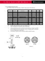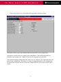
1
BQSBTS
User's Manual
April 2005
Revision 2.49
12500 TI Boulevard
Dallas, Texas 75243
Tel: 214-480-6083
Fax: 214-480-6400
Table of Contents
1 FEATURES AND SPECIFICATIONS ..................................................................................................................5
1.1 INTRODUCTION .....................................................................................................................................................5
1.2 FEATURES .............................................................................................................................................................5
1.3 TESTER SPECIFICATIONS .......................................................................................................................................5
2 UNPACKING AND INSPECTION .....................................................................................................................6
3
INSTALLATION AND SETUP ...........................................................................................................................7
3.1 MINIMUM SYSTEM REQUIREMENTS ......................................................................................................................7
3.2 INTERFACE CONNECTIONS ....................................................................................................................................7
3.2.1 Test Head Fixture Interface..........................................................................................................................9
3.2.2 Programmable Power Supply Connections ................................................................................................10
3.2.3 Electronic Load Connections......................................................................................................................10
3.2.4 Computer to Test System Interface .............................................................................................................10
3.2.5 Remote Interface Connections ....................................................................................................................11
3.3 GPIB SETUP RECOMMENDATIONS ......................................................................................................................11
3.4 SYSTEM POWER-UP.............................................................................................................................................13
3.5 SOFTWARE INSTALLATION — BTESTER SOFTWARE ...........................................................................................14
3.6 REFERENCE TEST ................................................................................................................................................14
4 TEST HEAD FIXTURE.........................................................................................................................................15
4.1 CONNECTION OF DEVICES UNDER TEST (DUT)..................................................................................................15
5 TESTING ................................................................................................................................................................16
5.1 INITIALIZATION ..................................................................................................................................................16
5.2 DEFAULT PARAMETERS ......................................................................................................................................18
5.3 START TESTING.................................................................................................................................................20
5.3.1 Self-Test Description ..................................................................................................................................22
5.3.2 Start and Stop Functions.............................................................................................................................23
5.3.3 Tester Limits .............................................................................................................................................23
5.4 PASS/FAIL STATUS .............................................................................................................................................24
5.4.1 Data Logging ..............................................................................................................................................24
5.4.2 LCD Display ...............................................................................................................................................24
5.4.3 LED Display ...............................................................................................................................................24
6 SPECIFIC TEST DESCRIPTIONS FOR BQ2040..............................................................................................24
6.1 BQSBTS FIELD DESCRIPTIONS OVERVIEW FOR BQ2040.....................................................................................24
6.1.1 Initial Device Configuration.......................................................................................................................24
6.1.2 Battery Data ...............................................................................................................................................25
6.1.3 EEPROM Block Data .................................................................................................................................26
6.1.4 Charging Information.................................................................................................................................26
6.1.5 Tester Limits ...............................................................................................................................................28
6.2 BQSBTS OPERATION OVERVIEW FOR THE BQ2040.............................................................................................29
6.2.1 Module Testing ...........................................................................................................................................29
6.2.2 Module Verify .............................................................................................................................................30
6.2.3 Pack Test.....................................................................................................................................................31
6.2.4 Pack Verify .................................................................................................................................................32
7 SPECIFIC TEST DESCRIPTIONS FOR BQ2060..............................................................................................35
7.1 THEORY OF OPERATION FOR BQ2060..................................................................................................................38
7.1.1 Module Testing ...........................................................................................................................................39
7.1.2 Module Verifying ........................................................................................................................................41
2
7.1.3 Pack Testing ...............................................................................................................................................41
7.1.4 Pack Verifying ............................................................................................................................................43
8 SPECIFIC TEST DESCRIPTIONS FOR BQ2063..............................................................................................44
8.1 THEORY OF OPERATION FOR BQ2063..................................................................................................................46
8.1.1 Module Testing ...........................................................................................................................................46
8.1.2 Module Verifying ........................................................................................................................................48
8.1.3 Pack Testing ...............................................................................................................................................48
8.1.4 Pack Verifying ............................................................................................................................................51
9 SPECIFIC TEST DESCRIPTIONS FOR BQ2083..............................................................................................51
9.1 THEORY OF OPERATION FOR BQ2083..................................................................................................................52
9.1.1 Module Testing ...........................................................................................................................................53
9.1.2 Module Verifying ........................................................................................................................................55
9.1.3 Pack Verifying ............................................................................................................................................55
10 SPECIFIC TEST DESCRIPTIONS FOR BQ2085............................................................................................55
10.1 THEORY OF OPERATION FOR BQ2085................................................................................................................56
10.1.1 Module Testing .........................................................................................................................................57
10.1.2 Module Verifying ......................................................................................................................................59
10.1.3 Pack Verifying ..........................................................................................................................................59
11 SPECIFIC TEST DESCRIPTIONS FOR BQ2084............................................................................................59
11.1 THEORY OF OPERATION FOR BQ2084................................................................................................................60
11.1.1 Module Testing .........................................................................................................................................60
11.1.2 Module Verifying ......................................................................................................................................62
11.1.3 Pack Verifying ..........................................................................................................................................62
12 SPECIFIC TEST DESCRIPTIONS FOR BQ20862..........................................................................................62
12.1 THEORY OF OPERATION FOR BQ20862..............................................................................................................63
12.1.1 Module Testing .........................................................................................................................................64
12.1.2 Module Verifying ......................................................................................................................................65
12.1.3 Pack Verifying ..........................................................................................................................................65
13 SOFTWARE UPGRADES ................................................................................................................................65
14 REVISION HISTORY .........................................................................................................................................66
14.1 DOCUMENT REVISION HISTORY .......................................................................................................................66
14.2 BQSBTS EMBEDDED FIRMWARE REVISION HISTORY ......................................................................................67
14.2.1 Embedded Firmware for testing the bq2092, bq2040, and bq2945..........................................................67
14.2.2 Embedded Firmware for Quick Verify of bq2092, bq2040, and bq2945 ..................................................68
14.2.3 Embedded Firmware for testing bq2060 ..................................................................................................68
14.2.4 Versions for testing the bq2060 and bq2063 ............................................................................................69
14.2.5 Versions for testing the bq2083 and bq2085 ............................................................................................69
14.2.6 Versions for testing the bq2084 ................................................................................................................69
14.2.7 Version for testing the bq20862.................................................................................................................69
15 WARRANTY ......................................................................................................................................................70
APPENDIX A - TEXAS INSTRUMENTS SYSTEM BUS TEST SYSTEM PACKING LIST..........................71
APPENDIX B - ERROR CODE DEFINITIONS FOR BTESTER BQ2040 / BQ2060 .......................................72
ERROR CODE DEFINITIONS FOR BTESTER BQ208X GAS GAUGE’S V1.0..............................................73
3
APPENDIX C - QUICK VERIFY EMBEDDED SOFTWARE (BQ2040, 2092, AND 2945 ONLY).................75
APPENDIX D - CHANGING THE DATE AND TIME ON THE SBTS .............................................................76
APPENDIX E – SBTS CALIBRATION..................................................................................................................80
TEXAS INSTRUMENTS TERMS AND CONDITIONS FOR SALES OF SBTS PRODUCTS ......................81
4
1 Features and Specifications
1.1 Introduction
The Smart Battery Test System from Texas Instruments is designed to test, Calibrate, and
program up to four electronic smart battery modules or packs in parallel. The electronic
modules and packs must conform to the System Management Bus Specification.
The system is currently designed to test bq2092, bq2945, bq2040, bq2060, bq2063, bq2083,
bq2084, bq2085, and bq20862-based modules. This system can test the electronic modules
prior to pack installation or in the pack provided that module calibration has been completed.
1.2 Features
•
Module test or in-pack testing of smart battery modules
•
Programs and calibrates smart battery modules
•
Monitors temperature for accurate calibration of modules
•
Computer control of electronic load and power supply via RS-232 or IEEE-488 ports
•
Increases test efficiency by testing four modules in parallel
•
Test System software flexible for smart battery module upgrades
•
Test software is Windows 3.1,Win 95, Win 98, and Win ME compatible
•
Test software is Windows XP compatible for the bq2083, bq2084 and bq2085
•
PC interface for data logging and device programming
•
Stand-alone test capability with PASS/FAIL LED indicators
•
Liquid crystal display for Test System status
1.3 Tester Specifications
AC Input: 110V to 240V, 50/60 Hz
Analog Inputs: ± 6V
Digital Inputs: 0 to + 5V
SMBus Interface: SMBus v 1.0 compliance
Remote Control Port: 0 +5V logic levels
Maximum Battery Voltage for Power Supply: 20V, or 40V for bqSBTS-005 only
Maximum Charge Current from Power Supply: 3A
Maximum Discharge Current from Electronic Load: 3A
5
Note: Values greater than these limits entered into the bqSBTS system software or connected to
the hardware may cause permanent damage to the bqSBTS.
2 Unpacking and Inspection
In the test system shipping box you will find a packing list. Identify the version number on the
packing list you ordered and verify that all items required for your system are present. Notify
Texas Instruments of any discrepancies immediately. See Appendix A for packing list example
and configurations.
Verify that all the items received are in good condition and no damage has occurred during
shipment. Notify Texas Instruments immediately of any damage that has occurred during
shipment.
6
3 Installation and Setup
3.1 Minimum System Requirements
Computer: PC or compatible 486 66 MHz
Operating System: Windows 95, 98 or Windows 3.1
Video: Super VGA – 1024 x 768 minimum resolution
RAM: 16 Mbytes
Hard Drive Space: 5 Mbytes
RS-232 Port: 1 available
For bq208X gas gauges: Windows XP may be used
3.2 Interface Connections
The Test System requires test probe connections for each module to be tested and interface
connections to the Power Supply, Electronic Load and the computer. Each of these
connections are specified in this section.
Referring to the system connection diagram below:
1. The Power Supply is connected to the GPIB connector on the back of the SBTS. (The GPIB
address of the power supply is 15).
2. The Active Load is also connected to the GPIB connector. (The GPIB address of the active
load is 08).
3. The host PC is connected to the Controller Input which is RS-232. Connect the Host PC to
the controller input with a null modem cable (communications crossed Rx to Tx and Tx to
Rx).
7
8
3.2.1 Test Head Fixture Interface
The test head interface for Smart Battery Module testing requires the following:
Device Under
Test Port Pin
1
2
3 ***
4
5 ***
6 **
7 ***
8
9 *
10
11
12 *
13
14 *
Function
Input
Input/Output
Output
Input/Output
Output
Output
Input/Output
Input
Output
Output
N/A
Output
N/A
Output
Description
(VCC) Module Voltage
SMBus Clock
EEPROM Supply Voltage
SMBus Data
EEPROM Clock (SCL)
Temp. Sensor (LM335AZ)
EEPROM Data (SDA)
Temperature Sense In
Pack - / Gnd
Temp. Sensor GND
No Connection
Battery + / Pack +
No Connection
Battery -
Color
Code
Brown
Red
Orange
Yellow
Green
Blue
Violet
Gray
White
Black
N\A
Red
N\A
White
Wire
Gauge
24 AWG
24 AWG
24 AWG
24 AWG
24 AWG
24 AWG
24 AWG
24 AWG
20 AWG
24 AWG
N/A
20 AWG
N/A
20 AWG
Pack
Test
X
X
X
X
Note: See Appendix C for sample schematic that identifies test points.
X
Denotes signal required for Pack Test or Module Test.
*
These wire gauges are required for these connections.
**
Only one temperature sensor should be wired to one Device Under Test (DUT)
port. Wiring more than one temperature sensor to additional ports will produce
erroneous temperature measurements.
***
Not needed for bq2060, bq2063, bq2083, bq2084 or bq2085 testing.
206044-1
9
Module
Test
X
X
X
X
X
X
X
X
X
X
X
X
3.2.2 Programmable Power Supply Connections
Power supply cable should not exceed 5 ft. in length and should use a minimum of 18
AWG wire. Note: Make sure unit is turned off before connecting AC power cord.
Pin 1 = No Connection
Pin 3 = No Connection
Pin 2 = V- (Black wire)
Pin 4 = V + (Red wire)
Connect Power Supply Power Cable with female connector shown below to Test System
and Power Supply Connect AC power cord. Connect GPIB cable to GPIB connector on
the back of the SBTS and to the Power Supply.
P/N 206060-1
3.2.3 Electronic Load Connections
Electronic load cable should not exceed 5 ft. in length and should use a minimum of 18
AWG wire. Note: Make sure unit is turned off before connecting AC power cord.
Pin 1 = Load (White wire)
Pin 2 = Load Return (Black wire)
Pin 3 = No Connection
Pin 4 = No Connection
Connect the Electronic Load cable with the male connector shown below to the test
system and to the load. Connect AC power cord. Connect GPIB cable to GPIB connector
on the back of the SBTS and to the Load.
P/N 206429-1
3.2.4 Computer to Test System Interface
Connect the RS-232 null modem cable from the COM port on the back the computer to the
“Controller Input” port on the rear of the test system.
10
3.2.5 Remote Interface Connections
The remote interface is to allow the start and stop switches and the pass/fail LEDs to be mounted
on a remote fixture such as a test head fixture to allow control of testing at the test site. To
connect to the remote port, follow connection chart below. Switches should be momentary and
normally open types. LED current is limited to approximately 60 mA max. All of the LED
anodes should be connected to pin 7. The LED cathodes should be connected to the appropriate
pin designated below.
Remote Connector—15-Pin db
Pin #
Pin#
1- Start switch N.O.
3 - No Connection
5 - DUT #1 fail, Red LED
7 - DUT #3 fail, Red LED
9 - Stop Switch N.O.
11 - No Connection
13 - DUT #2 pass Green LED
15 - DUT #4 pass Green LED
2- GND
4 - +5V for LEDs
6 - DUT #2 fail, Red LED
8 - DUT #4 fail Red LED
10 - No Connection
12 - DUT #1 pass Green LED
14 - DUT #3 pass Green LED
Notes: Pins 3, 10, and 11 are not connected
RED LED = HLMP0150 with 1K limiting series resistor
GREEN LED = HLMP3507 with 2K limiting series resistor
5v
bqSBTS
LED
75Ω
Resistor
3.3 GPIB Setup Recommendations
The GPIB setup is only available in “bqSBTS Test System Embedded Software V 1.9.6. Beta
and later. To install any new embedded software, follow the bqUPDATE instructions in
section 13, Software Upgrades.
Most GPIB devices do not request all the settings listed below. They are listed here to
illustrate GPIB port configurations that the bqSBTS may potentially require.
11
Load:
AC Input: 110V, 120V, 220V and 240V, 48-63Hz (4 internal switch options)
GPIB Configuration:
Primary address: 08
Address mode: Primary
Secondary address: 0 or None
End of identify: EOI + CR
EOS byte: 13 decimal
Terminate read on EOS: Yes
Set EOI with EOS on write: Yes
Set EOI on last byte of write: Yes
Time-out setting: 1 second
Suggested specifications
Low range should be 0 to 5A or more for maximum accuracy
Suggested accuracy 0.1% ±7.5mA
Suggested resolution: 1.6mA
Power supply:
AC Input: 110V, 115V and 230V (3 internal switch options)
GPIB configuration
Primary address: 15
Address mode: Primary
Secondary address: 0 or None
End of identify: EOI + CR
EOS byte: 13 decimal
Terminate read on EOS: Yes
Set EOI with EOS on write: Yes
Set EOI on last byte of write: Yes
Time-out setting: 1 second
Suggested specifications
Readback resolution:
Voltage: 2.4mV
Current: 1.4mA
Readback accuracy:
Voltage: 0.3%
Current: 0.12%
Program resolution:
Voltage: 4.7mV
Current: 1.4mA
Program accuracy:
Voltage: 0.1%
Current: 0.12%
12
The specifications listed above are representative of the equipment that has been tested with
the bqSBTS. Although these specifications are not listed as requirements, the module
calibration accuracy depends on the accuracy of the electronic load and power supply used.
The bqSBTS is designed to communicate with any load or power supply that conforms to the
SCPI standard. Because some equipment manufacturers use special non-SCPI-standard
formats for specialized instructions not defined in the standard, the bqSBTS has been tested
with the following equipment for communications compatibility and functionality:
Xantrex HPD 30-10 GPIB Power Supply
Xantrex HPD 60-5 GPIB Power Supply
Tektronix PS2511G GPIB Power Supply
Hewlett Packard 6060B GPIB Electronic Load
Hewlett Packard 6063B GPIB Electronic Load
Amrel PEL150-1 Electronic Load (manual configure in constant-current mode)
Amrel EL60-30-150 Electronic Load
Hewlett Packard E3634A GPIB Power Supply
Note: The bqSBTS has been tested with the Kikusui PLZ153W Electronic Load and does not
communicate with that equipment.
3.4 System Power-up
After all connections are made, make sure the power switch is in the off position and plug in the
AC cord to 120 VAC 60 Hz source to the test system. Turn on the Test System with the AC
power switch located on the left rear of the test system when facing the unit. During power up,
the test system performs a “Self- Test.” The test system should always be the last unit turned
on and the first to be turned off. The self-test consists of communication checks of the
Programmable Power Supply and the Electronic Load, calibration checks, and other internal
checks. Make sure that nothing is connected to the DUT ports before power-up.
When “Self-Test” passes, the LCD displays the following:
System is Ready
Send EEPROM Data
Send Configuration
Status: Waiting
All of the LEDs should be on at this time.
If self-test “Fails,” verify nothing is connected to the DUT ports. Verify the interface connections
have been made correctly. Power down system and power up again and if self-test continues to
fail, contact Texas Instruments. Please refer to the Self Test Description in section 5.3.1
13
3.5 Software Installation — Btester Software
There is a different version of the Btester software for each gas gauge. This example is for the
bq2040. You should make backup disks prior to installing software. This will ensure you have
copies of the software in the event that something happens to the original disks.
Install disk #1 in the A: drive.
Run “setup.exe” from the A: drive.
The software should begin loading and prompt for the next disk when finished loading disk #1.
Install disk #2 in the A: drive when prompted. After disk #2 is finished loading, install disk #3
when prompted in the A: drive. Follow instructions on the screen. The software will prompt for
the com port setup. Make sure the com port selected is available.
Baud rate and data settings are as follows: Baud “19200”, “8” data bits, “n” parity, “1” stop bit.
19200, 8, n, 1
If you get a “run time” error when starting the software, there is probably a conflict with the com
port settings. Re-install the software and choose a different com port.
Copy “example” from the Tester Embedded Software disk to C:\BTESTER\CONFIG\bq2040, or
to the directory you chose during installation. This file is used to perform the reference test
described in section 3.6. If you are using Btester software, version 1.7.0 or greater, “example” is
copied automatically during installation.
NOTE: Configuration file changes should be made within Btester software only.
Changing files outside of the Btester program will corrupt the files and make them
unusable.
3.6 Reference Test
The reference module is a module designed to test the integrity of all four of the Device
Under Test Ports prior to connecting the test head fixture. The reference test should be
performed anytime the Device Under Test (DUT) ports are in question. Perform “Reference
Test” following the instructions below. Note, however, that the reference test cannot be
tested with bq2060 software or any software which is version 2.25 or higher.
•
Make sure the Load, Power Supply, Computer, and Test System are all turned on.
•
Connect the reference test module to DUT port number one. (Or the port in question.)
•
Initialize the test software described in section 5.1.
14
•
For device selection, select “bq2040” and select “example” as the configuration file.
Older versions of the software do not automatically install the example file. Versions 1.7
and later automatically install it as Btester\Config\bq2040\example.
•
The configuration file for this test should not be changed or the reference test module
may not pass the reference test.
•
Disable the DUT ports where the reference module is not connected and enable the port
where the reference module is connected using the “System Test” screen.
•
Click on the “Start” icon to load the configuration into the test system.
•
Wait for the LCD to indicate DUT 1: READY TO START.
•
Push the “Start” button on the test system front panel to test the reference module.
Note: Do not perform a “module test” on the reference module. The reference modules are writeprotected and cannot be calibrated.
4 Test Head Fixture
The Test Head (test fixture) can be constructed following the interface connection chart in
section 3.2.1 using a schematic and assembly drawing for the module to be tested. It is
recommended that test head cables not exceed 10 feet in length. Spring-loaded test pins are
recommended for module testing. Connection of test head to modules requires precision contacts
to ensure good electrical contact. It is recommended that pack test be performed in a pack
connector used by the customer for final product. For testing the bq2060 using the embedded
firmware with revision number less than V2.30 with individual cell voltages, connect pin 12
(Battery+ / Pack+) to all cell voltage inputs. For testing the bq2060 using embedded firmware
v2.30 or greater you must install 200 ohm 0.1% resistors to the test head to simulate individual
cells for 2, 3, or 4 cell LION configurations and a diode (1N5820 or equivalent) placed between
Pack- and the BQSBST Device Under Test Port Pin 9 defined in section 3.2.1 Test Head Fixture
Interface for current measurement accuracy during the Icc test. No resistors are required for
testing NiMH or 1 cell configurations. Refer to section 7 for bq2060 specific issues and a
connection diagram. For testing the bq2063, you must install 200 ohm 0.1% resistors to the test
head to simulate individual cells for 3, or 4 cell LION configurations. Refer to section 8 for
bq2063 specific issues and connection diagram. For testing the bq2083, bq2084 or bq2085 you
must install 200 ohm 0.1% resistors to the test head to simulate individual cells for 2, 3, or 4 cell
LION configurations and a diode (1N5820 or equivalent) placed between Pack- and the
BQSBST Device Under Test Port Pin 9 defined in section 3.2.1 Test Head Fixture Interface for
current measurement accuracy during the Icc test. Refer to sections 9, 10, 11 and 12 for specific
issues and connection diagrams.
4.1 Connection of Devices Under Test (DUT)
Place modules or packs into test head fixture and make contact to the appropriate test points.
15
5 Testing
For detailed testing descriptions, refer to the later chapters, which cover the various devices in
detail.
There are four types of test modes:
• Module Test
• Module Verify
• Pack Test
• Pack Verify
During Module/Pack testing, the test system performs calibration, writes EEPROM or FLASH
data, and checks additional parameters.
During Module/Pack verification, no data is written. The test system verifies that all data is
correct, based on the configuration of the module/pack.
Testing can be started after the reference test has been completed for the first time. To perform
the reference test, see section 3.6.
Module tests must be performed before pack tests so that complete calibration and functional
testing is performed prior to pack assembly. During bq2040, bq2092 and bq2945 module
testing, all data is written to EEPROM. However, this is not done during pack testing in order to
make the test process more efficient and because certain EEPROM write locations cannot be
written through the SMBus. On the bq2060, bq2063, bq2083, bq2084, bq2085, and bq20862
pack testing cannot be tested first because voltage calibration requires multiple calibration points
and voltage cannot be easily changed in packs.
Be sure to set the charge and discharge current to a high number (as close to 2 amps as possible)
without exceeding the 3A test set limit. This will insure accurate calibration and no VFC
timeout.
5.1 Initialization
Double-click the bqSBTS icon to start the test program. The display shown below should be
present. You can start this from the START\PROGRAM\BTESTER under Windows or from
BTESTER.exe in the directory you chose at installation.
•
Enter “bmrq” in the password field. When the program starts, the following should be
displayed:
16
•
•
•
•
•
•
Enter “bmrq” for the password. This is the initial default password.
Select the correct Benchmarq device to be tested in the device field. (For the reference test,
select the bq2040).
Select the configuration file. (For the reference test, select the example program).
Enter the starting serial number for the test sequence.
Enter the Manufacturing date.
Click on Ok. Then click on “Module Configuration.”
17
5.2 Default Parameters
The module configuration screen should now be present as shown below. Check and verify
that the part number and the configuration file indicated on top of the window bar is correct.
Module testing can now be performed. The test system is locked at this point, and no
changes to the configuration can be performed without unlocking the system. If you have
selected the configuration file you are going to use and you want to start testing modules, you
can skip to section 5.3 and start testing.
To unlock the system, you must enter the master password. Go to edit\unlock on the menu
bar. The initial master password is set to “bmrqm”. Enter “bmrqm” in the password field to
unlock the system.
Change configuration settings as needed and be sure to save the configuration when finished.
Some fields will turn red if the value entered is out of range. This allows you to enter values
above the normal range for a custom configuration. Certain fields will not allow entry above
a specified range. An out-of-range number entered in these fields will not be accepted.
18
Click on the “System Test” tab and the following display should be present.
This window allows you to enter min/max limits for the module you are going to test.
Enter the test system limits you require for this configuration. Then enable the module test
positions you are going to use. Enable LED test if you are going to test the LEDs.
When finished entering configuration data, select “save as” from the “File” menu and enter a file
name for this configuration. Each time you change a configuration and save the configuration
file, the system test limits are also saved in the configuration file. You are now ready to begin
testing.
19
5.3 Start Testing
At this point, power to the test system, power supply, and electronic load should be on.
Select “Module Test” tab to begin testing. The following window should be displayed. This
window displays the status or results of testing or verify.
•
•
•
•
•
•
•
Module Status: Displays the status of each Device Under Test Port (DUT). Red is an error
condition; Green is OK; Yellow is IDLE; Blue is TESTING.
Statistics: Displays and keeps running totals of modules tested.
Last Good Serial Number: Displays the last good serial number tested.
Modules Tested: Displays the total number of modules tested.
Modules Passed: Displays the total number of passed modules.
Modules Failed: Displays the total number of failed modules.
Modules Passed Per Hour: Displays a current average of the number of modules passed per
hour.
20
Click on the “Start” icon to download the configuration information to the Test System.
The LCD on the test system should display the following:
Configuration Received
EEPROM Data Received
The LCD then clears and displays the following:
DUT #1:
DUT #2:
DUT #3:
DUT #4:
Ready to Start
Ready to Start
Ready to Start
Ready to Start
Place modules to be tested in the test head fixture locations to be used.
Press the “Start” button on the test system front panel.
The LCD displays the test status as it proceeds through the test steps. If a module fails, the test
system stops testing that module and continues testing the remaining modules that are active.
The LCD displays an error message for the module that has failed. If a power supply or potential
harmful test parameter fails then all testing is halted. Failure data will be displayed & the green
Start button will have to be pressed to get back to the “DUT Ready” state. Troubleshoot the
problem and resume testing.
When the test is completed, the test system sends all the test information to the computer and
displays results in the tester log. “Module Tests” and “Module Verify” field descriptions are:
TME: Time of test
MOD: DUT #1–4
SSN: Serial number of passed device
LVC: VCC low voltage from tester
LIC: Low ICC from tester
*LBV: Low battery voltage from DUT
CCR: Current read from power supply
DAT: Date of test
STS: Error status
BSN: Serial number of failed device
MVC: VCC high voltage from tester
MIC: Max ICC from tester
MBV: High battery voltage from DUT
(*LBV & MBV are always 0 when testing bq2060 and bq2063.)
The “STS” field displays an error code related to an error status. See Appendix B for
descriptions of error codes.
If you selected “Pack Test” instead of module test, the Test log field displays the test log
categories described below.
TME:
MOD:
SSN:
DCR:
DBV:
Time of test
DUT #1–4
Serial number of passed device
Device current read
Device battery voltage
DAT:
STS:
BSN:
PCR:
PBV:
21
Date of test
Error status
Serial number of failed device
Power supply current read
Power supply battery voltage
5.3.1 Self-Test Description
The self-test is performed each time the system is powered up. The self-test tests the power
supply and load by connecting them together through the DUT ports. This confirms
communication with the load and power supply and verifies that the system is functional.
Nothing should be connected to the DUT ports during power-up.
The bqSBTS only requires its internal A-to-D converter for Self-Test Voltage Calibration
Verification and Temperature Calibration. If Self-Test fails with a certified calibrated power
supply and load, then the bqSBTS could be out of calibration. During the Self-Test, the
voltage communicated from the power supply is compared with the A-to-D converter of the
bqSBTS. If there is greater than 1% difference, then the Self-Test fails. To have the bqSBTS
system re-calibrated, please contact your local Texas Instruments office.
Note: Do not connect anything to any of the DUT connectors while the Self Test is running.
The Object of the Self test that the SBTS performs each time it powers up is to check for
possible inaccuracies in the power supply and load, and to check for problems in the logic
circuitry that handles the Power Supply and Load switching for each DUT port. Two
procedures are performed to accomplish this.
1. The first procedure uses current to check the load and power supply reported current
accuracy and the SBTS logic circuitry used to connect voltage and load to the module. This
is done by connecting the load to the power supply through all the FET switches in the SBTS
that are used to pass current through a module during a normal module test or verify. This
current is passed through all 4 DUT ports separately. The current is read from the load and
the power supply for each port and checked. The routine checks for discrepancies in the
reported load current and the power supply current while setting the power supply to 2.1
Amps and the load to 2.0 Amps. It will fail the test if either power supply or load report a
current back that is greater than 5% off of 2.0 Amps or if the reported currents are different
by more than 2%.
2. The second procedure uses voltage to check voltage accuracy and the logic circuitry that
applies battery voltage to the module during a normal module test or verify. Each DUT port
is checked separately with both 13V and 5V. The SBTS uses an internal voltage divider and
an ADC to measure the voltage and compares it to the voltage reported back from the power
supply. If the difference between the voltages is greater than 1% then the test fails.
Reported Errors and their Meanings:
1. PS Read Problem: The SBTS could not communicate with the power supply.
Check the GPIB or the power connectors running from the SBTS to the power supply. If the
power supply current limits then this could be a result of crossed wires, an external short, or
by an internal circuitry failure in the power supply or the SBTS.
2. Load Read Problem: The SBTS could not communicate with the load.
Check the GPIB or the power connectors running from the SBTS to the load.
3. PS Failed Cur Cal Test: The power supply was more than 5% off of the 2.0 Amp
requested current.
The power supply is either out of calibration or there is a circuitry problem. A circuitry
problem could be caused by power cables that are not connected properly on the load or the
power supply or an internal SBTS, load, or power supply circuitry failure.
22
4. Load Failed Cur Cal Test: The load was more than 5% off of the 2.0 Amp requested
current.
The Load is either out of calibration or the load power connector is not connected properly.
5. PS and Load Failed Cur Cal Test: The power supply and load reported currents are
more than 2% different.
The load, power supply, or both are out of calibration or there is an internal circuitry failure
in the SBTS.
6. PS and Load Failed Volt Cal Test: The power supply reported voltage was more than
1% different from the voltage read from the SBTS ADC voltage.
The power supply is either out of calibration or there is an internal circuitry failure in the
SBTS.
5.3.2 Start and Stop Functions
The Start icon on the module test screen is used to download the configuration file to the test
system.
The Stop icon clears the configuration file from the test system.
5.3.3 Tester Limits
The “SYSTEM TEST” screen displays the limits that the tester uses during module or pack
testing. The limit fields are described below.
Min/Max Battery Voltage: Sets the voltage range for fully charged and discharged packs.
Number of Voltage Calibration Points: Set to 3; used to calibrate pack voltage.
Max Charge and Discharge: Maximum charge and discharge current in milliamps used
during test to calibrate current monitoring and to remaining capacity.
Min/Max VCC: Minimum and Maximum VCC limits allowed over the battery voltage
range.
Min/Max ICC: Minimum and Maximum input current allowed over the range of battery
voltage.
23
5.4 Pass/Fail Status
5.4.1 Data Logging
Data is logged on the computer monitor and in a data file. The file will be placed into a
default file named with the current system date, unless you specify a file name under the
LOG MENU. You can also append data to an existing file by choosing “open” under the
LOG MENU. Example default file name: (L980328) March 28, 1998.
5.4.2 LCD Display
The LCD display indicates the status of devices under test, and is used to display the tester
status in other test conditions or while downloading configuration files.
5.4.3 LED Display
LEDs indicate a pass or fail condition during testing. Green LEDs indicate passing devices
and red LEDs indicate failing devices. If a device is not available, the LEDs for that device
are red.
6 Specific Test Descriptions for bq2040
6.1 bqSBTS Field Descriptions Overview for bq2040
6.1.1 Initial Device Configuration
Flags 2: Refer to the data sheet for information on this register. The main functions for
this register are chemistry selection (Li-Ion or NiMH) and Display Mode (Relative or
Absolute).
Sense Resistor: This should be set to the Ideal Sense Resistor Value in mΩ.
Digital Filter: Any voltage integrated below this value will not alter the battery
capacity. This value is in μV.
Battery Voltage Divider: The pack voltage is divided down by a resistor-divider to
represent the average voltage for one nickel chemistry cell or half of a lithium ion cell.
RBAT+ is the upper resistor in the voltage divider connected to BATT+. RGND is the
lower resistor in the divider connected to ground. Refer to the bq2040 data sheet for
more information.
R
+ RGND
Ratio = BAT +
RGND
24
Pack Default Capacity: This is only used during a Pack Test. During Pack Test, this
value will be inserted into the RAM location for Remaining Capacity. Since the
module is in a pack and will not lose power after a test, this value can be used to put an
approximate capacity in for the battery in which the module is installed. It is not critical
since the bq2040 will learn the correct capacity with a full learning cycle. During a
Pack Verify, the Remaining Capacity is temporarily stored and reinserted in the RAM
location for Remaining Capacity once the verify is complete, so the pack default
capacity is not used.
Note: This field is only visible with a Pack Verify or Test. It is not used during
Module Test or Verify.
6.1.2 Battery Data
Design Capacity: Theoretical design capacity of a new battery pack.
Design Voltage: Theoretical nominal total voltage of a battery pack. This is also the
middle voltage the bqSBTS uses in the 3-point voltage calibration (Maximum Battery
Voltage, Design Voltage, and Minimum Battery Voltage).
EDV1 (End-of-Discharge 1): If pack voltage falls below EDV1, then the display flashes
one LED and the EDV1 flag is set. The Remaining Capacity is written to (Battery Low
Percentage * FCC) unless Remaining Capacity is already below this value.
EDVF (End-of-Discharge Final): EDVF bit is set and the display is cleared if the pack
voltage falls below this value. Remaining Capacity is also set to 0. The EDV thresholds
and Battery Low Percentage should be programmed such that Remaining Capacity
reaches 0 before the EDVF bit is set for proper learning.
Remaining Capacity Alarm: When the Remaining Capacity (RM) falls below this
value, then the Remaining Capacity Alarm flag is set.
Specification Information: SMBus specification revision the device supports. All this
value should always be programmed to “00 00 01 00” (IP=0, V=0, Major =1, zeroes
represent non-revision 1.0 compliance to SMBus specifications. For the bq2040,
Minor=0).
Serial Number: Serial number of the pack. When combined with manufacturer’s
name, device name, and manufacture data, it uniquely identifies a battery. This value
will automatically increment with each Module or Pack Test but is not modified by a
Verify. The software can be set up such that this value will not increment on a failed
test using the Serial Number pull-down menu.
Self-Discharge Rate: The battery capacity will be decreased by the percentage set in
this field each day at a temperature range of 20°C to 30°C. For every 10°C above this
25
temperature range, the self-discharge rate doubles. For every 10°C below this range,
the self-discharge rate is halved.
Remaining Time Alarm: When the average time to empty falls below this value, then
the remaining time alarm bit is set.
Initial FCC Value (Fully Charged Capacity): Sets the initial value of the Fully
Charged Capacity. This value is continuously updated with full discharge (learning
cycles) and should be slightly less than Design Capacity to ensure proper capacity
learning.
Busy flag: This field controls RAM access. A “0” in this field indicates protected
access. A “1” indicates unprotected access. When protected, 0x00-0x04 can be read
and written, the SMBus specification commands are read only, and the rest of the RAM
is read / write protected. When unprotected, all memory locations can be accessed.
Battery Low Percentage: Battery Low Percentage (BLPCT) is used to ensure proper
capacity learning during a complete learning cycle. This is the theoretical percentage of
capacity of the battery at EDV1. When EDV1 is reached, then the remaining capacity
will be written to BLPCT * FCC. If this value is reached before EDV1, then further
decrementing of Remaining Capacity will not occur until EDV1 is reached.
6.1.3 EEPROM Block Data
Manufacturer Name: This field can be any 11 characters in ASCII format (Example:
Texas Instruments).
Device Date: (YY/MM/DD) This field will default to today’s date but can be modified.
Device Name: This field can be any 7 ASCII characters (Example: bq2040).
Device Chemistry: This field can be any 5 ASCII characters (Example: NIMH).
Manufacturer Data: This field can be any 5 Decimal representations of ASCII
characters (Example: 066 077 082 081 translates to BMRQ).
6.1.4 Charging Information
Fast Charge Rate: This is the maximum charging current the bq2040 broadcasts.
Charging Voltage: The maximum charging voltage the bq2040 broadcasts should be
the same value as the Maximum Battery Voltage in Tester Limits.
Trickle Charge Current: This is the current the bq2040 broadcasts in maintenance
(trickle) mode.
26
Maximum Charge Temperature: The maximum allowable temperature for continued
charging. When the pack reaches this temperature, the broadcast current is set to 0.
Delta Temperature: The maximum allowed temperature change over the time set in
the Δt Timer (ΔT/Δt) during charging. If this value is exceeded in the time set in the Δt
Timer, then the broadcast charging current is set to zero, the Fully Charged bit is set,
and the Remaining Capacity is set to FULPCT. For Lithium batteries, usually the ΔT is
set to the maximum value of 4.6°C to prevent a ΔT/Δt termination.
Full Charge Percentage (FULPCT): If a current taper or ΔT/Δt termination occurs
and the CC bit is set in Flags 2, then the Remaining Capacity is set to FULPCT * FCC.
The broadcast charging current is also set to maintenance (trickle) current. Remaining
Capacity is not set to FULPCT * FCC if the CC bit is not set or if the Remaining
Capacity is already above this value.
Low Efficiency: When the Relative State of Charge (0x0d) is above FULPCT then the
battery is charged at the Low Efficiency rate.
High Efficiency: When the Relative State of Charge (0x0d) is below FULPCT then the
battery is charged at the High Efficiency rate.
Δt Timer for ΔT/Δt: The amount of sample time used in ΔT/Δt calculation during
charging. If the temperature change exceeds ΔT (T = temperature) in this Δt (t = time),
then the broadcast charging current is set to zero, the Fully Charged bit is set, and
Remaining Capacity is set to FULPCT. Longer times are required for increased slope
resolution. For Lithium batteries, usually the Δt value is set to 20 seconds to prevent a
ΔT/Δt termination.
Hold Off Timer: ΔT/Δt detection is suspended while this timer is running. It starts
when the battery is being charged at greater than 255mA and is hotter than 25°C. When
it expires, ΔT/Δt detection resumes.
Initial Charging Current: The value that is put in the broadcast charging current
register immediately after the bq2040 resets. It remains at this current until the correct
charging current can be determined. This is usually set to a low value (Example:
100mA).
Taper Current Limit: An IMIN (taper current) termination occurs when charging
current is less than this threshold for at least 100 seconds while remaining non-zero and
while the pack voltage measurement remains greater than (Charging Voltage – 128mV).
Maximum Overcharge Threshold: This is a safety termination threshold. Once
Remaining Capacity =FCC and the battery continues to be charged to an amount greater
than this threshold, then the Fully Charged bit is set, and the broadcast charging current
is set to maintenance (trickle).
27
EDVF Charging Current: If voltage falls below EDVF, then the broadcast charging
current is set to this value.
Overload Discharge Current: If a discharge current exceeds this value, then EDV
detection is suspended.
6.1.5 Tester Limits
Minimum Battery Voltage: The lowest battery voltage that the bq2040 is expected to
operate.
Maximum Battery Voltage: The highest battery voltage that the bq2040 is expected to
operate.
Number of Calibration Points: This value should be set to 3 although it is never used
by the bqSBTS.
Maximum Charge Current: This should be the same current as the Fast Charge Rate.
This value is used by the bqSBTS as a charge current when Testing or Verifying
Current for modules or Testing Packs in the Charge Direction.
Maximum Discharge Current: This value is usually set to the same current as the Fast
Charge Rate. It is only used on Pack Test or Verify. The bqSBTS tries to test or verify
current calibration in the charge direction first. If the battery starts to taper, then the
current is reversed, and the Pack current calibration is tested or verified in the discharge
direction by this amount.
Minimum VCC Pass Voltage: The bqSBTS sets the battery voltage to the Minimum
Battery Voltage during the VCC ICC Test and reads the VCC. If it is less than this value,
then the bq2040 fails the test.
Maximum VCC Pass Voltage: The bqSBTS sets the battery voltage to the Maximum
Battery Voltage during the VCC ICC Test and reads the VCC. If it is greater than this
value, then the bq2040 fails the test.
Minimum ICC Pass Current: The bqSBTS sets the battery voltage to them Minimum
Battery Voltage during the VCC ICC Test and reads the ICC. If it is less than this value,
then the bq2040 fails the test.
Maximum ICC Pass Current: The bqSBTS sets the battery voltage to them Maximum
Battery Voltage during the VCC ICC Test and reads the ICC. If it is greater than this
value, then the bq2040 fails the test. This value is usually set to 250μV or greater
depending on the current required by the other circuitry in the module being tested.
28
6.2 bqSBTS Operation Overview for the bq2040
The procedures used to test and verify the bq2040 used the bqSBTS are complex. This
overview aims to minimize test time while ensuring a very thorough test.
6.2.1 Module Testing
VCC and ICC Test: This test is used to ensure the bq2040 does not exceed voltage and
current limits. The procedure is as follows.
1. Read EEPROM location 0x00 to verify part orientation in the test head fixture.
2. Set power supply voltage to 6.0 V at 35mA
3. If power supply current limits, then fail test due to excessive current.
4. Set power supply voltage to Maximum Battery Voltage.
5. Verify VCC does not exceed value set in Maximum VCC Pass Voltage.
6. Set power supply voltage to Minimum Battery Voltage.
7. Verify VCC does not fall below value set in Minimum VCC Pass Voltage.
8. Set power supply voltage to Maximum Battery Voltage.
9. Verify ICC does not exceed value set in Maximum ICC Pass Current.
10. Set power supply voltage to Minimum Battery Voltage.
11. Verify ICC does not fall below value set in Minimum ICC Pass Current.
EEPROM Test: This test writes the data from the Module Configuration Window
including nominal calibration values to the EEPROM. The nominal calibration values are
derived from the Sense Resistor and the Battery Voltage Divider fields in the Module
Configuration Window. They are then read to verify they are correct.
Voltage and Temperature Calibration: Voltage Calibration uses a 3-point sum of
squares algorithm to determine the offset and the voltage gain of the bq2040. All devices
under test (DUTs) are tested in parallel to reduce test time.
Calibration Limits & Procedure:
Gain Calibration: Calibrated gain must be 25% or less than the nominal gain.
Voltage Offset Calibration: Calibrated offset must be in the range of ± 125mV.
Temperature Offset Calibration: Calibrated offset must be in the range of ±12.7°K.
The procedure is as follows:
1.
2.
3.
4.
5.
6.
7.
Set battery voltage to Minimum Battery Voltage.
Read the bq2040 voltage.
Set battery voltage to the voltage read in Design Voltage.
Read the bq2040 voltage.
Set battery voltage to maximum Battery Voltage.
Read the bq2040 voltage.
Calculate the offset and gain
29
8. Read the temperature from the bqSBTS
9. Read the temperature from the bq2040
10. Calculate the temperature offset
Current Calibration: Current calibration corrects gain for Sense Resistor tolerance.
There are 2 gain factors. One is for Voltage to Frequency Converter (VFC) capacity
measurement, and the other is for VFC current measurement. LED testing is also
performed if enabled.
Calibration Limits & Procedure:
Sense Resistor Gain Calibration: Calibrated gain must be within 25% of the nominal gain.
The procedure is as follows:
1.
2.
3.
4.
5.
6.
Set current to maximum charge current.
If LED test enabled then beep and display each LED individually
Start 20-second bqSBTS timer and simultaneously read the raw VFC register.
Wait 20 seconds.
Read the raw VFC register.
Calculate the new gain for VFC current and capacity gain.
6.2.2 Module Verify
Module Verify does not alter any EEPROM locations. It only verifies that the part is
calibrated correctly and that the EEPROM matches the Module Configuration Screen
excluding the calibration and Serial Number values.
VCC and ICC Test: This test is used to ensure the bq2040 does not exceed voltage and
current limits. The procedure is as follows:
1. Read EEPROM location 0x00 to verify part orientation in the test head fixture.
2. Set power supply voltage to 6.0 V at 35mA
3. If power supply current limits then fail test due to excessive current.
4. Set power supply voltage to Maximum Battery Voltage.
5. Verify VCC does not exceed value set in Maximum VCC Pass Voltage.
6. Set power supply voltage to Minimum Battery Voltage.
7. Verify VCC does not fall below value set in Minimum VCC Pass Voltage.
8. Set power supply voltage to Maximum Battery Voltage.
9. Verify ICC does not exceed value set in Maximum ICC Pass Current.
10. Set power supply voltage to Minimum Battery Voltage.
11. Verify ICC does not fall below value set in Minimum ICC Pass Current.
EEPROM Test: This test reads the EEPROM data and compares it to the values from the
Module Configuration Window except for the values dealing with calibration and serial
number.
Voltage and Temperature Verify: Verifies the accuracy of the voltage and temperature
calibration values. All DUTs are verified in parallel to reduce test time.
30
Accuracy Limits & Test Procedure:
Voltage Accuracy: bq2040-read voltage must be within ±2% of the power supply voltage.
Temperature Offset Accuracy: Temperature offset must be within ±2.0°K of bqSBTS
temperature.
The procedure is as follows:
1. Set power supply voltage to Minimum Battery Voltage.
2. Read the bq2040 voltage.
3. Set power supply voltage to the voltage read in Design Voltage.
4. Read the bq2040 voltage.
5. Set power supply voltage to maximum Battery Voltage.
6. Read the bq2040 voltage.
7. Verify all voltages are within ±2% of power supply voltages.
8. Read the temperature from the bqSBTS
9. Read the temperature from the bq2040
10. Verify the bq2040 temperature is within ±2.0°K of the bqSBTS temperature.
Current Verify: Verifies the Sense Resistor gain accuracy. There are two gain factors.
One is for VFC capacity measurement, and the other is for VFC current measurement.
LED testing is also done if enabled.
Accuracy Limits & Test Procedure:
VFC capacity gain accuracy: bq2040 capacity gain must be within ±4% of calculated VFC
capacity gain.
VFC current gain accuracy: bq2040 current gain must be within ±2% of calculated VFC
current gain.
The procedure is as follows:
1.
2.
3.
4.
5.
6.
7.
Set current to maximum charge current.
If LED test enabled then beep and display each LED individually
Start 20 second bqSBTS timer and simultaneously read the raw VFC register.
Wait 20 seconds.
Read the raw VFC register.
Verify the bq2040 VFC capacity gain is within ±4% of calculated VFC capacity gain.
Verify the bq2040 VFC current gain is within ±2% of calculated VFC current gain.
6.2.3 Pack Test
Low-Voltage Check: The pack is compared to the Minimum Battery Voltage. If it is
below this value, then the pack is charged for 20 seconds, which provides enough capacity
to complete the test.
31
EETest: Not all locations are tested during EEPROM Testing. Some locations are not
accessible through the SMBus, and data strings are only readable through the SMBus. The
string data is only verified during a test. A list of the EETest locations can be found in
EEPROM Pack Test Locations.
Voltage and Temperature Verify: Voltage cannot be tested with a pack because it
cannot be altered quickly; therefore, voltage can only be verified. The power supply is
current-limited to 0.0 amps during this test, which allows it to be used as a voltage meter.
Voltage Accuracy, Temperature Calibration Limits & Verification Procedure:
Voltage Accuracy: bq2040 read voltage must be within ±2% of the power supply voltage.
Temperature Offset Calibration: Calibrated offset must be in the range of ±12.7°K
The procedure is as follows:
1.
2.
3.
4.
5.
6.
7.
Set power supply to Maximum Battery Voltage and 0.0 amp current limit.
Read power supply voltage.
Read bq2040 voltage.
Verify voltage is within ±2% of power supply voltage.
Read the temperature from the bqSBTS
Read the temperature from the bq2040
Calculate the temperature offset.
Current Calibration: Current calibration corrects gain for sense resistor inaccuracy.
There are two gain factors. One is for VFC capacity measurement, and the other is for
VFC current measurement. LED testing is also done if enabled. The calibration is started
in the charge direction. If there is a current taper, then the direction is reversed.
Calibration Limits & Test Procedure:
Sense Resistor Gain Calibration: Calibrated gain must be within 25% of the nominal gain.
The procedure is as follows:
1.
2.
3.
4.
5.
Set current to maximum charge current.
If LED test enabled then beep and display each LED individually
Start 20 second bqSBTS timer and simultaneously read the raw VFC register.
While waiting, read the current every 1 second to check for current taper.
If the current starts tapering then switch the current to the discharge direction and
repeat test.
6. Read the raw VFC register.
7. Calculate the new gain for VFC current and capacity gain.
6.2.4 Pack Verify
Low-Voltage Check: The pack is compared to the Minimum Battery Voltage. If it is
below this value, then the pack is charged for 20 seconds, which provides enough capacity
to complete the test.
32
EETest: Not all locations are verified during EEPROM Testing. Some locations are not
accessible through the SMBus. A list of these EEPROM locations can be found in
EEPROM Pack Test and Verify Locations.
Voltage and Temperature Verify: The power supply is current-limited to 0.0 amps
during pack verify, which allows it to be used as a voltage meter.
Voltage and Temperature Accuracy Limits & Verification Procedure:
Voltage Accuracy: bq2040-read voltage must be within ±2% of the power supply voltage.
Temperature Offset Accuracy: Temperature offset must be within ±2.0°K of bqSBTS
temperature.
The procedure is as follows:
1.
2.
3.
4.
5.
6.
7.
Set power supply to Maximum Battery Voltage and 0.0 amp current limit.
Read power supply voltage.
Read bq2040 voltage.
Verify voltage is within ±2% of power supply voltage.
Read the temperature from the bqSBTS
Read the temperature from the bq2040
Verify the bq2040 temperature is within ±2.0°K of the bqSBTS temperature.
Current Calibration: Verifies the sense resistor gain accuracy. There are two gain
factors. One is for VFC capacity measurement, and the other is for VFC current
measurement. LED testing is also performed if enabled. The calibration commences in
the charge direction. If there is a current taper, then the direction is reversed.
Accuracy Limits and Test Procedure:
VFC capacity gain accuracy: bq2040 capacity gain must be within ±4% of calculated VFC
capacity gain.
VFC current gain accuracy: bq2040 current gain must be within ±2% of calculated VFC
current gain.
The procedure is as follows:
1.
2.
3.
4.
5.
Set current to maximum charge current.
If LED test enabled then beep and display each LED individually
Start 20-second bqSBTS timer and simultaneously read the raw VFC register.
While waiting, read the current every 1-second to check for current taper.
If the current starts tapering then switch the current to the discharge direction and
repeat test.
6. Read the raw VFC register.
7. Verify the bq2040 VFC capacity gain is within ±4% of calculated VFC capacity gain.
8. Verify the bq2040 VFC current gain is within ±2% of calculated VFC current gain.
33
6.2.5 EEPROM Pack Test and Verify Locations
For the 2040, these EEPROM locations are programmed during a Pack Test or verified
during a Pack Verify.
0x0A
0x0B
0x10
0x11
0x12
0x13
0x18
0x19
0x1A
0x1B
0x1C
0x1D
0x2C
0x2D
0x2E
0x38
0x39
0x3A
0x3B
0x4A
0x4B
0x4C
0x4D
0x4F
0x5A
0x5B
0x5C
0x5D
0x5E
0x5F
0x62
0x63
Charging Voltage Low
Charging Voltage High
Design Capacity Low
Design Capacity High
Design Voltage Low
Design Voltage High
Serial Number Low Byte
Serial Number High Byte
Fast Charging Current Low
Fast Charging Current High
Trickle Charging Current Low
Trickle Charging Current High
Overload Discharge Current Low
Overload Discharge Current High
Battery Low Percentage
Taper Limit Low
Taper Limit High
Max Overcharge Threshold Low
Max Overcharge Threshold High
Max Temp Fault/ delta T Step Value
Low Efficiency/ High Efficiency
Full Charged Percentage
Digital Filter Value
SDRate
EDVF Charging Current Low
EDVF Charging Current High
EDV1 Threshold Low
EDV1 Threshold High
EDVF Threshold Low
EDVF Threshold High
Delta T step
Hold Off Timer
The following locations are verified during Pack Test and Pack Verify. They can be read
but not written.
0x20-0x2B
0x30-0x37
0x40-0x45
0x50-0x55
Manufacturer Name
Device Name
Device Chemistry
Manufacturer Data
34
7 Specific Test Descriptions for bq2060
Btester versions 1.6.20 and above support the bq2060 gas gauge and the differences are
outlined here.
1. The Main difference is in the “Module or Pack Configuration Tab”. All the fields in this
window have the same labels as the EV2200-60 evaluation software so it is easy to
translate from one to the other. Please consult the bq2060 data sheet for all field
definitions.
2. We have also included a new feature with this version that allows you to load a saved
EEPROM Configuration file created with the EV2200-60 (v2.24 or greater) software.
You cannot, however, read a Btester configuration file with the EV2200-60 software.
When you load an EV2200-60 EEPROM Configuration File with the Btester program
and then try to save, it will ask if the file should be saved in EEPROM format or Standard
format. It does not matter which format is used but for upward compatibility EEPROM
format is recommended.
3. In the “Devices” pull-down menu there are 8 devices (the last four add the EDVTC field
for the new bq2060A). They are:
A. bq2060li: This is a bq2060 Lithium module
B. bq2060ls: This is a bq2060 Lithium module with the Security Byte field which
allows for extra security (refer to bq2060 Data Sheet).
C. bq2060ni: This is a bq2060 Nickel module
D. bq2060ns: This is a bq2060 Nickel module with the Security Byte field that allows
for extra security (refer to bq2060 Data Sheet).
E. 2060Ali: This is a bq2060 Lithium module
F. 2060Als: This is a bq2060 Lithium module with the Security Byte field which allows
for extra security (refer to bq2060 Data Sheet).
G. 2060Ani: This is a bq2060 Nickel module
H. 2060Ans: This is a bq2060 Nickel module with the Security Byte field that allows
for extra security (refer to bq2060 Data Sheet).
4. The “System Test Tab” will display a new block labeled “Pack Testing Only” when
testing bq2060s and selecting “Pack Test” under the “Test Mode” pull-down menu. This
new block includes 3 new check boxes that are only valid for testing the bq2060. These
are:
A. VFC Offset (IC only): This will put the pack in the VFC offset calibration mode
when the Pack Test is complete. Then the pack can be removed from the SBTS and
will finish the VFC Offset calibration and return to normal operation (refer to bq2060
Data Sheet). This mode will only test the offset of the bq2060 without the PCB
offset.
B. VFC Alternate Offset: This will put the pack in the VFC offset calibration mode
when the Pack Test is complete. The difference between this method of VFC Offset
35
calibration and the IC only offset is that this method will calibrate the offset for the
entire circuit board and the IC. The SBTS will beep when the test is complete and
ask for the user to remove the packs from the SBTS on the LCD screen. It will not
allow another test to be performed unless these packs are removed. If the Packs are
not removed from the SBTS within 60 seconds the SBTS will display a message
recommending the packs be re-tested This calibration method measures the calibrates
the VFC offset for not only the bq2060 but the surrounding PCB. Therefore it is
important to remove the pack as soon as the SBTS instructs to do so.
C. Sleep After Offset: This will set the bq2060 to sleep mode after in initiates the VFC
Offset calibration. The bq2060 will not enter sleep mode until the offset calibration is
complete.
NOTE: It is important to remember that while in VFC Offset Calibration mode the
bq2060 is not “gas gauging”. There should be no communication with the bq2060 until it
has finished VFC Offset Calibration to prevent interfering with the calibration. The
calibration can take up to 60 minutes (refer to bq2060 Data Sheet)
5. The “System Test Tab” also has a new block labeled “Tests Enabled”. This block is also
only valid for testing bq2060s. Any test that is not required can be deselected here. If a
test is deselected then it will not be performed. Default calibration information for that
test will be programmed into EEPROM on the bq2060 Module.
6. The bq2060 measures each cell voltage individually. The bqSBTS system has no separate
measurement resources that may be connected individually to verify the cell voltages.
There are now 2 versions of software to test bq2060’s. Firmware versions earlier than
V3.05are used for testing with the cell inputs connected together. The later versions use
200 ohm 0.1% resistors to simulate the individual cells and a diode (1N5820 or
equivalent) placed between Pack- and the BQSBST Device Under Test Port Pin 9 defined
in section 3.2.1 Test Head Fixture Interface for current measurement accuracy during the
Icc test.
A. Pre-V3.05 solution: Tying the various inputs together in the test head fixture rectifies
the problem. The bqSBTS software individually commands the bq2060 under test to
measure each cell, which is the same in each case. Some pack protectors will not
function correctly testing this way and could be damaged. For this reason v2.30 was
made to simulate individual cells. Please refer to the “No Individual Cell Monitoring
Diagram” below.
B. Later solutions: To prevent protector problems v2.30 requires 200 ohm 0.1%
resistors to be connected across each individual cell input on the test head fixture for
2-4 cell LION configured modules (DUTs) with individual cell monitoring enabled.
The resistors should not be installed for NiMH configurations or modules configured
for no individual cell monitoring. The resistors must be 200 ohms at 0.1% tolerance.
The purpose of the high precision requirement is to prevent degraded calibration
accuracy. The resistors should not be installed for pack testing or verifying. The
bottom resistor should be wired directly to the ground of the power supply. Please
refer to the “With Individual Cell Monitoring Diagram” below.
36
No Individual Cell Monitoring Test Fixture Connection Diagram
37
Individual Cell Monitoring Test Fixture Connection Diagram
7.1 Theory of Operation for bq2060
To help understand the process of testing and verifying the bq2060, here is a brief
description of the bqSBTS test and verify procedures for both packs and modules. The
procedures used to test and verify the bq2060 are very complex. The reason for this is to
minimize test time while ensuring a very thorough test. The purpose of this document is
to help minimize the complexity of the entire test sequence while giving a description of
the process.
NOTE: Test time varies due to the type of module being tested (with or without
individual cell monitoring) but the average test time for 4 modules is about 1 minute.
38
7.1.1 Module Testing
7.1.1.1 VCC and ICC Test
This test is used to insure the bq2060 does not exceed voltage and current limits. The
procedure is as follows.
1. Set power supply voltage to 6.0 V at 35mA
2. If power supply current limits then fail test due to excessive current.
3. Set the power supply voltage to Maximum Battery Voltage.
4. Verify VCC does not exceed value set in Maximum VCC Pass Voltage.
5. Set the power supply voltage to Minimum Battery Voltage.
6. Verify VCC does not fall below value set in Minimum VCC Pass Voltage.
7. Set the power supply voltage to Maximum Battery Voltage.
8. Verify ICC does not exceed value set in Maximum ICC Pass Current.
9. Set the power supply voltage to Minimum Battery Voltage.
10. Verify ICC does not fall below value set in Minimum ICC Pass Current.
7.1.1.2 EEPROM Test
This test writes the EEPROM with the data from the Module Configuration Window
including the nominal calibration values. The nominal calibration values are derived
from the Sense Resistor and the Battery Voltage Divider fields in the Module
Configuration Window. Then they are read to verify they are correct.
7.1.1.3 Voltage, Temperature, and ADC Offset Calibration
Voltage, Temperature and ADC Offset are all calibrated simultaneously. Nickel and
Lithium are very different so they are separated to ease understanding.
Calibration Limits
Voltage: Calibrated divider must be within ±25% of nominal FSV (Full Scale Voltage
Gain) read from the Btester software.
Cell Voltage Gain Offset: For each of the cell voltages there is an 8 bit offset added to
the FSV (Full Scale Voltage Gain) before using that value to calculate the individual cell
voltage. The range for these offsets is ±127 units of FSV.
Temperature: Offset must fit in 8 bit register. ±12.7°K
ADC Offset: Offset must fin in 8 bit register. ±127 units or ±4.84mV
Nickel
1. Set power supply to Nominal Battery Voltage.
2. Connect the power supply to all DUTs
39
3. Read the power supply voltage.
4. Read several Voltages, Temperature and ADC Offset samples from all Devices Under
Test (DUTs).
5. Read the power supply voltage.
6. Calculate the correct calibration values and store them in the bq2060 RAM and in
SBTS temporary storage.
Lithium (Shorted Cell Inputs)
With software versions below V2.30 the SBTS uses the number of cells and the Nominal
Battery Voltage to calculate a “volts per cell” value. Since there is not a power supply to
simulate each cell it uses the volts per cell value to calibrate each cell voltage separate.
So the first pass through the steps 1-4 is the cell 1 voltage, the second is the cell 1 + cell 2
voltage etc. It continues until it reaches the number of cells in PKCFG (0x2f MSB).
1.
2.
3.
4.
Set power supply to cell 1 voltage
Configure each DUT.
Read several Voltage, Temperature, ADC Offset samples from each DUT.
Calculate the correct calibration values and store them in the bq2060 RAM and in
SBTS temporary storage.
5. Repeat steps 1-4 for cell 2 through the total number of cells
Lithium (Resistor Simulated Cell Inputs)
With software version 2.30 and above the SBTS uses resistors to simulate cells for 2-4
cell configurations. It sets the power supply to the Nominal Battery Voltage. Then reads
each cell input and calibrates starting with cell 1. PKCFG (0x2f MSB) is used to
determine the configuration.
1. Set power supply to Nominal Battery Voltage.
2. Configure each DUT for calibration.
3. Read several Voltage, Temperature, ADC Offset samples from each DUT.
4. Calculate the correct calibration values and store them in the bq2060 RAM and in
SBTS temporary storage.
7.1.1.4 Current Calibration
Current calibration corrects gain for Sense Resistor inaccuracy. There are 2 gain factors.
One is for VFC capacity measurement, and the other is for ADC current measurement.
ADC current gain is calibrated by comparing current measurements from the power
supply and the bq2060. Then the RSFP value (ADC Sense Resistor Gain) is adjusted to
compensate for the error. VFC current Gain is calibrated by measuring the time required
for several VFC pulses and then adjusting the DELCAP value (Delta Capacity per pulse)
to compensate for the error.
Calibration Limits
Sense Resistor Gain Calibration: Calibrated VFC and ADC gain must be within 25% of
the nominal gain.
1. Set the power supply voltage to Nominal Battery Voltage and power supply current to
Charging Current.
40
2. Connect the power supply and load to the Device Under Test (DUT).
3. Read the power supply current.
4. Measure delta time for several VFC pulses while simultaneously reading several
current values from the bq2060.
5. Read the power supply current.
6. Calculate RSFP and DELCAP values
Note: For V2.30 or greater the calculated current for the Cell Input Resistors are
subtracted from the power supply current before the calculation of RSFP and
DELCAP.
7. Repeat steps 2 through 7 for each DUT.
7.1.1.5 Storing Calibration Values and Logging Data
Once all tests are complete then the SBTS stores all calibration data to EEPROM in the
bq2060 connected to each DUT. It translates all error messages (if any) into Error codes
and transmits LOG DATA to the Btester program.
7.1.2 Module Verifying
The Module Verify procedure is very similar to the Module Test procedure except for 3
differences. They are:
1. The EEPROM test is only an EEPROM verify of all values except calibration values.
2. Nothing is written to the bq2060 EEPROM.
3. All calculated calibration values are compared to the values stored in the BQ2060 and
verified for accuracy by the Calibration Limits described below.
7.1.2.1 Calibration Limits
Voltage and Temperature
The EEPROM FSV must be within ±2% of the calculated FSV.
Each EEPROM Cell Voltage Gain must be within ±2% of the calculated cell voltage
gain.
The EEPROM Temperature Offset must be within ±2°K of the Calculated Temperature
Offset.
Current
The EEPROM values for DELCAP and RSFP gain must be within ±2% of the calculated
DELCAP and RSFP gain.
7.1.3 Pack Testing
7.1.3.1 EEPROM Testing
This test writes the EEPROM with the data from the Pack Configuration Window
including the nominal calibration values. The nominal calibration values are derived
from the Sense Resistor and the Battery Voltage Divider fields in the Module
Configuration Window. Then they are read to verify they are correct.
41
NOTE: If the DUTs are packs that have individual cell voltage monitoring then the
voltage calibration data in EEPROM is temporarily stored by the SBTS before writing to
the EEPROM. It will then be rewritten to the EEPROM once the test is complete. This
is done because the SBTS cannot test individual cell voltages in a pack.
7.1.3.2 Voltage, Temperature and ADC Offset Calibration
Calibration Limits
Voltage: If testing then calibrated divider must be within ±25% of nominal FSV (Full
Scale Voltage Gain) read from the Btester software. If verifying then the EEPROM FSV
must be within ±2% of the calculated FSV.
Temperature: Offset must fit in 8 bit register. ±12.7°K
If the DUTs are packs that have individual cell monitoring then a Voltage test is not
possible so only a Voltage Verify is done on the entire battery voltage.
Nickel and No Individual Cell Monitoring
1. Set power supply to Nominal Battery Voltage.
2. Connect power supply to DUT 1.
3. Read the power supply voltage.
4. Repeat steps 2 and 3 for all DUTs.
5. Read several Voltage and Temperature samples from all Devices Under Test (DUTs).
6. Connect power supply to DUT 1.
7. Read the power supply voltage.
8. Repeat steps 6 and 7 for all DUTs.
9. If the voltage read in step 3 is off by 1% from the voltage read from step 7 then abort
voltage calibration.
10. Calculate the correct calibration values and store them in the bq2060 RAM and in
SBTS temporary storage.
NOTE: ADC Offset cannot be calibrated because the ADC offset is derived from the
Sense Resistor input and there is a small amount of leakage current that flows through the
Sense Resistor that corrupts the result.
7.1.3.3 Current Calibration
Current calibration corrects gain for Sense Resistor inaccuracy. There are 2 gain factors.
One is for VFC capacity measurement, and the other is for ADC current measurement.
ADC current gain is calibrated by comparing current measurements from the power
supply and the bq2060. Then the RSFP value (ADC Sense Resistor Gain) is adjusted to
compensate for the error. VFC current Gain is calibrated by measuring the time required
for several VFC pulses and then adjusting the DELCAP value (Delta Capacity per pulse)
to compensate for the error.
42
Calibration Limits
Sense Resistor Gain Calibration: Calibrated VFC and ADC gain must be within 25% of
the nominal gain.
1. Set the power supply voltage to Nominal Battery Voltage and power supply current to
Charging Current.
2. Connect the power supply and load to the Device Under Test (DUT).
3. Read the power supply current.
4. Measure delta time for several VFC pulses while simultaneously reading several
current values from the bq2060.
5. Read the power supply current.
6. If the power supply current read in step 5 is 5% less than the power supply current
from step 3 then repeat the test in the discharge direction starting at step 1 with the
power supply current set to Discharge Current.
7. Calculate RSFP and DELCAP values
8. Repeat steps 2 through 7 for each DUT.
7.1.3.4 Storing Calibration Values and Logging Data
Once all tests are complete then the SBTS stores all calibration data to EEPROM in the
bq2060 connected to each DUT. If the DUTs are packs with individual cell voltage
monitoring then the original voltage calibration data is also written to each DUT. It then
translates all error messages (if any) into Error codes and transmits LOG DATA to the
Btester program.
7.1.3.5 VFC Offset calibration
VFC offset calibration is only possible in PACK TESTING. There are 2 types of VFC
offset calibration methods. Type 1 is the standard VFC offset (IC Only) method. This
method involves shorting the sense resistor inputs and calibrating for the bq2060 offset
only. Type 2 is a bq2060 and PCB (printed circuit board) VFC offset (Alternate) method.
This method does not short the Sense inputs so the entire PCB is included in the
calibration. Both of these methods will complete and store the calibration values in
EEPROM automatically (refer to bq2060 Data Sheet). There is also the option to put the
bq2060 into sleep mode when the calibration is complete. The SBTS is only used to
initiate these processes.
1. Send sleep command to Manufacturer Access register (if option is requested).
2. Send either type 1 or type 2 VFC Offset command to Manufacturer Access
register.
3. Complete test.
7.1.4 Pack Verifying
The PACK Verify procedure is very similar to the Module Test procedure except for 3
differences. They are:
1. The EEPROM test is only an EEPROM verify of all values except calibration values.
2. Nothing is written to the bq2060 EEPROM.
43
3. All calculated calibration values are compared to the values stored in the BQ2060 and
verified for accuracy by the Calibration Limits described below.
7.1.4.1 Voltage and Temperature Calibration Limits
The EEPROM FSV must be within ±2% of the calculated FSV.
Individual EEPROM Cell Voltage Gains cannot be tested because The DUTs are packs
The EEPROM Temperature Offset must be within ±2°K of the Calculated Temperature
Offset.
7.1.4.2 Current Calibration Limits
The EEPROM values for DELCAP and RSFP gain must be within ±2% of the calculated
DELCAP and RSFP gain.
8 Specific Test Descriptions for bq2063
As with the bq2060 Gas Gauge, the fields in Btester for the bq2063 have the same labels as the
EV2200-63 evaluation software so it is easy to translate from one to the other. Please consult
the bq2063 data sheet for field definitions.
With the bq2060 there were 4 selections under the “Device” pull down menu in the Btester
program to accommodate Nickel and Lithium chemistries with or without security byte. The
bq2063 only supports Lithium chemistry batteries so there are only 2 selections.
A. “bq2063” without security byte.
B. “bq2063s” with security byte.
The “bq2063” selection does not give a field in the module configuration screen for entering the
security byte. The “bq2063s” gives a field for enabling a security byte for better security.
One feature of the test method for the 2063 is the ability to perform a calibration of all
measurement functions and to program the entire EEPROM with the bq2063 module installed in
the pack. Parts developed prior to the introduction of the bq2060 did not have the capability of
programming the EEPROM through the SMBus and required a voltage variation to calibrate the
ADC. The bq2060 resolved these problems but with the introduction of individual cell voltage
monitoring capability it created a new problem for pack testing. It was not possible to calibrate
voltage with individual cell monitoring while the bq2060 was installed in a pack because each
cell monitoring input required a slight gain adjustment. The bq2063 does not require individual
cell monitor calibration so this is now possible. The only functionality test not possible with a
bq2063 module installed in the pack is the ICC and VCC test. It is still strongly recommended
that a module test be performed on the device under test prior to pack installation for two very
important reasons.
1. The ICC test is a reliable method of checking for assembly shorts or open circuits and this
test cannot be performed while the module is in a fully assembled pack.
2. It is difficult to disassemble the pack to make repairs on a module that has assembly errors.
44
The bq2063, while quite similar to the bq2060, is designed to work in conjunction with a Seiko
S-8243 Series Lithium Ion Battery Protector. This presents a special front-end configuration to
the bq2063, which requires some special attention to the test head fixture.
For module testing, the bq2063/S08243 combination must be presented with a set of reasonably
simulated voltages for each battery cell. The cell voltages are simulated using a string of
resistors connected to the cell inputs on the test head fixture. (See test fixture diagram below)
The resistors must be 200 ohm 0.1% precision resistors. The resistor string also includes a 100
ohm 0.1% resistor across the BATT+ and PACK+ for testing the bq2063 FET control
functionality. The Test Fixture must also include a diode (1N5820 or equivalent) placed
between Pack- and the BQSBST Device Under Test Port Pin 9 defined in section 3.2.1 Test
Head Fixture Interface for current measurement accuracy during the Icc test.
Test Fixture Connection Diagram for 4 Cell Simulation
45
8.1 Theory of Operation for bq2063
To help understand the process of testing and verifying the bq2063, here is a brief
description of the bqSBTS test and verify procedures for both packs and modules. The
procedures used to test and verify the bq2063 are very complex. The reason for this is to
minimize test time while ensuring a very thorough test. The purpose of this document is
to help minimize the complexity of the entire test sequence while giving a description of
the process.
NOTE: Test time varies due to the type of module being tested but the average test time
for 4 modules is about 1 minute.
8.1.1 Module Testing
8.1.1.1 VCC and ICC Test
This test is used to insure the bq2063 does not exceed voltage and current limits. The
procedure is as follows.
1. Set power supply voltage to 6.0 V at 35mA
2. If power supply current limits then fail test due to excessive current.
3. Set the power supply voltage to Maximum Battery Voltage.
4. Verify VCC does not exceed value set in Maximum VCC Pass Voltage.
5. Set the power supply voltage to Minimum Battery Voltage.
6. Verify VCC does not fall below value set in Minimum VCC Pass Voltage.
7. Set the power supply voltage to Maximum Battery Voltage.
8. Verify ICC does not exceed value set in Maximum ICC Pass Current.
9. Set the power supply voltage to Minimum Battery Voltage.
10. Verify ICC does not fall below value set in Minimum ICC Pass Current.
8.1.1.2 EEPROM Test
This test writes the EEPROM with the data from the Module Configuration Window
including the nominal calibration values. The nominal calibration values are derived
from the Sense Resistor and the Battery Voltage Divider fields in the Module
Configuration Window. Then they are read to verify they are correct.
8.1.1.3 Voltage, Temperature, and ADC Offset Calibration
Voltage, Temperature and ADC Offset are all calibrated simultaneously.
Calibration Limits
Voltage: Calibrated divider must be within ±25% of nominal FSV (Full Scale Voltage
Gain) read from the Btester software.
Cell Voltages must be within 2% of each other.
Temperature: Offset must fit in 8 bit register. ±12.7°K
ADC Offset: Offset must fin in 8 bit register. ±127 units or ±4.84mV
46
Procedure
1. Set power supply to Nominal Battery Voltage.
2. Connect the power supply to all DUTs
3. Read the power supply voltage.
4. Read several Battery Voltage, Cell Voltage, Temperature, and ADC Offset samples
from all Devices Under Test (DUTs).
5. Check the Charge and Discharge FET operation.
6. Read the power supply voltage.
7. Calculate the correct calibration values and store them in the bq2063 RAM and in
SBTS temporary storage.
8.1.1.4 Current Calibration
Current calibration corrects gain for Sense Resistor inaccuracy. There are 2 gain factors.
One is for VFC capacity measurement, and the other is for ADC current measurement.
ADC current gain is calibrated by comparing current measurements from the power
supply and the bq2063. Then the RSFP value (ADC Sense Resistor Gain) is adjusted to
compensate for the error. VFC current Gain is calibrated by measuring the time required
for several VFC pulses and then adjusting the DELCAP value (Delta Capacity per pulse)
to compensate for the error.
Calibration Limits
Sense Resistor Gain Calibration: Calibrated VFC and ADC gain must be within 25% of
the nominal gain.
1. Set the power supply voltage to Nominal Battery Voltage and power supply current to
Charging Current.
2. Connect the power supply and load to the Device Under Test (DUT).
3. Read the power supply current.
4. Measure delta time for several VFC pulses while simultaneously reading several
current values from the bq2063.
5. Read the power supply current.
6. Calculate RSFP and DELCAP values
7. Repeat steps 2 through 7 for each DUT.
VFC Offset Calibration
VFC offset Calibration cannot be performed in module test or verify. It is not possible
because it would require the SBTS supplying power to the devices under test for up to 50
minutes, which would not be practical. During a module test the EEPROM location that
stores the VFC offset value is set for enabled VFC offset at 42μV. This value was
deemed the best estimate for a typical offset. If a VFC offset calibration is not planned
on the Device under test (during pack test) then the example EEPROM digital filter value
of 50 micro volts (refer to data sheet) is too small and the recommended digital filter is at
least 300 micro volts.
47
8.1.1.5 Storing Calibration Values and Logging Data
Once all tests are complete then the SBTS stores all calibration data to EEPROM in the
bq2063 connected to each DUT. It translates all error messages (if any) into Error codes
and transmits LOG DATA to the Btester program.
8.1.2 Module Verifying
The Module Verify procedure is very similar to the Module Test procedure except for 3
differences. They are:
1. The EEPROM test is only an EEPROM verify of all values except calibration values.
2. Nothing is written to the bq2063 EEPROM.
3. All calculated calibration values are compared to the values stored in the BQ2063 and
verified for accuracy by the Calibration Limits described below.
4. Charge and Discharge FET operation is verified.
8.1.2.1 Calibration Limits
Voltage and Temperature
The EEPROM FSV must be within ±2% of the calculated FSV.
Cell Voltages must be within 2% of each other.
The EEPROM Temperature Offset must be within ±2°K of the Calculated Temperature
Offset.
Current
The EEPROM values for DELCAP and RSFP gain must be within ±2% of the calculated
DELCAP and RSFP gain.
VFC Offset Calibration
VFC offset Calibration cannot be performed in module test or verify. It is not possible
because it would require the SBTS supplying power to the devices under test for up to 50
minutes, which would not be practical. If a VFC offset calibration is not planned on the
Device under test (during pack test) then the example EEPROM digital filter value of 50
micro volts (refer to data sheet) is too small and the recommended digital filter is at least
300 micro volts.
8.1.3 Pack Testing
8.1.3.1 EEPROM Testing
This test writes the EEPROM with the data from the Pack Configuration Window
including the nominal calibration values. The nominal calibration values are derived
from the Sense Resistor and the Battery Voltage Divider fields in the Module
Configuration Window. Then they are read to verify they are correct.
48
8.1.3.2 Voltage, Temperature Calibration
Voltage and Temperature calibrated simultaneously.
Calibration Limits
Voltage: Calibrated divider must be within ±25% of nominal FSV (Full Scale Voltage
Gain) read from the Btester software.
Cell Voltages must be within 2% of each other.
Temperature: Offset must fit in 8 bit register. ±12.7°K
Procedure
1. Set power supply to Nominal Battery Voltage.
2. Connect the power supply to all DUTs
3. Read the power supply voltage.
4. Read several Battery Voltage, Cell Voltage, Temperature, and ADC Offset samples
from all Devices Under Test (DUTs).
5. Read the power supply voltage.
6. Calculate the correct calibration values and store them in the bq2063 RAM and in
SBTS temporary storage.
NOTE: ADC Offset cannot be calibrated because the ADC offset is derived from the
Sense Resistor input and there is a small amount of leakage current that flows through the
Sense Resistor that corrupts the result. For the bq2063 the ADC offset is continuously
calibrated during run time but it can take up to several minutes for the offset
compensation to stabilize. For this reason there is still an EEPROM value (0x62) that is
used for the initial ADC Offset value. During Pack Test the RAM value for the ADC
offset (0x41 LSB) is assumed to be stable and is read before the EEPROM Test. Then
this value is written back to the EEPROM and RAM at the end of the Pack Test.
8.1.3.3 Current Calibration
Current calibration corrects gain for Sense Resistor inaccuracy. There are 2 gain factors.
One is for VFC capacity measurement, and the other is for ADC current measurement.
ADC current gain is calibrated by comparing current measurements from the power
supply and the bq2063. Then the RSFP value (ADC Sense Resistor Gain) is adjusted to
compensate for the error. VFC current Gain is calibrated by measuring the time required
for several VFC pulses and then adjusting the DELCAP value (Delta Capacity per pulse)
to compensate for the error. At the end of the current calibration, the Charge and
Discharge FET control ability of the bq2063 is tested.
Calibration Limits
Sense Resistor Gain Calibration: Calibrated VFC and ADC gain must be within 25% of
the nominal gain.
1. Set the power supply voltage to Nominal Battery Voltage and power supply current to
Charging Current.
2. Connect the power supply and load to the Device Under Test (DUT).
49
3. Read the power supply current.
4. Measure delta time for several VFC pulses while simultaneously reading several
current values from the bq2063.
5. Read the power supply current.
6. If the power supply current read in step 5 is 5% less than the power supply current
from step 3 then repeat the test in the discharge direction starting at step 1 with the
power supply current set to Discharge Current.
7. Calculate RSFP and DELCAP values
8. Check the Charge and Discharge FET functionality.
9. Repeat steps 2 through 7 for each DUT.
8.1.3.4 Storing Calibration Values and Logging Data
Once all tests are complete then the SBTS stores all calibration data to EEPROM in the
bq2063 connected to each DUT. It then translates all error messages (if any) into Error
codes and transmits LOG DATA to the Btester program.
8.1.3.5 VFC Offset calibration
VFC offset calibration is only possible in PACK TESTING. This calibration can only be
performed with the SBTS during pack testing or verifying. The reason for this is that the
test can take up to 50 minutes and the bq2063 must have power applied for the entire
calibration. Even thought the bq2063 completes the calibration and writes the new
calibration value to the EEPROM, the SBTS would need to supply power through test
completion. This is not practical for the module test since it cannot be expected to wait
50 minutes. During Pack Test the VFC Offset calibration can be completed since the
SBTS is only needed to initiate the calibration. There are two types of VFC offset
calibration methods. Type 1 is the standard VFC offset (IC Only) method. This method
involves shorting the sense resistor inputs and calibrating for the bq2063 offset only.
Type 2 is a bq2063 and PCB (printed circuit board) VFC offset (Alternate) method. This
method does not short the Sense inputs so the entire PCB is included in the calibration. It
is important to remove the PACK from the test fixture as soon as the SBTS requests the
pack be removed to insure that the FET leakage currents will not interfere with the
Alternate calibration method. Both of these methods will complete and store the
calibration values in EEPROM automatically (refer to bq2063 Data Sheet). There is also
the option to put the bq2063 into sleep mode when the calibration is complete.
1.
2.
3.
4.
Send sleep command to Manufacturer Access register (if option is requested).
Send either type 1 or type 2 VFC Offset command to Manufacturer Access register.
Complete test.
If Alternate Calibration method requested then remove the Pack from the test fixture
as soon as possible.
50
8.1.4 Pack Verifying
The PACK Verify procedure is very similar to the Module Test procedure except for 3
differences. They are:
1. The EEPROM test is only an EEPROM verify of all values except calibration values.
2. Nothing is written to the bq2063 EEPROM.
3. All calculated calibration values are compared to the values stored in the BQ2063 and
verified for accuracy by the Calibration Limits described below.
8.1.4.1 Voltage and Temperature Calibration Limits
The EEPROM FSV must be within ±2% of the calculated FSV.
Individual EEPROM Cell Voltage Gains cannot be tested because The DUTs are packs
The EEPROM Temperature Offset must be within ±2°K of the Calculated Temperature
Offset.
8.1.4.2 Current Calibration Limits
The EEPROM values for DELCAP and RSFP gain must be within ±2% of the calculated
DELCAP and RSFP gain. As in Pack Test, the Charge and Discharge FET control ability
of the bq2063 is tested.
9 Specific Test Descriptions for bq2083
The bq2083 is designed to work in conjunction with a TI bq29311 Series Lithium Ion Battery
Protector. This presents a special front-end configuration to the bq2083, which requires some
special attention to the test head fixture. For module testing, the bq2083/bq29311 combination
must be presented with a set of reasonably simulated voltages for each battery cell. The cell
voltages are simulated using a string of resistors connected to the cell inputs on the test head
fixture. (See Test Fixture Diagram below) The resistors must be 200 ohm 0.1% precision
resistors. The resistor string also includes a 200 ohm 0.1% resistor across BATT+ and PACK+
for testing the bq2083 FET control functionality. Not shown in the Test Fixture Diagram below
is an optional Pre-Charge FET, which can be tested during module FET testing, which is
described later in section The Test Fixture must also include a diode (1N5820 or equivalent)
placed between Pack- and the BQSBST Device Under Test Port Pin 9 defined in section 3.2.1
Test Head Fixture Interface for current measurement accuracy during the Icc test.
51
Test Fixture Connection Diagram for 4 Cell Simulation
9.1 Theory of Operation for bq2083
To help understand the process of testing the bq2083, here is a brief description of the
bqSBTS test procedures for Module Test. Module and Pack “Verify” procedures have
not been developed at this time. The procedures used to test and verify the bq2083 are
very complex. The reason for this is to minimize test time while ensuring a thorough test.
The purpose of this document is to help minimize the complexity of the complete test
sequence while giving a description of the process.
NOTE: Test time varies due to the type of module being tested but the average test time
for 4 modules is approximately 20 seconds.
52
9.1.1 Module Testing
9.1.1.1 VCC and ICC Test
This test is used to insure the bq2083 does not exceed voltage and current limits. The
procedure is as follows.
1. Set power supply voltage to 6.0 V at 20mA
- If power supply current limits then fail test due to excessive current.
2. Set the power supply voltage to Maximum Battery Voltage.
- Verify VCC does not exceed value set in Minimum and Maximum Voltage limits
3. Set the power supply voltage to Minimum Battery Voltage.
- Verify VCC does not exceed value set in Minimum and Maximum Voltage limits
4. Set the power supply voltage to Minimum Battery Voltage.
- Verify ICC does not exceed value set in Minimum and Maximum Current limits
5. Set the power supply voltage to Maximum Battery Voltage.
- Verify ICC does not exceed value set in Minimum and Maximum Current limits
9.1.1.2 Temperature Sensor Setting
The program writes to one location in Flash to set the temperature sensor setting to either
internal or external for the gas gauge on the module. This information is derived from the
configuration data received from the Btester program located in bit 7 from the Misc
Configuration byte.
9.1.1.3 Voltage, Temperature, Coulomb Counter (CC) Offset and ADC Offset
Measurements
Voltage, Temperature and CC / ADC Offsets are all measured simultaneously.
Procedure
1. Set power supply to Nominal Battery Voltage
2. Connect the power supply to all DUTs
3. Read the power supply voltage
4. Read Voltage, Temperature, CC / ADC Offset samples from all Devices Under Test
(DUTs), and store the values in temporary storage for use in Cal calculations
5. Read the power supply voltage
9.1.1.4 Current Measurement
Current calibration corrects gain for Sense Resistor inaccuracy. CC / ADC current gain is
calibrated by comparing current measurements from the power supply and from the
bq2083. Then the CC / ADC Sense Resistor Gain is adjusted to compensate for the error.
Procedure
1. Set the power supply voltage to Nominal Battery Voltage and power supply current to
Charging Current.
2. Read the power supply current
3. Connect the 2A load to the Device Under Test (DUT).
4. Read the power supply current
5. Read the Coulomb Counter Current gain samples for each DUT and store the values.
53
9.1.1.5 FET Testing
The program tests the Discharge FET by disabling the DSG mode and performing an AD
Conversion and comparing the value returned with the nominal power supply voltage,
verifying the delta is between 0.3V and 0.9V. The Charge FET is tested by disabling the
CHG mode and performing an AD Conversion, and depending on the cell count, the
resulting value is the voltage drop across the 200 ohm cell simulation resistor. The PreCharge FET is only tested when the PCHG bit 1 from the Misc Configuration byte is
enabled. The Pre-Charge FET is tested by enabling the PCHG mode and performing an
AD Conversion and comparing the value returned with the nominal power supply
voltage, verifying the delta is between 0.7V and 1.9V.
Procedure
1. Set the power supply voltage to Nominal Battery Voltage
2. Disable the Discharge FET, enable the Charge FET, disable the Pre-Charge FET
3. Read ADC from all Devices Under Test (DUTs), and store the values
4. Disable the Charge FET, enable the Discharge FET, disable the Pre-Charge FET
5. Read ADC from all Devices Under Test (DUTs), and store the values
6. Enable the Pre-Charge FET (if selected), enable the Discharge FET, disable the
Charge FET
7. Read ADC from all Devices Under Test (DUTs), and store the values
9.1.1.6 Calculate Voltage, Temperature, CC Offset and ADC Offset
Voltage, Temperature, CC / ADC Offsets are now calculated for their correct calibration
values.
Calibration Limits
Voltage: Calibrated divider must be within ±25% of nominal AFE Ref (Voltage Gain)
read from the Btester software. Each Cell Voltage must not exceed 10% of the nominal
power supply voltage divided down per cell.
Temperature Offset: Offset must fit in 8 bit register or ±127 units
CC Offset: Offset ±20K units
ADC Offset: Offset must fit in 8 bit register. ±127 units
9.1.1.7 Calculate Current Gain
Sense Resistor Gain and CC Gain are now calculated for their correct calibration values.
Calibration Limits
Sense Resistor Gain: Calibration for the ADC sense resistor gain must be within ±25% of
the nominal gain.
CC Gain: Gain must be within ±25% of the nominal gain.
54
9.1.1.8 Storing Calibration Values and Logging Data
Once all tests are complete, the SBTS will then store all calibration data to FLASH in the
bq2083 connected to each DUT. It translates all error messages (if any) into Error codes
and transmits LOG DATA to the Btester program.
9.1.2 Module Verifying
To be developed.
9.1.3 Pack Verifying
To be developed.
10 Specific Test Descriptions for bq2085
The bq2085 is designed to work in conjunction with a TI bq29311 Series Lithium Ion Battery
Protector. This presents a special front-end configuration to the bq2085, which requires some
special attention to the test head fixture. For module testing, the bq2085/bq29311 combination
must be presented with a set of reasonably simulated voltages for each battery cell. The cell
voltages are simulated using a string of resistors connected to the cell inputs on the test head
fixture. (See Test Fixture Diagram below) The resistors must be 200 ohm 0.1% precision
resistors. The resistor string also includes a 200 ohm 0.1% resistor across BATT+ and PACK+
for testing the bq2085 FET control functionality. Not shown in the Test Fixture Diagram below
is an optional Pre-Charge FET, which can be tested during module FET testing, which is
described later in section The Test Fixture must also include a diode (1N5820 or equivalent)
placed between Pack- and the BQSBST Device Under Test Port Pin 9 defined in section 3.2.1
Test Head Fixture Interface for current measurement accuracy during the Icc test.
55
Test Fixture Connection Diagram for 4 Cell Simulation
10.1 Theory of Operation for bq2085
To help understand the process of testing the bq2085, here is a brief description of the
bqSBTS test procedures for Module Test. Module and Pack “Verify” procedures have
not been developed at this time. The procedures used to test and verify the bq2085 are
very complex. The reason for this is to minimize test time while ensuring a thorough test.
The purpose of this document is to help minimize the complexity of the complete test
sequence while giving a description of the process.
NOTE: Test time varies due to the type of module being tested but the average test time
for 4 modules is approximately 20 seconds.
56
10.1.1 Module Testing
10.1.1.1 VCC and ICC Test
This test is used to insure the bq2085 does not exceed voltage and current limits. The
procedure is as follows.
1. Set power supply voltage to 6.0 V at 20mA
- If power supply current limits then fail test due to excessive current.
2. Set the power supply voltage to Maximum Battery Voltage.
- Verify VCC does not exceed value set in Minimum and Maximum Voltage limits
3. Set the power supply voltage to Minimum Battery Voltage.
- Verify VCC does not exceed value set in Minimum and Maximum Voltage limits
4. Set the power supply voltage to Minimum Battery Voltage.
- Verify ICC does not exceed value set in Minimum and Maximum Current limits
5. Set the power supply voltage to Maximum Battery Voltage.
- Verify ICC does not exceed value set in Minimum and Maximum Current limits
10.1.1.2 Temperature Sensor Setting
The program writes to one location in Flash to set the temperature sensor setting to either
internal or external for the gas gauge on the module. This information is derived from the
configuration data received from the Btester program located in bit 7 from the Misc
Configuration byte.
10.1.1.3 Voltage, Temperature, Coulomb Counter (CC) Offset and ADC Offset
Measurements
Voltage, Temperature and CC / ADC Offsets are all measured simultaneously.
Procedure
1. Set power supply to Nominal Battery Voltage
2. Connect the power supply to all DUTs
3. Read the power supply voltage
4. Read Voltage, Temperature, CC / ADC Offset samples from all Devices Under Test
(DUTs), and store the values in temporary storage for use in Cal calculations
5. Read the power supply voltage
10.1.1.4 Current Measurement
Current calibration corrects gain for Sense Resistor inaccuracy. CC / ADC current gain is
calibrated by comparing current measurements from the power supply and from the
bq2085. Then the CC / ADC Sense Resistor Gain is adjusted to compensate for the error.
Procedure
1. Set the power supply voltage to Nominal Battery Voltage and power supply current to
Charging Current.
2. Read the power supply current
3. Connect the 2A load to the Device Under Test (DUT).
4. Read the power supply current
5. Read the Coulomb Counter Current gain samples for each DUT and store the values.
57
10.1.1.5 FET Testing
The program tests the Discharge FET by disabling the DSG mode and performing an AD
Conversion and comparing the value returned with the nominal power supply voltage,
verifying the delta is between 0.3V and 0.9V. The Charge FET is tested by disabling the
CHG mode and performing an AD Conversion, and depending on the cell count, the
resulting value is the voltage drop across the 200 ohm cell simulation resistor. The PreCharge FET is only tested when the PCHG bit 1 from the Misc Configuration byte is
enabled. The Pre-Charge FET is tested by enabling the PCHG mode and performing an
AD Conversion and comparing the value returned with the nominal power supply
voltage, verifying the delta is between 0.7V and 1.9V.
Procedure
1. Set the power supply voltage to Nominal Battery Voltage
2. Disable the Discharge FET, enable the Charge FET, disable the Pre-Charge FET
3. Read ADC from all Devices Under Test (DUTs), and store the values
4. Disable the Charge FET, enable the Discharge FET, disable the Pre-Charge FET
5. Read ADC from all Devices Under Test (DUTs), and store the values
6. Enable the Pre-Charge FET (if selected), enable the Discharge FET, disable the
Charge FET
7. Read ADC from all Devices Under Test (DUTs), and store the values
10.1.1.6 Calculate Voltage, Temperature, CC Offset and ADC Offset
Voltage, Temperature, CC / ADC Offsets are now calculated for their correct calibration
values.
Calibration Limits
Voltage: Calibrated divider must be within ±25% of nominal AFE Ref (Voltage Gain)
read from the Btester software. Each Cell Voltage must not exceed 10% of the nominal
power supply voltage divided down per cell.
Temperature Offset: Offset must fit in 8 bit register or ±127 units
CC Offset: Offset ±20K units
ADC Offset: Offset must fit in 8 bit register. ±127 units
10.1.1.7 Calculate Current Gain
Sense Resistor Gain and CC Gain are now calculated for their correct calibration values.
Calibration Limits
Sense Resistor Gain: Calibration for the ADC sense resistor gain must be within ±25% of
the nominal gain.
CC Gain: Gain must be within ±25% of the nominal gain.
58
10.1.1.8 Storing Calibration Values and Logging Data
Once all tests are complete, the SBTS will then store all calibration data to FLASH in the
bq2085 connected to each DUT. It translates all error messages (if any) into Error codes
and transmits LOG DATA to the Btester program.
10.1.2 Module Verifying
To be developed.
10.1.3 Pack Verifying
To be developed.
11 Specific Test Descriptions for bq2084
The bq2084 is designed to work in conjunction with a TI bq29312 Series Lithium Ion Battery
Protector. This presents a special front-end configuration to the bq2084, which requires some
special attention to the test head fixture. For module testing, the bq2084/bq29312 combination
must be presented with a set of reasonably simulated voltages for each battery cell. The cell
voltages are simulated using a string of resistors connected to the cell inputs on the test head
fixture. (See Test Fixture Diagram below) The resistors must be 200 ohm 0.1% precision
resistors. The Test Fixture must also include a diode (1N5820 or equivalent) placed between
Pack- and the BQSBST Device Under Test Port Pin 9 defined in section 3.2.1 Test Head Fixture
Interface for current measurement accuracy during the Icc test.
59
Test Fixture Connection Diagram for 4 Cell Simulation
11.1 Theory of Operation for bq2084
To help understand the process of testing the bq2084, here is a brief description of the
bqSBTS test procedures for Module Test. Module and Pack “Verify” procedures have
not been developed at this time. The procedures used to test and verify the bq2084 are
very complex. The reason for this is to minimize test time while ensuring a thorough test.
The purpose of this document is to help minimize the complexity of the complete test
sequence while giving a description of the process.
NOTE: Test time varies due to the type of module being tested but the average test time
for 4 modules is approximately 20 seconds.
11.1.1 Module Testing
60
11.1.1.1 VCC and ICC Test
This test is used to insure the bq2084 does not exceed voltage and current limits. The
procedure is as follows.
1. Set power supply voltage to 6.0 V at 20mA
- If power supply current limits then fail test due to excessive current.
2. Set the power supply voltage to Maximum Battery Voltage.
- Verify VCC does not exceed value set in Minimum and Maximum Voltage limits
3. Set the power supply voltage to Minimum Battery Voltage.
- Verify VCC does not exceed value set in Minimum and Maximum Voltage limits
4. Set the power supply voltage to Minimum Battery Voltage.
- Verify ICC does not exceed value set in Minimum and Maximum Current limits
5. Set the power supply voltage to Maximum Battery Voltage.
- Verify ICC does not exceed value set in Minimum and Maximum Current limits
11.1.1.2 Temperature Sensor Setting
The program writes to one location in Flash to set the temperature sensor setting to either
internal or external for the gas gauge on the module. This information is derived from the
configuration data received from the Btester program located in bit 7 from the Misc
Configuration byte.
11.1.1.3 Voltage, Temperature, Coulomb Counter (CC) Offset and ADC Offset
Measurements
Voltage, Temperature and CC / ADC Offsets are all measured simultaneously.
Procedure
1. Set power supply to Nominal Battery Voltage
2. Connect the power supply to all DUTs
3. Read the power supply voltage
4. Read Voltage, Temperature, CC / ADC Offset samples from all Devices Under Test
(DUTs), and store the values in temporary storage for use in Cal calculations
5. Read the power supply voltage
11.1.1.4 Current Measurement
Current calibration corrects gain for Sense Resistor inaccuracy. CC / ADC current gain is
calibrated by comparing current measurements from the power supply and from the
bq2084. Then the CC / ADC Sense Resistor Gain is adjusted to compensate for the error.
Procedure
1. Set the power supply voltage to Nominal Battery Voltage and power supply current to
Charging Current.
2. Read the power supply current
3. Connect the 2A load to the Device Under Test (DUT).
4. Read the power supply current
5. Read the Coulomb Counter Current gain samples for each DUT and store the values.
61
11.1.1.5 Calculate Voltage, Temperature, CC Offset and ADC Offset
Voltage, Temperature, CC / ADC Offsets are now calculated for their correct calibration
values.
Calibration Limits
Voltage: Calibrated divider must be within ±25% of nominal AFE Ref (Voltage Gain)
read from the Btester software. Each Cell Voltage must not exceed 10% of the nominal
power supply voltage divided down per cell.
Temperature Offset: Offset must fit in 8 bit register or ±127 units
CC Offset: Offset ±20K units
ADC Offset: Offset must fit in 8 bit register. ±127 units
11.1.1.6 Calculate Current Gain
Sense Resistor Gain and CC Gain are now calculated for their correct calibration values.
Calibration Limits
Sense Resistor Gain: Calibration for the ADC sense resistor gain must be within ±25% of
the nominal gain.
CC Gain: Gain must be within ±25% of the nominal gain.
11.1.1.7 Storing Calibration Values and Logging Data
Once all tests are complete, the SBTS will then store all calibration data to FLASH in the
bq2084 connected to each DUT. It translates all error messages (if any) into Error codes
and transmits LOG DATA to the Btester program.
11.1.2 Module Verifying
To be developed.
11.1.3 Pack Verifying
To be developed.
12 Specific Test Descriptions for bq20862
The bq20862 is designed to work in conjunction with a TI bq29312 Series Lithium Ion Battery
Protector. This presents a special front-end configuration to the bq20862, which requires some
special attention to the test head fixture. For module testing, the bq20862/bq29312 combination
must be presented with a set of reasonably simulated voltages for each battery cell. The cell
voltages are simulated using a string of resistors connected to the cell inputs on the test head
fixture. (See Test Fixture Diagram below) The resistors must be 200 ohm 0.1% precision
resistors. The Test Fixture must also include a diode (1N5820 or equivalent) placed between
62
Pack- and the BQSBST Device Under Test Port Pin 9 defined in section 3.2.1 Test Head Fixture
Interface for current measurement accuracy during the Icc test.
Test Fixture Connection Diagram for 4 Cell Simulation
12.1 Theory of Operation for bq20862
To help understand the process of testing the bq20862, here is a brief description of the
bqSBTS test procedures for Module Test. Module and Pack “Verify” procedures have
not been developed at this time. The procedures used to test and verify the bq20862 are
very complex. The reason for this is to minimize test time while ensuring a thorough test.
The purpose of this document is to help minimize the complexity of the complete test
sequence while giving a description of the process.
63
NOTE: Test time varies due to the type of module being tested but the average test time
for 4 modules is approximately 20 seconds.
12.1.1 Module Testing
12.1.1.1 VCC and ICC Test
This test is used to insure the bq20862 does not exceed voltage and current limits. The
procedure is as follows.
1. Set power supply voltage to 6.0 V at 20mA
- If power supply current limits then fail test due to excessive current.
2. Set the power supply voltage to Maximum Battery Voltage.
- Verify VCC does not exceed value set in Minimum and Maximum Voltage limits
3. Set the power supply voltage to Minimum Battery Voltage.
- Verify VCC does not exceed value set in Minimum and Maximum Voltage limits
4. Set the power supply voltage to Minimum Battery Voltage.
- Verify ICC does not exceed value set in Minimum and Maximum Current limits
5. Set the power supply voltage to Maximum Battery Voltage.
- Verify ICC does not exceed value set in Minimum and Maximum Current limits
12.1.1.2 Temperature Sensor Setting
The program writes to one location in Flash to set the temperature sensor setting to either
internal or external for the gas gauge on the module. This information is derived from the
configuration data received from the Btester program located in bit 7 from the Misc
Configuration byte.
12.1.1.3 Voltage, Temperature, Coulomb Counter (CC) Offset and ADC Offset
Measurements
Voltage, Temperature and CC / ADC Offsets are all measured simultaneously.
Procedure
6. Set power supply to Nominal Battery Voltage
7. Connect the power supply to all DUTs
8. Read the power supply voltage
9. Read Voltage, Temperature, CC / ADC Offset samples from all Devices Under Test
(DUTs), and store the values in temporary storage for use in Cal calculations
10. Read the power supply voltage
12.1.1.4 Current Measurement
Current calibration corrects gain for Sense Resistor inaccuracy. CC / ADC current gain is
calibrated by comparing current measurements from the power supply and from the
bq20862. Then the CC / ADC Sense Resistor Gain is adjusted to compensate for the
error.
Procedure
6. Set the power supply voltage to Nominal Battery Voltage and power supply current to
Charging Current.
7. Read the power supply current
64
8. Connect the 2A load to the Device Under Test (DUT).
9. Read the power supply current
10. Read the Coulomb Counter Current gain samples for each DUT and store the values.
12.1.1.5 Calculate Voltage, Temperature, CC Offset and ADC Offset
Voltage, Temperature, CC / ADC Offsets are now calculated for their correct calibration
values.
Calibration Limits
Voltage: Calibrated divider must be within ±25% of nominal AFE Ref (Voltage Gain)
read from the Btester software. Each Cell Voltage must not exceed 10% of the nominal
power supply voltage divided down per cell.
Temperature Offset: Offset must fit in 8 bit register or ±127 units
CC Offset: Offset ±20K units
ADC Offset: Offset must fit in 8 bit register. ±127 units
12.1.1.6 Calculate Current Gain
Sense Resistor Gain and CC Gain are now calculated for their correct calibration values.
Calibration Limits
Sense Resistor Gain: Calibration for the ADC sense resistor gain must be within ±25% of
the nominal gain.
CC Gain: Gain must be within ±25% of the nominal gain.
12.1.1.7 Storing Calibration Values and Logging Data
Once all tests are complete, the SBTS will then store all calibration data to FLASH in the
bq20862 connected to each DUT. It translates all error messages (if any) into Error codes
and transmits LOG DATA to the Btester program.
12.1.2 Module Verifying
To be developed.
12.1.3 Pack Verifying
To be developed.
13 Software Upgrades
Software bqUPDATE is provided for future software upgrades for new modules and is required
only when upgrading software.
65
To install bqUPDATE, place disk #1 into the A: drive, run A:\setup.exe, and follow the
instructions on the screen.
To start bqUPDATE in WIN 95, click on “Start” and then go to C:\BQUPDATE\BQUPDATE or
to the directory selected at installation and click to start the program.
Insert the “Tester Embedded Software” disk into the A: drive and click on “Start Update.”
Follow instructions on the screen. The test system will reset and a window displays “update
completed successfully” or “update unsuccessful.”
If unsuccessful, make sure that the correct “Tester Embedded Software” disk is in drive A: and
that all connections are connected properly and that the test system LCD displays “System is
Ready.”
For information on Quick Verify Embedded Software, see Appendix D.
14 Revision History
14.1 Document Revision History
February 1999 v1.24B changes from June 1998 v1.24
Page 6: Revised drawing of Device Under Test Port Connection
April 1999 v1.30C changes from February v1.24B
Page 9: Added GPIB Setup Recommendations.
July 1999 v1.32 changes from April 1999 v1.30C
Page 10: Added HP 6060B GPIB electronic load.
October 1999 v1.4 changes from July 1999 v1.32
Added specifications and a note to section 1.3, Tester Specifications
Added notes about LEDs to section 3.2.5, Remote Interface Connections.
Added section 5.2, bqSBTS Field Descriptions Overview for the bq2040.
Added section 5.3, bqSBTS Operation Overview for the bq2040.
February 2001 v1.6 changes from November 1999 v1.5
Added System Connection Diagram in section 3.2
Moved bq2040 specific data to section 6
Added section 7 for bq2060 specific data
Added section 8 for bq2063 specific data
Added recommended test connection diagrams for bq2060 and bq2063
Added Self-Test description
Updated Appendix B
June 2001 v1.7 changes from February 2001 v1.6
Added information about new required cell input resistors to sections 4, 7, and 7.1
66
Updated and added new test connection diagrams
September 2001 v1.8 changes from June 2001 v1.7
Added appendix for changing date and time.
November 2001 v2.31 changes from September 2001 v1.8
Completely revised the document with current bq2063 support and added some better
explanations in other areas.
February 2002 v2.41 changes from November 2001 v2.31
Updated firmware revision discussion.
May 2002 v2.42 changes from Feb. 2002 v2.41
Updated Appendix A to include additional system disk from qty of 7 to 10.
October 2002 v2.43 changes from May 2002 v2.42
Added new section containing bq2083 device for module testing
June 2003 v2.44 changes from October 2002 v2.43
Added new sections containing bq2085 and bq20851 devices for module testing
Added diode (1N5820 or equivalent) to the Test Fixture Connection Diagram for current
accuracy purposes during ICC test for all SBTS systems.
December 2003 v2.45 changes from June 2003 v2.44
Updated firmware for bq2083 and bq2085 to improve gain and offset current accuracy.
Added new section containing bq2084 device for module testing
Removed custom device bq20851 from section 11.0
February 2004 v2.46 changes from December 2003 v2.45
Updated firmware for all bq2040, bq2060, bq2083 and bq2085 to include the HPD60-5
qualified Xantrex Power Supply.
June 2004 v2.47 changes from February 2004 v2.46
Corrected cell simulation diagrams for bq2083 and bq2085 by moving the 200 ohm
resistor between Batt+ and Pack+
Added Appendix E to include the Board Calibration Procedures when failing Self-Test
April 2005 v2.48 changes from June 2004 v2.47
Clarified manual to reflect new parts
Added new section containing bq20862 device for module testing
January 2006 v2.49 changes from April 2005 v2.48
Added new firmware version for bq2084
14.2 BQSBTS Embedded Firmware Revision History
14.2.1 Embedded Firmware for testing the bq2092, bq2040, and bq2945
67
V2.04 December 1999 (latest)
1. Added support for SCPI GPIB interface and tested with new HP power supply
E3234A and HP load 6060B.
2. Fixed bug that caused a bad voltage reading from Xantrex GPIB power supply.
3. Added 40V and 20V SBTS support (40V system is SBTS-05).
14.2.2 Embedded Firmware for Quick Verify of bq2092, bq2040, and bq2945
V1.10 March 1999
1. Introduced quick verify software that only verifies functionality of the module. It will
not do a module test.
V2.00 September 1999
1. Added support for GPIB interface.
V2.01 February 2004
1. Added support for HPD60-5 Xantrex Power Supply
14.2.3 Embedded Firmware for testing bq2060
13.2.3.1 Versions for test head fixture with cell voltage inputs shorted together.
V2.25 (Release) August 2000
1. Completed support for testing the bq2060. It does not support testing bq2092,
bq2040, and bq2945.
2. This version requires that all Cell inputs for LION modules set up for individual cell
voltage monitoring be shorted together.
V2.28 and V2.29 September 2001
1. Fixed a bug that caused occasional SMBus read/write timeouts of bq2060.
2. Added support for the bq2060A (Rev E6.0017).
V2.31 (Release) November 2001
1. Log File corruption fix installed
2. This will be the last Revision for shorted cells supported
3. Fixed a bug in type casting that calibrated incorrect GRSR for values above 32767.
4. Fixed “DEV=” function in TSTR TSR and in THE_TSTR
V2.32 (Release) February 2004
1. Added support for HPD60-5 Xantrex Power Supply
14.2.3.2 Versions for test head fixture with resistors to simulate cell voltages.
V2.30 (Not Official Release) September 2001
1. Added support for resistors on the test head fixture for simulating cell voltages. With
resistors on the cell inputs customers should have less of a problem with modules that
include pack protectors. THIS VERSION WILL NOT TEST WITH A TEST
HEAD DESIGNED FOR SHORTED CELL INPUTS.
2. Log File corruption fix installed
68
3. NO MORE UPDATES FOR THIS VERSION. Version 3.0 and above will be the
releases of bq2060 testing with simulated cell resistors.
14.2.4 Versions for testing the bq2060 and bq2063
V3.02 (beta) October 2001
1. This is the initial release of firmware for testing the bq2063.
2. This version is derived from V2.30 and has support for testing the bq2060 as well as
the bq2063.
3. This version requires some modifications to the test head fixture. (see section 8.0)
V3.03 (beta) November 2001
1. Log File corruption fix installed.
V3.04 (beta) November 2001
1. Fixed bug where simulated cell resistor currents were compensated for 2 times
V3.05 (Release) November 2001
1. Fixed a bug in type casting that calibrated incorrect GRSR for values above 32767.
V3.06 (Release) February 2004
1. Added support for HPD60-5 Xantrex Power Supply
14.2.5 Versions for testing the bq2083 and bq2085
V4.51 (Release) August 2002
1. This version requires some modifications to the test head fixture. (See sections 9.0 for
bq2083 and 10.0 for bq2085)
V4.52 (Release) November 2003
1. Modified SBTS firmware to improve offset current accuracy by adding two additional
samples taken and included the capability to round up the value of initial cell simulation
current offset where the offset current for factoring out the cell simulation resistors is
measured. Modified SBTS firmware in cal_math.c where the constant
TEMP_INT_A0_BQ2083 went from 5764 to 5734 for internal thermistor applications.
V4.53 (Release) February 2004
1. Added support for HPD60-5 Xantrex Power Supply
14.2.6 Versions for testing the bq2084
V5.10 (Release) December 2003
1. This version requires some modifications to the test head fixture. (See section 11.0)
V5.11 (Release) February 2004
1. Added support for HPD60-5 Xantrex Power Supply
V5.14 (Release) October 2004
1. Added auto array size for additional flash constants and added 200 ms delay before
start of communications.
69
14.2.7 Version for testing the bq20862
V6.00 (Release) April 2005
1. This version requires some modifications to the test head fixture. (See section 12.0)
15 Warranty
The test system warranty information is found at the back of this manual.
70
Appendix A - Texas Instruments System Bus Test System Packing List
Customer_______________________
Purchase Order # ____________________
Packer _________________________
Shop Order #
System Model # _________________
Date ______________________________
System Dash Number
(Circle)
Item
System Bus Tester
-01
Complete RS-232
System w\power supply
and Electronic load
Qty Req’d
Qty
-02
RS-232
System only
Qty Req’d
____________________
-03
IEEE 488
System only
Qty
Qty Req’d
Qty
-04
Complete IEEE 488
System w\power supply
and Electronic load
Qty Req’d
Qty
1
________
________
1
________
1
________ ________
1
________ ________
________
1
________
________
1
________
1
________ ________
1
________ ________
________
1
________
________
1
________
1
________ ________
1
________ ________
________
Programmable Power Supply
1
With RS-232 Interface
________
________
0
________
0
________ ________
0
________ ________
________
Electronic Load
With RS-232 Interface
1
________
________
0
________
0
________ ________
0
________ ________
________
RS-232 Cables
2 - male to female
2
________
________
0
________
0
________ ________
0
________ ________
________
1- female to female
null modem
1
_______
________
1
________
1
________ ________
1
________ ________
________
Programmable Power Supply
0
With IEEE Interface
________
________
0
________
0
________ ________
1
________ ________
________
Electronic Load
With IEEE Interface
0
________
________
0
________
0
________ ________
1
________ ________
________
IEEE Cables
0
________
________
AC Power Cord
* Connector Kit
0
________
1
________ ________
2
________ ________
________
Reference Test Module
1
________
________
1
________ ________
1
________ ________
1
________
________
Software Disk
22
________
________
22
________ ________
22
________ ________
22
________
________
User’s Manual
1
________
________
1
________ ________
1
________ ________
1
________
________
Number of Shipping Boxes
________
Copy of Quality Sheet
(Check)
________
* Connector Kit Contains: 45 pcs, male pins, Amp 66400-4; 12 pcs, male pins, Amp 66361-4; 4 pcs female pin 66360-4
Amp; 4 pcs male connector, 206044-1 Amp ; 4 pcs strain relief 206070-1 Amp; 1 pc male 4 pin
connector 206429-1; 1 pc 4 pin female connector 206060-1 Amp; 2 pcs Strain Relief 206062-1
1 pc Temp Sensor LM335AZ National; 2 pcs ring lugs, 1pc Red Banana Plug, 1pc Black Banana
Plug
Appendix B - Error Code Definitions for BTESTER bq2040 / bq2060
1-22-2001
Texas Instruments Corporation
VCC and ICC Functions
Error
Code
Function
Definition
-1
-2
-3
-4
-5
VCC high\low
VCC high\low
ICC high\low
ICC high\low
VCC high\low
Read/Write Functions
Error
Code
Function
-10
-20
-30
-40
-50
-60
-70
-80
-90
-100
-110
-120
-130
-140
-150
-160
-170
-175
-180
-190
-200
-270
-280
-290
-300
-310
VCC below tester limits
VCC above tester limits
ICC below tester limits
ICC above tester limits
VCC not stable
Definition
SMBus write RAM
SMBus read RAM
E2 write through SMBus
Reset Part
Write Enable
Restore Part
Stop Broadcast
I2C Write
I2C Read
SMBus write initialization error
SMBus write error when setting bus to write mode
SMBus write command code error
SMBus write data error
SMBus stop bit error
SMBus write initialization error
SMBus write error when setting bus to write mode
SMBus write command code error
SMBus start bit write error
SMBus write error when setting bus to read
SMBus read data error
SMBus error reading text string (read 0xFF in all string bytes)
SMBus master acknowledge error
SMBus stop bit error
Error writing data or E2 write command sequence
Time-out waiting for E2 acknowledge
Error in writing reset information
Reset not acknowledged (0x0C is not 0x64)
Write enable request not completed successfully
Clear RAM registers request not completed successfully
Stop broadcast request not completed successfully
I2C write error
I2C read error
Fast ADC measurement loop error
Sleep enter error
VFC enter error
E2 Test Functions
Error
Code Function Definition
-211
-212
-213
-220
EE Write Fail
EE Read Fail
EE Verify Fail
EE Verify Fail
SMBus
Time-out waiting for a write to the E2
Time-out waiting for a read from the E2
Value read from the E2 was not what was written
E2 value read from the E2 was not the same as was written through
Temperature and Voltage Divider Calibration
Error
Code Function
Definition
-230
-231
-232
-233
-234
-235
-236
Read Volts Error
Divider Error
Offset Error
Temp Offset
DSG FET Error
CHG FET Error
Cell Voltage Error
Time-out waiting for response from Power Supply
Voltage divider calibration failed
Voltage offset calibration failed
Temperature offset calibration failed
DSG FET shorted
CHG FET shorted
Cell voltage readings are not equal
Current Calibration
Error
Code Function Definition
-240
-250
-260
-290
PS Read Fail
Time-out waiting for response from Power Supply
Delcap Error
Delta capacity calibration failure
Current Failed33
Current calibration failure
Unknown Calibration/Communication error
Error Code Definitions for BTESTER bq208X Gas Gauge’s V1.0
5-20-2002
Texas Instruments Corporation
Start testing
-100, -101
timeout error going into calibration mode
-210 to –219
-220 to –229
-230 to -231
-232
-233
-240 to –249
error enabling short across CC for CC offset
error initiating ADC conversion
timeout waiting for ADC to finish conversion
error reading temperature
temperature was 0
error reading ADC data
-250 to –259
error reading CC offset data
-400 to –409
-410 to –419
-420 to –429
-430
-440 to –449
error disabling short across CC
error reading CC data
error waiting for CC data
error reading current from the Power Supply
error reading CC data
-600
-610
-620
-630
-631
-632
-633
-634
-635
-636
-670
-671
-672
-673
-640
-650
Voltage gain>25% different from Btester configuration Voltage Gain
ADC offset out of range
Temperature offset out of range
Cell 2 gain error
Cell 3 gain error
Cell 4 gain error
Cell 1 Short
Cell 2 Short
Cell 3 Short
Cell 4 Short
Unknown FET Error
“Dsg FET off” test fail
“Chg FET off” test fail
“Pre-Chg FET on” test fail
Sense resistor gain>25% different from Btester configuration gain
CC offset out of range
-660
CC gain>25% different from Btester configuration CC gain
-700
-710
Flash write error
Flash read error
-800 - FAILED BYTES
Flash verify error. Number of bytes failed = ABS(“Status”+800)
AtoD test
CC test
Calculate Data
Flash test
Module Verify “Status” error code definitions
-601
-621
-633
-634
-635
-641
-661
Voltage gain worse than 2% of SBTS calculated correct Voltage gain
Temperature reading more than 2 degrees worse than SBTS Temperature
Cell 2 gain worse than 2% of SBTS calculated correct Cell gain
Cell 3 gain worse than 2% of SBTS calculated correct Cell gain
Cell 4 gain worse than 2% of SBTS calculated correct Cell gain
Sense resistor gain worse than 2% of SBTS calculated correct gain
CC gain worse than 2% of SBTS calculated correct CC gain
74
Appendix C - Quick Verify Embedded Software (bq2040, 2092, and 2945
only)
Quick Verify Embedded Software is available if desired. The disk labeled “bqSBTS Test System
Embedded Software” is the master bqSBTS software. This version of the software is pre-installed
on the tester before shipment and is recommended for the most complete and extensive test or verify
possible.
The disk labeled “bqSBTS Quick Verify Embedded Software” is for verifying the basic functionality
of the module or pack. The Module Test and Pack Test functions are not available in this software.
To find which version is installed on the bqSBTS Tester:
1.
Turn on Tester as described in section 3.3.
2.
The first screen of the self-test displays the version number of the Test System software on
the first line and the version number of the Quick Verify software on the second line.
3.
Check that version number against the corresponding disk.
The Quick Verify software checks the following.
The Module Verify program
1.
Verifies that the module is not in the test head fixture backwards.
2.
Verifies that the E2 memory = config file memory map, but ignores all E2 locations dealing with
calibration of voltage, current, and temperature.
3.
Verifies voltage at nominal battery voltage only at ± 2% accuracy.
4.
Verifies temperature calibration at a reduced accuracy of ± 4 ºC.
5.
Verifies the correct current direction on the sense resistor.
The Pack Verify program
1.
Verifies battery voltage at ± 2% accuracy.
2.
Verifies temperature calibration at a reduced accuracy of ± 4 ºC.
3.
Verifies all E2 values through the SMBus.
4.
Verifies the correct current direction on the sense resistor.
Appendix D - Changing the Date and Time on the SBTS
The bqSBTS transmits log information the Btester program using its own internal real time clock. If log records are to be kept
then the date and time should be configured correctly.
To change the date and time requires Microsoft Windows Hyperterminal or some other communications utility that can control
the RS232 port on the Host PC. This section describes how to set up Hyperterminal to communicate with the SBTS.
Configuring Hyperterminal to Communicate with the SBTS
Open Hyperterminal and set it up as shown in the following screens. If it is not installed use the Windows9X CD to install it per
Microsoft instructions.
Set to communicate Direct to the COM port that the SBTS is connected to. Then click on the Configure button and set the flow
control to 19200, 8-N-1.
76
The Settings Tab and the ASCII setup window should be set up as shown.
77
When the configuration is complete, save the configuration as a “New Connection” by clicking on the file menu and selecting
“Save As”, name the new connection and click save. Next, close Hyperterminal and open the connection that was just saved.
The reason for this is that Hyperterminal does not always open the port with the new settings. Closing the connection and then
reopening prevents this problem.
To check to insure that communications are setup and connected correctly between the SBTS and the Host computer hit the
<enter> key several times. You should get a response from the SBTS on the screen of about 10 ASCII characters that should
look like what is shown below although the actual numbers may differ. If there is a response and they are not ASCII characters
then the most probable issue is that the BAUD rate is incorrect.
Setting the Date and Time
1. Once the communications have been verified turn the SBTS off, wait 5 seconds, and then turn it back on.
2. Wait for self test to complete. It must complete successfully before proceeding to the next step.
3. When the LCD screen on the SBTS says "System Ready" then type in the following sequence "<ESC><ESC>01003QITEE"
where <ESC> is the escape key on the upper left of the keyboard and QITEE must be in CAPS. All of the 0s are the zero key.
The is no letter O in the sequence.
78
4. Wait up to 1 minute for the C:\> prompt to appear.
NOTE: if the C:\> does not appear then hit enter. If the SBTS returns the 10 characters response then it is still running the
program so you will have to repeat the process.
5. When the C:\> prompt does appear type in "date" and then input the date pert the format requested on the screen.
6. Then type "time" and input the time per the format requested on the screen.
7. When done turn the SBTS off and then back on.
79
Appendix E – SBTS Calibration
Fails Self-Test for Voltage
The following A to D Calibration procedure should be applied if a significant discrepancy is noted during the
voltage portion of the self-test. Differences in excess of 35mV require A to D calibration or occasional self-test
failure may result.
1. In the Windows directory, rename BTESTER.INI to BTESTER.OLD
2. Insert the SBTS A to D Calibration program (SBCALADV203) diskette in the proper drive and click on
the BTUPDATE icon. When prompted, tell BTUPDATE to use 19200 and proper comm port.
3. On DUT 1 of the tester, connect the A to D Calibration connector (as shown below) where Pack- to
Batt+ (pin 9 to pin 12) are shorted.
4.
5.
On the connecting host PC bring up Hyperterminal in 19200 mode
Find two POTs (R3 and R4) located on the back of the A to D board on the edge of the board facing the
back of the tester. Adjust R3 and R4 on the A to D board fully clockwise. (See diagram below)
6.
Adjust R3 for a 0 volt reading as shown on the LCD screen, host monitor, or meter attached to the power
supply
Press the START button on the BQSBTS front panel
Adjust R4 until the value on the LCD screen agrees with a meter connected to the power supply. This
will be a 5 volt adjustment.
Press the START button a 2nd time and compare the reading on the meter to the reading on the LCD
screen, or Hyperterminal monitor, and this will be a 2.5V reading.
Press the START button a 3rd time and compare the reading on the meter to the reading on the LCD
screen, or Hyperterminal monitor, and this will be a 0V reading.
Press the START button a 4th time and Hyperterminal monitor will return to the C:\ prompt. (Close
Hyperterminal)
In the Windows directory, delete BTESTER.INI
In the Windows directory, rename BTESTER.OLD to BTESTER.INI
Install the proper SBTS Embedded Software disk in the floppy drive and click on BTUPDATE icon.
After installation has completed, verify self-test passes.
If self-test passes calibration is complete, if self-test fails, please contact TI Applications Support team.
7.
8.
9.
10.
11.
12.
13.
14.
15.
16.
Fails Self-Test for Current
Should the SBTS fail self-test for current, the problem may be the result of either the external electronic load, or
power supply, out of calibration. The first step would be to verify the power supply is in calibration. All current
measurements are compared from the load current applied to what the power supply measures in return.
80
TEXAS INSTRUMENTS TERMS AND CONDITIONS
FOR SALES OF SBTS PRODUCTS
1.
Acceptance
This order is given and accepted subject to limit of Buyer's credit,
determinable at any time by Seller, affecting the whole or any
unfilled portion of this Contract. Seller, in its sole discretion, may,
at any time, limit, modify or cancel the credit of Buyer both as to
time and amount, and may demand payment in cash before shipment
or delivery of the whole or any part of the goods and merchandise
without affecting the obligation of the Buyer to complete the
Contract. Failure of the Buyer to make any such payment after
demand by Seller may, at the option of Seller, be deemed a breach
of the entire Contract. Standard terms of payment are net thirty (30)
days from date of invoice subject to the approval of TI’s credit
department at the time of the shipment.
THE TERMS AND CONDITIONS SET FORTH HEREIN SHALL
GOVERN BUYER’S PURCHASE AND THE SALE TO BUYER
BY TEXAS INSTRUMENTS (“TI” OR “SELLER”) OF A TI
SMART BATTERY TEST SYSTEM AND RELATED
MATERIALS (“SBTS Products”). BUYER SHALL BE BOUND
BY ALL THE TERMS AND CONDITIONS HEREOF TEN (10)
DAYS AFTER BUYER RECEIVES THIS FORM, UNLESS
BUYER GIVES SELLER AT ITS CORPORATE OFFICE IN
DALLAS, TEXAS WRITTEN NOTICE OF ANY OBJECTIONS
THERETO WITHIN SUCH PERIOD OR WHEN BUYER OR
ANYONE ACTING ON ITS BEHALF, ISSUES ANY
INSTRUCTIONS TO SELLER, OR ACCEPTS DELIVERY OF
ANY GOODS AND MERCHANDISE COVERED BY THIS
CONTRACT, WHICHEVER SHALL FIRST OCCUR.
BUYER ACKNOWLEDGES THAT THESE TERMS AND
CONDITIONS, AND NOT TI’S STANDARD TERMS AND
CONDITIONS OF SALE FOR SEMICONDUCTOR
PRODUCTS, SHALL APPLY TO ITS PURCHASE OF SBTS
PRODUCTS FROM TI.
Payment as required by the terms of this Contract must be made
when due regardless of any claim by the Buyer. The Buyer shall
pay interest on the unpaid balance of all bills after the due date
thereof at a per annum rate of twelve percent (12%) or two percent
(2%) higher than the prime rate charged by major Texas banks to
substantial and responsible corporate borrowers--whichever is
higher, provided, however, that if such interest rate shall be higher
than that permitted by law, the Buyer shall pay interest at the
highest rate permitted by law.
2.
5.
Pricing & Taxes
Prices quoted are subject to modification or withdrawal without
notice. All billings for products and services will be at the price
indicated in TI’s acceptance. In the event that the acceptance price
is different than the price originally quoted Buyer, the Buyer may,
within five (5) days of the date of the acceptance notice, cancel this
order by written notice to TI without liability. Unless otherwise
specified or required by law, all prices will be quoted and billed
exclusive of federal, state, and local excise, sales and similar taxes.
Such tariffs or fees, when applicable, will appear as additional items
on invoices. If exemption from such taxes is claimed by Buyer, the
Buyer must provide a certificate of exemption at the time of the
purchase order.
3.
Delivery & Freight
Unless otherwise provided on the reverse side, shipments of the
goods and merchandise shall be delivered F.O.B. Seller's point of
shipment, and title and liability for loss or damage thereto shall pass
to Buyer upon Seller's tender of delivery of such goods and
merchandise to a carrier for shipment to Buyer, and any loss or
damage thereafter shall not relieve Buyer from any obligation
hereunder.
Default or delay by Seller in shipping or delivering the whole or any
part or installment of this Contract shall not affect any other portion
thereof nor shall it affect any other Contract between the Buyer and
Seller. Any delivery or shipment of the whole or any part or
installment made within fifteen (15) business days before or after
the date(s) specified therefore shall constitute timely delivery or
shipment. If Seller fails to ship or deliver thereafter the whole or
any such part or installment, which failure is not excused pursuant to
paragraph 7, the Buyer shall have the right to cancel the Contract
only with regard to such undelivered goods and merchandise.
Buyer may cancel any order for SBTS Products only upon providing
TI with at least sixty (60) days’ written notice and when within
ninety (90) days of scheduled shipment is subject to charge of at
least 15% of the net invoice amount of the shipment. Orders for
SBTS Products may not be rescheduled and shall be delivered to
Buyer when available.
6.
Warranties
TI warrants that the products covered hereby shall be free from
defects in workmanship and materials, and shall conform to TI’s
published specifications or other specifications accepted in writing
by TI, for 12 months following the date of TI’s shipment. The
foregoing warranty does not apply to any products that have been
subject to misuse, neglect, accident, abnormal wear, or modification.
TI shall make the final determination as to the existence or cause of
any alleged defect. TI’s sole obligation to Buyer hereunder for
products failing to meet the aforesaid warranty shall be, at TI’s
discretion, to replace the nonconforming product or issue Buyer
credit for the purchase price of the nonconforming product where; 1)
TI has received written notice of any nonconformity, and 2) after
TIS written authorization to do so Buyer has returned the
nonconforming product to TI, freight prepaid, and 3) TI has
determined that the product is nonconforming and that such non-conformity is not a result of improper handling, repair, test, or other
misuse by Buyer. In no case are products to be returned without
first obtaining permission and a Return Material Authorization
number from TI.
This Contract is based on present freight rates and is subject to all
present and future tariff, import and export duties, border taxes and
similar imposts, surcharges and taxes which shall be solely at the
cost and risk of Buyer. If any such rates or charges are included in
the unit price of the Contract (whether shown as a separate charge or
not) and shall be increased pending delivery, Buyer shall pay such
increased rates or charges in addition to the unit price of the
Contract.
4.
Cancellation or Reschedule
Credit & Payment
81
(a) THERE ARE NO WARRANTIES GIVEN BY TI TO
BUYER WITH RESPECT TO THE GOODS AND
MERCHANDISE OTHER THAN THOSE EXPRESSLY
GIVEN BY TI TO BUYER IN THIS SECTION 6; AND
SUCH EXPRESS WARRANTIES, IF ANY, WHERE
GIVEN, ARE IN LIEU OF ALL OTHER WARRANTIES
OF SELLER, EXPRESS, IMPLIED, OR STATUTORY,
INCLUDING ANY WARRANTY OF FITNESS FOR A
PARTICULAR PURPOSE OR MERCHANTABILITY;
OR ANY OTHER WARRANTIES.
(b) Seller shall in no event be liable to Buyer or any customer
of Buyer for any indirect, special, incidental or
consequential damages or for any loss of profits of any
kind.
(c) This warranty is extended to Buyer only and is not Seller shall not be liable to the Buyer for any claim except non-transferable to subsequent purchasers/users.
delivery, unless such claim is made by Buyer to Seller in writing and
specifying the grounds and nature thereof and the amount of damage
7. Contingencies
within twenty (20) days after the arrival of the goods and
merchandise involved in such claim at the destination shown on the
TI's performance under this contract is subject to all contingencies
beyond TI's control and beyond the control of TI's suppliers and the face hereof or at such other place(s) designated by the Buyer.
Claims for latent defects must be presented to Seller within sixty
manufacturer (whether or not now in contemplation of either of the
(60) days of arrival of the goods and merchandise as set forth above.
parties), including but not limited to force majeure; strikes; labor
disputes; floods; civil commotion; war; riot; act of God; rules, laws, Seller or its agent shall have the right to inspect and/or test the
goods and merchandise; failure to present the claim within the time
orders, restrictions, embargoes, quotas or actions of any
fixed or to strictly comply with all requirements of this paragraph
government, foreign or domestic or any agency or subdivision
shall constitute an unconditional acceptance of the goods and
thereof; casualties; fires, accidents; shortages of transportation
facilities; detention of goods by customs authorities; loss of goods in merchandise by the Buyer. No claim shall be made after the goods
and merchandise are used in any manner or are processed, installed
public or private warehouses, or other casualty or contingency
in any device or changed in any manner from their original
beyond TI's control or the control of TI's supplier or the
condition. In the event of any claim, Seller may, at its option, repair
manufacturer or otherwise unavoidable. In any such event TI shall
have the right, at its election and without any liability on it to Buyer, or replace the goods and merchandise claimed to be defective within
thirty (30) days after receipt of notice of claim as above provided
to (a) cancel all or any portion of this Contract, or (b) perform the
and thereafter Seller shall have no further liability in connection
Contract as so restricted or modified to the extent determined by
Seller in its sole and absolute discretion or (c) perform the Contract with such claim. In the event the goods and merchandise cannot be
repaired and Seller is unable or unwilling to replace the same Seller
within a reasonable time after the causes for nonperformance or
may repurchase the defective goods and merchandise at the unit
delay have terminated.
price of the Contract in full satisfaction of such claim.
8. Buyer's Default
TI’S LIABILITY UNDER OR FOR BREACH OF THIS
Upon any default or breach of this Contract by Buyer, Seller, at its
AGREEMENT SHALL BE LIMITED TO REFUND OF THE
option by giving written notice to Buyer of its election so to do, may PURCHASE PRICE. IN NO EVENT SHALL TI BE LIABLE FOR
as to this Contract and any other contracts as may then exist between COSTS OR PROCUREMENT OF SUBSTITUTE GOODS, LOSS
Buyer and Seller, cancel any or all or any part until such default or
OF PROFITS, OR FOR ANY SPECIAL, CONSEQUENTIAL OR
breach is cured and/or cancel any undelivered portions thereof
INCIDENTAL DAMAGES, HOWEVER CAUSED, WHETHER
and/or demand immediate payment of all outstanding bills of Buyer. FOR BREACH OF WARRANTY, BREACH OF CONTRACT,
If Seller elects to cancel, Seller shall have all the remedies of a
REPUDIATION OF CONTRACTS, NEGLIGENCE OR
seller under the Uniform Commercial Code, including, without
OTHERWISE.
limitation, the right to recover damages against Buyer by reason of
Buyer's default or breach of this Contract, and may, in addition to its Buyer shall indemnify, defend and hold TI harmless against any
expense damages, costs or losses resulting from any suit or
other remedies, sell all or any part of the undelivered goods and
merchandise without notice to Buyer, except as may be required by proceeding brought for infringement of patents, trademarks, copy
rights, trade secrets, or for unfair competition arising from
law (and in such event five (5) days notice shall be deemed
compliance with Buyer's designs or specifications or instructions.
reasonable notice in the circumstances), at public or private sale,
holding Buyer liable for any deficiency, damages or financial loss
TI shall not be liable for any costs or damages incurred by Buyer as
including incidental expenses and attorneys' fees resulting to Seller
a result of any suit or proceeding brought against the Buyer and
by reason of Buyer's default or breach. Seller shall not be limited to Buyer will indemnify, defend and hold TI harmless from any
its rights and remedies against Buyer for any cause whatsoever to
expenses, damages, costs, or losses resulting from any suit or
those set forth in this Contract, but shall have all of such other rights proceeding brought against TI, either severally, or jointly with
and remedies as may be available to it under law or otherwise.
Buyer, so far as such suit or proceeding is based on claims that use
of any product or any part thereof, furnished hereunder, in
9. Governing Law
combination with products or software not supplied by TI constitute
This Contract shall be construed in accordance with and governed
either direct or contributory infringement of any patent, or copyright
by the laws of the State of Texas, without reference to conflict of
of the United States.
laws principles.
ANY ACTION OF ANY KIND AGAINST SELLER BY BUYER
10. Users Restrictions
MUST BE COMMENCED WITHIN ONE YEAR FROM THE
DATE SUCH RIGHT, CLAIM, DEMAND OR CAUSE OF
TI’S PRODUCTS ARE NOT AUTHORIZED FOR USE AS
ACTION SHALL FIRST ACCRUE.
CRITICAL COMPONENTS IN OR PRODUCTION OF LIFE
SUPPORT DEVICES OR SYSTEMS. As used herein:
12. Export Regulations
Buyer agrees to comply with all applicable export laws and
regulations. Buyer understands that TI is subject to regulation by
agencies of the U.S. government, including the U.S. Department of
Commerce, which prohibits export or diversion of TI’s products to
certain countries, and agrees it will not knowingly assist or
participate in any such unlawful export, export or transshipment of
(b) A critical component is any component in a life support products or other violation of applicable U.S. export laws and
device or system whose failure to perform can be regulations. Buyer warrants that it shall not sell any products in
reasonably expected to cause the failure of the life support countries or to users not approved to receive classified technical
device or system or to affect its safety or effectiveness.
equipment under applicable U.S. laws and regulations or that Buyer
otherwise has knowledge of such laws and regulations, and that it
11. Limitations and Indemnification
will abide by such laws and regulations. Buyer shall hold harmless
Buyer may not assign this order, or any interest of right herein
and indemnify TI for any damages resulting to TI from a breach of
without the prior written consent of Seller.
this paragraph by Buyer.
(a) Life support devices or systems are devices or systems
which support or sustain life and whose failure to perform
when properly used in accordance with instructions for
use provided in the labeling can be reasonably expected to
result in a significant injury to the user.
82