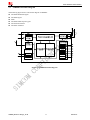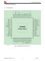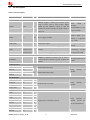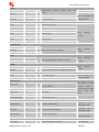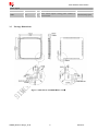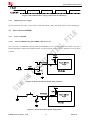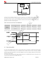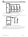
1
SIM808_Hardware Design_V1.00
Smart Machine Smart Decision
Document Title
SIM808_Hardware_Design_V1.00
Version
1.00
Date
2014-03-27
Status
Release
Document Control ID
SIM808_Hardware Design
General Notes
SIMCom offers this information as a service to its customers, to support application and engineering efforts that
use the products designed by SIMCom. The information provided is based upon requirements specifically
provided to SIMCom by the customers. SIMCom has not undertaken any independent search for additional
relevant information, including any information that may be in the customer’s possession. Furthermore, system
validation of this product designed by SIMCom within a larger electronic system remains the responsibility of the
customer or the customer’s system integrator. All specifications supplied herein are subject to change.
Copyright
This document contains proprietary technical information which is the property of SIMCom Limited, copying of
this document and giving it to others and the using or communication of the contents thereof, are forbidden
without express authority. Offenders are liable to the payment of damages. All rights reserved in the event of grant
of a patent or the registration of a utility model or design. All specification supplied herein are subject to change
without notice at any time.
Copyright © Shanghai SIMCom Wireless Solutions Ltd. 2014
SIM808_Hardware Design_V1.00
2
2014.03.27
Smart Machine Smart Decision
Contents
Contents.................................................................................................................................................................... 3
Version History ........................................................................................................................................................ 9
1
Introduction..................................................................................................................................................... 10
2
SIM808 Overview ........................................................................................................................................... 10
2.1
SIM808 Key Features............................................................................................................................. 10
2.2
Operating Modes .................................................................................................................................... 13
2.3
SIM808 Functional Diagram .................................................................................................................. 14
3
Package Information ...................................................................................................................................... 15
3.1
Pin out Diagram...................................................................................................................................... 15
3.2
Pin Description ....................................................................................................................................... 16
3.3
Package Dimensions............................................................................................................................... 18
4
GSM Application Interface ............................................................................................................................ 20
4.1
Power Supply.......................................................................................................................................... 20
4.1.1 Power Supply Pin................................................................................................................................ 21
4.1.2 Monitoring Power Supply ................................................................................................................... 22
4.2
Power on/down SIM808......................................................................................................................... 22
4.2.1 Power on SIM808 ............................................................................................................................... 22
4.2.2 Power down SIM808........................................................................................................................... 24
4.2.3 Reset Function..................................................................................................................................... 25
4.3
Power Saving Mode................................................................................................................................ 26
4.3.1 Function Mode .................................................................................................................................... 27
4.3.2 Sleep Mode (AT+CSCLK=1) ............................................................................................................. 27
4.3.3 Wake Up SIM808 from Sleep Mode (AT+CSCLK=1) ...................................................................... 27
4.4
Charging Interface .................................................................................................................................. 28
4.4.1 Battery Pack Characteristics................................................................................................................ 28
4.4.2 Recommended Battery Pack ............................................................................................................... 28
4.4.3 Implemented Charging Technique ...................................................................................................... 29
4.4.4 Operating Modes during Charging...................................................................................................... 29
4.4.5 Charger Requirements......................................................................................................................... 30
4.5
RTC Backup ........................................................................................................................................... 30
4.6
Serial Port and USB Interface ................................................................................................................ 31
4.6.1 Function of Serial Port ........................................................................................................................ 32
4.6.2 Serial Port............................................................................................................................................ 32
4.6.3 USB Interface...................................................................................................................................... 34
4.6.4 Software Upgrade and Debug ............................................................................................................. 35
4.7
RI Behaviors........................................................................................................................................... 35
4.8
Audio Interfaces ..................................................................................................................................... 36
4.8.1 Speaker Interface Configuration ......................................................................................................... 37
4.8.2 Microphone Interfaces Configuration ................................................................................................. 37
4.8.3 Audio Electronic Characteristics......................................................................................................... 38
4.8.4 TDD .................................................................................................................................................... 38
4.9
Bluetooth ................................................................................................................................................ 39
SIM808_Hardware Design_V1.00
3
2014.03.27
Smart Machine Smart Decision
4.9.1 Antenna Interface ................................................................................................................................ 39
4.10
SIM Card Interface ................................................................................................................................. 39
4.10.1
SIM Card Application...................................................................................................................... 40
4.10.2
SIM Card Design Consideration...................................................................................................... 41
4.10.3
Design Considerations for SIM Card Holder................................................................................... 41
4.11
PCM Interface ........................................................................................................................................ 43
4.11.1
PCM Multiplex Function ................................................................................................................. 43
4.11.2
PCM Interface.................................................................................................................................. 44
4.11.3
LCD Display/SPI Interface.............................................................................................................. 44
4.11.4
SD Card Interface ............................................................................................................................ 45
4.12
Keypad Interface .................................................................................................................................... 45
4.13
I2C BUS ................................................................................................................................................. 47
4.13.1
General Purpose Input/Output (GPIO) ............................................................................................ 48
4.14
ADC........................................................................................................................................................ 48
4.15
PWM ...................................................................................................................................................... 49
4.16
Network Status Indication ...................................................................................................................... 50
4.17
Operating Status Indication .................................................................................................................... 50
4.18
RF Synchronization Signal..................................................................................................................... 51
4.19
Antenna Interface ................................................................................................................................... 51
5
GPS Application Interface ............................................................................................................................. 52
5.1
GPS Operating Modes ............................................................................................................................ 52
5.2
GPS Power on/down Scenarios .............................................................................................................. 53
5.2.1 Power on GPS engine.......................................................................................................................... 53
5.2.2 Power down GPS engine..................................................................................................................... 53
5.3
GPS Antenna Interface ........................................................................................................................... 53
5.3.1 GPS Antenna Interface........................................................................................................................ 53
5.3.2 GPS Antenna Choice Consideration ................................................................................................... 53
6
Electrical, Reliability and Radio Characteristics......................................................................................... 54
6.1
Absolute Maximum Ratings................................................................................................................... 54
6.2
Recommended Operating Conditions..................................................................................................... 55
6.3
Digital Interface Characteristics ............................................................................................................. 55
6.4
SIM Card Interface Characteristics ........................................................................................................ 55
6.5
SIM_VDD Characteristics...................................................................................................................... 56
6.6
VDD_EXT Characteristics ..................................................................................................................... 56
6.7
VRTC Characteristics ............................................................................................................................. 56
6.8
Current Consumption (VBAT = 4V, GPS engine is powered down)...................................................... 56
6.9
Electro-Static Discharge ......................................................................................................................... 57
6.10
Radio Characteristics.............................................................................................................................. 58
6.10.1
Module RF Output Power................................................................................................................ 58
6.10.2
Module RF Receive Sensitivity ....................................................................................................... 59
6.10.3
Module Operating Frequencies........................................................................................................ 60
7
Manufacturing ................................................................................................................................................ 61
7.1
Top and Bottom View of SIM808........................................................................................................... 61
7.2
Typical Solder Reflow Profile ................................................................................................................ 61
7.3
The Moisture Sensitivity Level .............................................................................................................. 62
7.4
Baking Requirements ............................................................................................................................. 62
Appendix ................................................................................................................................................................ 63
SIM808_Hardware Design_V1.00
4
2014.03.27
Smart Machine Smart Decision
A. Related Documents.......................................................................................................................................... 63
B. Terms and Abbreviations ................................................................................................................................. 64
C. Safety Caution ................................................................................................................................................. 65
Table Index
TABLE 1: SIM808 GSM/GPRS ENGINE KEY FEATURES ......................................................................................... 10
TABLE 2: GPS ENGINE PERFORMANCE ................................................................................................................... 12
TABLE 3: CODING SCHEMES AND MAXIMUM NET DATA RATES OVER AIR INTERFACE ............................ 12
TABLE 4: OVERVIEW OF OPERATING MODES........................................................................................................ 13
TABLE 5: PIN DESCRIPTION ....................................................................................................................................... 16
TABLE 6: RECOMMENDED ZENER DIODE .............................................................................................................. 20
TABLE 7: ELECTRONIC CHARACTERISTIC OF THE RESET PIN.......................................................................... 26
TABLE 8: THE CURRENT CONSUMPTION OF FUNCTION MODES (BS-PA-MFRMS=5) ................................... 27
TABLE 9: SPECIFICATION OF RECOMMENDED BATTERY PACK........................................................................ 28
TABLE 10: SERIAL PORT AND USB PIN DEFINITION ............................................................................................. 31
TABLE 11: SERIAL PORT CHARACTERISTICS......................................................................................................... 31
TABLE 12: SERIAL PORT CHARACTERISTICS......................................................................................................... 34
TABLE 13: RI BEHAVIORS ........................................................................................................................................... 35
TABLE 14: AUDIO INTERFACE DEFINITION............................................................................................................ 36
TABLE 15: MICROPHONE INPUT CHARACTERISTICS........................................................................................... 38
TABLE 16: AUDIO OUTPUT CHARACTERISTICS .................................................................................................... 38
TABLE 17: SIM PIN DEFINITION................................................................................................................................. 40
TABLE 18: PIN DESCRIPTION (MOLEX SIM CARD HOLDER) .............................................................................. 42
TABLE 19: PIN DESCRIPTION (AMPHENOL SIM CARD HOLDER)....................................................................... 42
TABLE 20: PCM PIN DEFINITION ............................................................................................................................... 43
TABLE 21: PCM PIN SPECIFICATION......................................................................................................................... 43
TABLE 22: PCM MULTIPLEX FUNCTION .................................................................................................................. 43
TABLE 23: PIN DEFINITION OF THE KEYPAD INTERFACE................................................................................... 47
TABLE 24: KEYPAD MULTIPLEX FUNCTION........................................................................................................... 47
TABLE 25: PIN DEFINITION OF THE I2C ................................................................................................................... 48
TABLE 26: I2C MULTIPLEX FUNCTION .................................................................................................................... 48
TABLE 27: PIN DEFINITION OF THE GPIO................................................................................................................ 48
TABLE 28: PIN DEFINITION OF THE ADC................................................................................................................. 48
TABLE 29: ADC SPECIFICATION ................................................................................................................................ 49
TABLE 30: PIN DEFINITION OF THE PWM ............................................................................................................... 49
TABLE 31: BUZZER OUTPUT CHARACTERISTICS ................................................................................................. 49
TABLE 32: PWM MULTIPLEX FUNCTION................................................................................................................. 49
TABLE 33: PIN DEFINITION OF THE NETLIGHT ..................................................................................................... 50
TABLE 34: STATUS OF THE NETLIGHT PIN.............................................................................................................. 50
TABLE 35: PIN DEFINITION OF THE STATUS........................................................................................................... 50
TABLE 36: DEFINITION OF THE RF_SYNC PIN........................................................................................................ 51
TABLE 37: AT COMMANDS FOR GPS FUNCTION.................................................................................................... 52
TABLE 38: ABSOLUTE MAXIMUM RATINGS........................................................................................................... 54
TABLE 39: RECOMMENDED OPERATING CONDITIONS ....................................................................................... 55
TABLE 40: DIGITAL INTERFACE CHARACTERISTICS ........................................................................................... 55
TABLE 41: SIM CARD INTERFACE CHARACTERISTICS........................................................................................ 55
TABLE 42: SIM_VDD CHARACTERISTICS................................................................................................................ 56
SIM808_Hardware Design_V1.00
5
2014.03.27
Smart Machine Smart Decision
TABLE 43: VDD_EXT CHARACTERISTICS ............................................................................................................... 56
TABLE 44: VRTC CHARACTERISTICS ....................................................................................................................... 56
TABLE 45: GSM CURRENT CONSUMPTION*............................................................................................................ 56
TABLE 46: THE ESD CHARACTERISTICS (TEMPERATURE: 25℃, HUMIDITY: 45 %) ....................................... 57
TABLE 47: SIM808 GSM 900 AND GSM 850 CONDUCTED RF OUTPUT POWER ................................................ 58
TABLE 48: SIM808 DCS 1800 AND PCS 1900 CONDUCTED RF OUTPUT POWER............................................... 58
TABLE 49: SIM808 CONDUCTED RF RECEIVE SENSITIVITY ............................................................................... 59
TABLE 50: SIM808 OPERATING FREQUENCIES....................................................................................................... 60
TABLE 51: MOISTURE CLASSIFICATION LEVEL AND FLOOR LIFE ................................................................... 62
TABLE 52: BAKING REQUIREMENTS ....................................................................................................................... 62
TABLE 53: RELATED DOCUMENTS ........................................................................................................................... 63
TABLE 54: TERMS AND ABBREVIATIONS................................................................................................................ 64
TABLE 55: SAFETY CAUTION..................................................................................................................................... 65
SIM808_Hardware Design_V1.00
6
2014.03.27
Smart Machine Smart Decision
Figure Index
FIGURE 1: SIM808 FUNCTIONAL DIAGRAM ........................................................................................................... 14
FIGURE 2: SIM808 PIN OUT DIAGRAM (TOP VIEW) ............................................................................................... 15
FIGURE 3: DIMENSIONS OF SIM808(UNIT: MM)................................................................................................ 18
FIGURE 4: RECOMMENDED PCB FOOTPRINT OUTLINE(UNIT: MM)............................................................ 19
FIGURE 5: REFERENCE CIRCUIT OF THE VBAT INPUT......................................................................................... 20
FIGURE 6: REFERENCE CIRCUIT OF THE LDO POWER SUPPLY ......................................................................... 20
FIGURE 7: REFERENCE CIRCUIT OF THE DC-DC POWER SUPPLY..................................................................... 21
FIGURE 8: VBAT VOLTAGE DROP DURING TRANSMIT BURST........................................................................... 21
FIGURE 9: THE MINIMAL VBAT VOLTAGE REQUIREMENT AT VBAT DROP .................................................... 22
FIGURE 10: POWERED ON/DOWN MODULE USING TRANSISTOR..................................................................... 22
FIGURE 11: POWERED ON/DOWN MODULE USING BUTTON ............................................................................. 22
FIGURE 12: TIMING OF POWER ON MODULE......................................................................................................... 23
FIGURE 13: TIMING OF POWER ON MODULE......................................................................................................... 23
FIGURE 14: TIMING OF POWER DOWN SIM808 BY PWRKEY .............................................................................. 24
FIGURE 15: RESET CIRCUIT........................................................................................................................................ 26
FIGURE 16: RESET TIMING SEQUENCE.................................................................................................................... 26
FIGURE 17: SIM808 WITH BATTERY CHARGER AND PACK CONNECTION....................................................... 28
FIGURE 18: RTC SUPPLY FROM CAPACITOR........................................................................................................... 30
FIGURE 19: RTC SUPPLY FROM NON-CHARGEABLE BATTERY ......................................................................... 30
FIGURE 20: RTC SUPPLY FROM RECHARGEABLE BATTERY .............................................................................. 30
FIGURE 21: SEIKO XH414H-IV01E CHARGE-DISCHARGE CHARACTERISTIC ................................................. 31
FIGURE 22: CONNECTION OF THE SERIAL PORT................................................................................................... 32
FIGURE 23: LEVEL CONVERTING BY RESISTOR.................................................................................................... 33
FIGURE 24: ISOLATION CIRCUIT BY DIODES ......................................................................................................... 33
FIGURE 25: TX LEVEL CONVERTING BY TRANSISTOR........................................................................................ 33
FIGURE 26: RX LEVEL CONVERTING BY TRANSISTOR ....................................................................................... 34
FIGURE 27: USB REFERENCE CIRCUIT .................................................................................................................... 34
FIGURE 28: RI BEHAVIOUR OF VOICE CALLING AS A RECEIVER...................................................................... 35
FIGURE 29: RI BEHAVIOUR OF DATA CALLING AS A RECEIVER........................................................................ 36
FIGURE 30: RI BEHAVIOUR OF URC OR RECEIVE SMS ........................................................................................ 36
FIGURE 31: RI BEHAVIOUR AS A CALLER ............................................................................................................... 36
FIGURE 32: SPEAKER REFERENCE CIRCUIT .......................................................................................................... 37
FIGURE 33: SPEAKER WITH AMPLIFIER REFERENCE CIRCUIT ......................................................................... 37
FIGURE 34 : MICROPHONE REFERENCE CIRCUIT................................................................................................. 37
FIGURE 35: BLUETOOTH ANTENNA MATCHING CIRCUIT ................................................................................. 39
FIGURE 36: REFERENCE CIRCUIT OF THE 8-PIN SIM CARD HOLDER............................................................... 40
FIGURE 37: REFERENCE CIRCUIT OF THE 6-PIN SIM CARD HOLDER............................................................... 40
FIGURE 38: MOLEX 91228 SIM CARD HOLDER ...................................................................................................... 41
FIGURE 39: AMPHENOL C707 10M006 5122 SIM CARD HOLDER......................................................................... 42
FIGURE 40: PCM REFERENCE CIRCUIT.................................................................................................................... 44
FIGURE 41: LCD REFERENCE CIRCUIT .................................................................................................................... 44
FIGURE 42: SD REFERENCE CIRCUIT ....................................................................................................................... 45
FIGURE 43: TRADITIONAL KEYPAD REFERENCE CIRCUIT................................................................................. 45
FIGURE 44: EXTENDED KEYPAD REFERENCE CIRCUIT ...................................................................................... 46
FIGURE 45: ENHANCE THE ESD PERFORMANCE OF KEYPAD CIRCUIT........................................................... 46
FIGURE 46: KEYPAD DETECTED ............................................................................................................................... 47
FIGURE 47: REFERENCE CIRCUIT OF PWM DRIVE BUZZER ............................................................................... 49
SIM808_Hardware Design_V1.00
7
2014.03.27
Smart Machine Smart Decision
FIGURE 48: REFERENCE CIRCUIT OF NETLIGHT .................................................................................................. 50
FIGURE 49: RF_SYNC SIGNAL DURING TRANSMIT BURST ................................................................................ 51
FIGURE 50: GSM ANTENNA MATCHING CIRCUIT ................................................................................................. 51
FIGURE 51: GPS ANTENNA MATCHING CIRCUIT................................................................................................... 53
FIGURE 52: TOP AND BOTTOM VIEW OF SIM808 ................................................................................................... 61
FIGURE 53: TYPICAL SOLDER REFLOW PROFILE ................................................................................................. 61
SIM808_Hardware Design_V1.00
8
2014.03.27
Smart Machine Smart Decision
Version History
Date
Version
Description of change
Author
2014-03-27
1.00
Origin
ShengWu.Sun
Xuegang.Wang
SIM808_Hardware Design_V2.00
8
2014.03.27
Smart Machine Smart Decision
1
Introduction
This document describes SIM808 hardware interface in great detail. This document can help user to quickly
understand SIM808 interface specifications, electrical and mechanical details. With the help of this document and
other SIM808 application notes, user guide, users can use SIM808 to design various applications quickly.
2
SIM808 Overview
Designed for global market, SIM808 is integrated with a high performance GSM/GPRS engine, a GPS engine and
a BT engine. The GSM/GPRS engine is a quad-band GSM/GPRS module that works on frequencies GSM
850MHz, EGSM 900MHz, DCS 1800MHz and PCS 1900MHz. SIM808 features GPRS multi-slot class 12/ class
10 (optional) and supports the GPRS coding schemes CS-1, CS-2, CS-3 and CS-4. The GPS solution offers bestin-class acquisition and tracing sensitivity, Time-To-First-Fix (TTFF) and accuracy.
With a tiny configuration of 24*24*2.6mm, SIM808 can meet almost all the space requirements in user
applications, such as M2M, smart phone, PDA, tracker and other mobile devices.
SIM808 has 68 SMT pads, and provides all hardware interfaces between the module and customers’ boards.
z Support 4*4*2 keypads.
z One full modem serial port.
z One USB, the USB interfaces can debug, download software.
z Audio channels which include a microphone input and a receiver output.
z One SIM card interface.
z Charging interface.
z Programmable general purpose input and output.
z Support Bluetooth function.
z Support PWM and ADC.
z PCM/SPI/SD card interface, only one function can be accessed synchronously. (Default function is PCM).
SIM808 is designed with power saving technique so that the current consumption is as low as 1mA in sleep mode
(GPS engine is powered down).
SIM808 integrates TCP/IP protocol and extended TCP/IP AT commands which are very useful for data transfer
applications. For details about TCP/IP applications, please refer to document [2].
2.1
SIM808 Key Features
Table 1: SIM808 GSM/GPRS engine key features
Feature
Implementation
Power supply
3.4V ~ 4.4V
Power saving
Typical power consumption in sleep mode is 1mA ( BS-PA-MFRMS=9, GPS
engine is powered down )
Charging
Supports charging control for Li-Ion battery
Frequency bands
z
SIM808_Hardware Design_V1.00
SIM808 Quad-band: GSM 850, EGSM 900, DCS 1800, PCS 1900. SIM808
10
2014.03.27
Smart Machine Smart Decision
z
can search the 4 frequency bands automatically. The frequency bands also
can be set by AT command “AT+CBAND”. For details, please refer to
document [1].
Compliant to GSM Phase 2/2+
Transmitting power
z
z
Class 4 (2W) at GSM 850 and EGSM 900
Class 1 (1W) at DCS 1800 and PCS 1900
GPRS connectivity
z
z
GPRS multi-slot class 12(default)
GPRS multi-slot class 1~12 (optional)
Temperature range
z
z
Normal operation: -40℃ ~ +85℃
Storage temperature -45℃~ +90℃
Data GPRS
z
z
z
z
z
z
z
GPRS data downlink transfer: max. 85.6 kbps
GPRS data uplink transfer: max. 85.6 kbps
Coding scheme: CS-1, CS-2, CS-3 and CS-4
PAP protocol for PPP connect
Integrate the TCP/IP protocol.
Support Packet Broadcast Control Channel (PBCCH)
CSD transmission rates:2.4,4.8,9.6,14.4 kbps
CSD
z
Support CSD transmission
USSD
z
Unstructured Supplementary Services Data (USSD) support
SMS
z
z
MT, MO, CB, Text and PDU mode
SMS storage: SIM card
SIM interface
Support SIM card: 1.8V, 3V
External antenna
Antenna pad
Audio features
Speech codec modes:
z Half Rate (ETS 06.20)
z Full Rate (ETS 06.10)
z Enhanced Full Rate (ETS 06.50 / 06.60 / 06.80)
z Adaptive multi rate (AMR)
z Echo Cancellation
z Noise Suppression
z
Serial port and
USB interface
z
z
z
z
z
z
Serial port:
Full modem interface with status and control lines, unbalanced,
asynchronous.
1200bps to 115200bps.
Can be used for AT commands or data stream.
Support RTS/CTS hardware handshake and software ON/OFF flow control.
Multiplex ability according to GSM 07.10 Multiplexer Protocol.
Autobauding supports baud rate from 1200 bps to 115200bps.
USB interface:
Can be used as debugging and firmware upgrading.
Phonebook management
Support phonebook types: SM, FD, LD, RC, ON, MC.
SIM application toolkit
GSM 11.14 Release 99
Real time clock
Support RTC
Alarm function
Can be set by AT command
Physical characteristics
Size: 24*24*2.6mm
Weight: 3.5g
SIM808_Hardware Design_V1.00
11
2014.03.27
Smart Machine Smart Decision
Firmware upgrade
Firmware upgrading by USB interface.
Table 2: GPS engine Performance
Performance
Parameter
Description
Horizontal Position
Accuracy(1)
Autonomous
<2.5
m
Velocity
Accuracy(2)
Without Aid
0.1
m/s
DGPS
0.05
m/s
Acceleration
Accuracy
Without Aid
0.1
m/s2
DGPS
0.05
m/s2
10
nS
Min
Timing Accuracy
Dynamic
Performance
Time To First Fix(3)
Sensitivity
Receiver
Type
Max
Unit
Maximum Altitude
18000
m
Maximum Velocity
515
m/s
Maximum Acceleration
4
G
Hot start
1
s
Warm start
28
s
Cold start
30
s
Autonomous
acquisition(cold start)
-147
dBm
Re-acquisition
-159
dBm
Tracking
-165
dBm
Channels
22/66
Update rate
5
Hz
Tracking L1, CA Code
Protocol support NMEA
Power
consumption(4)
Acquisition
42
mA
Continuous tracking
24
mA
(1) 50% 24hr static, -130dBm
(2) 50% at 30m/s
(3) GPS signal level: -130dBm
(4) Single Power supply 3.8V@-130dBm,GSM IDLE
Table 3: Coding schemes and maximum net data rates over air interface
Coding scheme
1 timeslot
2 timeslot
4 timeslot
CS-1
9.05kbps
18.1kbps
36.2kbps
CS-2
13.4kbps
26.8kbps
53.6kbps
CS-3
15.6kbps
31.2kbps
62.4kbps
CS-4
21.4kbps
42.8kbps
85.6kbps
SIM808_Hardware Design_V1.00
12
2014.03.27
Smart Machine Smart Decision
2.2
Operating Modes
The table below summarizes the various operating modes of SIM808.
Table 4: Overview of operating modes
Mode
Normal
operation
Function
GSM/GPRS
SLEEP
Module will automatically go into sleep mode if the conditions of sleep
mode are enabling and there is no on air and no hardware interrupt (such as
GPIO interrupt or data on serial port).
In this case, the current consumption of module will reduce to the minimal
level.
In sleep mode, the module can still receive paging message and SMS.
GSM
IDLE
Software is active. Module registered to the GSM network, and the module
is ready to communicate.
GSM
TALK
Connection between two subscribers is in progress. In this case, the power
consumption depends on network settings such as DTX off/on,
FR/EFR/HR, hopping sequences, antenna.
GPRS
STANDBY
Module is ready for GPRS data transfer, but no data is currently sent or
received. In this case, power consumption depends on network settings and
GPRS configuration.
GPRS
DATA
There is GPRS data transfer (PPP or TCP or UDP) in progress. In this case,
power consumption is related with network settings (e.g. power control
level); uplink/downlink data rates and GPRS configuration (e.g. used
multi-slot settings).
Charge
The mode support charge function (Default is not support).
Power down
Normal power down by sending the AT command “AT+CPOWD=1” or using the PWRKEY.
The power management unit shuts down the power supply for the baseband part of the
module, and only the power supply for the RTC is remained. Software is not active. The
serial port is not accessible. Power supply (connected to VBAT) remains applied.
Minimum
functionality
mode
AT command “AT+CFUN” can be used to set the module to a minimum functionality mode
without removing the power supply. In this mode, the RF part of the module will not work or
the SIM card will not be accessible, or both RF part and SIM card will be closed, and the
serial port is still accessible. The power consumption in this mode is lower than normal
mode.
SIM808_Hardware Design_V1.00
13
2014.03.27
Smart Machine Smart Decision
2.3
SIM808 Functional Diagram
The following figure shows a functional diagram of SIM808:
z The GSM baseband engine
z The GPS engine
z Flash
z The GSM radio frequency part
z The antenna interface
z The other interfaces
Figure 1: SIM808 functional diagram
SIM808_Hardware Design_V1.00
14
2014.03.27
Smart Machine Smart Decision
3
3.1
Package Information
Pin out Diagram
Figure 2: SIM808 pin out diagram (Top view)
SIM808_Hardware Design_V1.00
15
2014.03.27
Smart Machine Smart Decision
3.2
Pin Description
Table 5: Pin description
Pin name
Pin number
I/O
Description
Comment
I
SIM808 supplies 3 VBAT pins, and the power
range is from 3.4V to 4.4V. Power supply
should provide sufficient current so that the
module can work normally; the peak current is
nearly 2A.
Zener
diode
is
Strongly
recommended to anti
surge on VBAT.
Power supply
VBAT
4,5,6
VRTC
17
I/O
Power supply for RTC
It is recommended to
connect VRTC to a
battery or a capacitor
(e.g. 4.7uF).
VDD_EXT
7
O
2.8V power output
Keep
floating
unused.
GND
1,2,3,18,28,34
,36,40,51,52,5
4,64,65,67,68
if
Recommend
connecting 1,2,3pin
to the power GND.
Ground
Power on/off
PWRKEY
8
I
PWRKEY should be pulled low at least 1
second and then released to power on/down the
module.
I
Differential audio input
O
Differential audio output
Internally pulled up to
VBAT.
Audio interface
MIC1P
19
MIC1N
20
SPK1P
21
SPK1N
22
Keep
floating
unused.
if
PCM interface for audio
Keep
floating
unused.
if
Support up to 32 buttons (4*4*2)
Keep
floating
if
unused. (COL0 can
not be pulled down).
PCM interface
PCM_OUT
48
O
PCM_IN
47
I
PCM_SYNC
45
O
PCM_CLK
46
I
COL3
59
I
COL2
60
I
COL1
61
I
COL0
62
I
ROW3
55
O
ROW2
56
O
ROW1
57
O
ROW0
58
O
Keypad interface
SIM808_Hardware Design_V1.00
16
2014.03.27
Smart Machine Smart Decision
GPIO
GPIO5
43
I/O
GPIO6
44
I/O
Programmable
output.
general
NETLIGHT
50
O
Network status
STATUS
49
O
Power on status
DTR
9
I
Data terminal ready
RI
10
O
Ring indicator
DCD
11
O
Data carrier detect
CTS
12
O
Clear to send
RTS
13
I
Request to send
TXD
14
O
Transmit data
RXD
15
I
Receive data
VBUS
25
I
USB_DP
26
I/O
USB_DM
27
I/O
purpose
input
and
Can not multiplex with
GPIO function.
Serial port
Keep
floating
unused.
if
Debug and firmware upgrading
Keep
floating
unused.
if
I
10 bit general analog to digital converter
Keep
floating
unused.
if
Keep
floating
unused.
if
USB interface
ADC
ADC1
23
ADC2
24
PWM
PWM1
42
O
Pulse-width modulation, multiplex with GPIO4.
PWM2
41
O
Pulse-width modulation, multiplex with GPIO3.
SDA
38
I/O
I2C serial bus data
SCL
39
O
I2C serial bus clock
SIM_VDD
29
O
Voltage supply for SIM card. Support 1.8V or
3V for SIM card
SIM_DATA
30
I/O
SIM data input/output
SIM_CLK
31
O
SIM clock
SIM_RST
32
O
SIM reset
SIM_PRESENCE
33
I
SIM card detection
GSM_RF_IN
66
I/O
Connect GSM antenna
Impendence must be
controlled to 50Ω.
ANT_BT
53
I/O
Connect Bluetooth antenna
Impendence must be
controlled to 50Ω.
GPS_RF_IN
35
I
Connect GPS antenna
Impendence must be
controlled to 50Ω.
63
O
RF burst synchronous signal
Do not pull up
I2C
Internal pulled up to
2.8V via 4.7KΩ
SIM interface
All signals of SIM
interface should be
protected against ESD
with a TVS diode
array.
Antenna
RF synchronization
RF_SYNC
SIM808_Hardware Design_V1.00
17
2014.03.27
Smart Machine Smart Decision
Other signal
RESET
16
I
Reset input(Active low)
1PPS
37
I
Time Mark outputs timing pulse related to
receiver time
3.3
If unused, keep open.
Package Dimensions
Figure 3: Dimensions of SIM808(Unit: mm)
SIM808_Hardware Design_V1.00
18
2014.03.27
Smart Machine Smart Decision
Figure 4: Recommended PCB footprint outline(Unit: mm)
SIM808_Hardware Design_V1.00
19
2014.03.27
Smart Machine Smart Decision
4
4.1
GSM Application Interface
Power Supply
The power supply range of SIM808 is from 3.4V to 4.4V.Recommended voltage is 4.0V.The transmitting burst
will cause voltage drop and the power supply must be able to provide sufficient current up to 2A. For the VBAT
input, a bypass capacitor (low ESR) such as a 100 µF is strongly recommended.
Increase the 33PF and 10PF capacitors can effectively eliminate the high frequency interference. A 5.1V/500mW
Zener diode is strongly recommended, the diode can prevent chip from damaging by the voltage surge. These
capacitors and Zener diode should be placed as close as possible to SIM808 VBAT pins.
Figure 5: Reference circuit of the VBAT input
Table 6: Recommended Zener diode
Vendor
Part number
Power(watts)
Packages
1
On semi
MMSZ5231BT1G
500mW
SOD123
2
Prisemi
PZ3D4V2H
500mW
SOD323
3
Prisemi
PZ5D4V2H
500mW
SOD523
4
Vishay
MMSZ4689-V
500mW
SOD123
5
Crownpo
CDZ55C5V1SM
500mW
0805
The following figure is the reference design of +5V input power supply. The designed output for the power
supply is 4.1V, thus a linear regulator can be used.
Figure 6: Reference circuit of the LDO power supply
SIM808_Hardware Design_V1.00
20
2014.03.27
Smart Machine Smart Decision
If there is a high drop-out between the input and the desired output (VBAT), a DC-DC power supply will be
preferable because of its better efficiency especially with the 2A peak current in burst mode of the module. The
following figure is the reference circuit.
Figure 7: Reference circuit of the DC-DC power supply
The single 3.7V Li-ion cell battery can be connected to SIM808 VBAT pins directly. But the Ni-Cd or Ni-MH
battery must be used carefully, since their maximum voltage can rise over the absolute maximum voltage of the
module and damage it.
Notes:The module do not support for charging Ni-Cd or Ni-MH battery.
When battery is used, the total impedance between battery and VBAT pins should be less than 150mΩ.
The following figure shows the VBAT voltage drop at the maximum power transmit phase, and the test condition
is as following:
VBAT=4.0V,
A VBAT bypass capacitor CA=100µF tantalum capacitor (ESR=0.7Ω),
Another VBAT bypass capacitor CB=1µF.
Figure 8: VBAT voltage drop during transmit burst
4.1.1
Power Supply Pin
The 3 VBAT pins are used for power input, and pin 4, 5, 6 should be connected to the power GND. VRTC pin is
power supply of the RTC circuit in the module. VDD_EXT will output 2.8V when module powered up.
When designing the power supply in user’s application, pay special attention to power losses. Ensure that the
input voltage never drop below 3.0V even when current consumption rises to 2A in the transmit burst. If the
power voltage drops below 3.0V, the module may be shut down automatically. The PCB traces from the VBAT
pins to the power supply must be wide enough (at least 60mil) to decrease voltage drops in the transmit burst. The
power IC and the bypass capacitor should be placed to the module as close as possible.
SIM808_Hardware Design_V1.00
21
2014.03.27
Smart Machine Smart Decision
Figure 9: The minimal VBAT voltage requirement at VBAT drop
4.1.2
Monitoring Power Supply
The AT command “AT+CBC” can be used to monitor the VBAT voltage. For detail, please refer to document [1].
4.2
Power on/down SIM808
4.2.1
4.2.1.1
Power on SIM808
Turn on SIM808 Using the PWRKEY Pin (Power on)
User can power on SIM808 by pulling down the PWRKEY pin for at least 1 second and release. This pin is
already pulled up to VBAT in the module internal, so external pull up is not necessary. Reference circuit is shown
as below.
Figure 10: Powered on/down module using transistor
Figure 11: Powered on/down module using button
SIM808_Hardware Design_V1.00
22
2014.03.27
Smart Machine Smart Decision
The power on scenarios is illustrated as following figure.
Figure 12: Timing of power on module
When power on procedure is completed, SIM808 will send following URC to indicate that the module is ready to
operate at fixed baud rate.
RDY
This URC does not appear when autobauding function is active.
Note: User can use AT command “AT+IPR=x” to set a fixed baud rate and save the configuration to non-volatile flash memory.
After the configuration is saved as fixed baud rate, the Code “RDY” should be received from the serial port every time when
SIM808 is powered on. For details, please refer to the chapter “AT+IPR” in document [1].
4.2.1.2
Turn on the SIM808 using the VBUS Signal
The SIM808 will be automatically turned on when a charger is connected to VBUS pin, the switched-off
SIM808 of which VBAT pin voltage is greater than 3.4V. SIM808 will power up.
Figure 13: Timing of power on module
SIM808_Hardware Design_V1.00
23
2014.03.27
Smart Machine Smart Decision
4.2.2
Power down SIM808
SIM808 will be powered down in the following situations:
z Normal power down procedure: power down SIM808 by the PWRKEY pin.
z Normal power down procedure: power down SIM808 by AT command “AT+CPOWD=1”.
z Abnormal power down: over-voltage or under-voltage automatic power down.
z Abnormal power down: over-temperature or under-temperature automatic power down.
NOTE:The VBUS pin should not be charged, otherwise ,the module will not be powered down.
4.2.2.1
Power down SIM808 by the PWRKEY Pin
User can power down SIM808 by pulling down the PWRKEY pin for at least 1 second and release. Please refer to
the power on circuit. The power down scenario is illustrated in following figure.
Figure 14: Timing of power down SIM808 by PWRKEY
This procedure makes the module log off from the network and allows the software to enter into a secure state to
save data before completely shut down.
Before the completion of the power down procedure, the module will send URC:
NORMAL POWER DOWN
At this moment, AT commands can not be executed any more, and only the RTC is still active. Power down mode
can also be indicated by STATUS pin, which is at low level at this time.
4.2.2.2
Power down SIM808 by AT Command
SIM808 can be powered down by AT command “AT+CPOWD=1”. This procedure makes the module log off
from the network and allows the software to enter into a secure state to save data before completely shut down.
Before the completion of the power down procedure, the module will send URC:
NORMAL POWER DOWN
At this moment, AT commands can not be executed any more, and only the RTC is still active. Power down mode
can also be indicated by STATUS pin, which is at low level at this time.
SIM808_Hardware Design_V1.00
24
2014.03.27
Smart Machine Smart Decision
For detail about the AT command “AT+CPOWD”, please refer to document [1]
4.2.2.3
Over-voltage or Under-voltage Power down
The module software monitors the VBAT voltage constantly.
If the voltage ≤ 3.5V, the following URC will be reported:
UNDER-VOLTAGE WARNNING
If the voltage ≥ 4.3V, the following URC will be reported:
OVER-VOLTAGE WARNNING
If the voltage < 3.4V, the following URC will be reported, and the module will be automatically powered down.
UNDER-VOLTAGE POWER DOWN
If the voltage > 4.4V, the following URC will be reported, and the module will be automatically powered down.
OVER-VOLTAGE POWER DOWN
At this moment, AT commands can not be executed any more, and only the RTC is still active. Power down mode
can also be indicated by STATUS pin, which is at low level at this time.
4.2.2.4
Over-temperature or Under-temperature Power down
The module will constantly monitor the temperature of the module,
If the temperature > +80℃, the following URC will be reported:
+CMTE: 1
If the temperature < -30℃, the following URC will be reported:
+CMTE:-1
If the temperature > +85℃, the following URC will be reported, and the module will be automatically powered
down.
+CMTE: 2
If the temperature < -40℃, the following URC will be reported, and the module will be automatically powered
down.
+CMTE:-2
At this moment, AT commands can not be executed any more, and only the RTC is still active. Power down mode
can also be indicated by STATUS pin, which is at low level at this time.
The AT command “AT+CMTE” could be used to read the temperature when the module is running.
For details please refer to document [1].
4.2.3
Reset Function
SIM808 also has a RESET pin (pin 16) used to reset the module. This function is used as an emergency reset
only when AT command “AT+CPOWD=1” and the POWER_ON pin has no effect. User can pull the RESET pin
to ground, then the module will reset.
This pin is already isolated in the module, so the external isolation is not necessary. Following figure is internal
circuit of the RESET pin.
SIM808_Hardware Design_V1.00
25
2014.03.27
Smart Machine Smart Decision
Figure 15: Reset Circuit
The typical value of RESET pin high level is 2.8V, so for the 3V or 3.3V, customer could use MCU’s GPIO to
driver this pin directly, resistor in serial the RESET signal could enhance the ESD performance but the value
should not be too high, otherwise the level of RESET could be lower than threshold value; RESET hardware
parameters can refer to the following table.
Table 7: Electronic characteristic of the RESET Pin
Pin name
RESET
Symbol
Min
Typ
Max
Unit
VIH
2.7
2.8
2.9
V
VIL
-
-
0.6
V
-
mS
Tpull down
105
The reset scenarios are illustrated in the following figures.
Figure 16: Reset timing sequence
4.3
Power Saving Mode
User can control SIM808 module to enter or exit the sleep mode (AT+CSCLK=1) by DTR signal. When DTR is
in high level and without interrupt (on air and hardware such as GPIO interrupt or data in serial port), SIM808
will enter sleep mode automatically. In this mode, SIM808 can still receive paging or SMS from network but the
serial port is not accessible.
Note: Customer must shut off the power supply of GPS, and then the AT commands about the power saving mode can be
executed correctly, and the current consumption will be lower.
SIM808_Hardware Design_V1.00
26
2014.03.27
Smart Machine Smart Decision
4.3.1
Function Mode
There are three functionality modes, which could be set by the AT command “AT+CFUN=<fun>”. The command
provides the choice of the functionality levels <fun>=0, 1, 4.
z AT+CFUN=0: minimum functionality.
z AT+CFUN=1: full functionality (default).
z AT+CFUN=4: flight mode (disable RF function).
Table 8: The current consumption of function modes (BS-PA-MFRMS=5)
<Fun>
Current consumption(uA) (CSCLK=1)
0
869.5
1
1400
4
922.5
Minimum functionality mode minimizes the current consumption to the lowest level. If SIM808 is set to
minimum functionality by “AT+CFUN=0”, the RF function and SIM card function will be disabled. In this case,
the serial port is still accessible, but all AT commands correlative with RF function and SIM card function will not
be accessible.
For detailed information about the AT Command “AT+CFUN=<fun>”, please refer to document [1].
4.3.2
Sleep Mode (AT+CSCLK=1)
When the GPS function is shut off, user can control SIM808 module to enter or exit the sleep mode
(AT+CSCLK=1) by DTR signal. When DTR is in high level and without interrupt (on air and hardware such as
GPIO interrupt or data in serial port), SIM808 will enter sleep mode automatically. In this mode, SIM808 can still
receive paging or SMS from network but the serial port is not accessible.
Note: For SIM808, it requests to set AT command “AT+CSCLK=1” and ensure DTR at high level to enable the sleep mode ; the
default value is 0, which can not make the module to enter sleep mode. For more details please refer to document [1].
4.3.3
Wake Up SIM808 from Sleep Mode (AT+CSCLK=1)
When SIM808 is in sleep mode (AT+CSCLK=1), the following methods can wake up the module:
z Pull down DTR pin.
The serial port will be active after DTR pin is pulled to low level for about 50ms.
z Receive a voice or data call from network.
z Receive a SMS from network.
z Receive external interrupt
z Charge VBUS pin
SIM808_Hardware Design_V1.00
27
2014.03.27
Smart Machine Smart Decision
4.4
Charging Interface
SIM808 has integrated a charging circuit inside the module for Li-Ion batteries charging control, which make it
very convenient for user’s applications that support battery charging. A common connection is shown in the
following figure:
5V
VBUS
VBAT
M o d u le
B a tte ry
P a ck
Figure 17: SIM808 with battery charger and pack connection
4.4.1
Battery Pack Characteristics
SIM808 has optimized the charging algorithm for the Li-Ion battery that meets the characteristics listed below.
z The maximum charging voltage of the Li-Ion battery pack is 4.2V and the recommended capacity is
1100mAh. The Battery packs with more than 1100 mAh capacity will take more time for charging.
z The battery pack should have a protection circuit to avoid overcharging, deep discharging and over-current,
and the circuit should be insensitive to pulsed current.
z The internal resistance of the battery pack including protection circuit should be as low as possible. Its
recommended value does not exceed 150mΩ.
z The battery pack must be protected from reverse pole connection.
On the SIM808, the build-in circuit of the power management chipset monitors the supply voltage constantly.
Once the Under-voltage is detected, the SIM808 will be powered down automatically.
4.4.2
Recommended Battery Pack
Following is the specification of recommended battery pack:
Table 9: Specification of recommended battery pack
Items
Description
Battery type
Li-ion
Manufacturer
Jiade Energy Technology
Normal voltage
3.7V
Capacity
NORMAL 1100mAh
Charge Voltage
4.200±0.050V
SIM808_Hardware Design_V1.00
28
2014.03.27
Smart Machine Smart Decision
Max Charge Current
1.0C
Charge Method
CC / CV (Constant Current / Constant Voltage)
Max Discharge Current
1.0C (for continuous discharging mode)
Discharge Cut-off Voltage
3.0V/ cell
Internal resistance
Initial≤150mΩ
4.4.3
Implemented Charging Technique
SIM808 has battery charging function, but default function is not support for charging, the customer should input
AT command to enable charging function. There are two pins related to the battery charging function: there are
VBUS, VBAT and pins. The VBUS Pin is driven by an external voltage (AC adapter or USB host), system can
use this Pin to detect a charger supply and provide most charging current through SIM808 module to battery when
charging is in fast charge state. VBAT pin gives charging current to external battery from SIM808 module.
It is very simple to implement charging function, user just needs to connect the charger to the VBUS Pin and
connect the battery to the VBAT Pin.
SIM808 battery charging happens after detecting charger supply and the presence of battery. If there is no charger
supply or no battery present, charging function will not be enabled.
Normally, there are three states in the whole charging procedure.
z DDLO charge (Pull-up mode) and UVLO charge (Pre-charge mode);
z Constant current mode (CC);
z Constant voltage mode and over-voltage protection(OV)
DDLO charge and UVLO charge:
DDLO is the state of battery when its voltage is under 2.2V. And UVLO means the battery voltage is less than
3.3V and more than 2.2V. The battery is not suitable for fast charging when its condition is DDLO or UVLO. The
SIM808 provides a small constant current to the battery when the battery is between DDLO and UVLO. In DDLO
charging state, SIM808 gives out pu1se 70mA current to the battery. And in UVLO charging state, SIM808
provides about 200mA (AC<7V) or 70mA (USB mode) current to the battery.
DDLO charging terminates when the battery voltage reaches 2.2V. UVLO charging terminates when the battery
voltage is up to 3.4V. Both DDLO and UVLO charge are controlled by the SIM808 hardware only.
Constant current mode (CC):
As the battery voltage is charged up and over3.4V, the SIM808 will enter CC mode. The CC mode charging
current can be set from 70 to 800mA by the software.
Constant voltage mode (CV) and over-voltage protection (OV):
As the battery is charged up and over 4.05V, the SIM808 will enter CV mode. While the batter voltage actually
reaches 4.2V, the charging current is gradually decreased step by step until stop charging.
4.4.4
Operating Modes during Charging
The battery can be charged during various operating mode. That means that charging can be in progress while
SIM808 is in Normal mode (SLEEP, IDLE, TALK, GPRS IDLE or GPRS DATA mode). In this case the voltage
supply should be sufficient. Here Charging in Normal mode is named as Charge mode.
If the charger is connected to the module’s VBUS Pin and the valid battery is connected to the VBAT Pin while
SIM808 is in POWER DOWN mode, SIM808 will auto power up.
SIM808_Hardware Design_V1.00
29
2014.03.27
Smart Machine Smart Decision
4.4.5
Charger Requirements
Following is the requirements of charger for SIM808:
z Simple transformer power plug
z Output voltage: 5.0V~7V
z Minimum supply current: 800mA
z A 10V peak voltage is allowed for maximum 1ms when charging current is switched off.
z A 1.6A peak current is allowed for maximum 1ms when charging current is switched on.
4.5
RTC Backup
Current input for RTC when the VBAT is not supplied for the system. Current output for backup battery when
the VBAT power supply is in present and the backup battery is in low voltage state. The RTC power supply of
module can be provided by an external capacitor or a battery (non-chargeable or rechargeable) through the VRTC.
The following figures show various reference circuits for RTC back up.
z
External capacitor for RTC
Figure 18: RTC supply from capacitor
z
Non-chargeable battery for RTC
Figure 19: RTC supply from non-chargeable battery
z
Rechargeable battery for RTC
Figure 20: RTC supply from rechargeable battery
SIM808_Hardware Design_V1.00
30
2014.03.27
Smart Machine Smart Decision
Coin-type rechargeable battery is recommended, such as XH414H-IV01E from Seiko can be used.
Typical charge-discharge curves for this battery are shown in the following figure.
Figure 21: Seiko XH414H-IV01E charge-discharge characteristic
4.6
Serial Port and USB Interface
SIM808 provides one unbalanced asynchronous serial port. The module is designed as a DCE (Data
Communication Equipment). The following figure shows the connection between module and client (DTE).
Table 10: Serial port and USB pin definition
Serial port
USB
interface
Name
Pin number
Function
DTR
9
Data terminal ready
RI
10
Ring indicator
DCD
11
Data carrier detect
CTS
12
Clear to send
RTS
13
Request to send
TXD
14
Transmit data
RXD
15
Receive data
VBUS
25
USB power supply
USB_DP
26
USB data line plus
USB_DM
27
USB data line minus
Note: Hardware flow control is disabled by default. The AT command “AT+IFC=2,2” can enable hardware flow control .The AT
command “AT+IFC=0,0”can disable hardware flow control. For more details, please refer to document [1].
Table 11: Serial port characteristics
Symbol
Min
Max
Unit
VIL
0
0.3
V
VIH
2.5
2.8
V
VOL
0
0.1
V
VOH
2.7
2.8
V
SIM808_Hardware Design_V1.00
31
2014.03.27
Smart Machine Smart Decision
4.6.1
Function of Serial Port
Serial port:
z Full modem device.
z Contains data lines TXD and RXD, hardware flow control lines RTS and CTS, status lines DTR, DCD and
RI.
z Serial port can be used for CSD FAX, GPRS service and AT communication..
z Serial port supports the following baud rates:
1200, 2400, 4800, 9600, 19200, 38400, 57600 and 115200bps
z Autobauding only supports the following baud rates:
1200, 2400, 4800, 9600, 19200, 38400, 57600 and 115200bps
z The default setting is autobauding.
Autobauding allows SIM808 to automatically detect the baud rate of the host device. Pay more attention to the
following requirements:
z Synchronization between DTE and DCE:
When DCE powers on with autobauding enabled, firstly, user must send character “A” or “a” to
synchronize the baud rate. It is recommended to send “AT” until DTE receives the “OK” response, which
means DTE and DCE are correctly synchronized. For more information please refer to the AT command
“AT+IPR”.
z
Restrictions of autobauding operation:
The DTE serial port must be set at 8 data bits, no parity and 1 stop bit.
The URC such as "RDY", "+CFUN: 1" and "+CPIN: READY” will not be reported.
Note: User can use AT command “AT+IPR=x” to set a fixed baud rate and the setting will be saved to non-volatile flash memory
automatically. After the configuration is set as fixed baud rate, the URC such as "RDY", "+CFUN: 1" and "+CPIN: READY”
will be reported when SIM808 is powered on.
4.6.2
Serial Port
The following figure shows the connection between module and client (DTE).
Figure 22: Connection of the serial port
If the voltage of UART is 3.3V, the following reference circuits are recommended. If the voltage is 3.0V, please
SIM808_Hardware Design_V1.00
32
2014.03.27
Smart Machine Smart Decision
change the resistors in the following figure from 5.6K to 14K.
Figure 23: Level converting by resistor
If the voltage of UART is 3V or3.3V, user also can use following reference circuits:
Figure 24: Isolation circuit by diodes
Note: when a diode used to isolate voltage cross, customer should notice that there’s voltage drop on the diode. And the
signal’s voltage level should meet the customer’s electrical character. The recommend diode is Schottky diode e.g.
RB551V-30TE-17 and SDM20U40.
If the voltage of UART is 5V on customer side, customer can use the following reference circuits :
Figure 25: TX level converting by transistor
SIM808_Hardware Design_V1.00
33
2014.03.27
Smart Machine Smart Decision
VDD_EXT
Customer
VDD_EXT
MCUVDD
4.7K
4.7K
Module
47K
MCUTXD
RXD
Figure 26: RX level converting by transistor
Note: The recommend Transistors’ part numbers are 2SC4617TLR and PBHV8115Z. when update firmware via the TXD/RXD
circuit as figure 25 and figure 26 shows, customer should make sure the VDD_EXT has voltage output, or a external LDO should
be added to power VDD_EXT.
4.6.3
USB Interface
USB interface supports software debug function. When power on the module, connect VBUS, USB_DP,
USB_DM and GND to PC, then install the driver successfully, a UART port could be recognized by the PC,
customer could achieve the software Debug purpose with this UART port.
The following diagram is recommended:
Figure 27: USB reference circuit
The maximum allowable cap load of TVS on USB data line should be less than 5pF (e.g. ESD9L5.0ST5G and
ESD9M5.0ST5G). The USB_DP and USB_DM should be routed in differential traces.
Note: please reserve the USB interface or test point for debug.
Table 12: Serial port characteristics
Pin
Min
Typ
Max
Unit
VBUS
4.3
5
7
V
SIM808_Hardware Design_V1.00
34
2014.03.27
Smart Machine Smart Decision
4.6.4
Software Upgrade and Debug
Only USB and interface can be used for firmware upgrade.
If customer upgrading firmware via the USB port, SIM808 must be powered first, then connect VBUS, USB_DP,
USB_DM and GND to PC. There is no need to operate PWRKEY pin in the whole procedure, when SIM808
detects VBUS and could communicate normally by USB_DP and USB_DM, module will enter USB download
mode automatically.
Note: When only USB_DP and USB_DM connected, no VBUS, customer need to pull down COL0 before power on the module,
then press the PWRKEY button, the module will enter download mode;
The serial port and the debug port support the CMOS level. If user connects the module to the computer, the
level shifter should be added between the DCE and DTE.
For details about software upgrading, please refer to document [4].
4.7
RI Behaviors
Table 13: RI Behaviors
State
RI response
Standby
High
Voice call
The pin is changed to low. When any of the following events occur, the pin will be
changed to high:
(1)Establish the call
(2)Hang up the call
Data call
The pin is changed to low. When any of the following events occur, the pin will be
changed to high:
(1)Establish the call
(2)Hang up the call
SMS
The pin is changed to low, and kept low for 120ms when a SMS is received. Then it is
changed to high.
URC
The pin is changed to low, and kept low for 120ms when some URCs are reported. Then it
is changed to high. For more details, please refer to document [10].
The behavior of the RI pin is shown in the following figure when the module is used as a receiver.
Figure 28: RI behaviour of voice calling as a receiver
SIM808_Hardware Design_V1.00
35
2014.03.27
Smart Machine Smart Decision
Figure 29: RI behaviour of data calling as a receiver
Figure 30: RI behaviour of URC or receive SMS
However, if the module is used as caller, the RI will remain high. Please refer to the following figure.
RI
HIGH
LOW
Idle
Ring
Establish
the call
Hang up
the call
Idle
Figure 31: RI behaviour as a caller
4.8
Audio Interfaces
SIM808 provides one analog input, which could be used for electret microphone. The module also provides one
analog output. The output can directly drive 32Ω receiver.
Table 14: Audio interface definition
Audio
channel
Pin name
Pin number
Function
MIC1P
19
Main Audio input positive
MIC1N
20
Main Audio input negative
SPK1P
21
Main Audio output positive
SPK1N
22
Main Audio output negative
“AT+CMIC” is used to adjust the input gain level of microphone. “AT+SIDET” is used to set the side-tone
level. In addition, “AT+CLVL” is used to adjust the output gain level. For more details, please refer to
document [1]
SIM808_Hardware Design_V1.00
36
2014.03.27
Smart Machine Smart Decision
In order to improve audio performance, the following reference circuits are recommended. The audio signals have
to be layout according to differential signal layout rules as shown in following figures.
4.8.1
Speaker Interface Configuration
These components should
be placed to speaker as
close as possible
The lines in bold type should
be accorded to differential
signal layout rules
10pF
33pF
10pF
33pF
10pF
33pF
ESD
ANTI
SPK1P
MODULE
SPK1N
ESD
ANTI
Figure 32: Speaker reference circuit
Figure 33: Speaker with amplifier reference circuit
4.8.2
Microphone Interfaces Configuration
Figure 34 : Microphone reference circuit
SIM808_Hardware Design_V1.00
37
2014.03.27
Smart Machine Smart Decision
4.8.3
Audio Electronic Characteristics
Table 15: Microphone input characteristics
Parameter
Min
Mic biasing voltage
Typ
Max
Unit
1.9
2.2
V
2
mA
27
KΩ
-67
dBm
Working Current
Input impedance(differential)
13
20
Idle channel noise
SINAD
Input level:-40dBm0
29
dB
Input level:0dBm0
69
dB
Table 16: Audio output characteristics
parameter
Conditions
Min
Typ
Max
Unit
Normal output
RL=32 Ω receiver
-
90
-
mW
4.8.4
TDD
GSM signal could interfere audio by coupling or conducting. Coupling noise could be filtered by adding 33 pF
and 10pF capacitor over audio lines.33pF capacitor could eliminate noise from GSM900MHz, while 10pF
capacitor could eliminate noise from DCS1800MHz frequency. Coupling noise has great relatives with PCB
layout. Under some scenarios, TDD noise from GSM 900MHz frequency affects heavily, but some different
story is from GSM1800MHz fervency, so customer should develop this filter solution according to field test
result.
GSM antenna is the key coupling interfering source of TDD noise. Pay attention to the layout of audio lines
which should be far away from RF cable & antenna and VBAT pin. The bypass capacitor for filtering should be
placed near module and another group placed near to connector.
Conducting noise is mainly caused by the VBAT drop. If Audio PA was powered by VBAT directly, then there
will be some cheep noise from SPK output easily. So, it's better to put big capacitor and ferrite bead near audio
PA input.
TDD noise has something to do with GND signal surely. If GND signal issued not good, lots of
high-frequency noise will interfere MIC and speaker over bypass capacitor. So, take care of GND well during
PCB layout.
SIM808_Hardware Design_V1.00
38
2014.03.27
Smart Machine Smart Decision
4.9
Bluetooth
SIM808 supports Bluetooth function, customer only needs to design the Bluetooth antenna, and then customer can
operate Bluetooth conveniently by AT commands. For the detail commands about Bluetooth please refer to
document [1]
z
Fully compliant with Bluetooth specification3.0 + EDR
z
Support operation with GPS and GSM/GPRS worldwide radio systems
z
Fully integrated PA provides 10dbm output power
z
Up to 4 simultaneous active ACL links
z
Support sniff mode
Support PCM interface and built-in programmable transcoders for liner voice with transmission.
4.9.1
Bluetooth Antenna Interface
The module provides a Bluetooth antenna interface named ANT_BT. External antenna must be matched properly
to achieve best performance, so the matching circuit is necessary, the connection is recommended as the following
figure:
Figure 35: Bluetooth antenna matching circuit
R201, C201, C202 are the matching circuit, the values depend on antenna debug result. Normally R201 is 0Ω,
C201 and C202 are not mounted.
4.10 SIM Card Interface
The SIM interface complies with the GSM Phase 1 specification and the new GSM Phase 2+ specification for
FAST 64 kbps SIM card. Both 1.8V and 3.0V SIM card are supported. The SIM interface is powered from an
internal regulator in the module.
SIM808_Hardware Design_V1.00
39
2014.03.27
Smart Machine Smart Decision
4.10.1 SIM Card Application
Table 17: SIM pin definition
Name
Pin
function
SIM_VDD
29
Voltage supply for SIM card. Support 1.8V or 3V SIM card
SIM_DATA
30
SIM data input/output
SIM_CLK
31
SIM clock
SIM_RST
32
SIM reset
SIM_PRE
33
SIM card detection
It is recommended to use an ESD protection component such as ON (http://onsemi.com ) SMF12CT1G. Note that
the SIM peripheral circuit should be close to the SIM card socket. The reference circuit of the 8-pin SIM card
holder is illustrated in the following figure.
Figure 36: Reference circuit of the 8-pin SIM card holder
The SIM_PRESENCE pin is used for detection of the SIM card hot plug in. User can select the 8-pin SIM card
holder to implement SIM card detection function. AT command “AT+CSDT” is used to enable or disable SIM
card detection function. For details of this AT command, please refer to document [1].
If the SIM card detection function is not used, user can keep the SIM_PRESENCE pin open. The reference
circuit of 6-pin SIM card holder is illustrated in the following figure.
Figure 37: Reference circuit of the 6-pin SIM card holder
SIM808_Hardware Design_V1.00
40
2014.03.27
Smart Machine Smart Decision
4.10.2 SIM Card Design Consideration
SIM card circuit is susceptible to interference, causing the SIM card failures or some other situations, so it is
strongly recommended to follow these guidelines while designing:
z
Make sure that SIM card holder should far away from GSM antenna while in PCB layout.
z
SIM traces should keep away from RF lines, VBAT and high-speed signal lines.
z
The traces should be as short as possible.
z
Keep SIM holder’s GND connect to main ground directly.
z
Shielding the SIM card signal by ground well.
z
Recommended to place a 1uF capacitor on VSIM line and keep close to the holder.
Add some TVS and the parasitic capacitance should not exceed 50pF, and 22Ω resistor in serials the SIM signal
could enhance ESD protection.
4.10.3 Design Considerations for SIM Card Holder
For 8 pins SIM card holder, SIMCom recommends to use Molex 91228.User can visit http://www.molex.com for
more information about the holder.
Figure 38: Molex 91228 SIM card holder
SIM808_Hardware Design_V1.00
41
2014.03.27
Smart Machine Smart Decision
Table 18: Pin description (Molex SIM card holder)
Pin name
Signal
Description
C1
SIM_VDD
SIM card power supply
C2
SIM_RST
SIM card reset
C3
SIM_CLK
SIM card clock
C3
GND
Connect to GND
C5
GND
Connect to GND
C6
VPP
Not connect
C7
SIM_DATA
SIM card data I/O
C8
SIM_PRE
Detect SIM card presence
For 6-pin SIM card holder, SIMCom recommends to use Amphenol C707 10M006 5122 .User can visit
http://www.amphenol.com for more information about the holder.
Figure 39: Amphenol C707 10M006 5122 SIM card holder
Table 19: Pin description (Amphenol SIM card holder)
Pin name
Signal
Description
C1
VSIM
SIM card power supply
C2
SIM_RST
SIM card reset
C3
SIM_CLK
SIM card clock
C5
GND
Connect to GND
C6
VPP
Not connect
C7
SIM_DATA
SIM card data I/O
SIM808_Hardware Design_V1.00
42
2014.03.27
Smart Machine Smart Decision
4.11 PCM Interface
SIM808 provides PCM interface.
Table 20: PCM pin definition
Pin name
Pin number
Description
PCM_OUT
48
PCM data output
PCM_IN
47
PCM data input
PCM_SYNC
45
PCM synchrony
PCM_CLK
46
PCM clock
SIM808 PCM interface only supports master mode, data length is 16 bits (linear), and PCM clock rate is 256
KHz.
Table 21: PCM pin specification
Feature
specification
Line Interface Format
Linear(Fixed)
Data length
16bits(Fixed)
PCM Clock/Sync Source
Master Mode(Fixed)
PCM Clock Rate
256Khz(Fixed)
PCM Sync Format
Short sync/Long sync both support
Zero Padding/Sign extensi
on
Default Zero Padding
Data Ordering
MSB/LSB both support
Note: User can use AT command control PCM interface, for details please refer to document [1].
4.11.1 PCM Multiplex Function
With GPIO5 and GPIO6, PCM interface can be configured as SPI or SD interface, the following table shows the
detailed multiplex function.
Table 22: PCM Multiplex Function
Name
Pin number
Mode 0(default)
Mode 1
Mode 2
Mode 3
PCM_OUT
48
PCM_OUT
GPIO10
MC3DA3
/
PCM_IN
47
PCM_IN
DISP_DATA
MC3DA2
GPIO9
PCM_SYNC
45
PCM_SYNC
DISP_CS
MC3CK
GPIO7
PCM_CLK
46
PCM_CLK
GPIO8
MC3CM0
GPIO8
GPIO6
44
GPIO6
DISP_CLK
MC3DA1
/
GPIO5
43
GPIO5
DISP_D/C
MC3DA0
/
Note: Multiplex Function need different software version.
SIM808_Hardware Design_V1.00
43
2014.03.27
Smart Machine Smart Decision
4.11.2 PCM Interface
Refer to the following figure for PCM design:
Figure 40: PCM reference circuit
4.11.3 LCD Display/SPI Interface
SIM808 provides a serial interface. It could be used as SPI interface in the embedded AT application. For details
about embedded AT application, please refer to document [1].
Refer to the following figure for SPI design:
DISP_CS
SPI_CS
DISP_D/C
SPI_D/C
SPI_CLK
DISP_CLK
DISP_DATA
SPI_DATA
GND
GND
Figure 41: LCD reference circuit
Note: This function is not supported in the standard firmware. If user wants this function, the firmware must be customized.
Please contact SIMCom for more details.
SIM808_Hardware Design_V1.00
44
2014.03.27
Smart Machine Smart Decision
4.11.4 SD Card Interface
DAT2
DAT3
MC3DA2
MC3DA3
MC3CM0
VDD_EXT
MC3CK
VSS
MC3DA0
MC3DA1
CMD
VDD
CLK
VSS
DAT0
DAT1
SD
card
Module
Figure 42: SD reference circuit
If the VDD of SD card is 2.8V, user can use VDD_EXT power the SD card directly. If the VDD is 3.3V,
customer should design the power circuit external.
4.12 Keypad Interface
SIM808 consists of 4 keypad column outputs and 4 keypad row inputs, and it can support two kinds of
connections, the traditional 4*4 keypad matrix and the extended 4*4*2 keypad matrix.
Figure 43: Traditional keypad reference circuit
Note:1、 According to the traditional 4*4 keypad matrix, when there are unused COLs or ROWs, user can execute AT command
to define unused COLs and ROWs as GPIO, for details please see the document [1].
2、Press COL0 and ROW0 or pull down COL0 when power-on(PWRKEY, Charging, RTC alarm), power sequence is USB
Download.
SIM808_Hardware Design_V1.00
45
2014.03.27
Smart Machine Smart Decision
Module supports a new keypad connection, it can support 4*4*2 amount 32 keypads, meet full keyboard demand,
and the connection diagram is as follow:
Figure 44: Extended keypad reference circuit
Note: Do not change the 20KΩ resistor in the diagram.
Customer should add a resistor to enhance the ESD performance and the value of resistor should be less than 1KΩ,
the connection diagram is shown in follow figure as an example.
COLx
<1K
20K
ROWx
Figure 45: Enhance the ESD performance of keypad circuit
Module can detect two buttons pressed synchronously at both the traditional and extended keypad connection, but
customer should notice that, do not assign keys which will be pressed at the same time on same COL and ROW
when implement the extended keypad design. The following figure is an example to explain this situation,
“CTRL” and “A” can not be recognized if the two buttons were pressed at the same time.
SIM808_Hardware Design_V1.00
46
2014.03.27
Smart Machine Smart Decision
Figure 46: Keypad detected
Table 23: Pin definition of the keypad interface
Name
Pin
Function
Default state
COL0
62
COL1
61
COL2
60
COL3
59
Pull down
ROW0
58
Pull down
ROW1
57
ROW2
56
ROW3
55
Pull up
Keypad matrix column
Keypad matrix row
Pull down
Pull down
Pull down
Pull down
Pull down
Table 24: Keypad multiplex function
Pin name
Pin number
Mode 0(default)
Mode 1
COL0
62
COL0
GPIO18
COL1
61
COL1
GPIO17
COL2
60
COL2
GPIO16
COL3
59
COL3
GPIO15
ROW0
58
ROW0
GPIO14
ROW1
57
ROW1
GPIO13
ROW2
56
ROW2
GPIO12
ROW3
55
ROW3
GPIO11
Note: Multiplex Function need different software version .
4.13 I2C BUS
The SIM808 provides an I2C interface, it can be driven by either the master or slave and conform to the I2C
specification. It has the following features:
z Compliant master mode operation
SIM808_Hardware Design_V1.00
47
2014.03.27
Smart Machine Smart Decision
z Adjustable clock speed for LS/FS mode operation
z Support 7-bit/10-bit addressing
z Support high speed mode
z Support slave clock extension
z START/STOP/REPEATED condition
z Manual transfer mode
z Multi-write per transfer (up to 8 data bytes for non-DMA mode)
z Multi-read per transfer (up to 8 data bytes for non-DMA mode)
z Multi-transfer per transaction
z Combined format transfer with length change capability
Active drive/write-and I/O configuration
Table 25: Pin definition of the I2C
Pin name
Pin number
Description
SCL
39
I2C
serial bus clock
SDA
38
I2C
serial bus data
Note: I2C has been pulled up to 2.8V via 4.7KΩ.
Table 26: I2C multiplex function
Pin name
Pin number
Mode 0(default)
Mode 1
SCL
39
SCL
GPIO2
SDA
38
SDA
GPIO1
4.13.1 General Purpose Input/Output (GPIO)
SIM808 provides 2 GPIO pins. The output voltage level of the GPIO can be set by the AT command “AT+
SGPIO”. The input voltage level of the GPIO can also be read by the AT command “AT+ SGPIO”. For more
details, please refer to document [1].
Table 27: Pin definition of the GPIO
Pin name
Pin number
Reset state
GPIO6
44
Pull down
GPIO5
43
Pull down
4.14 ADC
Table 28: Pin definition of the ADC
Pin name
Pin number
Description
ADC1
23
Analog to Digital Converter
ADC2
24
Analog to Digital Converter
SIM808 provides two auxiliary ADC, which can be used to measure the voltage. User can use AT command
SIM808_Hardware Design_V1.00
48
2014.03.27
Smart Machine Smart Decision
“AT+CADC” to read the voltage value. For details of this AT command, please refer to document [1].
Table 29: ADC specification
Parameter
Min
Typ
Max
Unit
Voltage range
0
-
2.8
V
ADC Resolution
-
10
-
bits
Sampling rate
-
-
1.0833
MHz
10
20
mV
ADC precision
Note: the voltage should less than 2.8V, or the ADC may be damaged.
4.15 PWM
Table 30: Pin definition of the PWM
Pin name
Pin number
Description
PWM1
42
PWM1, multiplex with GPIO4
PWM2
41
PWM2, multiplex with GPIO3
Note: SIM808 can only support 1 PWM synchronously, if customer set PIN 42 as PWM, so PIN41 can only be used as GPIO.
PWM output frequency varies from 0 to 2KHz.Two 7-bit unsigned binary parameters are used for the output
period and for the duty cycle. The AT command “AT + SPWM” is used to set the output period and duty cycle of
the PWM. For details, please refer to document [1].
A typical circuit of the PWM drives buzzer is shown in the following figure:
VBAT
PWM
4.7K
47K
Figure 47: Reference circuit of PWM drive buzzer
Table 31: Buzzer output characteristics
Parameter
Min
Typ
Max
Unit
Working voltage
2.5
2.8
2.9
V
16
mA
Working current
Note: PWM pin must keep low when module in the boot process.
Table 32: PWM multiplex function
SIM808_Hardware Design_V1.00
49
2014.03.27
Smart Machine Smart Decision
Pin name
Pin number
Mode 0(default)
Mode 1
PWM1
42
PWM1
GPIO4
PWM2
41
GPIO3
PWM2
4.16 Network Status Indication
Table 33: Pin definition of the NETLIGHT
Pin name
Pin number
Description
NETLIGHT
50
Network Status Indication
The NETLIGHT pin can be used to drive a network status indication LED. The status of this pin is listed in
following table:
Table 34: Status of the NETLIGHT pin
Status
SIM808 behavior
Off
SIM808 is not running
64ms On/ 800ms Off
SIM808 not registered the network
64ms On/ 3000ms Off
SIM808 registered to the network
64ms On/ 300ms Off
PPP GPRS communication is established
A reference circuit is recommended in the following figure:
Figure 48: Reference circuit of NETLIGHT
4.17 Operating Status Indication
The STATUS pin indicates the operating status of module. The pin output high when module power on, output is
low when module powered off.
Table 35: Pin definition of the STATUS
Pin name
Pin number
Description
STATUS
49
Operating status indication
SIM808_Hardware Design_V1.00
50
2014.03.27
Smart Machine Smart Decision
4.18 RF Synchronization Signal
The synchronization signal serves to indicate growing power consumption during the transmit burst.
Table 36: Definition of the RF_SYNC pin
Pin name
Pin number
Description
RF_SYNC
63
Transmit synchronization signal
Note: Do not pull up RF_SYNC.
The timing of the synchronization signal is shown in the following figure. High level of the RF_SYNC signal
indicates increased power consumption during transmission.
Figure 49: RF_SYNC signal during transmit burst
4.19 GSM antenna Interface
GSM antenna port is named RF_ANT. The impedance should be 50Ω. VSWR should be less than 2. It is
recommended that GSM antenna and Bluetooth antenna be placed as far as better to keep the isolations more than
30dB.
The customer’s GSM antenna also can be located in the customer’s main board and connect to module’s
GSM_ANT pad through microstrip line or other type RF trace which impendence must be controlled in 50Ω. To
facilitate the antenna tuning and certification test, a RF connector and an antenna matching circuit should be
added. The following figure is the recommended circuit.
Figure 50: GSM antenna matching circuit
In this figure, the components R101,R102,C101 and C102 is used for antenna matching, the components’ value
SIM808_Hardware Design_V1.00
51
2014.03.27
Smart Machine Smart Decision
only can be got after the antenna tuning. Usually, matching components’ value is provided by antenna vendor, the
default value of R101 and R102 are 0Ω, and reserve the place of C101 and C102 without soldering.
The RF test connector in Figure 50 is used for conducted RF performance test, and should be placed as close as
possible to the module’s RF_ANT pad. The traces in bold type should be treated as 50Ω impedance controlled
line in PCB layout. For details about radio frequency trace layout, please refer to document [9].
5
GPS Application Interface
SIM808 provide a high-performance L1 GPS solution for cellular handset applications. The solution offers
best-in-class acquisition and tracking sensitivity, Time-To-First-Fix (TTFF) and accuracy. The GPS engine
supports both fully-autonomous operations for use in handheld consumer navigation devices and other
standalone navigation systems.
The module supports GPS, QZSS, SBAS ranging (WAAS, EGNOS, GAGAN, MSAS).
The GPS NMEA information is output by serial port. The default baud rate is 115200bps.
The GPS engine is controlled by GSM engine, so when it is necessary to run GPS,the GSM engine must be
powered on and not in SLEEP mode.
All the GPS function is controlled by AT command via serial port. The GPS functions of AT commands are listed
in the following table.
Table 37: AT Commands for GPS function
Command
Description
AT+CGPSPWR
GPS power control
AT+CGPSRST
GPS mode reset (hot/warm/cold)
AT+CGPSSTATUS
Get current GPS status
AT+CGPSOUT
GPS NMEA data output control
AT+CGPSINF
Get current GPS location info
AT+CGPSIPR
Set GPS NMEA output UART bps
For details of these AT command, please refer to document [1].
5.1
GPS Operating Modes
GPS has two operating modes which can be controlled by AT command.
Active mode: GPS is active as a GPS receiver. The GPS engine will automatically acquire and track GPS
satellites.
Power down mode: The GPS engine will be set into this mode by sending AT command “AT+CGPSPWR=0”. In
this mode the internal power supply for GPS will be shutdown, and the current consumption is very low. The last
position, current time and ephemeris data will be stored in the GSM host memory.
SIM808_Hardware Design_V1.00
52
2014.03.27
Smart Machine Smart Decision
5.2
GPS Power on/down Scenarios
5.2.1
Power on GPS engine
User can power on GPS engine by sending AT command “AT+CGPSPWR=1”.
5.2.2
Power down GPS engine
User can power down GPS engine by sending AT command “AT+CGPSPWR=0”.
5.3
GPS Antenna Interface
5.3.1
GPS Antenna Interface
The customer’s GPS antenna also can be located in the customer’s main board and connect to module’s
GPS_ANT pad through microstrip line or other type RF trace which impendence must be 50Ω.
Figure 51: GPS antenna matching circuit
In Figure 51, the components R101, C101 and C102 is used for antenna matching, the components’ value only
can be got after the antenna tuning. Usually, matching components’ value is provided by antenna vendor, the
default value of R101 is 0Ω, and users need to reserve the place of C101 and C102 without soldering. The traces
in bold type should be treated as 50Ω impedance controlled line in PCB layout.
5.3.2
GPS Antenna Choice Consideration
To obtain excellent GPS reception performance, a good antenna will always be required. The antenna is the most
critical item for successful GPS reception in a weak signal environment. Proper choice and placement of the
antenna will ensure that satellites at all elevations can be seen, and therefore, accurate fix measurements are
obtained.
Most customers contract with antenna design houses to properly measure the radiation pattern of the final
mounted configuration in a plastic housing with associated components near the antenna. Linear antennas are
becoming more popular, and the gain is reasonable, since a smaller ground plane can be used.
User can consider following factors as:
z
Choose a linear antenna with a reasonably uniform hemispherical gain pattern of >-4dBi.
z
Use of an antenna with lower gain then this will give less than desirable results. Please note that a RHCP
antenna with a gain of 3dBi, equates to a linear polarized antenna of 0dBi.
SIM808_Hardware Design_V1.00
53
2014.03.27
Smart Machine Smart Decision
z
Proper ground plane sizing is a critical consideration for small GPS antennas.
z
Proper placement of the GPS antenna should always be the FIRST consideration in integrating the SIM808
GPS Module.
If the customer’s design will allow for a ceramic RHCP patch antenna with an appropriately sized ground plane,
and the patch is normally oriented towards the sky, then that particular solution usually works the best. Note that
if the patch antenna ground plane is less than 60x60mm, then compromises to the beam width and gain pattern
could result. Usually the gain becomes very directional, and looses several dB of performance. Since results can
vary, measuring the antenna radiation pattern in the final housing in an appropriate anechoic chamber is required.
Some customers do not have the size availability to implement a patch antenna approach. In that instance, use of a
Linear Polarized (LP) antenna is the next best alternative. There are new ceramic LP antennas on the market that
exhibit reasonable gain characteristics once properly mounted in the housing, and when matched to an appropriate
sized ground. Generally the ground plane requirements are smaller for a LP antenna when compared to a patch,
but once again, proper testing in an anechoic chamber is a mandatory requirement. These ceramic elements will
need to be located near the end of the ground plane, and will require several millimeters of clearance between the
closest component. It is important to note that use of a LP antenna will result in a minimum of 3dB of gain loss
when compared to a RHCP antenna at a defined elevation. This is due to the right hand gain rule of antenna
propagation.
Use of PIFA antenna is another LP possibility, but the PIFA usually exhibits a considerable amount of gain nulls,
or “holes” in the radiation pattern. This will be undesirable for obtaining a low circular error probability (CEP),
since the antenna may not allow the receiver to capture the desired satellite at the ideal orientation due to these
noted gain nulls. Once again, careful testing in an appropriate anechoic chamber is required.
If the customer’s design is for automotive applications, then an active antenna can be used and located on top of
the car in order to achieve the best signal quality. GPS antenna choice should be based on the designing product
and other conditions.
For detailed Antenna designing consideration, please refer to related antenna vendor’s design recommendation.
The antenna vendor will offer further technical support and tune their antenna characteristic to achieve successful
GPS reception performance depending on the customer’s design.
6
6.1
Electrical, Reliability and Radio Characteristics
Absolute Maximum Ratings
The absolute maximum ratings stated in following table are stress ratings under non-operating conditions. Stresses
beyond any of these limits will cause permanent damage to SIM808.
Table 38: Absolute maximum ratings
Symbol
SIM808_Hardware Design_V1.00
Min
Typ
54
Max
Unit
2014.03.27
Smart Machine Smart Decision
*
VBAT
-
-
4.5
V
Peak Current
0
-
2.0
A
VBUS
-
-
30
V
II*
-
-
8
mA
IO*
-
-
8
mA
These parameters are for digital interface pins, such as keypad, GPIO, I2C, UART, LCD and PCM..
6.2
Recommended Operating Conditions
Table 39: Recommended operating conditions
Symbol
Parameter
Min
Typ
Max
Unit
VBAT
Power supply voltage
3.4
4.0
4.4
V
TOPER
Operating temperature
-40
+25
+85
℃
TSTG
Storage temperature
-45
+90
℃
6.3
Digital Interface Characteristics
Table 40: Digital interface characteristics
Symbol
Parameter
Min
Typ
Max
Unit
IIH
High-level input current
-10
-
10
uA
IIL
Low-level input current
-10
-
10
uA
VIH
High-level input voltage
2.4
-
-
V
VIL
Low-level input voltage
-
-
0.4
V
VOH
High-level output voltage
2.7
-
-
V
VOL
Low-level output voltage
-
-
0.1
V
2
* These parameters are for digital interface pins, such as keypad, GPIO, I C, UART, LCD, PWMs and DEBUG.
6.4
SIM Card Interface Characteristics
Table 41: SIM card interface characteristics
Symbol
Parameter
Min
Typ
Max
Unit
IIH
High-level input current
-1
-
1
uA
IIL
Low-level input current
-1
-
1
uA
VIH
High-level input voltage
1.4
-
-
V
2.4
-
-
V
VIL
Low-level input voltage
-
-
0.27
V
0.4
V
VOH
High-level output voltage
SIM808_Hardware Design_V1.00
1.62
-
-
V
2.7
-
-
V
55
2014.03.27
Smart Machine Smart Decision
VOL
6.5
-
-
0.36
V
-
-
0.4
V
Parameter
Min
Typ
Max
Unit
Output voltage
-
3
-
-
1.80
-
-
-
10
mA
Low-level output voltage
SIM_VDD Characteristics
Table 42: SIM_VDD characteristics
Symbol
VO
IO
6.6
Output voltage
V
VDD_EXT Characteristics
Table 43: VDD_EXT characteristics
Symbol
Parameter
Min
Typ
Max
Unit
VO
Output voltage
2.70
2.80
2.95
V
IO
Output current
-
-
50
mA
6.7
VRTC Characteristics
Table 44: VRTC characteristics
Symbol
Parameter
Min
Typ
Max
Unit
VRTC-IN
VRTC input voltage
-
2.8
-
V
IRTC-IN
VRTC input current
-
3
-
uA
VRTC-OUT
VRTC output voltage
-
2.8
-
V
IRTC-OUT
VRTC output current
-
2
uA
6.8
Current Consumption (VBAT = 4V, GPS engine is powered down)
Table 45: GSM current consumption*
Symbol
Parameter
VBAT
Voltage
Conditions
Min
Typ
Max
Unit
3.4
4.0
4.4
V
Power drop
PCL=5
350
mV
Voltage ripple
PCL=5
@ f<200kHz
@ f>200kHz
50
2
mV
mV
SIM808_Hardware Design_V1.00
56
2014.03.27
Smart Machine Smart Decision
IVBAT
Average current
IMAX
Peak current
Power down mode
38
50
uA
Sleep mode (AT+CFUN=1):
( BS-PA-MFRMS=9 )
( BS-PA-MFRMS=5)
( BS-PA-MFRMS=2)
1.965
1.7
1.4
mA
mA
mA
Idle mode (AT+CFUN=1):
EGSM900
22.1
mA
Voice call (PCL=5):
GSM850
EGSM900
DCS1800
PCS1900
207.63
202.32
139.825
137.805
mA
mA
Data mode GPRS (1Rx,4Tx):
GSM850
EGSM900
DCS1800
PCS1900
445.82
424.32
293.62
279.18
mA
mA
Data mode GPRS (3Rx,2Tx):
GSM850
EGSM900
DCS1800
PCS1900
329.79
220.62
223.18
218.34
mA
mA
Data mode GPRS (4Rx,1Tx):
GSM850
EGSM900
DCS1800
PCS1900
221.25
220.62
158.01
158.62
mA
mA
During TX burst
2.0
A
* In above table the current consumption value is the typical one of the module tested in laboratory. In the mass production stage,
there may be differences among each individual.
6.9
Electro-Static Discharge
SIM808 is an ESD sensitive component, so more attention should be paid to the procedure of handling and
packaging. The ESD test results are shown in the following table.
Table 46: The ESD characteristics (Temperature: 25℃, Humidity: 45 %)
Pin
Contact discharge
Air discharge
VBAT
±5KV
±10KV
GND
±5KV
±10KV
RXD, TXD
±4KV
±8KV
Antenna port
±5KV
±10KV
SIM808_Hardware Design_V1.00
57
2014.03.27
Smart Machine Smart Decision
SPK1P/ SPK1N
MIC1P/ MIC1N
±4KV
±8KV
PWRKEY
±4KV
±8KV
Note: It is suggested that customers in serials with 100ohm resistances on UART lines for ESD consideration.
6.10 Radio Characteristics
6.10.1 Module RF Output Power
The following table shows the module conducted output power, it is followed by the 3GPP TS 05.05 technical
specification requirement.
Table 47: SIM808 GSM 900 and GSM 850 conducted RF output power
GSM 900 and EGSM 850
PCL
Tolerance (dB) for conditions
Nominal output power (dBm)
Normal
Extreme
0-2
39
±2
±2.5
3
37
±3
±4
4
35
±3
±4
5
33
±3
±4
6
31
±3
±4
7
29
±3
±4
8
27
±3
±4
9
25
±3
±4
10
23
±3
±4
11
21
±3
±4
12
19
±3
±4
13
17
±3
±4
14
15
±3
±4
15
13
±3
±4
16
11
±5
±6
17
9
±5
±6
18
7
±5
±6
19-31
5
±5
±6
Table 48: SIM808 DCS 1800 and PCS 1900 conducted RF output power
DCS 1800 and PCS 1900
PCL
Tolerance (dB) for conditions
Nominal output power (dBm)
SIM808_Hardware Design_V1.00
Normal
58
Extreme
2014.03.27
Smart Machine Smart Decision
29
36
±2
±2.5
30
34
±3
±4
31
32
±3
±4
0
30
±3
±4
1
28
±3
±4
2
26
±3
±4
3
24
±3
±4
4
22
±3
±4
5
20
±3
±4
6
18
±3
±4
7
16
±3
±4
8
14
±3
±4
9
12
±4
±5
10
10
±4
±5
11
8
±4
±5
12
6
±4
±5
13
4
±4
±5
14
2
±5
±6
15-28
0
±5
±6
For the module’s output power, the following should be noted:
At GSM900 and GSM850 band, the module is a class 4 device, so the module’s output power should not exceed
33dBm, and at the maximum power level, the output power tolerance should not exceed +/-2dB under normal
condition and +/-2.5dB under extreme condition.
At DCS1800 and PCS1900 band, the module is a class 1 device, so the module’s output power should not exceed
30dBm, and at the maximum power level, the output power tolerance should not exceed +/-2dB under normal
condition and +/-2.5dB under extreme condition.
6.10.2 Module RF Receive Sensitivity
The following table shows the module’s conducted receive sensitivity, it is tested under static condition.
Table 49: SIM808 conducted RF receive sensitivity
Frequency
Receive sensitivity(Typical)
Receive sensitivity(Max)
GSM850
-109dBm
-107dBm
EGSM900
-109dBm
-107dBm
DCS1800
-109dBm
-107dBm
PCS1900
-109dBm
-107dBm
SIM808_Hardware Design_V1.00
59
2014.03.27
Smart Machine Smart Decision
6.10.3 Module Operating Frequencies
The following table shows the module’s operating frequency range; it is followed by the 3GPP TS 05.05 technical
specification requirement.
Table 50: SIM808 operating frequencies
Frequency
Receive
Transmit
GSM850
869 ~ 894MHz
824 ~ 849 MHz
EGSM900
925 ~ 960MHz
880 ~ 915MHz
DCS1800
1805 ~ 1880MHz
1710 ~ 1785MHz
PCS1900
1930 ~ 1990MHz
1850 ~ 1910MHz
SIM808_Hardware Design_V1.00
60
2014.03.27
Smart Machine Smart Decision
7
7.1
Manufacturing
Top and Bottom View of SIM808
Figure 52: Top and Bottom View of SIM808
7.2
Typical Solder Reflow Profile
Figure 53: Typical Solder Reflow Profile
Note: Please refer to《Module secondary-SMT-UGD》 for more information about the module shipping and manufacturing.
SIM808_Hardware Design_V1.00
61
2014.03.27
Smart Machine Smart Decision
7.3
The Moisture Sensitivity Level
The moisture sensitivity level of SIM808 is 3. The module should be mounted within 168 hours after unpacking
in the environmental conditions of temperature <30°C and relative humidity of <60% (RH). It is necessary to
bake the module if the above conditions are not met:
Table 51: Moisture classification level and floor life
Level
Floor Life (out of bag) at factory ambient≤30°C /60% RH or as stated
1
Unlimited at ≤30°C /85% RH
2
1 year
2a
4 weeks
3
168 hours
4
72 hours
5
48 hours
5a
24 hours
6
Mandatory bake before use. After bake, it must be reflowed within the time limit specified on the
label.
NOTES:
1. If the vacuum package is not open for 6 months or longer than the packing date, baking is also recommended before re-flow
soldering.
2. For product handling, storage, processing, IPC / JEDEC J-STD-033 must be followed.
7.4
Baking Requirements
Because of its sensitivity to moisture absorption, SIM808 should be baked sufficiently before re-flow soldering.
Otherwise SIM808 will be at the risk of permanent damage during re-flow soldering. SIM808 should be baked
192 hours at temperature 40°C +5°C /-0°C and <5% RH for low-temperature device containers, or 72 hours at
temperature 80°C±5°C for high-temperature device containers. Care should be taken that the plastic tray is not
heat resistant, SIM808 modules should be taken out for baking, and otherwise the tray may be damaged by
high-temperature during baking.
Table 52: Baking requirements
Baking temperature
Moisture
Time
40°C±5°C
<5%
192 hours
120°C±5°C
<5%
4 hours
SIM808_Hardware Design_V1.00
62
2014.03.27
Smart Machine Smart Decision
Appendix
A. Related Documents
Table 53: Related documents
SN
Document name
Remark
[1]
SIM800_AT
Manual
SIM800 AT Command Manual
[2]
AN_SIM900_TCPIP
TCP/IP Applications User Manual
[3]
SIM900_Multiplexer User
Manual_Application Note
SIM808 Multiplexer User Manual Application Note
[4]
AN_SIM900
Series_Update Tool_UGD
SIM808 Series Update Tool User Guide
[5]
AN_SIM900_AUDIO
Applications Note About SIM808 Audio
[6]
AN_SIM900_Audio
LINE-IN input
Applications Note About SIM808 LINE-IN Input
[7]
SIM900_Embedded
Application Note
[8]
AN_Serial Port
Application Note About Serial Port
[9]
AN_SIM900-TE PCB
Layout & Schematic for
Reference
Application Note About SIM808-TE PCB Layout & Schematic
[10]
Module
secondary-SMT-UGD
Module secondary SMT User Guide
[11]
ITU-T
Draft
new
recommendation V.25ter:
Serial asynchronous automatic dialing and control
[12]
GSM 07.07:
Digital cellular telecommunications (Phase 2+); AT command set for GSM
Mobile Equipment (ME)
[13]
GSM 07.10:
Support GSM 07.10 multiplexing protocol
[14]
GSM 07.05:
Digital cellular telecommunications (Phase 2+); Use of Data Terminal
Equipment – Data Circuit terminating Equipment (DTE – DCE) interface
for Short Message Service (SMS) and Cell Broadcast Service (CBS)
[15]
GSM 11.14:
Digital cellular telecommunications system (Phase 2+); Specification of
the SIM Application Toolkit for the Subscriber Identity Module – Mobile
Equipment (SIM – ME) interface
[16]
GSM 11.11:
Digital cellular telecommunications system (Phase 2+); Specification of
the Subscriber Identity Module – Mobile Equipment (SIM – ME) interface
[17]
GSM 03.38:
Digital cellular telecommunications system (Phase 2+); Alphabets and
language-specific information
[18]
GSM 11.10
Digital cellular telecommunications system (Phase 2); Mobile Station
(MS) conformance specification; Part 1: Conformance specification
Command
SIM808_Hardware Design_V1.00
AT
SIM808 Embedded AT Application Note
63
2014.03.27
Smart Machine Smart Decision
B. Terms and Abbreviations
Table 54: Terms and Abbreviations
Abbreviation
Description
ADC
Analog-to-Digital Converter
AMR
Adaptive Multi-Rate
CS
Coding Scheme
CSD
Circuit Switched Data
CTS
Clear to Send
CEP
Circular Error Probable
DTE
Data Terminal Equipment (typically computer, terminal, printer)
DTR
Data Terminal Ready
DTX
Discontinuous Transmission
EFR
Enhanced Full Rate
EGSM
Enhanced GSM
EGNOS
European Geostationary Navigation Overlay Service
ESD
Electrostatic Discharge
ETS
European Telecommunication Standard
FR
Full Rate
GPRS
General Packet Radio Service
GSM
Global Standard for Mobile Communications
GPS
Global Positioning System
GAGAN
The GPS Aided Geo Augmented Navigation
HR
Half Rate
IMEI
International Mobile Equipment Identity
Li-ion
Lithium-Ion
MO
Mobile Originated
MS
Mobile Station (GSM engine), also referred to as TE
MT
Mobile Terminated
MSAS
Multi-Functional Satellite Augmentation System
NMEA
National Marine Electronics Association
PAP
Password Authentication Protocol
PBCCH
Packet Broadcast Control Channel
PCB
Printed Circuit Board
PCL
Power Control Level
PCS
Personal Communication System, also referred to as GSM 1900
PDU
Protocol Data Unit
PPP
Point-to-point protocol
QZSS
Quasi-Zenith Satellites System
RF
Radio Frequency
RMS
Root Mean Square (value)
SIM808_Hardware Design_V1.00
64
2014.03.27
Smart Machine Smart Decision
RTC
Real Time Clock
RX
Receive Direction
SIM
Subscriber Identification Module
SBAS
Satellite Based Augmentation Systems
SMS
Short Message Service
TE
Terminal Equipment, also referred to as DTE
TX
Transmit Direction
UART
Universal Asynchronous Receiver & Transmitter
URC
Unsolicited Result Code
USSD
Unstructured Supplementary Service Data
WAAS
Wide Area Augmentation System
Phonebook abbreviations
FD
SIM fix dialing phonebook
LD
SIM last dialing phonebook (list of numbers most recently dialed)
MC
Mobile Equipment list of unanswered MT calls (missed calls)
ON
SIM (or ME) own numbers (MSISDNs) list
RC
Mobile Equipment list of received calls
SM
SIM phonebook
NC
Not connect
C. Safety Caution
Table 55: Safety caution
Marks
Requirements
When in a hospital or other health care facility, observe the restrictions about the use of mobiles.
Switch the cellular terminal or mobile off, medical equipment may be sensitive to not operate
normally for RF energy interference.
Switch off the cellular terminal or mobile before boarding an aircraft. Make sure it is switched off.
The operation of wireless appliances in an aircraft is forbidden to prevent interference with
communication systems. Forget to think much of these instructions may lead to the flight safety or
offend against local legal action, or both.
Do not operate the cellular terminal or mobile in the presence of flammable gases or fumes. Switch
off the cellular terminal when you are near petrol stations, fuel depots, chemical plants or where
blasting operations are in progress. Operation of any electrical equipment in potentially explosive
atmospheres can constitute a safety hazard.
Your cellular terminal or mobile receives and transmits radio frequency energy while switched on.
RF interference can occur if it is used close to TV sets, radios, computers or other electric
equipment.
Road safety comes first! Do not use a hand-held cellular terminal or mobile when driving a
vehicle, unless it is securely mounted in a holder for hands free operation. Before making a call
with a hand-held terminal or mobile, park the vehicle.
SIM808_Hardware Design_V1.00
65
2014.03.27
Smart Machine Smart Decision
GSM cellular terminals or mobiles operate over radio frequency signals and cellular networks and
cannot be guaranteed to connect in all conditions, for example no mobile fee or a invalid SIM card.
While you are in this condition and need emergent help, please remember using emergency calls.
In order to make or receive calls, the cellular terminal or mobile must be switched on and in a
service area with adequate cellular signal strength.
Some networks do not allow for emergency call if certain network services or phone features are in
use (e.g. lock functions, fixed dialing etc.). You may have to deactivate those features before you
can make an emergency call.
Also, some networks require that a valid SIM card be properly inserted in the cellular terminal or
mobile.
SIM808_Hardware Design_V1.00
66
2014.03.27
Smart Machine Smart Decision
Contact us:
Shanghai SIMCom Wireless Solutions Ltd.
Add: SIM Technology Building, No.633, Jinzhong Road,Changning District,Shanghai P.R. China
200335
Tel: +86 21 3252 3300
Fax: +86 21 3252 3301
URL: www.sim.com/wm
SIM808_Hardware Design_V1.00
67
2014.03.27