1
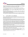
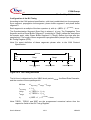
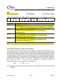
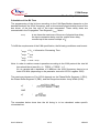
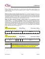
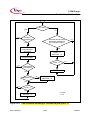
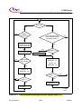
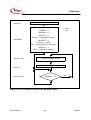
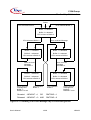
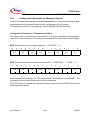
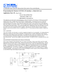
C164 Group
The On-Chip CAN Interface
19
The On-Chip CAN Interface
The Controller Area Network (CAN) bus with its associated protocol allows communication
between a number of stations which are connected to this bus with high efficiency.
Efficiency in this context means:
•
•
•
•
Transfer speed (Data rates of up to 1 Mbit/sec can be achieved)
Data integrity (The CAN protocol provides several means for error checking)
Host processor unloading (The controller here handles most of the tasks autonomously)
Flexible and powerful message passing (The extended CAN protocol is supported)
The integrated CAN module handles the completely autonomous transmission and
reception of CAN frames in accordance with the CAN specification V2.0 part B (active),
i.e. the on-chip CAN module can receive and transmit...
• Standard frames with 11-bit identifiers, as well as
• Extended frames with 29-bit identifiers.
Note: The CAN module is an XBUS peripheral and therefore requires bit XPEN in
register SYSCON to be set in order to be operable.
Core Registers
Control Registers
(within each module)
Object Registers
(within each module)
SYSCON
CSR
X
MCRn
X
SYSCON3E
PCIR
X
UARn
X
DP4
BTR
X
LARn
X
GMS
X
Data
X
ODP4
E
DP8
ODP8
Interrupt Control
XP0IC
E
U/LGML X
E
U/LMLM X
SYSCONSystem Configuration Register
SYSCON3Peripheral Management Control Register
DP4
Port 4 Direction Control Register
ODP4
Port 4 Open Drain Control Register
DP8
Port 8 Direction Control Register
ODP8
Port 8 Open Drain Control Register
XP0IC CAN1 Interrupt Control Register
CSR
PCIR
BTR
GMS
U/LGML
U/LMLM
MCRn
U/LARn
Control/Status Register
Port Control / Interrupt Register
Bit Timing Register
Global Mask Short
Global Mask Long
Last Message Mask
Configuration Register of Message n
Arbitration Register of Message n
Figure 19-1 Registers Associated with the CAN Module
User’s Manual
19-1
1999-09
C164 Group
The On-Chip CAN Interface
The bit timing is derived from the XCLK and is programmable up to a data rate of
1 MBaud. The minimum CPU clock frequency to achieve 1 MBaud is fCPU ≥ 8/16 MHz,
depending on the activation of the CAN module’s clock prescaler.
The CAN module uses two pins of Port 4 or Port 8 to interface to a bus transceiver.
It provides Full CAN functionality on up to 15 full sized message objects (8 data bytes
each). Message object 15 may be configured for Basic CAN functionality with a doublebuffered receive object.
Both modes provide separate masks for acceptance filtering which allows the
acceptance of a number of identifiers in Full CAN mode and also allows disregarding a
number of identifiers in Basic CAN mode.
All message objects can be updated independent from the other objects during operation
of the module and are equipped with buffers for the maximum message length of 8 bytes.
19.1
Functional Blocks of the CAN Module
The CAN module combines several functional blocks (see figure below) that work in
parallel and contribute to the controller’s performance. These units and the functions
they provide are described below.
Each of the message objects has a unique identifier and its own set of control and status
bits. Each object can be configured with its direction as either transmit or receive, except
the last message which is only a double receive buffer with a special mask register.
An object with its direction set as transmit can be configured to be automatically sent
whenever a remote frame with a matching identifier (taking into account the respective
global mask register) is received over the CAN bus. By requesting the transmission of a
message with the direction set as receive, a remote frame can be sent to request that
the appropriate object be sent by some other node. Each object has separate transmit
and receive interrupts and status bits, giving the CPU full flexibility in detecting when a
remote/data frame has been sent or received.
For general purpose two masks for acceptance filtering can be programmed, one for
identifiers of 11 bits and one for identifiers of 29 bits. However the CPU must configure
bit XTD (Normal or Extended Frame Identifier) for each valid message to determine
whether a standard or extended frame will be accepted.
The last message object has its own programmable mask for acceptance filtering,
allowing a large number of infrequent objects to be handled by the system.
The object layer architecture of the CAN controller is designed to be as regular and
orthogonal as possible. This makes it easy to use.
User’s Manual
19-2
1999-09
C164 Group
The On-Chip CAN Interface
Tx/Rx Shift Register
The Transmit / Receive Shift Register holds the destuffed bit stream from the bus line to
allow the parallel access to the whole data or remote frame for the acceptance match
test and the parallel transfer of the frame to and from the Intelligent Memory.
Bit Stream Processor
The Bit Stream Processor (BSP) is a sequencer controlling the sequential data stream
between the Tx/Rx Shift Register, the CRC Register, and the bus line. The BSP also
controls the EML and the parallel data stream between the Tx/Rx Shift Register and the
Intelligent Memory such that the processes of reception, arbitration, transmission, and
error signalling are performed according to the CAN protocol. Note that the automatic
retransmission of messages which have been corrupted by noise or other external error
conditions on the bus line is handled by the BSP.
Cyclic Redundancy Check Register
This register generates the Cyclic Redundancy Check (CRC) code to be transmitted
after the data bytes and checks the CRC code of incoming messages. This is done by
dividing the data stream by the code generator polynomial.
Error Management Logic
The Error Management Logic (EML) is responsible for the fault confinement of the CAN
device. Its counters, the Receive Error Counter and the Transmit Error Counter, are
incremented and decremented by commands from the Bit Stream Processor. According
to the values of the error counters, the CAN controller is set into the states error active,
error passive and busoff.
The CAN controller is error active, if both error counters are below the error passive limit of 128.
It is error passive, if at least one of the error counters equals or exceeds 128.
It goes busoff, if the Transmit Error Counter equals or exceeds the busoff limit of 256.
The device remains in this state, until the busoff recovery sequence is finished.
Additionally, there is the bit EWRN in the Status Register, which is set, if at least one of
the error counters equals or exceeds the error warning limit of 96. EWRN is reset, if both
error counters are less than the error warning limit.
User’s Manual
19-4
1999-09
C164 Group
The On-Chip CAN Interface
Bit Timing Logic
This block (BTL) monitors the busline input CAN_RXD and handles the busline related
bit timing according to the CAN protocol.
The BTL synchronizes on a recessive to dominant busline transition at Start of Frame
(hard synchronization) and on any further recessive to dominant busline transition, if the
CAN controller itself does not transmit a dominant bit (resynchronization).
The BTL also provides programmable time segments to compensate for the propagation
delay time and for phase shifts and to define the position of the Sample Point in the bit
time. The programming of the BTL depends on the baudrate and on external physical
delay times.
Intelligent Memory
The Intelligent Memory (CAM/RAM Array) provides storage for up to 15 message objects
of maximum 8 data bytes length. Each of these objects has a unique identifier and its
own set of control and status bits. After the initial configuration, the Intelligent Memory
can handle the reception and transmission of data without further CPU actions.
Organization of Registers and Message Objects
All registers and message objects of the CAN controller are located in the special CAN
address area of 256 bytes, which is mapped into segment 0 and uses
addresses00’EF00H through 00’EFFFH. All registers are organized as 16-bit registers,
located on word addresses. However, all registers may be accessed bytewise in order
to select special actions without effecting other mechanisms.
Register Naming reflects the specific name of a register as well as a general module
indicator. This results in unique register names.
Example: module indicator is C1 (CAN module 1), specific name is Control/Status
Register (CSR), unique register name is C1CSR.
Note: The address map shown below lists the registers which are part of the CAN
controller. There are also C164 specific registers that are associated with the CAN
module.
User’s Manual
19-5
1999-09
C164 Group
The On-Chip CAN Interface
EF00H
EF10H
EF20H
EF30H
EF40H
EF50H
EF60H
General Registers
Control/Status
Register CSR
Message Object 1
Message Object 2
Port Ctrl./Interrupt
Reg. PCIR
Message Object 3
Message Object 4
Message Object 5
Message Object 6
EF70H
Message Object 7
EF80H
Message Object 8
EF90H
Message Object 9
EFA0H
Message Object 10
EFB0H
Message Object 11
EFC0H
Message Object 12
EFD0H
Message Object 13
EFE0H
Message Object 14
EFF0H
Message Object 15
EF00H
EF02H
Bit Timing Register
BTR
EF04H
Global Mask Short
GMS
EF06H
EF08H
Global Mask Long
LGML
UGML
Mask of Last
Message
EF0CH
LMLM
UMLM
CAN Address Area
General Registers
Figure 19-3 CAN Module Address Map
User’s Manual
19-6
1999-09
C164 Group
The On-Chip CAN Interface
19.2
General Functional Description
The Control / Status Register (CSR) accepts general control settings for the module and
provides general status information.
CSR
Control / Status Register
15
14
12
11
-
RX
OK
TX
OK
LEC
TM CCE
0
r
rwh
rwh
rwh
rw
r
rh
10
9
8
7
Reset value: XX01H
13
B
E
OFF WRN
rh
XReg (EF00H)
6
rw
5
4
3
CPS EIE
rw
rw
2
1
0
SIE
IE
INIT
rw
rw
rwh
Bit
Function (Control Bits)
INIT
Initialization
Starts the initialization of the CAN controller, when set.
INIT is set -after a reset
-when entering the busoff state
-by the application software
IE
Interrupt Enable
Enables or disables interrupt generation from the CAN module via the
signal XINTR. Does not affect status updates.
SIE
Status Change Interrupt Enable
Enables or disables interrupt generation when a message transfer
(reception or transmission) is successfully completed or a CAN bus error
is detected (and registered in the status partition).
EIE
Error Interrupt Enable
Enables or disables interrupt generation on a change of bit BOFF or
EWARN in the status partition).
CPS
Clock Prescaler Control Bit
0:
Standard mode: the input clock is divided 2:1. The minimum
input frequency to achieve a baudrate of 1 MBaud is fCPU = 16 MHz.
1:
Fast mode: the input clock is used directly 1:1. The minimum
input frequency to achieve a baudrate of 1 MBaud is fCPU = 8 MHz.
CCE
Configuration Change Enable
Allows or inhibits CPU access to the Bit Timing Register.
TM
Test Mode (must be ’0’)
Make sure that this bit is always cleared when writing to the Control
Register, as this bit controls a special test mode, that is used for
production testing. During normal operation, however, this test mode
may lead to undesired behaviour of the device.
User’s Manual
19-7
1999-09
C164 Group
The On-Chip CAN Interface
Bit
Function (Status Bits)
LEC
Last Error Code
This field holds a code which indicates the type of the last error occurred
on the CAN bus. If a message has been transferred (reception or
transmission) without error, this field will be cleared.
0
No Error
1
Stuff Error: More than 5 equal bits in a sequence have occurred
in a part of a received message where this is not allowed.
2
Form Error: Wrong format in fixed format part of a received frame.
3
AckError: The message this CAN controller transmitted was not
acknowledged by another node.
4
Bit1Error: During the transmission of a message (with the
exception of the arbitration field), the device wanted to send a
recessive level (“1”), but the monitored bus value was dominant.
5
Bit0Error: During the transmission of a message (or acknowledge
bit, active error flag, or overload flag), the device wanted to send a
dominant level (“0”), but the monitored bus value was recessive.
During busoff recovery this status is set each time a sequence of
11 recessive bits has been monitored. This enables the CPU to
monitor the proceeding of the busoff recovery sequence (indicates
that the bus is not stuck at dominant or continously disturbed).
6
CRCError: The received CRC check sum was incorrect.
7
Unused code: may be written by the CPU to check for updates.
TXOK
Transmitted Message Successfully
Indicates that a message has been transmitted successfully (error free
and acknowledged by at least one other node), since this bit was last
reset by the CPU (the CAN controller does not reset this bit!).
RXOK
Received Message Successfully
This bit is set each time a message has been received successfully,
since this bit was last reset by the CPU (the CAN controller does not
reset this bit!).
RXOK is also set when a message is received that is not accepted (i.e. stored).
EWRN
Error Warning Status
Indicates that at least one of the error counters in the EML has reached
the error warning limit of 96.
BOFF
Busoff Status
Indicates when the CAN controller is in busoff state (see EML).
Note: Reading the upper half of the Control Register (status partition) will clear the
Status Change Interrupt value in the Interrupt Register, if it is pending.
Use byte accesses to the lower half to avoid this.
User’s Manual
19-8
1999-09
C164 Group
The On-Chip CAN Interface
CAN Interrupt Handling
The on-chip CAN module has one interrupt output, which is connected (through a
synchronization stage) to a standard interrupt node in the C164 in the same manner as
all other interrupts of the standard on-chip peripherals. With this configuration, the user
has all control options available for this interrupt, such as enabling/disabling, level and
group priority, and interrupt or PEC service (see note below). The on-chip CAN module
is connected to an XBUS interrupt control register.
As for all other interrupts, the node interrupt request flag is cleared automatically by
hardware when this interrupt is serviced (either by standard interrupt or PEC service).
Note: As a rule, CAN interrupt requests can be serviced by a PEC channel. However,
because PEC channels only can execute single predefined data transfers (there
are no conditional PEC transfers), PEC service can only be used, if the request is
known to be generated by one specific source, and that no other interrupt request
will be generated in between. In practice this seems to be a rare case.
Since an interrupt request of the CAN module can be generated due to different
conditions, the appropriate CAN interrupt status register must be read in the service
routine to determine the cause of the interrupt request. The interrupt identifier INTID (a
number) in the Port Control / Interrupt Register (PCIR) indicates the cause of an
interrupt. When no interrupt is pending, the identifier will have the value 00H.
If the value in INTID is not 00H, then there is an interrupt pending. If bit IE in the control/
status register is set also the interrupt signal to the CPU is activated. The interrupt signal
(to the interrupt node) remains active until INTID gets 00H (i.e. all interrupt requests have
been serviced) or until interrupt generation is disabled (CSR.IE = ’0’).
Note: The interrupt node is activated only upon a 0-->1 transition of the CAN interrupt
signal. The CAN interrupt service routine should only be left after INTID has been
verified to be 00H.
The interrupt with the lowest number has the highest priority. If a higher priority interrupt
(lower number) occurs before the current interrupt is processed, INTID is updated and
the new interrupt overrides the last one.
INTID is also updated when the respective source request has been processed. This is
indicated by clearing the INTPND flag in the respective object’s message control register
(MCRn) or by reading the status partition of register CSR (in case of a status change
interrupt). The updating of INTID is done by the CAN state machine and takes up to 6
CAN clock cycles (1 CAN clock cycle = 1 or 2 CPU clock cycles, determined by the
prescaler bit CPS), depending on current state of the state machine.
Note: A worst case condition can occur when BRP = 00H AND the CAN controller is storing
a just received message AND the CPU is executing consecutive accesses to the CAN
module. In this rare case the maximum delay may be 26 CAN clock cycles.
The impact of this delay can be minimized by clearing bit INTPND at an early stage
User’s Manual
19-9
1999-09
C164 Group
The On-Chip CAN Interface
of interrupt processing, and (if required) restricting CPU accesses to the CAN
module until the anticipated updating is complete.
PCIR
Port Control / Interrupt Register XReg (EF02H)
15
14
13
12
11
- reserved -
-
Bit
INTID
IPC
-
-
-
10
9
8
7
Reset value: XXXXH
6
5
4
3
IPC
INTID
rw
rh
2
1
0
Function
Interrupt Identifier
This number indicates the cause of the interrupt (if pending).
Interrupt Idle: There is no interrupt request pending.
00H
Status Change Interrupt: The CAN controller has updated (not
01H
necessarily changed) the status in the Control Register. This can
refer to a change of the error status of the CAN controller (EIE is
set and BOFF or EWRN change) or to a CAN transfer incident
(SIE must be set), like reception or transmission of a message
(RXOK or TXOK is set) or the occurrence of a CAN bus error
(LEC is updated). The CPU may clear RXOK, TXOK, and LEC,
however, writing to the status partition of the Control Register
can never generate or reset an interrupt. To update the INTID
value the status partition of the Control Register must be read.
Message 15 Interrupt: Bit INTPND in the Message Control
02H
Register of message object 15 (last message) has been set.
The last message object has the highest interrupt priority of all
message objects. 1)
(02+N) Message N Interrupt: Bit INTPND in the Message Control
Register of message object ‘N’ has been set (N = 1...14). Note
that a message interrupt code is only displayed, if there is no
other interrupt request with a higher priority. 1)
Example: message 1: INTID = 03H, message 14: INTID = 10H
Interface Port Control (reset value = 111B, i.e. no port connection)
The encoding of bitfield IPC is described in section “The CAN Application
Interface“.
Note: Bitfield IPC can be written only while bit CCE is set.
1) Bit INTPND of the corresponding message object has to be cleared to give messages with a lower priority the
possibility to update INTID or to reset INTID to “00H” (idle state).
User’s Manual
19-10
1999-09
C164 Group
The On-Chip CAN Interface
Configuration of the Bit Timing
According to the CAN protocol specification, a bit time is subdivided into four segments:
Sync segment, propagation time segment, phase buffer segment 1 and phase buffer
segment 2.
Each segment is a multiple of the time quantum tq, with tq = (BRP+1) * 2(1-CPS) * tXCLK.
The Synchronization Segment (Sync Seg) is always 1 tq long. The Propagation Time
Segment and the Phase Buffer Segment 1 (combined to TSeg1) define the time before
the sample point, while Phase Buffer Segment 2 (TSeg2) defines the time after the
sample point. The length of these segments is programmable (except Sync-Seg) via the
Bit Timing Register (BTR).
Note: For exact definition of these segments please refer to the CAN Protocol
Specification.
1 bit time
SyncSeg
TSeg1
TSeg2
1 time quantum
( tq )
sample point
SyncSeg
transmit point
Figure 19-4 Bit Timing Definition
, the Baud Rate Prescaler,
The bit time is determined by the XBUS clock period t
XCLK
and the number of time quanta per bit:
bit time
= tSync-Seg + tTSeg1 + tTSeg2
tSync-Seg
= 1 • tq
tTSeg1
= ( TSEG1 + 1 ) • tq
tTSeg2
= ( TSEG2 + 1 ) • tq
tq
= ( BRP + 1 ) • 2(1-CPS) • tXCLK
Note: TSEG1, TSEG2, and BRP are the programmed numerical values from the
respective fields of the Bit Timing Register.
User’s Manual
19-11
1999-09
C164 Group
The On-Chip CAN Interface
BTR
Bit Timing Register
15
14
13
12
XReg (EF04H)
11
10
9
8
7
Reset value: UUUUH
6
5
4
3
2
0
TSEG2
TSEG1
SJW
BRP
r
rw
rw
rw
rw
Bit
BRP
1
0
Function
Baud Rate Prescaler
For generating the bit time quanta the CPU frequency fCPU is divided by
2(1-CPS) * (BRP+1). See also the prescaler control bit CPS in register CSR.
(Re)Synchronization Jump Width
Adjust the bit time by maximum (SJW+1) time quanta for
resynchronization.
Time Segment before sample point
There are (TSEG1+1) time quanta before the sample point.
Valid values for TSEG1 are “2...15”.
Time Segment after sample point
There are (TSEG2+1) time quanta after the sample point.
Valid values for TSEG2 are “1...7”.
SJW
TSEG1
TSEG2
Note: This register can only be written, if the config. change enable bit (CCE) is set.
Hard Synchronization and Resynchronization
To compensate phase shifts between clock oscillators of different CAN controllers, any
CAN controller has to synchronize on any edge from recessive to dominant bus level if
the edge lies between a Sample Point and the next Synchronization Segment, and on
any other edge if it itself does not send a dominant level. If the Hard Synchronization is
enabled (at the Start of Frame), the bit time is restarted at the Synchronization Segment,
otherwise the Resynchronization Jump Width (SJW) defines the maximum number of
time quanta by which a bit time may be shortened or lengthened during one
Resynchronization. The current bit time is adjusted by
tSJW
= ( SJW + 1 ) • tq
Note: SJW is the programmed numerical value from the respective field of the Bit Timing
Register.
User’s Manual
19-12
1999-09
C164 Group
The On-Chip CAN Interface
Calculation of the Bit Time
The programming of the bit time according to the CAN Specification depends on the
desired baudrate, the XCLK frequency, and on the external physical delay times of the
bus driver, of the bus line and of the input comparator. These delay times are
summarized in the Propagation Time Segment tProp, where
tProp
is two times the maximum of the sum of physical bus delay,
the input comparator delay, and the output driver delay
rounded up to the nearest multiple of tq.
To fulfill the requirements of the CAN specification, the following conditions must be met:
tTSeg2 ≥ 2•tq = Information Processing Time
tTSeg2 ≥ tSJW
tTSeg1 ≥ 3•tq
tTSeg1 ≥ tSJW + tProp
Note: In order to achieve correct operation according to the CAN protocol the total bit
time should be at least 8 tq, i.e. TSEG1 + TSEG2 ≥ 5.
So, to operate with a baudrate of 1 MBit/sec, the XCLK frequency has to be at
least 8/16 MHz (depending on the prescaler control bit CPS in register CSR).
The maximum tolerance df for XCLK depends on the Phase Buffer Segment 1 (PB1),
the Phase Buffer Segment 2 (PB2), and the Resynchronization Jump Width (SJW):
df
≤
min ( PB1, PB2 )
--------------------------------------------------2 × ( 13 × bit time – PB2 )
AND
df
≤
t SJW
----------------------20 × bit time
The examples below show how the bit timing is to be calculated under specific
circumstances.
User’s Manual
19-13
1999-09
C164 Group
The On-Chip CAN Interface
Bit Timing Example for High Baudrate
This example makes the following assumptions:
• XCLK frequency = 20 MHz
• BRP = 00, CPS = 0
• Baudrate = 1 Mbit/sec
tq
bus driver delay
receiver circuit delay
bus line (40 m) delay
tProp
tSJW
tTSeg1
tTSeg2
tSync
tBit
tolerance for fXCLK
100 ns
50 ns
30 ns
220 ns
600 ns
100 ns
700 ns
200 ns
100 ns
= 2 • tXCLK
= 6 • tq
= 1 • tq
= tProp + tSJW
= Information Processing Time
= 1 • tq
1000 ns = tSync + tTSeg1 + tTSeg2
0.39%
min ( PB1, PB2 )
= -----------------------------------------------------------2 × ( 13 × bit time – PB2 )
=
0,1µs
------------------------------------------------------2 × ( 13 × 1µs – 0,2µs )
Bit Timing Example for Low Baudrate
This example makes the following assumptions:
• XCLK frequency = 4 MHz
• BRP = 01, CPS = 0
• Baudrate = 100 kbit/sec
tq
bus driver delay
receiver circuit delay
bus line (40 m) delay
tProp
tSJW
tTSeg1
tTSeg2
tSync
tBit
tolerance for fXCLK
1 µs
200 ns
80 ns
220 ns
1 µs
4 µs
5 µs
4 µs
1 µs
= 4 • tXCLK
10 µs
= tSync + tTSeg1 + tTSeg2
1.58%
min ( PB1, PB2 )
= -----------------------------------------------------------2 × ( 13 × bit time – PB2 )
= 1 • tq
= 4 • tq
= tProp + tSJW
= Information Processing Time + 2 • tq
= 1 • tq
4µs
= -----------------------------------------------------2 × ( 13 × 10µs – 4µs )
User’s Manual
19-14
1999-09
C164 Group
The On-Chip CAN Interface
Mask Registers
Messages can use standard or extended identifiers. Incoming frames are masked with
their appropriate global masks. Bit IDE of the incoming message determines, if the
standard 11-bit mask in Global Mask Short (GMS) is to be used, or the 29-bit extended
mask in Global Mask Long (UGML&LGML). Bits holding a “0” mean “don’t care”, i.e. do
not compare the message’s identifier in the respective bit position.
The last message object (15) has an additional individually programmable acceptance
mask (Mask of Last Message, UMLM&LMLM) for the complete arbitration field. This
allows classes of messages to be received in this object by masking some bits of the
identifier.
Note: The Mask of Last Message is ANDed with the Global Mask that corresponds to
the incoming message.
GMS
Global Mask Short
15
14
13
XReg (EF06H)
7
Reset value: UFUUH
12
11
10
9
8
6
5
4
3
ID20...18
1
1
1
1
1
ID28...21
rw
r
r
r
r
r
rw
Bit
Function
ID28...18
Identifier (11-bit)
Mask to filter incoming messages with standard identifier.
User’s Manual
19-15
2
1
0
1999-09
C164 Group
The On-Chip CAN Interface
UGML
Upper Global Mask Long
15
14
13
12
11
XReg (EF08H)
10
9
14
13
7
6
5
4
3
ID20...13
ID28...21
rw
rw
LGML
Lower Global Mask Long
15
8
Reset value: UUUUH
12
11
XReg (EF0AH)
7
9
8
6
5
4
3
ID4...0
0
0
0
ID12...5
rw
r
r
r
rw
Bit
Function
ID28...0
Identifier (29-bit)
Mask to filter incoming messages with extended identifier.
15
14
13
12
11
10
XReg (EF0CH)
9
7
6
5
4
3
ID17...13
ID28...21
rw
rw
rw
14
13
12
11
XReg (EF0EH)
7
0
2
1
0
Reset value: UUUUH
ID20...18
LMLM
Lower Mask of Last Message
15
8
1
Reset value: UUUUH
10
UMLM
Upper Mask of Last Message
2
2
1
0
Reset value: UUUUH
10
9
8
6
5
4
3
ID4...0
0
0
0
ID12...5
rw
r
r
r
rw
2
1
0
Bit
Function
ID28...0
Identifier (29-bit)
Mask to filter the last incoming message (Nr. 15) with standard or
extended identifier (as configured).
User’s Manual
19-16
1999-09
C164 Group
The On-Chip CAN Interface
19.3
The Message Object
The message object is the primary means of communication between CPU and CAN
controller. Each of the 15 message objects uses 15 consecutive bytes (see map below)
and starts at an address that is a multiple of 16.
Note: All message objects must be initialized by the CPU, even those which are not
going to be used, before clearing the INIT bit.
Offset
+0
Message Control (MCR)
+2
Arbitration (UAR&LAR)
Data0
Object Start Address (EFn0H)
Msg. Config. (MCFG)
+4
Message object 1: EF10H
+6
Message object 2: EF20H
...
Data2
Data1
+8
Data4
Data3
+10
Message object 14: EFE0H
Data6
Data5
+12
Message object 15: EFF0H
Reserved
Data7
+14
Figure 19-5 Message Object Address Map
The general properties of a message object are defined via the Message Control
Register (MCR). There is a dedicated register MCRn for each message object n.
Each element of the Message Control Register is made of two complementary bits.This
special mechanism allows the selective setting or resetting of specific elements (leaving
others unchanged) without requiring read-modify-write cycles. None of these elements
will be affected by reset.
The table below shows how to use and interpret these 2-bit fields.
Table 19-1
MCR Bitfield Encoding
Value Function on Write
Meaning on Read
00
-reserved-
-reserved-
01
Reset element
Element is reset
10
Set element
Element is set
11
Leave element unchanged
-reserved-
User’s Manual
19-17
1999-09
C164 Group
The On-Chip CAN Interface
MCRn
Message Control Register
15
14
13
12
11
XReg (EFn0H)
10
9
8
7
Reset value: UUUUH
6
5
4
3
2
1
0
RMTPND
TXRQ
MSGLST
CPUUPD
NEWDAT
MSGVAL
TXIE
RXIE
INTPND
rw
rw
rw
rw
rw
rw
rw
rw
Bit
Function
INTPND
Interrupt Pending
Indicates, if this message object has generated an interrupt request (see
TXIE and RXIE), since this bit was last reset by the CPU, or not.
RXIE
Receive Interrupt Enable
Defines, if bit INTPND is set after successful reception of a frame.
TXIE
Transmit Interrupt Enable
Defines, if bit INTPND is set after successful transmission of a frame. 1)
MSGVAL
Message Valid
Indicates, if the corresponding message object is valid or not. The CAN
controller only operates on valid objects. Message objects can be tagged
invalid, while they are changed, or if they are not used at all.
NEWDAT
New Data
Indicates, if new data has been written into the data portion of this
message object by CPU (transmit-objects) or CAN controller (receiveobjects) since this bit was last reset, or not. 2)
MSGLST
Message Lost (This bit applies to receive-objects only!)
Indicates that the CAN controller has stored a new message into this
object, while NEWDAT was still set, i.e. the previously stored message
is lost.
CPUUPD
CPU Update (This bit applies to transmit-objects only!)
Indicates that the corresponding message object may not be transmitted
now. The CPU sets this bit in order to inhibit the transmission of a
message that is currently updated, or to control the automatic response
to remote requests.
TXRQ
Transmit Request
Indicates that the transmission of this message object is requested by
the CPU or via a remote frame and is not yet done. TXRQ can be
disabled by CPUUPD. 1) 3)
User’s Manual
19-18
1999-09
C164 Group
The On-Chip CAN Interface
Bit
Function
RMTPND
Remote Pending (Used for transmit-objects)
Indicates that the transmission of this message object has been
requested by a remote node, but the data has not yet been transmitted.
When RMTPND is set, the CAN controller also sets TXRQ. RMTPND
and TXRQ are cleared, when the message object has been successfully
transmitted.
1)
In message object 15 (last message) these bits are hardwired to “0” (inactive) in order to prevent transmission
of message 15.
2)
When the CAN controller writes new data into the message object, unused message bytes will be overwritten
by non specified values. Usually the CPU will clear this bit before working on the data, and verify that the bit is
still cleared once it has finished working to ensure that it has worked on a consistent set of data and not part
of an old message and part of the new message.
For transmit-objects the CPU will set this bit along with clearing bit CPUUPD. This will ensure that, if the
message is actually being transmitted during the time the message was being updated by the CPU, the CAN
controller will not reset bit TXRQ. In this way bit TXRQ is only reset once the actual data has been transferred.
3) When the CPU requests the transmission of a receive-object, a remote frame will be sent instead of a data frame
to request a remote node to send the corresponding data frame. This bit will be cleared by the CAN controller
along with bit RMTPND when the message has been successfully transmitted, if bit NEWDAT has not been
set.
If there are several valid message objects with pending transmission request, the message with the lowest
message number is transmitted first. This arbitration is done when several objects are requested for
transmission by the CPU, or when operation is resumed after an error frame or after arbitration has been lost.
Arbitration Registers
The Arbitration Registers (UARn&LARn) are used for acceptance filtering of incoming
messages and to define the identifier of outgoing messages. A received message with
a matching identifier is accepted as a data frame (matching object has DIR=’0’) or as a
remote frame (matching object has DIR=’1’). For matching, the corresponding Global
Mask has to be considered (in case of message object 15 also the Mask of Last
Message). Extended frames (using Global Mask Long) can be stored only in message
objects with XTD=’1’, standard frames (using Global Mask Short) only in message
objects with XTD=’0’.
Message objects should have unique identifiers, i.e. if some bits are masked out by the
Global Mask Registers (i.e. “don’t care”), then the identifiers of the valid message objects
should differ in the remaining bits which are used for acceptance filtering.
If a received message (data frame or remote frame) matches with more than one valid
message object, it is associated with the object with the lowest message number. I.e. a
received data frame is stored in the “lowest” object, or the “lowest” object is sent in
response to a remote frame. The Global Mask is used for matching here.
User’s Manual
19-19
1999-09
C164 Group
The On-Chip CAN Interface
After a transmission (data frame or remote frame) the transmit request flag of the
matching object with the lowest message number is cleared. The Global Mask is not
used in this case.
When the CAN controller accepts a data frame, the complete message is stored into
the corresponding message object, including the identifier (also masked bits, standard
identifiers have bits ID17-0 filled with ’0’), the data length code (DLC), and the data bytes
(valid bytes indicated by DLC). This is implemented to keep the data bytes connected
with the identifier, even if arbitration mask registers are used.
When the CAN controller accepts a remote frame, the corresponding transmit
message object (1...14) remains unchanged, except for bits TXRQ and RMTPND, which
are set, of course. In the last message object 15 (which cannot start a transmission) the
identifier bits corresponding to the “don’t care” bits of the Last Message Mask are copied
from the received frame. Bits corresponding to the “don’t care” bits of the corresponding
global mask are not copied (i.e. bits masked out by the global and the last message
mask cannot be retrieved from object 15).
UARn
Upper Arbitration Register
15
14
13
12
11
ID20...18
XReg (EFn2H)
10
9
8
7
Reset value: UUUUH
6
5
ID17...13
4
13
12
1
0
rw
LARn
Lower Arbitration Register
14
2
ID28...21
rw
15
3
11
XReg (EFn4H)
7
Reset value: UUUUH
10
9
8
6
5
4
3
ID4...0
0
0
0
ID12...5
rw
r
r
r
rw
2
1
0
Bit
Function
ID28...0
Identifier (29-bit)
Identifier of a standard message (ID28...18) or an extended message
(ID28...0). For standard identifiers bits ID17...0 are “don’t care”.
User’s Manual
19-20
1999-09
C164 Group
The On-Chip CAN Interface
Message Configuration
The Message Configuration Register (low byte of MCFGn) holds a description of the
message within this object.
Note: There is no “don’t care” option for bits XTD and DIR. So incoming frames can only
match with corresponding message objects, either standard (XTD=0) or extended
(XTD=1). Data frames only match with receive-objects, remote frames only match
with transmit-objects.
When the CAN controller stores a data frame, it will write all the eight data bytes
into a message object. If the data length code was less than 8, the remaining bytes
of the message object will be overwritten by non specified values.
MCFGn
Message Configuration Reg.
15
14
13
12
11
10
XReg (EFn6H)
9
8
7
Reset value: - - UUH
6
5
Data Byte 0
DLC
rw
rw
4
3
2
DIR XTD
rw
rw
1
0
0
0
r
r
Bit
Function
XTD
Extended Identifier
0:
Standard
This message object uses a standard 11-bit identifier.
1:
Extended
This message object uses an extended 29-bit identifier.
DIR
Message Direction
0:
Receive object.
On TXRQ, a remote frame with the identifier of this message
object is transmitted.
On reception of a data frame with matching identifier, that
message is stored in this message object.
1:
Transmit object.
On TXRQ, the respective message object is transmitted.
On reception of a remote frame with matching identifier, the TXRQ
and RMTPND bits of this message object are set.
DLC
Data Length Code
Defines the number of valid data bytes within the data area.
Valid values for the data length are 0...8.
Note: The first data byte occupies the upper half of the message configuration register.
User’s Manual
19-21
1999-09
C164 Group
The On-Chip CAN Interface
Data Area
The data area occupies 8 successive byte positions after the Message Configuration
Register, i.e. the data area of message object n covers locations 00’EFn7H through
00’EFnEH.
Location 00’EFnFH is reserved.
Message data for message object 15 (last message) will be written into a two-messagealternating buffer to avoid the loss of a message, if a second message has been
received, before the CPU has read the first one.
Handling of Message Objects
The following diagrams summarize the actions that have to be taken in order to transmit
and receive messages over the CAN bus. The actions taken by the CAN controller are
described as well as the actions that have to be taken by the CPU (i.e. the servicing
program).
The diagrams show...
•
•
•
•
•
•
CAN controller handling of transmit objects
CAN controller handling of receive objects
CPU handling of transmit objects
CPU handling of receive objects
CPU handling of last message object
Handling of the last message’s alternating buffer
User’s Manual
19-22
1999-09
C164 Group
The On-Chip CAN Interface
bus free ?
yes
no
no
TXRQ=1
CPUUPD=0
received remote frame
with same identifier as
this message object ?
yes
NEWDAT := 0
load message
into buffer
no
yes
TXRQ := 1
RMTPND := 1
send message
RXIE = 1
no
yes
transmission
successful?
INTPND := 1
yes
NEWDAT=1
no
no
TXRQ := 0
RMTPND := 0
yes
no
TXIE = 1
yes
0: reset
1: set
INTPND := 1
Figure 19-6 CAN Controller Handling of Transmit Objects (DIR = ’1’)
User’s Manual
19-23
1999-09
C164 Group
The On-Chip CAN Interface
bus idle ?
yes
no
TXRQ=1
CPUUPD=0
no
received frame with
same identifier as this
message object ?
yes
NEWDAT := 0
load identifier and
control into buffer
no
yes
yes
NEWDAT = 1
send remote frame
MSGLST := 1
no
no
store message
NEWDAT := 1
TXRQ := 0
RMTPND := 0
transmission
successful?
yes
TXRQ := 0
RMTPND := 0
RXIE = 1
no
no
yes
TXIE = 1
yes
INTPND := 1
INTPND := 1
0: reset
1: set
Figure 19-7 CAN Controller Handling of Receive Objects (DIR = ’0’)
User’s Manual
19-24
1999-09
C164 Group
The On-Chip CAN Interface
( all bits undefined )
Power Up
TXIE := ( application specific )
RXIE := ( application specific )
INTPND := 0
RMTPND := 0
TXRQ := 0
CPUUPD := 1
Identifier := ( application specific )
NEWDAT := 0
Direction := transmit
DLC := ( application specific )
MSGVAL := 1
XTD := ( application specific )
Initialization
0: reset
1: set
CPUUPD := 1
Update : Start
NEWDAT := 1
Update
write / calculate message contents
CPUUPD := 0
Update : End
yes
want to send ?
TXRQ := 1
no
yes
no
update message ?
Figure 19-8 CPU Handling of Transmit Objects (DIR = ’1’)
User’s Manual
19-25
1999-09
C164 Group
The On-Chip CAN Interface
Power Up
Initialization
( all bits undefined )
TXIE := ( application specific )
RXIE := ( application specific )
INTPNDd := 0
RMTPND := 0
TXRQ := 0
MSGLST := 0
Identifier := ( application specific )
NEWDAT := 0
Direction := receive
DLC := ( value of DLC in transmitter )
MSGVAL := 1
XTD := ( application specific )
0: reset
1: set
NEWDAT := 0
Process : Start
process message contents
Process
NEWDAT = 1 ?
Process : End
yes
Restart Process
no
no
request update ?
yes
TXRQ := 1
Figure 19-9 CPU Handling of Receive Objects (DIR = ’0’)
User’s Manual
19-26
1999-09
C164 Group
The On-Chip CAN Interface
Power Up
( all bits undefined )
RXIE := ( application specific )
INTPND := 0
0: reset
1: set
RMTPND := 0
MSGLST := 0
Identifier := ( application specific )
Initialization
NEWDAT := 0
Direction := receive
DLC := ( value of DLC in transmitter )
MSGVAL := 1
XTD := ( application specific )
Process : Start
process message contents
NEWDAT := 0
Process
Process : End
NEWDAT = 1 ?
yes
Restart Process
no
Figure 19-10 CPU Handling of the Last Message Object
User’s Manual
19-27
1999-09
C164 Group
The On-Chip CAN Interface
Reset
CPU releases Buffer 2
CPU releases Buffer 1
Buffer 1 = released
Buffer 2 = released
CPU access to Buffer 2
CPU allocates Buffer 2
Store received Message
into Buffer 1
Buffer 1 = released
Buffer 1 = allocated
Buffer 2 = allocated
Buffer 2 = released
CPU access to Buffer 2
CPU access to Buffer 1
Store received
Message
into Buffer 1
Store received
Message
into Buffer 2
Buffer 1 = allocated
Buffer 1 = allocated
Buffer 2 = allocated
Buffer 2 = allocated
CPU access to Buffer 2
CPU access to Buffer 1
CPU releases
Buffer 2
CPU releases
Buffer 1
Allocated : NEWDAT = 1 OR
RMTPND = 1
Released : NEWDAT = 0 AND
RMTPND = 0
Store received
message into
Buffer 1
MSGLST is set
Store received
message into
Buffer 2
MSGLST is set
Figure 19-11 Handling of the Last Message Object’s Alternating Buffer
User’s Manual
19-28
1999-09
C164 Group
The On-Chip CAN Interface
19.4
Controlling the CAN Module
The CAN module is controlled by the C164 via hardware signals (e.g. reset) and via
register accesses executed by software.
Accessing the On-chip CAN Module
The CAN module is implemented as an X-Peripheral and is therefore accessed like an
external memory or peripheral. That means that the registers of the CAN module can be
read and written using 16-bit or 8-bit direct or indirect MEM addressing modes. Also bit
handling is not supported via the XBUS. Since the XBUS, to which the CAN module is
connected, also represents the external bus, CAN accesses follow the same rules and
procedures as accesses to the external bus. CAN accesses cannot be executed in
parallel to external instruction fetches or data read/writes, but are arbitrated and inserted
into the external bus access stream.
Accesses to the CAN module use demultiplexed addresses, a 16-bit data bus (byte
accesses possible), two waitstates and no tristate waitstate.
The CAN address area starts at 00’EF00H and covers 256 Bytes. This area is decoded
internally, so none of the programmable address windows must be sacrificed in order to
access the on-chip CAN module.
The advantage of locating the CAN address area in segment 0 is that the CAN module
is accessible via data page 3, which is the 'system' data page, accessed usually through
the 'system' data page pointer DPP3. In this way, the internal addresses, such like SFRs,
internal RAM, and the CAN registers, are all located within the same data page and form
a contiguous address space.
Power Down Mode
If the C164 enters Power Down mode, the XCLK signal will be turned off which will stop
the operation of the CAN module. Any message transfer is interrupted. In order to ensure
that the CAN controller is not stopped while sending a dominant level (’0’) on the CAN
bus, the CPU should set bit INIT in the Control Register prior to entering Power Down
mode. The CPU can check if a transmission is in progress by reading bits TXRQ and
NEWDAT in the message objects and bit TXOK in the Control Register. After returning
from Power Down mode via hardware reset, the CAN module has to be reconfigured.
User’s Manual
19-29
1999-09
C164 Group
The On-Chip CAN Interface
Disabling the CAN Module
When the CAN module is disabled by setting bit CANDIS in register SYSCON3
(peripheral management) no register accesses are possible. Also the module’s logic
blocks are stopped and no CAN bus transfers are possible. After re-enabling the CAN
module (CANDIS=’0’) it must be reconfigured (as after returning from Power Down
mode).
Note: Incoming message frames can still be recognized (not received) in this case by
monitoring the receive line CAN_RXD. For this purpose the receive line
CAN_RXD can be connected to a fast external interrupt via register EXISEL.
CAN Module Reset
The on-chip CAN module is connected to the XBUS Reset signal. This signal is
activated, when the C164’s reset input is activated, when a software reset is executed,
and in case of a watchdog reset. Activating the CAN module’s reset line triggers a
hardware reset.
This hardware reset...
•
•
•
•
•
•
disconnects the CAN_TXD output from the port logic
clears the error counters
resets the busoff state
switches the Control Register’s low byte to 01H
leaves the Control Register’s high byte and the Interrupt Register undefined
does not change the other registers including the message objects (notified as UUUU)
Note: The first hardware reset after power-on leaves the unchanged registers in an
undefined state, of course.
The value 01H in the Control Register’s low byte prepares for the module
initialization.
CAN Module Activation
After a reset the CAN module is disabled. Before it can be used to receive or transmit
messages the application software must activate the CAN module.
Three actions are required for this purpose:
• General Module Enable globally activates the CAN module. This is done by setting
bit XPEN in register SYSCON.
• Pin Assignment selects a pair of port pins that connect the CAN module to the
external transceiver. This is done via bitfield IPC in register PCIR.
• Module Initialization determines the functionality of the CAN module (baudrate,
active objects, etc.). This is the major part of the activation and is described in the
following.
User’s Manual
19-30
1999-09
C164 Group
The On-Chip CAN Interface
Module Initialization
The module initialization is enabled by setting bit INIT in the control register CSR. This
can be done by the CPU via software, or automatically by the CAN controller on a
hardware reset, or if the EML switches to busoff state.
While INIT is set...
•
•
•
•
all message transfer from and to the CAN bus is stopped
the CAN transmit line CAN_TXD is “1” (recessive)
the control bits NEWDAT and RMTPND of the last message object are reset
the counters of the EML are left unchanged.
Setting bit CCE in addition, permits changing the configuration in the Bit Timing Register.
To initialize the CAN Controller, the following actions are required:
• configure the Bit Timing Register (CCE required)
• set the Global Mask Registers
• initialize each message object.
If a message object is not needed, it is sufficient to clear its message valid bit (MSGVAL),
i.e. to define it as not valid. Otherwise, the whole message object has to be initialized.
After the initialization sequence has been completed, the CPU clears bit INIT.
Now the BSP synchronizes itself to the data transfer on the CAN bus by waiting for the
occurrence of a sequence of 11 consecutive recessive bits (i.e. Bus Idle) before it can
take part in bus activities and start message transfers.
The initialization of the message objects is independent of the state of bit INIT and can
be done on the fly. The message objects should all be configured to particular identifiers
or set to “not valid” before the BSP starts the message transfer, however.
To change the configuration of a message object during normal operation, the CPU first
clears bit MSGVAL, which defines it as not valid. When the configuration is completed,
MSGVAL is set again.
User’s Manual
19-31
1999-09
C164 Group
The On-Chip CAN Interface
Busoff Recovery Sequence
If the device goes busoff, it will set bit BOFF and also set bit INIT of its own accord,
stopping all bus activities. To have the CAN module take part in the CAN bus activities
again, the bus-off recovery sequence must be started by clearing the bit INIT (via
software). Once INIT has been cleared, the module will then wait for 129 occurrences of
Bus Idle before resuming normal operation.
At the end of the busoff recovery sequence the Error Management Counters will be
reset. This will automatically clear bits BOFF and EWRN.
During the waiting time after the resetting of INIT each time a sequence of 11 recessive
bits has been monitored, a Bit0Error code is written to the Control Register, enabling
the CPU to check up whether the CAN bus is stuck at dominant or continously disturbed
and to monitor the proceeding of the busoff recovery sequence.
Note: An interrupt can be generated when entering the busoff state if bits IE and EIE are
set. The corresponding interrupt code in bitfield INTID is 01H.
The busoff recovery sequence cannot be shortened by setting or resetting INIT.
User’s Manual
19-32
1999-09
C164 Group
The On-Chip CAN Interface
19.5
Configuration Examples for Message Objects
The two examples below represent standard applications for using CAN messages. Both
examples assume that identifier and direction are already set up correctly.
The respective contents of the Message Control Register (MCR) are shown.
Configuration Example of a Transmission Object
This object shall be configured for transmission. It shall be transmitted automatically in
response to remote frames, but no receive interrupts shall be generated for this object.
MCR (Data bytes are not written completely --> CPUUPD = ’1’)
15
14
13
12
11
10
9
8
7
6
5
4
3
2
1
0
01
01
10
01
10
01
01
01
RMTPND
TXRQ
CPUUPD
NEWDAT
MSGVAL
TXIE
RXIE
INTPND
MCR (Remote frame was received in the meantime --> RMTPND = ’1’, TXRQ = ’1’)
15
14
13
12
11
10
9
8
7
6
5
4
3
2
1
0
10
10
10
01
10
01
01
01
RMTPND
TXRQ
CPUUPD
NEWDAT
MSGVAL
TXIE
RXIE
INTPND
After updating the message the CPU should clear CPUUPD and set NEWDAT. The
previously received remote request will then be answered.
If the CPU wants to transmit the message actively it should also set TXRQ (which should
otherwise be left alone).
User’s Manual
19-33
1999-09
C164 Group
The On-Chip CAN Interface
Configuration Example of a Reception Object
This object shall be configured for reception. A receive interrupt shall be generated each
time new data comes in. From time to time the CPU sends a remote request to trigger
the sending of this data from a remote node.
MCR (Message object is idle, i.e. waiting for a frame to be received)
15
14
13
12
11
10
9
8
7
6
5
4
3
2
1
0
01
01
01
01
10
01
10
01
RMTPND
TXRQ
MSGLST
NEWDAT
MSGVAL
TXIE
RXIE
INTPND
.
MCR (A data frame was received --> NEWDAT = ’1’, INTPND = ’1’)
15
14
13
12
11
10
9
8
7
6
5
4
3
2
1
0
01
01
01
10
10
01
10
10
RMTPND
TXRQ
MSGLST
NEWDAT
MSGVAL
TXIE
RXIE
INTPND
To process the message the CPU should clear INTPND and NEWDAT, process the
data, and check that NEWDAT is still clear after that. If not, the processing should be
repeated.
To send a remote frame to request the data, simply bit TXRQ needs to be set. This bit
will be cleared by the CAN controller, once the remote frame has been sent or if the data
is received before the CAN controller could transmit the remote frame.
User’s Manual
19-34
1999-09
C164 Group
The On-Chip CAN Interface
19.6
The CAN Application Interface
The on-chip CAN module of the C164 is connected to the (external) physical layer (i.e.
the CAN bus) via two signals:
Table 19-2
CAN Interface Signals
CAN Signal
Port Pin
CAN_RXD
Controlled via Receive data from the physical layer of the CAN bus.
C1PCIR.IPC Transmit data to the physical layer of the CAN bus.
CAN_TXD
Function
A logic low level (’0’) is interpreted as the dominant CAN bus level, a logic high level (’1’)
is interpreted as the recessive CAN bus level.
Connection to an External Transceiver
The CAN module of the C164 can be connected to an external CAN bus via a CAN
transceiver.
CAN1
CAN_RXD
CAN
Transceiver
CAN_TXD
Physical
Layer
CAN Bus
Note: Basically it is also possible to connect several CAN modules directly (on-board)
without using CAN transceivers.
C164
Figure 19-12 Connection to a Single CAN Bus
User’s Manual
19-35
1999-09
C164 Group
The On-Chip CAN Interface
Port Control
The receive data line and the transmit data line of the CAN module are alternate port
functions. Make sure that the respective port pin for the receive line is switched to input
in order to enable proper reception. The respective port driver for the transmit will
automatically be switched ON.
This provides a standard pin configuration without additional software control and also
works in emulation mode where the port direction registers cannot be controlled.
The receive and transmit line of the CAN module may be assigned to several port pins
of the C164 under software control. This assignment is selected via bitfield IPC (Interface
Port Connection) in register PCIR.
Table 19-3
Assignment of CAN Interface Lines to Port Pins
IPC
CAN_RXD
CAN_TXD
Notes
000
P4.5
P4.6
001
---
---
010
P8.0
P8.1
Port 4 available for segment address lines
A21...A16 (4 MByte external address space).
011
P8.2
P8.3
Port 4 available for segment address lines
A21...A16 (4 MByte external address space).
100
---
---
Reserved. Do not use this combination.
101
---
---
Reserved. Do not use this combination.
110
---
---
Reserved. Do not use this combination.
111
Idle
(recessive)
Compatible assignments (CAN1). 1)
Reserved. Do not use this combination.
Disconnected No port assigned. Default after Reset.
1) This assignment is compatible with previous derivatives where the assignment of CAN interface lines was
fixed.
User’s Manual
19-36
1999-09
C164 Group
The On-Chip CAN Interface
The location of the CAN interface lines can now be selected via software according to
the requirements of an application:
Compatible Assignment (IPC=000B) makes the C164 suitable for applications with a
given hardware (board layout). The CAN interface lines are connected to the port pins to
which they are hardwired in previous derivatives.
Full Address Assignment (IPC=010B or 011B) removes the CAN interface lines
completely from Port 4. The maximum external address space of 4 MByte is available in
this case.
The CAN interface lines are mapped to Port 8. Two pairs of Port 8 pins can be selected.
No Assignment (IPC=111B) disconnects the CAN interface lines from the port logic.
This avoids undesired currents through the interface pin drivers while the C164 is in a
power saving state.
After reset the CAN interface lines are disconnected.
Note: Assigning CAN interface signals to a port pin overrides the other alternate function
of the respective pin (segment address on Port 4, CAPCOM lines on Port 8).
User’s Manual
19-37
1999-09