1
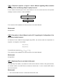
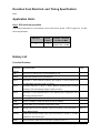
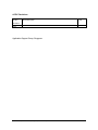
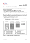
Microcontrollers
Errata Sheet
30 August 2001 / Release 1.4
Device:
C515C-L,
C515C-8R
Stepping Code / Marking:
Package:
AA
P-MQFP-80
This Errata Sheet describes the deviations from the current user documentation. The
classification and numbering system is module oriented in a continual ascending sequence
over several derivatives, as well already solved deviations are included. So gaps inside this
enumeration could occur.
The current documentation is: C515C User's Manual 11.97
C515C Data Sheet 07.99
Instruction Set Manual 05.98
Note: Devices marked with EES- or ES are engineering samples which may not be
completely tested in all functional and electrical characteristics, therefore they should
be used for evaluation only.
The specific test conditions for EES and ES are documented in a separate Status Sheet.
Change summary to last Errata Sheet Rel. 1.3:
•
Added new item numbered ROM.1.
Errata Sheet, C515C-L / -8R, Step AA, Release 1.4, HR
- 1 of 8 –
Functional Problems:
PIN.1: Pins 32 VCCE1 and 35 VSSE1 are not available for use
For the ROM / ROMless version, the pins 32 and 35 are NC (Not Connected) pins instead of VCCE1
and VSSE1. On the target board, whether these pins are connected or not to supply will not affect chip
performance and behavior.
Workaround:
None.
CAN.2: Unexpected Remote Frame Transmission
The on-chip CAN module may send an unexpected remote frame with the identifier=0, when a
pending transmit request of a message object is disabled by software.
There are three possibilities to disable a pending transmit request of a message object (n=1..14):
•
Set CPUUPDn element
•
Reset TXRQn element
•
Reset MSGVALn element
Either of these actions will prevent further transmissions of message object n.
The symptom described above occurs when the CPU accesses CPUUPD, TXRQ or MSGVAL, while
the pending transmit request of the corresponding message object is transferred to the CAN state
machine (just before start of frame transmission). At this particular time the transmit request is
transferred to the CAN state machine before the CPU prevents transmission. In this case the transmit
request is still accepted from the CAN state machine. However the transfer of the identifier, the data
length code and the data of the corresponding message object is prevented. Then the pre-charge
values of the internal “hidden buffer” are transmitted instead, this causes to a remote frame
transmission with identifier=0 (11 bit) and data length code=0.
This behavior occurs only when the transmit request of message object n is pending and the transmit
requests of other message objects are not active (single transmit request).
If this remote frame loses arbitration (to a data frame with identifier=0) or if it is disturbed by an error
frame, it is not retransmitted.
Errata Sheet, C515C-L / -8R, Step AA, Release 1.4, HR
- 2 of 8 –
Effects to other CAN nodes in the network
The effect leads to delays of other pending messages in the CAN network due to the high priority of
the Remote Frame. Furthermore the unexpected remote frame can trigger other data frames
depending on the CAN node’s configuration.
Workaround:
1.
The behavior can be avoided if a message object is not updated by software when a transmission
of the corresponding message object is pending (TXRQ element is set) and the CAN module is
active (INIT = 0). If a re-transmission of a message (e.g. after lost arbitration or after the
occurrence of an error frame) needs to be cancelled, the TXRQ element should be cleared by
software as soon as NEWDAT is reset from the CAN module.
2.
The nodes in the CAN system ignore the remote frame with the identifier=0 and no data frame is
triggered by this remote frame.
CAN.3: Description in User's Manual regarding the reception of remote frames and the
data length code (DLC) field is incorrect
It is inaccurately described in the User's Manual on page 6-94 under 'Arbitration Registers' that 'When
the CAN controller stores a remote frame, only the data length code is stored into the corresponding
message object'.
The correct should be that the DLC field remains unchanged in the receiving
message object, and that the CPU has the responsibility to define the DLC of the answering data
frame.
This correction will be updated to the future versions of the User's Manuals.
Workaround:
Not applicable.
Errata Sheet, C515C-L / -8R, Step AA, Release 1.4, HR
- 3 of 8 –
CAN.4: Flowchart sequence in figure in User's Manual regarding Micro-controller
handling of the Last Message Object is partly incorrect
For the software flowchart figure 6-48 in User's Manual 11.97, the correct would be to first 'process
message contents' and then to 'clear bit NEWDAT'.
process message contents
NEWDAT: = 0
This correction will be updated to the future versions of the User's Manuals.
Workaround:
Not applicable.
CAN.5: Description in User's Manual section 6.5.5 regarding the Configuration of the
Bit Timing is partly incorrect
As described for the CAN Bit Timing Register High BTR1, the minimum total time requirement for
segment 1 and segment 2 is as follows:
tTSeg1 ≥ 3 x tq,
tTSeg2 ≥ 2 x tq.
The total bit time remains at (t TSeg1 + t TSeg2 ≥ 7 x tq).
This correction will be updated to the future versions of the User's Manuals.
Workaround:
Not applicable.
WDT.1: Watchdog Timer is not halted in idle mode
The Watchdog Timer (WDT) is not halted in the idle mode as defined. However, during the idle mode,
an overflow condition of the WDT does not initiate an internal reset. In such a case the WDT starts a
new count sequence.
Workaround:
1.
Do not use the WDT function in combination with the idle mode.
Errata Sheet, C515C-L / -8R, Step AA, Release 1.4, HR
- 4 of 8 –
2.
In case of WDT is running before entry into idle mode, to avoid a WDT initiated reset upon exit of
the idle mode, the following methods can be used.
(A) The WDT is refreshed immediately upon exit from idle mode.
(B) A timed interrupt can be used to exit the idle mode before the WDT reaches the counter state
7FFCh.
This can be achieved by using Timer 0, 1 or 2.
This timer can be programmed to
generate an interrupt at a WDT counter state prior to overflow, for e.g., at 7F00h. Prior to entering
idle mode, the WDT can be refreshed and the timer 0, 1or 2 can be started immediately to
synchronize the WDT. In the interrupt service routine of the Timer 0, 1 or 2, the WDT must be
refreshed. If required, idle mode could be entered again.
OWD.1: The bit 7 (OWDS) of SFR IP0 cannot be set by software.
The bit 7 (OWDS) of SFR IP0 cannot be set by software. It is inaccurately stated in the manual that
this bit can be set by software.
Workaround:
None.
SWPD.1: Corrupt wake-up from software power down mode
The problem occurs under following conditions :
-
Wake-up from software power down mode through P3.2/INT0# pin is used
-
C515C-8R is clocked by the on-chip oscillator (with crystal or ceramic resonator)
During the start-up phase of the on-chip oscillator of a wake-up from software power down mode
procedure, which follows the latch phase of the P3.2/INT0# low signal, the oscillator watchdog unit
enables the clock signal to the CPU although the correct frequency of the clock oscillator has not been
reached. As a result, the CPU is fed with a clock signal which has irregular fast oscillations or wrong
clock pulses. This wrong internal clock signal causes wrong program execution after the wake-up and
mutilated ALE and PSEN# signals and may lead to a crash of the system.
Workaround:
A software workaround is possible. Prior to entering the software power down mode, the slow down
mode must be enabled. This slows down the internal CPU clock by a factor of 32. After the start-up
phase of the on-chip oscillator the program must then execute a software delay routine, which is
located at the wake-up from software power down mode interrrupt address 007BH (first instruction to
be executed after the oscillator start-up phase). The slow down mode must stay enabled during this
Errata Sheet, C515C-L / -8R, Step AA, Release 1.4, HR
- 5 of 8 –
delay routine. The total delay time of the delay routine should cover the typical oscillator start-up time
(e.g. 10ms) but depends on the oscillator circuit which is used.
HWPD.1: Unspecified hardware power down mode exit behavior caused by oscillator
hysteresis of the XTAL2 input
Due to an insufficient oscillator hysteresis at the XTAL2 input pin, leaving of hardware power down
mode by the HWPD# pin with crystal oscillator operation might produce an unspecified behaviour.
When the on-chip oscillator operates with an external crystal, small oscillation signals at the XTAL2
input can be recognized by the frequency comparator in the oscillator watchdog unit (OWD) as a valid
clock signal for a short time period directly after leaving hardware power down mode by a low-to-high
transition at pin HWPD#. Therefore, the controller starts with program execution for some clock cycles
before the frequency comparator in the OWD detects the first external clock fail condition. Thereafter,
the controller enters the OWD reset state as specified. If in the OWD reset state the clock frequency
(output of the on-chip oscillator) is detected higher than the internal RC-clock (due to the stabilized
external oscillation signal), the watchdog starts the final reset delay sequence, which takes typically 1
ms.
Within that time the clock is still supplied by the RC oscillator and the part is held in reset
condition. After this reset delay sequence, the reset state is left and the controller begins program
execution at nominal clock frequency.
Note:
This behaviour described above becomes more probable if the HWPD# pin is activated in short
periods of approx. 0.1 - 10 ms (depending on the external oscillator circuitry components). However, in
most applications, this problem will not negatively affect the overall system behavior.
Workaround:
None.
ROM.1: ROM Verification Mode 2 and verification signaling at Port 3.5
The last block of 16 bytes will always return verification pass in the ROM Verification Mode 2.
Therefore, it is not possible to verify the contents of these 16 bytes where the ROM is protected.
Workaround:
Do not utilize the last block of 16 bytes for code. Nevertheless, the possibility of erroneous ROM
codes in only the last block of 16 bytes is low.
ROM verification mode 1 should be used where the ROM is unprotected.
Errata Sheet, C515C-L / -8R, Step AA, Release 1.4, HR
- 6 of 8 –
Deviation from Electrical- and Timing Specification:
None.
Application Hints:
Hint 1: SSC baud rate generation
The following description is not mentioned in the C515C User's manual 11.97 on page 6-72, for SSC
baud rate generation.
BRS (2-0)
Divide
Factor
Example : Baudrate
for fosc = 8 MHz
0
2
reserved : can only be
used for fosc ≤ 5 MHz
History List
Functional Problems
Functional
Short Description
Fixed
Problem
PIN.1
Pins 32 VCCE1 and 35 VSSE1 are not available for use
CAN.2
Unexpected Remote Frame Transmission
CAN.3
Description in User's Manual regarding the reception of remote frames and
the data length code (DLC) field is incorrect
CAN.4
Flowchart sequence in figure in User's Manual regarding Micro-controller
handling of the Last Message Object is partly incorrect
CAN.5
Description in User's Manual section 6.5.5 regarding the Configuration of the
Bit Timing is partly incorrect
WDT.1
Watchdog Timer is not halted in idle mode
OWD.1
The bit 7 (OWDS) of SFR IP0 cannot be set by software
SWPD.1
Corrupt wake-up from software power-down mode
SWPD.2
PSEN# signal at exit from Software-Power Down Mode: wrong description in UM11.97
User’s Manual 08.96
HWPD.1
Unspecified hardware power down mode exit behaviour caused by oscillator
hysteresis of the XTAL2 input
ROM.1
ROM Verification Mode 2 and verification signaling at Port 3.5
Errata Sheet, C515C-L / -8R, Step AA, Release 1.4, HR
- 7 of 8 –
AC/DC Deviations
AC/DC
Short Description
Fixed
Deviation
None.
Application Support Group, Singapore
Errata Sheet, C515C-L / -8R, Step AA, Release 1.4, HR
- 8 of 8 –