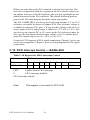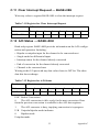
1
PCL-818 Series
12-bit ISA Multifunction Card
User Manual
Copyright
The documentation and the software included with this product are copyrighted 2010 by Advantech Co., Ltd. All rights are reserved. Advantech
Co., Ltd. reserves the right to make improvements in the products
described in this manual at any time without notice. No part of this manual may be reproduced, copied, translated or transmitted in any form or
by any means without the prior written permission of Advantech Co., Ltd.
Information provided in this manual is intended to be accurate and reliable. However, Advantech Co., Ltd. assumes no responsibility for its use,
nor for any infringements of the rights of third parties, which may result
from its use.
Acknowledgements
Intel and Pentium are trademarks of Intel Corporation.
Microsoft Windows and MS-DOS are registered trademarks of
Microsoft Corp.
All other product names or trademarks are properties of their respective
owners.
Part No. 20038180A0
2nd Edition
Printed in Taiwan
January 2010
PCL-818 Series User Manual
ii
Product Warranty (2 years)
Advantech warrants to you, the original purchaser, that each of its products will be free from defects in materials and workmanship for two years
from the date of purchase.
This warranty does not apply to any products which have been repaired or
altered by persons other than repair personnel authorized by Advantech,
or which have been subject to misuse, abuse, accident or improper installation. Advantech assumes no liability under the terms of this warranty as
a consequence of such events.
Because of Advantech’s high quality-control standards and rigorous testing, most of our customers never need to use our repair service. If an
Advantech product is defective, it will be repaired or replaced at no
charge during the warranty period. For out-of-warranty repairs, you will
be billed according to the cost of replacement materials, service time and
freight. Please consult your dealer for more details.
If you think you have a defective product, follow these steps:
1.
Collect all the information about the problem encountered. (For
example, CPU speed, Advantech products used, other hardware
and software used, etc.) Note anything abnormal and list any
onscreen messages you get when the problem occurs.
2.
Call your dealer and describe the problem. Please have your manual, product, and any helpful information readily available.
3.
If your product is diagnosed as defective, obtain an RMA (return
merchandize authorization) number from your dealer. This allows
us to process your return more quickly.
4.
Carefully pack the defective product, a fully-completed Repair and
Replacement Order Card and a photocopy proof of purchase date
(such as your sales receipt) in a shippable container. A product
returned without proof of the purchase date is not eligible for warranty service.
5.
Write the RMA number visibly on the outside of the package and
ship it prepaid to your dealer.
iii
Declaration of Conformity
CE
This product has passed the CE test for environmental specifications
when shielded cables are used for external wiring. We recommend the use
of shielded cables. This kind of cable is available from Advantech. Please
contact your local supplier for ordering information.
Technical Support and Assistance
Step 1. Visit the Advantech web site at www.advantech.com/support
where you can find the latest information about the product.
Step 2. Contact your distributor, sales representative, or Advantech's customer service center for technical support if you need additional
assistance. Please have the following information ready before
you call:
- Product name and serial number
- Description of your peripheral attachments
- Description of your software (operating system, version, application software, etc.)
- A complete description of the problem
- The exact wording of any error messages
PCL-818 Series User Manual
iv
Safety Instructions
1.
Read these safety instructions carefully.
2.
Keep this User's Manual for later reference.
3.
Disconnect this equipment from any AC outlet before cleaning.
Use a damp cloth. Do not use liquid or spray detergents for cleaning.
4.
For plug-in equipment, the power outlet socket must be located
near the equipment and must be easily accessible.
5.
Keep this equipment away from humidity.
6.
Put this equipment on a reliable surface during installation. Dropping it or letting it fall may cause damage.
7.
The openings on the enclosure are for air convection. Protect the
equipment from overheating. DO NOT COVER THE OPENINGS.
8.
Make sure the voltage of the power source is correct before connecting the equipment to the power outlet.
9.
Position the power cord so that people cannot step on it. Do not
place anything over the power cord.
10.
All cautions and warnings on the equipment should be noted.
11.
If the equipment is not used for a long time, disconnect it from the
power source to avoid damage by transient overvoltage.
12.
Never pour any liquid into an opening. This may cause fire or electrical shock.
13.
Never open the equipment. For safety reasons, the equipment
should be opened only by qualified service personnel.
14.
If one of the following situations arises, get the equipment checked
by service personnel:
a. The power cord or plug is damaged.
b. Liquid has penetrated into the equipment.
c. The equipment has been exposed to moisture.
d. The equipment does not work well, or you cannot get it to work
according to the user's manual.
e. The equipment has been dropped and damaged.
f. The equipment has obvious signs of breakage.
15.
DO NOT LEAVE THIS EQUIPMENT IN AN ENVIRONMENT
WHERE THE STORAGE TEMPERATURE MAY GO BELOW v
20° C (-4° F) OR ABOVE 60° C (140° F). THIS COULD DAMAGE THE EQUIPMENT. THE EQUIPMENT SHOULD BE IN A
CONTROLLED ENVIRONMENT.
16.
CAUTION: DANGER OF EXPLOSION IF BATTERY IS
INCORRECTLY REPLACED. REPLACE ONLY WITH THE
SAME OR EQUIVALENT TYPE RECOMMENDED BY THE
MANUFACTURER, DISCARD USED BATTERIES ACCORDING TO THE MANUFACTURER'S INSTRUCTIONS.
The sound pressure level at the operator's position according to IEC 7041:1982 is no more than 70 dB (A).
DISCLAIMER: This set of instructions is given according to IEC 704-1.
Advantech disclaims all responsibility for the accuracy of any statements
contained herein.
PCL-818 Series User Manual
vi
Contents
Chapter
Chapter
Chapter
1 Overview .......................................................... 2
1.1
1.2
1.3
1.4
Introduction ....................................................................... 2
Features ............................................................................. 3
Applications ...................................................................... 4
Installation Guide .............................................................. 5
1.5
1.6
1.7
Software Overview............................................................ 7
Device Driver Roadmap.................................................... 8
Accessories...................................................................... 10
Figure 1.1:Installation Flow Chart ................................. 6
2 Installation ..................................................... 12
2.1
2.2
Unpacking ....................................................................... 12
Driver Installation .......................................................... 13
2.3
2.4
Hardware Installation ..................................................... 15
Device Setup & Configuration........................................ 16
Figure 2.1:Advantech Automation Software Setup ..... 13
Figure 2.2:Options for Driver Setup ............................ 14
Figure 2.3:Device Manager ......................................... 16
Figure 2.4:Device Settings ........................................... 17
Figure 2.5:Device Name .............................................. 18
Figure 2.6:Test Utility .................................................. 19
3 Signal Connections ........................................ 22
3.1
3.2
Overview ......................................................................... 22
Switch & Jumper Settings ............................................... 22
3.3
Signal Connections.......................................................... 30
3.4
Figure 3.1:Connectors, Jumpers& Switches ................ 22
3.3.1
3.3.2
Pin Assignments .......................................................... 30
I/O Connector Signal Description ................................ 31
Figure 3.2:Analog Output Connections ....................... 34
Field Wiring Considerations ........................................... 36
Appendix A Specifications ................................................. 38
A.1
A.2
A.3
A.4
A.5
Analog Input ................................................................... 38
Analog Output ................................................................. 39
Digital Input /Output ....................................................... 39
Counter/Timer ................................................................. 40
General ............................................................................ 40
Appendix B Block Diagram ............................................... 42
B.1
B.2
PCL-818HD/HG.............................................................. 42
PCL-818L........................................................................ 42
Appendix C Register Structure & Format ....................... 44
C.1
C.2
C.3
Overview ........................................................................ 44
I/O Port Address Map .................................................... 44
A/D Data & Channels — BASE+00H~01H .................. 47
vii
Table of Contents
C.4
C.5
C.6
C.7
C.8
C.9
C.10
C.11
C.12
C.13
C.14
C.15
C.16
C.17
C.18
C.19
Software A/D Trigger — BASE+00H ........................... 48
A/D RangeControl — BASE+01H ................................ 48
MUX Scan Channel Control — BASE+02H.................. 50
MUX Scan Channel Status — BASE+02H .................... 52
Digital I/O Registers - BASE + 03/0BH ......................... 52
D/A Output — BASE+04/05H ....................................... 53
FIFO Interrupt Control — BASE+06H........................... 54
Clear Interrupt Request — BASE+08H .......................... 55
A/D Status — BASE+08H.............................................. 55
A/D Control — BASE+09H ........................................... 57
Timer/Counter Enable — BASE+0AH........................... 59
Programmable Timer/Counter — BASE+0C~0FH ........ 59
Clear FIFO Interrupt Request — BASE+14H ................ 60
A/D Data and Channel from FIFO - BASE + 17/18H .... 60
FIFO Status — BASE+19H ............................................ 61
FIFO Clear — BASE+19H ............................................. 62
Appendix D Calibration ..................................................... 64
D.1
VR Assignment .............................................................. 65
D.2
D.3
A/D Calibration ............................................................... 66
D/A Calibration ............................................................... 66
Figure D.1:PCL-818HD/HG/L VR Assignment ......... 65
PCL-818 Series User Manual
viii
CHAPTER
1
2
Overview
Sections include:
• Introduction
• Features
• Applications
• Installation guide
• Software Overview
• Device Driver Roadmap
• Accessories
Chapter 1 Overview
1.1 Introduction
Thank you for buying the Advantech PCL-818HD/HG/L. The PCL818HD/HG/L is a high-performance multifunction data acquisition card
for IBM PC/XT/AT or compatible computers. It offers the five most
desired measurement and control functions: 12-bit A/D conversion, D/A
conversion, digital input, digital output and timer/counter.
A programmable-gain instrument amplifier (x 0.5, 1, 2, 4 and 8) lets you
acquire different input signals without external signal conditioning. An
onboard 1 K word FIFO buffer provides high-speed data transfer and predictable performance under Windows.
Automatic channel scanning circuitry and on-board SRAM let you perform multiple-channel A/D conversion with DMA and individual gains
for each channel.
The PCL-818HD uses a CPLD chip designed in-house by Advantech
engineers. This single chip integrates most of the card's functions, giving
you maximum accuracy and reliability, along with minimum cost, size
and power consumption.
The PCL-818HD is hardware and software compatible with its popular
predecessor, the PCL-8l8HG. This puts rich software support and a wide
variety of external signal conditioning boards at your disposal.
Note:
AI data acquisition in DMA mode is only recommended
when using an Intel Pentium 3 motherboard. It will not
function properly on a Pentium 4 motherboard or above.
PCL-818 Series User Manual
2
1.2 Features
• 16 single-ended or eight differential analog inputs, switch selectable
• 12-bit A/D, up to 100 KHz sampling rate with DMA transfer and different gain for each channel
• Software-selectable gain: x 0.5, 1, 2, 4 or 8
• Onboard 1 K word FIFO buffer with software selectable interrupt
• Software selectable analog input ranges (VDC):
• Bipolar: +/-0.625, +/-1.25, +/-2.5, +/-5, +/-10
• Unipolar: 0 to 1.25, 0 to 2.5, 0 to 5, 0 to 10
• 16 digital inputs and 16 digital outputs, TTL/DTL compatible
• One 12-bit analog output channel
• Flexible triggering options: software, programmable pacer and external
pulse
• Data transfers by program control, interrupt handler routine or DMA
The PCL-818HD/HG/L offers the following main features:
Automatic Channel/Gain Scanning
The PCL-818HD/HG/L features an automatic channel/gain scanning circuit. This circuit, instead of your software, controls multiplexer switching
during sampling. On-board SRAM stores different gain values for each
channel. This combination lets you perform multi-channel high-speed
sampling (up to 100 KHz) with different gains for each channel and
DMA data transfer.
Wide Selection with Migration Path
The PCL-818HD/HG/L lets you choose the card that exactly matches
your application and price range. The PCL-818HD/HG/L is the perfect
choice if you on a tight budget. It offers the best price/performance in the
market. IF you need more power, you can easily upgrade to any other
card in the series. The PCL-818HD/HG/L is connector compatible. All
your programs will work with your new card, protecting your investment.
3
Chapter 1
Keeping Output Values after System Reset
When the system is hot reset (power not shut down), the PCL-818HD/
HG/L can either retain the last analog output values, or return to its
default configuration, depending on the jumper setting. This practical
function eliminates danger caused by improper operation during unexpected system reset.
Board ID
The PCL-818HD/HG/L has a built-in DIP Switch that helps define each
card’s ID when multiple PCL-818HD/HG/L cards have been installed on
the same PC chassis. The board ID setting function is very useful when
users build their system with multiple PCL-818HD/HG/L cards. With
correct Board ID settings, you can easily identify and access each card
during hardware configuration and software programming.
Note: For detailed specifications of the PCL-818HD/HG/L, please refer
to Appendix A, Specifications.
1.3 Applications
• Transducer and sensor measurements
• Waveform acquisition and analysis
• Process control and monitoring
• Vibration and transient analysis
PCL-818 Series User Manual
4
1.4 Installation Guide
Before you install your PCL-818HD/HG/L card, please make sure you
have the following necessary components:
• PCL-818HD/HG/L DA&C Card
• PCL-818HD/HG/L User’s Manual
• Driver Software Advantech DLL drivers (included in the CD-ROM)
• Wiring Cable
PCL-10120/10137 (option)
• Wiring Board
ADAM-3920/3937, PCLD-7216/780/782/782B/
785/785B/786/788/789D/880/885/8115 (optional)
• PC or workstation with a PCI-bus slot (Win 95/98/NT/2000/ME/XP)
Some other optional components are available for enhanced operation:
• Application software ActiveDAQ, GeniDAQ or 3rd party software
After you get the necessary components and maybe some of the accessories for enhanced operation of your Multifunction card, you can then
begin the Installation procedures. Figure 1-1 on the next page provides a
concise flow chart to give users a broad picture of the software and hardware installation procedures:
5
Chapter 1
Figure 1.1: Installation Flow Chart
PCL-818 Series User Manual
6
1.5 Software Overview
Advantech offers a rich set of DLL drivers, third-party driver support and
application software to help fully exploit the functions of your PCL818HD/HG/L card:
• Device Drivers (on the companion CD-ROM)
• LabVIEW driver
• Advantech ActiveDAQ
• Advantech GeniDAQ
Programming choices for DA&C cards: You may use Advantech application software such as Advantech Device Drivers. On the other hand,
advanced users are allowed another option for register-level programming, although not recommended due to its laborious and time-consuming nature.
Device Drivers
The Advantech Device Drivers software is included on the companion
CD-ROM at no extra charge. It also comes with all the Advantech DA&C
cards. Advantech’s Device Drivers features a complete I/O function
library to help boost your application performance. The Advantech
Device Drivers for Windows 95/98/NT/2000/ME/XP works seamlessly
with development tools such as Visual C++, Visual Basic, Borland C++
Builder and Borland Delphi.
Register-level Programming
Register-level programming is available for experienced programmers
who find it necessary to write code directly at the level of the device register. Since register-level programming requires much effort and time, we
recommend that you use the Advantech Device Drivers instead. However, if register-level programming is indispensable, you should refer to
the relevant information in Appendix C, Register Structure and Format,
or to the example codes included on the companion CD-ROM.
7
Chapter 1
1.6 Device Driver Roadmap
This section will provide you a roadmap to demonstrate how to build an
application from scratch using Advantech Device Drivers with your
favorite development tools such as Visual C++, Visual Basic, Delphi and
C++ Builder. The step-by-step instructions on how to build your own
applications using each development tool will be given in the Device
Drivers Manual. Moreover, a rich set of example source code is also
given for your reference.
Programming Tools
Programmers can develop application programs with their favorite development tools:
• Visual C++
• Visual Basic
• Delphi
• C++ Builder
For instructions on how to begin programming works in each development tool, Advantech offers a Tutorial Chapter in the Device Drivers
Manual for your reference. Please refer to the corresponding sections in
this chapter on the Device Drivers Manual to begin your programming
efforts. You can also look at the example source code provided for each
programming tool, since they can get you very well oriented.
The Device Drivers Manual can be found on the companion CD-ROM.
Alternatively, if you have already installed the Device Drivers on your
system, The Device Drivers Manual can be readily accessed through the
Start button:
Start/Advantech Automation/Device Manager/Device Driver’s Manual
The example source code could be found under the corresponding installation folder such as the default installation path:
\Program Files\Advantech\ADSAPI\Examples
For information about using other function groups or other development
tools, please refer to the Creating Windows 95/NT/2000 Application with
Device Drivers chapter and the Function Overview chapter on the Device
Drivers Manual.
PCL-818 Series User Manual
8
Programming with Device Drivers Function Library
Advantech Device Drivers offer a rich function library that can be utilized in various application programs. This function library consists of
numerous APIs that support many development tools, such as Visual
C++, Visual Basic, Delphi and C++ Builder.
According to their specific functions or services, those APIs can be categorized into several function groups:
• Analog Output Function Group
• Digital Input/Output Function Group
• Counter Function Group
• Port Function Group (direct I/O)
• Event Function Group
For the usage and parameters of each function, please refer to the Function Overview chapter in the Device Drivers Manual.
Troubleshooting Device Drivers Error
Driver functions will return a status code when they are called to perform
a certain task for the application. When a function returns a code that is
not zero, it means the function has failed to perform its designated function. To troubleshoot the Device Drivers error, you can pass the error
code to DRV_GetErrorMessage function to return the error message.
Alternatively, you can refer to the Device Drivers Error Codes Appendix
in the Device Drivers Manual for a detailed listing of Error Codes, Error
IDs and the Error Messages.
9
Chapter 1
1.7 Accessories
Advantech offers a complete set of accessory products to support the
PCL-818HD/HG/L card. These accessories include:
Wiring Cables
• PCL-10120 The PCL-10120 cable is a 20-pin flat cable for PCL818HD/HG/L cards.
• PCL-10137 The PCL-10137 shielded cable is specially designed for
PCL-818HD/HG/L cards to provide high resistance to
noise. To achieve a better signal quality, the signal wires
are twisted in such a way as to form a “twisted-pair cable”,
reducing cross-talk and noise from other signal sources.
Furthermore, its analog and digital lines are separately
sheathed and shielded to neutralize EMI/EMC problems.
Wiring Boards
• ADAM-3920
20-pin wiring terminal for DIN-rail mounting
• ADAM-3937
37-pin D-type wiring terminal for DIN-rail mounting
• PCLD-7216
16-channel SSR I/O module carrier board
• PCLD-780
Universal screw-terminal board
• PCLD-782
16-channel opto-isolated D/I board
• PCLD-782B
24-channel opto-isolated D/I board
• PCLD-785
16-channel relay output board
• PCLD-785B
24-channel relay output board
• PCLD-786
8-channel SSR I/O module carrier board
• PCLD-788
16-channel relay multiplexer board
• PCLD-789D
Amplifier and multiplexer board
• PCLD-880
Universal screw-terminal board
• PCLD-885
16-channel power relay output board
• PCLD-8115
Industrial wiring terminal with CJC circuit
PCL-818 Series User Manual
10
CHAPTER
2
2
Installation
Sections include:
• Unpacking
• Driver Installation
• Hardware Installation
• Device Setup & Configuration
Chapter 2 Installation
2.1 Unpacking
After receiving your PCL-818HD/HG/L package, please inspect its contents first. The package should contain the following items:
• PCL-818HD/HG/L card
• Companion CD-ROM (Device Drivers included)
• User’s Manual
The PCL-818HD/HG/L card harbors certain electronic components vulnerable to electrostatic discharge (ESD). ESD can easily damage the integrated circuits and certain components if preventive measures are
ignored.
Before removing the card from the antistatic plastic bag, you should take
the following precautions to ward off possible ESD damage:
• Touch the metal part of your computer chassis with your hand to discharge the static electricity accumulated on your body. Alternatively,
one can also use a grounding strap.
• Touch the anti-static bag to a metal part of your computer chassis
before opening the bag.
• Take hold of the card only by the metal bracket when removing it out of
the bag.
After taking out the card, you should first:
• Inspect the card for any possible signs of external damage (loose or
damaged components, etc.). If the card is visibly damaged, please
notify our service department or our local sales representative immediately. Do not install a damaged card into your system.
Note:
Keep the anti-static bag for future use. You might
need the original bag to store the card if you
have to remove the card from PC or transport it
elsewhere.
PCL-818 Series User Manual
12
2.2 Driver Installation
We recommend you to install the driver before you install the PCL818HD/HG/L card into your system, since this will guarantee a smooth
installation process.
The Advantech Device Drivers Setup program for the PCL-818HD/HG/L
card is included in the companion CD-ROM that is shipped with your
DA&C card package. Please follow the steps below to install the driver
software:
Step 1: Insert the companion CD-ROM into your CD-ROM drive.
Step 2: The Setup program will be launched automatically if you have the
autoplay function enabled on your system. When the Setup Program is launched, you will see the following Setup Screen.
Note:
If the autoplay function is not enabled on your
computer, use Windows Explorer or Windows
Run command to execute SETUP.EXE on the
companion CD-ROM.
Figure 2.1: Advantech Automation Software Setup
13
Chapter 2
Step 3: Select the Device Drivers option.
Step 4: Select the specific device then just follow the installation
instructions step by step to complete your device driver installation and setup.
Figure 2.2: Options for Driver Setup
For further information on driver-related issues, an online version of the
Device Drivers Manual is available by accessing the following path:
Start/Advantech Automation/Device Manager/Device Driver’s Manual
PCL-818 Series User Manual
14
2.3 Hardware Installation
Note:
Make sure you have installed the driver first before you
install the card (please refer to 2.2 Driver Installation)
After the Device Drivers installation is completed, you can then install
the PCL-818HD/HG/L card into any PCI slot on your computer. However, it is suggested that you refer to the computer user’s manual or
related documentation if you have any doubt. Please follow the steps
below to install the card onto your system.
Step 1: Turn off your computer and unplug the power cord and cables.
TURN OFF your computer before installing or removing any
components on the computer.
Step 2: Remove the cover of your computer.
Step 3: Remove the slot cover on the back panel of your computer.
Step 4: Touch the metal part on the surface of your computer to neutralize
the static electricity that might be on your body.
Step 5: Insert the PCL-818HD/HG/L card into an ISA slot. Hold the card
only by its edges and carefully align it with the slot. Insert the card
firmly into place. Use of excessive force must be avoided; otherwise, the card might be damaged.
Step 6: Fasten the bracket of the ISA card on the back panel rail of the
computer with screws.
Step 7: Connect appropriate accessories (37-pin cable, wiring terminals,
etc. if necessary) to the ISA card.
Step 8: Replace the cover of your computer chassis. Reconnect the cables
you removed in step 2.
Step 9: Plug in the power cord and turn on the computer.
After your card is properly installed on your system, you can now configure your device using the Advantech Device Manager Program that has
itself already been installed on your system during driver setup. A complete device installation procedure should include device setup, configuration and testing. The following sections will guide you through the
Setup, Configuration and Testing of your device.
15
Chapter 2
2.4 Device Setup & Configuration
The Advantech Device Manager program is a utility that allows you to set
up, configure and test your device, and later stores your settings on the
system registry. These settings will be used when you call the APIs of
Advantech Device Drivers.
Setting Up the Device
Step 1:To install the I/O device for your card, you must first run the
Device Installation program (by accessing Start/Advantech Automation/Device Manager/Advantech Device Manager ).
Step 2:You can then view the device(s) already installed on your system
(if any) on the Installed Devices list box. Since you have not
installed any device yet, you might see a blank list such as the one
below (Fig. 2-3).
Figure 2.3: Device Manager
PCL-818 Series User Manual
16
Step 3:Scroll down the List of Devices box to find the device that you
wish to install, then click the Add… button. You will see a Device
Setting dialog box such as the one in Fig. 2-4.
Configuring the Device
Step 4:On the Device Setting dialog box (Fig. 2-4), you can configure the
A/D channels configuration either as 8 Differential or 16 Singleended, and specify the D/A voltage reference either as External or
Internal.
Figure 2.4: Device Settings
Step 5:After you have finished configuring the device, click OK and the
device name will appear in the Installed Devices box as seen
below:
17
Chapter 2
Figure 2.5: Device Name
After your card is properly installed and configured, you can click the
Test… button to test your hardware by using the testing utility supplied.
PCL-818 Series User Manual
18
Figure 2.6: Test Utility
For more detailed information, please refer to Chapter 2 of the Device
Drivers Manual. You can also find the rich examples on the CD-ROM to
speed up your programming.
19
Chapter 2
PCL-818 Series User Manual
20
CHAPTER
3
2
Signal Connections
Sections include:
• Overview
• Switch & Jumper Settings
• Signal Connections
• Field Wiring Considerations
Chapter 3 Signal Connections
3.1 Overview
Maintaining signal connections is one of the most important factors in
ensuring that your application system is sending and receiving data correctly. A good signal connection can avoid unnecessary and costly damage to your PC and other hardware devices. This chapter provides useful
information about how to connect input and output signals to the PCL818HD/HG/L via the I/O connector.
3.2 Switch & Jumper Settings
The PCL-818HD/HG/L card has one function switch and five jumper settings.
Figure 3.1: Connectors, Jumpers& Switches
PCL-818 Series User Manual
22
Base Address Selection (SW1)
You control the PCL-818HD/HG/L's operation by reading or writing data
to the PC's I/O (input/output) port addresses. The PCL-818HD/HG/L
requires 32 consecutive address locations with the FIFO buffer enabled or
16 locations with the FIFO disabled.
Switch SW1 sets the card's base (beginning) address. Valid base
addresses range from Hex 000 to Hex 3F0. Other devices in your system
may, however, be using some of these addresses.
We set the PCL-818HD/HG/L for a base address of Hex 300 at the factory. If you need to adjust it to some other address range, set switch SW1
as shown in the following table:
Note:
Switches 1-6 control the PC bus address lines as
follows:
Switch
1
2
3
4
5
6
Line
A9
A8
A7
A6
A5
A4
23
Chapter 3
Channel Configuration, S/E or DIFF (SW2)
The PCL-818HD/HG/L offers 16 single-ended or eight differential analog input channels. Slide switch SW2 changes the channels between single-ended or differential input. Slide the switch to the left-hand position,
marked DIFF, for eight differential inputs (the default) or to the righthand position, marked S/E, for 16 single-ended inputs.
Table 3-1: Switch SW2 Settings
Switches
Function Description
Differential (default)
SW2
Single-ended
DMA Channel Selection (JP7)
The PCL-818HD/HG/L supports DMA data transfer. Jumper JP7 selects
the DMA channel 1 or 3.
Table 3-2: Jumper JP7 Settings
Jumpers
Function Description
Channel 3 (default)
JP7
Channel 1
D/A Reference Voltage, Int./Ext. (JP11)
Jumper JP11 selects reference voltage source for the PCL-818HD/HG/L's
D/A converters. You can use the card's internal reference or supply an
external reference.
PCL-818 Series User Manual
24
Table 3-3: Jumper JP11 Settings
Jumpers
Function Description
JP11
External
Internal (default)
When you set JPI1 to INT, the D/A converter takes its reference voltage
input from the card's on-board reference. Jumper JP10 selects either -5 V
or -10 V on-board reference voltage. With JP11 set to INT the D/A channel has an output range of 0 to +5 V or 0 to +10 V, respectively.
When you set JP11 to EXT, the D/A converter takes its reference voltage
input from pin 31 of connector CN3.You can apply any voltage between 10 V and +10 V to this pin to function as the external reference. The reference input can be either DC or AC (<100 KHz).
When you use an external reference with voltage Vref you can program
the D/A channel to output from 0 V to -Vref, you can also use the D/A
converter as a programmable attenuator. The attenuation factor between
reference input and analog output is:
Attenuation factor = G / 4095
Where G is a value you write to the D/A registers between 0 and 4095.
For example, if you set G to 2048, then the attenuation factor is 0.5. A
sine wave of 10 V amplitude applied to the reference input will generate a
sine wave of 5 V amplitude on the analog output.
25
Chapter 3
Internal Voltage Reference, -10 V or -5 V (JP10)
If you use an internal reference voltage (set with JP11), the PCL-818HD/
HG/L provides a choice of DC internal reference voltage sources: -5 V
and -10 V.
Table 3-4: Jumper JP10 Settings
Jumpers
Function Description
JP10
5 V (default)
10 V
Timer Clock Selection (JP8)
The PCL-818HD/HG/L’s JP8 controls the input clock frequency for the
8254 programmable clock/timer. You have two choices: 10 MHz and 1
MHz. This lets you generate pacer output frequencies from 2.5 MHz to
0.00023 Hz (71 minutes/pulse).
The following equation gives the pacer rate:
Pacer rate = Fclk / (Divl * Div2)
Fclk is 1 MHz or 10 MHz, as set by jumper JP8. Div l and Div2 are the
dividers set in counter 1 and counter 2 in the 8254. See Chapter 8 for
more details.
Table 3-5: Jumper JP8 Settings
Jumpers
Function Description
JP8
1 MHz (default)
10 MHz
PCL-818 Series User Manual
26
FIFO Enable/Disable (JP6)
When you enable the PCL-818HD/HG 's FIFO (First In First Out) buffer,
each time the card makes an A/D reading, it will store the data in both the
A/D output registers (accessed at addresses BASE+0/1) and in the FIFO
buffer (accessed at BASE+23/24). When you enable the FIFO, the PCL818HD/HG will require 32 consecutive I/O addresses.
When you disable the FIFO buffer, you can only access the converted
data from the A/D output registers at BASE+O/1. The PCL-818HD/HG
will only require 16 consecutive VO addresses.
Table 3-6: Jumper JP6 Settings
Jumpers
Function Description
JP6
Disabled
Enabled (default)
Ext. Trigger and Counter Gate 0 Control (JP5)
JP5 has two jumpers. The upper jumper selects the card's A/D trigger
source when you use external triggering. The lower jumper selects the
gate control for counter 0 of the card's 8254 timer/counter.
Table 3-7: Jumper Settings
Jumpers
Function Description
JP5 (Upper)
G0 (default)
DI2
JP5 (Lower)
Ext. (default)
DI0
27
Chapter 3
We recommend that you leave JP5 set to the default DIO and DI2,
because the software driver requires this setting.
FIFO Interrupt Selection (JP9)
The PCL-818HD/HG’s JP9 controls the interrupt (2 through 7) that the
FIFO generates when it is half full. The FIFO interrupt control register,
BASE+6, enables and disables this interrupt. Jumper settings are as follows:
FIFO IRQ Select (IRQ2 Default)
Digital Output, 20-pin or 37-pin Connector (JP1-4)
The PCL-818HD/L’s JPI to JP4 switch digital output channels O to 3
between the card's 20-pin connector and 37-pin connector. If you set the
jumpers to the left (D) side, the digital output signals will come out on
connector CN1 (20-pin). If you set the jumpers to the right (S) side, the
output signals will come out on connector CN3 (37-pin).
These four digital output signals select the analog input channel when
you use a multiplexer/amplifier daughter board. Daughter boards with a
DB-37 connector, such as the PCLD-789D, read the digital output signals
from the DB-37 connector (CN3). With other daughter boards you will
need to connect an external 20-pin flat cable from CN1 to the daughter
board.
PCL-818 Series User Manual
28
Table 3-8: Jumper Settings
Jumpers
Function Description
JP1 (first)
S0
D0 (default)
JP1 (second)
S1
D1 (default)
JP1 (third)
S2
D2 (default)
JP1 (fourth)
S3
D3 (default)
29
Chapter 3
3.3 Signal Connections
3.3.1 Pin Assignments
Figure 3-2 shows the pin assignments for the 37-pin I/O connector.
D/O 0
D/O 2
D/O 4
D/O 6
D/O 8
D/O 10
D/O 12
D/O 14
D.GND
+5 V
CN1
1
3
5
7
9
11
13
15
17
19
2
4
6
8
10
12
14
16
18
20
D/O 1
D/O 3
D/O 5
D/O 7
D/O 9
D/O 11
D/O 13
D/O 15
D.GND
+12 V
D/I 0
D/I 2
D/I 4
D/I 6
D/I 8
D/I 10
D/I 12
D/I 14
D.GND
+5 V
CN3 (Single ended)
A/D S0
A/D S1
A/D S2
A/D S3
A/D S4
A/D S5
A/D S6
A/D S7
A.GND
A.GND
VREF
S0*
+12 V
S2*
D.GND
NC
Counter 0 CLK
Counter 0 OUT
+5 V
1
2
3
4
5
6
7
8
9
10
11
12
13
14
15
16
17
18
19
CN2
1
3
5
7
9
11
13
15
17
19
2
4
6
8
10
12
14
16
18
20
D/I 1
D/I 3
D/I 5
D/I 7
D/I 9
D/I 11
D/I 13
D/I 15
D.GND
+12 V
CN3 (Differential)
20
21
22
23
24
25
26
27
28
29
30
31
32
33
34
35
36
37
A/D S8
A/D S9
A/D S10
A/D S11
A/D S12
A/D S13
A/D S14
A/D S15
A.GND
A.GND
DA0.OUT
DA0.VREF
S1*
S3*
D.GND
EXT.TRIG
Counter 0 GATE
PACER
A/D H0
A/D H1
A/D H2
A/D H3
A/D H4
A/D H5
A/D H6
A/D H7
A.GND
A.GND
VREF
S0*
+12 V
S2*
D.GND
NC
Counter 0 CLK
Counter 0 OUT
+5 V
.
1
2
3
4
5
6
7
8
9
10
11
12
13
14
15
16
17
18
19
20
21
22
23
24
25
26
27
28
29
30
31
32
33
34
35
36
37
A/D L0
A/D L1
A/D L2
A/D L3
A/D L4
A/D L5
A/D L6
A/D L7
A.GND
A.GND
DA0.OUT
DA0.VREF
S1*
S3*
D.GND
EXT.TRIG
Counter 0 GATE
PACER
.
Note: The S0/S1 is NC, and S2/S3 is AGND for PCL-818HG
PCL-818 Series User Manual
30
3.3.2 I/O Connector Signal Description
Table 3-9 I/O Connector Signal Descriptions
Signal Name Reference Direction Description
A/D S <0..15> A.GND
Input
Analog input (single-ended), channels 0 through
15.
A/D H <0..7> A.GND
Input
Analog input high (differential), channels 0
through 7.
A/D L <0..7>
A.GND
Input
Analog input low (differential), channels 0 through
7.
D/A
A.GND
Output
Analog output
AGND
Analog Ground. The two ground references
(A.GND and D.GND) are connected together on
the PCL-818HD/HG/L card.
D/O
D.GND
Output
Digital output, channels 0 through 15.
D/I
D.GND
Input
Digital input, channels 0 through 15.
CLK
D.GND
Input
Clock input for the 8254.
GATE
D.GND
Input
Gate input for the 8254.
OUT
D.GND
Output
Signal output for the 8254.
VREF
D.GND
Output
Voltage reference.
REFIN
D.GND
Input
External voltage reference input.
S1-S4
D.GND
Output
Daughterboard channel select.
DGND
Digital Ground. The two ground references
(A.GND and D.GND) are connected together on
the PCL-818HD/HG/L card.
+12V
D.GND
Output
+12 VDC Source (from ISA bus directly with FUSE
protection).
+5V
D.GND
Output
+5 VDC Source (from ISA bus directly with FUSE
protection).
NC
No connection.
Analog Input Connection
The PCL-818HD/HG/L supports either 16 single-ended or 8 differential
analog inputs. Switch SW2 selects the input channel configuration.
Single-ended Channel Connections
Single-ended connections use only one signal wire per channel. The voltage on the line references to the common ground on the card. A signal
source without a local ground is called a "floating" source. It is fairly simple to connect a single ended channel to a floating signal source. A standard wiring diagram looks like this:
S ign al In p ut
+
Vs
-
T o A /D
A .G N D
A .G N D
31
Chapter 3
Differential Channel Connections
Differential input connections use two signal wires per channel. The card
measures only the voltage difference between these two wires, the HI
wire and the LOW wire. If the signal source has no connection to ground,
it is called a "floating" source. A connection must exist between LOW
and ground to define a common reference point for floating signal
sources. To measure a floating sources connect the input channels as
shown below:
HIGH
+
+
Vs
-
LO W
+
Vin
-
A.GND
If the signal source has one side connected to a local ground, the signal
source ground and the PCL-818HD/HG/L ground will not be at exactly
the same voltage, as they are connected through the ground return of the
equipment and building wiring. The difference between the ground voltages forms a common-mode voltage.
To avoid the ground loop noise effect caused by common-mode voltages,
connect the signal ground to the LOW input. Do not connect the LOW
input to the PCL-818HD/HG/L ground directly. In some cases you may
also need a wire connection between the PCL-818HD/HG/L ground and
the signal source ground for better grounding. The following two diagrams show correct and incorrect connections for a differential input with
local ground:
PCL-818 Series User Manual
32
Correct Connection
HIGH
+
+
Vs
-
LOW
+
Vin
-
Vin=Vs
-
- +
Vcm
GND
Incorrect Connection
HIGH
+
+
Vs
-
+
Vin
-
Vin=Vs+Vcm
LOW
- +
-
Vcm
GND
Expanding Analog Inputs
You can expand any or all of the PCL-818HD/HG/L's A/D input channels
using multiplexing daughterboards. Daughterboards without D-type connectors require the PCLD-774 Analog Expansion Board.
The PCLD-789(D) Amplifier and Multiplexer multiplexes 16 differential
inputs to one A/D input channel. You can cascade up to eight PCLD789(D)s to the PCL-818HD/HG/L for a total of 128 channels. See the
PCLD-789(D) user's manual for complete operating instructions.
The PCLD-774 Analog Expansion Board accommodates multiple external signal-conditioning daughter boards, such as PCLD-779 and PCLD789(D). It features five sets of on-board 20-pin header connectors. A special star-type architecture lets you cascade multiple signal-conditioning
boards without the signal-attenuation and current-loading problems of
normal cascading.
33
Chapter 3
The PCLD-8115 Screw Terminal Board makes wiring connections easy.
It provides 20-pin flat cable and DB-37 cable connectors. It also includes
CJC (Cold Junction Compensation) circuits.
Special circuit pads on the PCLD-8115 accommodate passive signal conditioning components. You can easily implement a low-pass filter, attenuator or current shunt by adding resistors and capacitors.
Analog Output Connection
The PCL-818HD/HG/L provides one D/A output channel. You can use
the internal precision -5 V or -10 V reference to generate 0 to +5 V or 0 to
+10 V D/A output. Use an external reference for other D/A output ranges.
The maximum reference input voltage is ±10 V and maximum output
scaling is ±10 V. Loading current for D/A outputs should not exceed 5
mA.
Connector CN3 provides D/A signals. Important D/A signal connections
such as input reference, D/A outputs and analog ground appear below:
CN3-31 D/A REF IN
D/A
CN3-30 D/A OUT
CN3-9,10,28,29 A.GND
JP11
ON-Board
-5V
REF
CN3-11 VREF
-10V
JP10
Figure 3.2: Analog Output Connections
PCL-818 Series User Manual
34
Digital Signal Connections
The PCL-818HD/HG/L has 16 digital input and 16 digital output channels. The digital I/O levels are TTL compatible. The following figure
shows connections to exchange digital signals with other TTL devices:
TTL Devices
DO
DI
D.GND D.GND
To receive an OPEN/SHORT signal from a switch or relay, add a pull-up
resistor to ensure that the input is held at a high level when the contacts
are open. See the figure below:
+5V
4.7K
D.GND
35
Chapter 3
3.4 Field Wiring Considerations
When you use the PCL-818HD/HG/L to acquire data from outside, noises
in the environment might significantly affect the accuracy of your measurements if due cautions are not taken. The following measures will be
helpful to reduce possible interference running signal wires between signal sources and the PCL-818HD/HG/L.
The signal cables must be kept away from strong electromagnetic sources
such as power lines, large electric motors, circuit breakers or welding
machines, since they may cause strong electromagnetic interference.
Keep the analog signal cables away from any video monitor, since it can
significantly affect a data acquisition system.
If the cable travels through an area with significant electromagnetic interference, you should adopt individually shielded, twisted-pair wires as the
analog input cable. This type of cable has its signal wires twisted together
and shielded with a metal mesh. The metal mesh should only be connected to one point at the signal source ground.
Avoid running the signal cables through any conduit that might have
power lines in it.
If you have to place your signal cable parallel to a power line that has a
high voltage or high current running through it, try to keep a safe distance
between them. Alternatively, you can place the signal cable at a right
angle to the power line to minimize the undesirable effect.
The signals transmitted on the cable will be directly affected by the quality of the cable. In order to ensure better signal quality, we recommend
that you use the PCL-10137 shielded cable.
PCL-818 Series User Manual
36
APPENDIX
A
2
Specifications
Appendix A Specifications
A.1 Analog Input
Channels
16 single-ended or 8 differential or combination
Resolution
12-bit
FIFO Size
4K samples (for PCL-818HD/HG only)
PCL-818HD Max. Sam- 100 KS/s
pling Rate1
PCL-818HG Max. Sam- Gain
0.5, 1
5, 10
50, 100 500, 1000
pling Rate
Speed
100 KS/s 35 KS/s 7 KS/s 770 S/s
PCL-818L Max. Sam- 40 KS/s
pling Rate1
Conversion Time
8 µs
Input range and
Gain
0.5
1
2
4
8
Gain List for PCLUnipolar
N/A
0~10
0~5
0~2.5
0~1.25
818HD
Bipolar
±10
±5
±2.5
±1.25
±0.625
Input range and
Gain
0.5 1
5
10 50 100 500 1000
Gain List for PCLUnipolar
N/A 0~1 N/A 0~1 N/A 0~0. N/A 0~0.
818HG
0
1
01
Bipolar
±10 ±5 ±1 ±0.5 ±0.1 ±0.0 ±0.01 ±0.00
5
5
Input range and
Gain
0.5
1
2
4
8
Gain List for PCL-818L Bipolar
±10
±5
±2.5
±1.25
±0.625
Drift
Gain
1
2
4
8
16
Zero (V/)
15
15
15
15
15
Gain (ppm//)
25
25
25
30
40
Small Signal Bandwidth
Gain
1
2
4
8
16
for PGA
Bandwidth
4.0
2.0 MHz 1.5 MHz 0.65
0.35 MHz
Common mode voltage
Max. Input voltage
Input Protect
Input Impedance
Trigger Mode
PCL-818HD/L
Accuracy
PCL-818HG
Accuracy
External TTL Trigger
Input
±11 V max. (operational)
±15 V
30 Vp-p
1 G/5 pF
Software, onboard Programmable Pacer or External
DC
INLE: ±1 LSB
Monotonicity: 12 bits
Offset error: Adjustable to zero
Gain 0.5
1
2
4
Gain error 0.01 0.01
0.02
0.02
(% FSR)
Ch Type S.E./D S.E./D
S.E./D
D
AC
SNR: 68 dB
ENOB: 11 bits
DC
INLE: ±1 LSB
Monotonicity: 12 bits
Offset error: Adjustable to zero
Gain 0.5,1 5,10
50,100 500
Gain error 0.01 0.02
0.04
0.08
(% FSR)
Ch Type S.E./D S.E./D
D
D
AC
SNR: 68 dB
ENOB: 11 bits
Low 0.4 V max.
High 2.4 V min.
PCL-818 Series User Manual
38
8
0.04
D
1000
0.08
D
A.2 Analog Output
Channels
Resolution
Output Range
(Internal & External
Reference)
1
12-bit
Using Internal Reference
0 ~ +5V, 0 ~ +10 V
Using External Reference
-10V ~ +10 V
Accuracy
Relative
Differential
Non-linearity
Adjustable to zero
10V/s
40 ppm/
3 mA
100 K samples/s
0.81 (min.)
5 MHz
26s (to ±1/2 LSB of FSR)
Internal
External
±0.5 LSB
±0.5 LSB (monotonic)
Gain Error
Slew Rate
Drift
Driving Capability
Max. Update Rate
Output Impedance
Digital Rate
Settling Time
Reference Voltage
-5 V ~ + 5 V
-10 V ~ + 10 V
A.3 Digital Input /Output
Input Channels
Level
Input Voltage
Output Channels
Level
Output Voltage
16 bits
TTL compatible
Low
High
16 bits
TTL compatible
Low
High
0.8 V max.
2.0 V min.
0.5 V max. @ +8 mA (sink)
2.4 V min. @ -0.4 mA (source)
39
Appendix A
A.4 Counter/Timer
Device
Channels
Compatibility
Base Clock
Pacer output
Intel 8254 or equivalent
3 channels, 16 bits. 2 channels are permanently configured as programmable pacers; 1 channel is free for your application
TTL/CMOS
Channel 2: Takes input from output of channel 1
Channel 1: 10 MHz or 1MHz, switch selectable
Channel 0: Internal 100 KHz or external clock (10 MHz max.),
selected by software
0.00023 Hz (71 minutes/pulse) to 2.5 MHz
A.5 General
I/O Connector Type
DB-37 female x 1, 20-pin connector x 2
Dimensions
185 mm x 100 mm (7.3" x 3.9")
Power Consumption
Typical
+5 V @ 650 mA
Temperature
Max.
Operation
+5 V @ 700 mA
0 ~ 60 °C (32 ~158°F) (refer to IEC 68-2-1,2)
Relative Humidity
Storage
-20~85°C (-4~185°F)
5~95%RH non-condensing (refer to IEC 68-2-3)
Certification
CE certified
PCL-818 Series User Manual
40
APPENDIX
B
2
Block Diagram
Appendix B Block Diagram
B.1 PCL-818HD/HG
8254
Counter 0 C LK
Counter G ate
Counter # 0
10M Hz
O SC
Divider
Address Bus
Address
Decoder
:
1MHz
10MHz
CLK 1
CLK 2
Counter # 1
Counter # 2
O ut 1
O ut 2
CPLD
100KHz
R egister
Select
12-bit D/A
Converter
Status
PC BUS
Data
Buffer
Interm al Data Bus
DM A Signals
:
Digital
Input
16-bit
Digital O ut
:
Digital
Output
Trigger
Logic
DMA
Logic
Data
MU X
IR Q Signals
D/A O utput
16-bit
Digital In
Channel
Scan Logic
RAM
IR Q
Logic
1 K W ord
FIFO
Sam ple
& H old
:.
Analog
Input
Prog. Gain
Amplifer
EOC
12-bit A/D
C onverter
Ext Trig
MUX
16 S/E
or
8 Diff
Control/Status
Logic
B.2 PCL-818L
8254
C o u n te r 0 C L K
C o u n ter G a te
C o u n te r # 0
10M H z
O SC
D iv id e r
A d d re s s B u s
A d d re s s
D ecoder
:
1MHz
10MHz
CLK 1
CLK 2
C o u n te r # 1
C o u n te r # 2
Out 1
Out 2
CPLD
100KH z
R e g is te r
S e le c t
12 -b it D /A
C o n v erter
S ta tu s
PC BUS
D a ta
B u ffe r
D M A S ig n a ls
:
D ig ital
In p u t
1 6-b it
D igita l O u t
:
D ig ital
O u tp u t
T rig g e r
L o g ic
DMA
L o g ic
D a ta
MUX
RAM
C hannel
S c a n L o g ic
IR Q
L o g ic
EOC
IR Q S ig n a ls
In te rm a l D a ta B u s
D /A O u tp u t
1 6-b it
D ig ital In
PCL-818 Series User Manual
1 2 -b it A /D C o n v e rte r
w ith
S a m p le a n d H o ld
P ro g . G a in
A m p life r
42
E xt T rig
MUX
1 6 S /E
or
8 D iff.
:.
A n alo g
In p u t
C
APPENDIX
2
Register Structure &
Format
Appendix C Register Structure & Format
C.1 Overview
The PCL-818HD/HG/L is delivered with an easy-to-use 32-bit Device
Drivers for user programming under the Windows 95/98/NT/2000/ME/
XP operating system. We advise users to program the PCL-818HD/HG/L
using the 32-bit Device Drivers provided by Advantech to avoid the complexity of low-level registry programming.
The most important consideration in programming the PCL-818HD/HG/
L the register level is to understand the function of the card's registers.
The information in the following sections is provided only for users who
would like to do their own low-level programming.
C.2 I/O Port Address Map
The PCL-818HD/HG/L requires 32 consecutive addresses in the PC's I/O
space. The address of each register is specified as an offset from the card's
base address. For example, BASE+0 is the card's base address and
BASE+7 is the base address plus seven bytes.
Table C-1 shows the function of each register of the PCL-818HD/HG/L
or driver and its address relative to the card's base address.
PCL-818 Series User Manual
44
Table C-1 PCL-818HD/HG/L Register Format (Part 1)
Base Addr.
+HEX
00H R
W
01H
R
W
02H
R
W
03H
R
W
04H
R
W
05H
6
5
4
A/D high byte data and channels
AD11 AD10 AD9
AD8 AD7
A/D range control
G3
MUX scan channel status
CC3
MUX scan channel control
CH3 CH2
CH1
CH0 CL3
Digital Input (low byte)
DI7
DI6
DI5
DI4
DI3
Digital Output (low byte)
DO7 DO6 DO5
DO4 DO3
N/A
DA0
DA8
R
D/A output data
DA11 DA10 DA9
N/A
W
FIFO interrupt control
R
N/A
W
N/A
R
3
A/D low byte data and channels
AD3 AD2
AD1
AD0 C3
Software A/D trigger
D/A output data
DA3 DA2
DA1
N/A
W
06H
7
DA7
2
1
0
C2
C1
C0
AD6
AD5
AD4
G2
G1
G0
CC2
CC1
CC0
CL2
CL1
CL0
DI2
DI1
DI0
DO2
DO1
DO0
DA6
DA5
DA4
FINT
07H
45
Appendix C
Table C-1 PCL-818HD/HG/L Register Format (Part 2)
Base Addr.
+HEX
08H
R
W
09H
R
0BH
0DH
0EH
0FH
5
A/D Status
EOC
U/B
MUX
Clear interrupt request
R
W
Timer/Counter Control
4
3
2
1
0
INT
CN3
CN2
CN1
CN0
I1
I0
DMAE ST1
ST0
I1
I0
DMAE ST1
ST0
TC0
R
TC1
Digital Input (high byte)
DI15
DI14
DI13 DI12 DI11 DI10 DI9
Digital Output (high byte)
DO15 DO14 DO13 DO12 DO11 DO10 DO9
Counter 0
W
Counter 0
R
Counter 1
W
Counter 1
R
Counter 2
W
Counter 2
R
N/A
W
Counter Control
R
W
0CH
6
A/D Control
INTE
I2
A/D Control
INTE
I2
N/A
W
0AH
7
PCL-818 Series User Manual
46
DI8
DO8
Table C-1 PCL-818HD/HG/L Register Format (Part 3)
Base Addr.
+HEX
14H
R
17H
19H
6
5
4
3
2
1
0
N/A
W
Clear FIFO Interrupt Request
R
A/D data and channels from FIFO
AD3
AD2
AD1
AD0 C3
N/A
C2
C1
C0
AD6
AD5
AD4
W
A/D data and channels from FIFO
AD11 AD10 AD9
AD8 AD7
N/A
R
FIFO status
W
FIFO clear
FF
HF
EF
W
18H
7
R
C.3 A/D Data & Channels — BASE+00H~01H
Table C-2 Register for A/D Data & Channels
Read
Bit #
BASE + 00H
BASE + 01H
A/D Data & Channels
7
6
5
AD3
AD2
AD1
AD11 AD10 AD9
4
AD0
AD8
3
C3
AD7
2
C2
AD6
1
C1
AD5
0
C0
AD4
AD11 ~ AD0 Analog to digital data
AD0
the least significant bit (LSB) of the A/D data
AD11
the most significant bit (MSB)
C3 ~ C0
A/D channel number from which the data is derived
C0
the least significant bit (LSB) of the channels
C3
the most significant bit (MSB)
47
Appendix C
C.4 Software A/D Trigger — BASE+00H
You can trigger an A/D conversion from software, the card's on-board
pacer or an external pulse. If you select software triggering, a write to the
register BASE+00H with any value will trigger an A/D conversion.
Bits 1 and 0 of register BASE+09H select the trigger source. See pages
57 and 58 for BASE+09H register layout and programming information.
Table C-3 Register for Software A/D Trigger
Write
Bit #
BASE + 00H
Software A/D trigger
7
6
5
4
X
X
X
X
3
X
2
X
1
X
0
X
C.5 A/D RangeControl — BASE+01H
Each A/D channel has its own individual input range, controlled by a
range code stored in on-board RAM. If you want to change the range
code for a given channel, select the channel as the start channel in register
BASE+02H, MUX scan (described in the next section), then write the
range code to bits 0 to 3 of BASE+01H.
Table C-4 Register for A/D Range Control
Write
Bit #
BASE + 01H
A/D range control
7
6
5
4
X
X
X
X
3
G3*
2
G2*
1
G1
G3 ~ G0
A/D range control
G0
the least significant bit (LSB) of the A/D range
G3
the most significant bit (MSB)
PCL-818 Series User Manual
48
0
G0
Range codes appear below:
PCL-818HD
Input Range (V)
-5 to +5
-2.5 to +2.5
-1.25 to +1.25
-0.625 to +0.625
0 to 10V
0 to 5V
0 to 2.5V
0 to 1.25V
-10V to +10V
N/A
N/A
N/A
N/A
N/A
N/A
N/A
PCL-818HG
Input Range (V)
±5V
±0.5V
±0.05V
±0.005V
0 to 10V
0 to 1V
0 to 0.1V
0 to 0.01V
±10V
±1V
±0.1V
±0.01V
N/A
N/A
N/A
N/A
Unipolar/Bipolar
B
B
B
B
U
U
U
U
B
Unipolar/Bipolar
B
B
B
B
U
U
U
U
B
B
B
B
49
Gain Code
G3
G2
0
0
0
0
0
0
0
0
0
1
0
1
0
1
0
1
1
0
1
0
1
0
1
0
1
1
1
1
1
1
1
1
G1
0
0
1
1
0
0
1
1
0
0
1
1
0
0
1
1
G0
0
1
0
1
0
1
0
1
0
1
0
1
0
1
0
1
Gain Code
G3
G2
0
0
0
0
0
0
0
0
0
1
0
1
0
1
0
1
1
0
1
0
1
0
1
0
1
1
1
1
1
1
1
1
G1
0
0
1
1
0
0
1
1
0
0
1
1
0
0
1
1
G0
0
1
0
1
0
1
0
1
0
1
0
1
0
1
0
1
Appendix C
PCL-818L
Input Range
JP7=5V
±5V
±2.5V
±1.25V
±0.625V
Note:
Range Code
G1
0
0
1
1
JP7=10V
±10V
±5V
±2.5V
±1.25V
G0
0
1
0
1
G3 and G2 are not used for PCL-818L.
C.6 MUX Scan Channel Control — BASE+02H
The write register at BASE+02H controls multiplexer (MUX) scanning.
The high nibble provides the stop scan channel number, and the low nibble provides the start scan channel number. Writing to this register automatically initializes the MUX to the start channel. Each A/D conversion
trigger sets the MUX to the next channel.
With continuous triggering the MUX will scan from the start channel to
the end channel, then repeat. For example, if the start channel is 3 and the
stop channel is 7, then the scan sequence is 3, 4, 5, 6, 7, 3, 4, 5, 6, 7, 3,
4.…
PCL-818 Series User Manual
50
Table C-5 Register for MUX Scan Channel Control
Write
MUX scan channel control
Bit #
7
6
5
4
3
2
1
0
BASE + 02H
CH3
CH2
CH1
CH0
CL3
CL2
CL1
CL0
CH3 ~ CH0 Stop scan channel number
CH0
the least significant bit (LSB) of the stop channel
CH3
the most significant bit (MSB)
CL3 ~ CL0 Start scan channel number
CL0
the least significant bit (LSB) of the start channel
CL3
the most significant bit (MSB)
The MUX scan register low nibble, CL3 to CL0, also acts as a pointer
when you program the A/D input range (see previous section). When you
set the MUX start channel to N, the range code written to the register
BASE+01H is for channel N.
Programming example for PCL-818HD
This BASIC code fragment sets the range for channel 5 to ±0.625 V:
200 OUT BASE+2, 5 'SET POINTER TO CH.5
210 OUT BASE+1, 3 'RANGE CODE=3 FOR ±0.625 V
Note:
The MUX start/stop channel changes each time
you change the input range. Do not forget to
reset the MUX start and stop channels to the correct values after you finish setting the range.
51
Appendix C
C.7 MUX Scan Channel Status — BASE+02H
Read register BASE+02H to get the current multiplexer (MUX) channel.
Table C-6 Register for MUX Scan Channel Status
Read
MUX scan channel status
Bit #
7
6
5
4
BASE + 02H
3
2
1
0
CC3
CC2
CC1
CC0
CC3 ~ CC0 Current channel number
CC0
the least significant bit (LSB) of the stop channel
CC3
the most significant bit (MSB)
C.8 Digital I/O Registers - BASE + 03/0BH
The PCL-818HD/HG/L provides 16 digital input channels and 16 digital
output channels. You read digital input data from registers BASE+03H
and BASE+0BH. After the read operation the input lines go to three-state
(data is not latched).
You write digital output data to registers BASE+03H and BASE+0BH.
The registers latch the output value (you cannot read it back).
Using the PCL-818HD/HD/L's input and output functions is fairly
straightforward. Chapter 3 gives some ideas for digital signal connections.
Table C-7 Register for Digital Output
Write
Digital Output
Bit #
7
BASE + 03H DO7
6
5
4
3
2
1
0
DO6
DO5
DO4
DO3
DO2
DO1
DO0
DO13
DO12
DO11
DO10
DO9
DO8
BASE + 0BH DO15 DO14
DO15 ~ DO0 Digital output data
DO0
the least significant bit (LSB) of the DO data
DO15
the most significant bit (MSB)
PCL-818 Series User Manual
52
Table C-8 Register for Digital Output
Read
Digital Input
Bit #
7
6
5
4
3
2
1
0
BASE + 03H
DI7
DI6
DI5
DI4
DI3
DI2
DI1
DI0
BASE + 0BH
DI15
DI14
DI13
DI12
DI11
DI10
DI9
DI8
DI15 ~ DI0 Digital input data
DI0
the least significant bit (LSB) of the DI data
DI15
the most significant bit (MSB)
Note:
Digital Outputs D0 - D3 is selectable from the 20pin connector or the 37-pin D connector. Please
refer to chapter 2 for details.
C.9 D/A Output — BASE+04/05H
Write-only registers BASE+04H and BASE+05H accept data for D/A
output.
The PCL-818HD/HG/L provides one D/A output channel with two double-buffered 12-bit multiplying D/A converters. Write registers at
addresses BASE+04H and BASE+05H hold output data. DA0 is the least
significant bit (LSB) and DA11 is the most significant bit (MSB) of the
D/A data.
Table C-9 Register for D/A Output
Write
D/A output data
Bit #
7
6
5
4
3
2
1
0
BASE + 04H
DA3
DA2
DA1
DA0
X
X
X
X
BASE + 05H
DA11
DA10
DA9
DA8
DA7
DA6
DA5
DA4
DA11 ~ DA0 Analog to digital data
DA0
the least significant bit (LSB) of the D/A data
DA11
the most significant bit (MSB)
53
Appendix C
When you write data to the D/A channels, write the low byte first. The
low byte is temporarily held by a register in the D/A and not released to
the output. After you write the high byte, the low byte and high byte are
added and passed to the D/A converter. This double buffering process
protects the D/A data integrity through a single step update.
The PCL-818HD/HD/L provides a precision fixed internal -5 V or -10 V
reference, selectable by means of Jumper JP10. This reference voltage is
available at connector CN3 pin 11. If you use this voltage as the D/A reference input, the D/A output range is either 0 to +5 V or 0 to +10 V. You
can also use an external DC or AC source as the D/A reference input. In
this case, the maximum reference input voltage is ±10 V, and the maximum D/A output ranges are 0 to +10 V or 0 to -10 V.
Connector CN3 supports all D/A signal connections. Chapter 3 gives connector pin assignments. Chapter 3 gives a wiring diagram for D/A signal
connections.
C.10 FIFO Interrupt Control — BASE+06H
Table C-10 Register for FIFO Interrupt Control
Write
FIFO interrupt control
Bit #
7
6
5
4
3
2
1
0
BASE + 06H
X
X
X
X
X
X
X
FINT
FINT
Enable/disable FIFO interrupt
0
FIFO interrupt disabled
FIFO interrupt enabled
Note:
This register is not used for PCL-818L.
PCL-818 Series User Manual
54
C.11 Clear Interrupt Request — BASE+08H
Write any value to register BASE+08H to clear the interrupt request.
Table C-11 Register for Clear Interrupt Request
Write
A/D control
Bit #
7
6
5
4
3
2
1
0
BASE + 09H
X
X
X
X
X
X
X
X
C.12 A/D Status — BASE+08H
Read-only register BASE+08H provides information on the A/D configuration and operation. Including:
• Bipolar or unipolar input for the channel to be converted next
• Single-ended or differential input
• Interrupt status for the channel already converted
• End of conversion for the channel already converted
• Channel to be converted next
Writing to this I/O port with any data value clears its INT bit. The other
data bits do not change.
Table C-12 Register for A/D Status
Read
A/D status
Bit #
7
BASE + 08H EOC
6
5
4
3
2
1
0
U/B
MUX
INT
CN3
CN2
CN1
CN0
EOC End of Conversion
0
The A/D conversion is idle, ready for the next conversion. Data
from the previous conversion is available in the A/D data registers.
1
The A/D converter is busy, implying conversion is in progress.
U/B Unipolar/bipolar mode indicator
0
Bipolar mode
Unipolar mode
55
Appendix C
Note:
This bit is used for PCL-818L.
MUX
Single-ended/differential channel indicator
0
8 differential channels
1
16 single-ended channels
INT
Data valid
0
No A/D conversion has been completed since the last time
the INT bit was cleared. Values in the A/D data registers are
not valid data.
1
The A/D conversion has finished, and converted data is
ready. If the INTE bit of the control register (BASE +09H)
is set, an interrupt signal will be sent to the PC bus through
interrupt level IRQn, where n is specified by bits I2, I1 and
I0 of the control register. Though the A/D status register is
read-only, writing to it with any value will clear the INT bit.
CN3 to CN0 When EOC = 0, these status bits contain the channel number
of the next channel to be converted.
Note:
If you trigger the A/D conversion with the onboard pacer or an external pulse, your software
should check the INT bit, not the EOC bit, before
it reads the conversion data.
EOC can equal 0 in two different situations: the conversion has completed or no conversion has been started. Your software should therefore
wait for the signal INT = 1 before it reads the conversion data. It should
then clear the INT bit by writing any value to the A/D status register
BASE+08H.
PCL-818 Series User Manual
56
C.13 A/D Control — BASE+09H
Read/write register BASE+09H provides information on the PCL818HD/HG/L's operating modes.
Table C-13 Register for A/D Control
Read/Write
A/D control
Bit #
7
6
5
4
BASE + 09H
INTE
I2
I1
I0
3
2
1
0
DMAE
ST1
ST0
INTE
Disable/enable generated interrupts
0
Disables the generation of interrupts. No interrupt signal can
be sent to the PC bus.
Enables the generation of interrupts. If DMAE = O the PCL-818HD/HG/
L will generate an interrupt when it completes an A/D conversion. Use
this setting for interrupt driven data transfer.
If DMAE = 1 the PCL-818HD/HG/L will generate an interrupt when it
receives a T/C (terminal count) signal from the PC's DMA controller,
indicating that a DMA transfer has completed. Use this setting for DMA
data transfer. The DMA transfer is stopped by the interrupt caused by the
T/C signal. See DMAE below.
I2 to I0 Selects the interrupt used by an interrupt or DMA driven data
transfer.
Interrupt level
N/A
N/A
IRQ2
IRQ3
IRQ4
IRQ5
IRQ6
IRQ7
I2
0
0
0
0
1
1
1
1
57
I1
0
0
1
1
0
0
1
1
I0
0
1
0
1
0
1
0
1
Appendix C
Note:
Make sure that the IRQ level you choose is not
being used by another I/O device.
DMAE
Disable/enable DMA transfers
0
Disables DMA transfers
1
Enables DMA transfer. Each A/D conversion initiates two
successive DMA request signals. These signals cause the
8237 DMA controller to transfer two bytes of conversion
data from the PCL-818HD/HG/L to memory.
Note:
You must program the PC's 8237 DMA controller
the DMA page register before you set DMAE to 1.
ST1 to ST0 Trigger source
Trigger Source
ST1
ST0
Software trigger
0
X
External trigger
1
0
Pacer trigger
1
1
PCL-818 Series User Manual
58
C.14 Timer/Counter Enable — BASE+0AH
Write register BASE+0AH enables or disables the PCL-818HD/HG/L's
timer/counter.
Table C-14 Register for Timer/Counter Enable
Write
Timer/Counter enable
Bit #
7
6
5
4
3
2
BASE + 0AH
1
0
TC1
TC0
TC0 Disable/enable pacer
0
Pacer enabled
1
Pacer controlled by TRIG0. This blocks trigger pulses sent from the
pacer to the A/D until TRIG0 is taken high.
TC1 Counter 0 input source mode
0
Sets Counter 0 to accept external clock pulses
1
Connects Counter 0 internally to a 100 KHz clock source
C.15 Programmable Timer/Counter — BASE+0C~0FH
The four registers located at addresses BASE+0CH, BASE+0DH,
BASE+0EH and BASE+0FH are used for the Intel 8254 programmable
timer/counter. Please refer to the 8254 product literature for detailed
application information.
59
Appendix C
C.16 Clear FIFO Interrupt Request — BASE+14H
Write any value to this I/O port to clear the FIFO's interrupt request.
Table C-15 Register for Clear FIFO Interrupt Request
Write
Clear FIFO Interrupt Request
Bit #
7
6
5
4
3
2
1
0
BASE + 14H
X
X
X
X
X
X
X
X
Note:
This register is not used for PCL-818L.
C.17 A/D Data and Channel from FIFO - BASE + 17/18H
The PCL-818HD/HG stores data from A/D conversions in a 1 K word
First-In First-Out (FIFO) data buffer. Registers at BASE+17H and
BASE+18H store the channel number and data. The register at
BASE+19H clears the FIFO buffer and sets its empty flag (EF).
Table C-16 Register for A/D Data and Channel from FIFO
Read
A/D data and channels from FIFO
Bit #
7
6
5
4
3
2
1
0
BASE + 17H AD3
AD2
AD1
AD0
C3
C2
C1
C0
BASE + 18H AD11
AD10
AD9
AD8
AD7
AD6
AD5
AD4
AD11 ~ AD0 Analog to digital data
AD0
the least significant bit (LSB) of the A/D data
AD11
the most significant bit (MSB)
C3 ~ C0
A/D channel number from which the data is derived
C0
the least significant bit (LSB) of the channels
C3
the most significant bit (MSB)
Note:
This register is not used for PCL-818L.
PCL-818 Series User Manual
60
C.18 FIFO Status — BASE+19H
The register at BASE+19H clears the FIFO buffer and sets its empty flag
(EF). The FIFO status register, address BASE+19H, has flags which you
can read to determine the current state of the FIFO buffer, including full
flag, half-full flag, and empty flag.
Table C-17 Register for FIFO Status
Read
FIFO status
Bit #
7
6
5
4
BASE + 19H
3
2
1
0
FF
HF
EF
EF
FIFO empty flag
1
FIFO is empty
0
FIFO is not empty
HF
FIFO half-full flag
1
FIFO is half-full or more than half-full
0
FIFO is less than half-full
FF
FIFO full flag
1
FIFO is full
0
FIFO is not full
Note:
This register is not used for PCL-818L.
61
Appendix C
C.19 FIFO Clear — BASE+19H
Writing any value to BASE+19H clears all data in the FIFO and sets the
empty flag (EF) to 1.
Table C-18 Register for FIFO Clear
Write
Bit #
BASE + 19H
Note:
FIFO clear
7
6
X
X
5
X
4
X
3
X
2
X
This register is not used for PCL-818L.
PCL-818 Series User Manual
62
1
X
0
X
APPENDIX
D
2
Calibration
Appendix D Calibration
This chapter provides brief information on PCL-818HD/HG/L calibration. Regular calibration checks are important to maintain accuracy in
data acquisition and control applications. We provide the calibration program on the companion CD-ROM to assist you in D/A calibration.
Note:
If you installed the program to another directory, you
can find these programs in the corresponding subfolders in your destination directory.
The PCL-818HD/HG/L is calibrated at the factory for initial use. However, a recalibration of the analog input and the analog output function
every six months is recommended.
These calibration programs make calibration an easy job. With a variety
of prompts and graphic displays, these programs will lead you through
the calibration and setup procedures, showing you all the correct settings
and adjustments.
To perform a satisfactory calibration, you will need a 4½-digit digital
multi-meter and a voltage calibrator or a stable, noise-free D. C. voltage
source.
Note:
Before you calibrate the D/A function, you must turn
on the power at least 15 minutes to make sure the
DA&C card is already stable.
A calibration program, CALB.EXE, is included on the CD-ROM:
CALB.EXE PCL-818HD/HG/L calibration utility
This calibration utility is designed for the Microsoft DOS environment.
Access this program from the default location:
C:\Program Files\Advantech\ADSAPI\Utilities\PCL818
PCL-818 Series User Manual
64
D.1 VR Assignment
The six variable resistors (VRs) on the PCL-818HD/HG/L board help
you make accurate adjustment on all A/D and D/A channels. See the figure in Appendix B for help finding the VRs. The following list shows the
function of each VR:
VR
Function
VR1
A/D unipolar offset
VR2
A/D full scale
VR3
A/D bipolar offset
VR4
PGA offset
VR5
D/A full scale
VR6
D/A offset
Figure D.1: PCL-818HD/HG/L VR Assignment
65
Appendix D
D.2 A/D Calibration
Note:
Using a precision voltmeter to calibrate the A/D outputs
is recommended.
Regular and accurate calibration ensures maximum possible accuracy.
The CALB.EXE calibration program leads you through the whole A/D
offset and gain adjustment procedure. The basic steps are outlined below:
1.
Short the A/D input channel 0 to ground and measure the voltage at
TP1 on the PCB (see the figure in Appendix B). Adjust VR4 until
TP1 is as close as possible to 0 V.
2.
Connect a DC voltage source with value equal to 0.5 LSB (such as
the D/A output) to A/D Channel O (pin 1 on connector CN3).
3.
Adjust VR3 until the output from the card's A/D converter flickers
between 0 and 1.
4.
Connect a DC voltage source with a value of 4094.5 LSB (such as
the D/A output) to A/D channel 0.
5.
Adjust VR2 until the A/D reading flickers between 4094 and 4095.
6.
Repeat steps 2 to step 5, adjusting VR2 and VR3.
7.
Select unipolar input configuration. Connect a DC voltage source
with a value of 0.5 LSB (such as the D/A output) to A/D channel0.
Adjust VR1 until the reading of the A/D flickers between 0 and 1.
D.3 D/A Calibration
Note:
Using a precision voltmeter to calibrate the D/A
outputs is recommended.
Connect a reference voltage within the range ±10 V to the reference input
of the D/A channel you want to calibrate. You can use either the on-board
-5 V (-10 V) reference or an external reference. Adjust the full-scale gain
and zero offset of the D/A channel with VR5 and VR6, respectively. Use
a precision voltmeter to calibrate the D/A output.
Set the D/A data register to 0 and adjust VR6 until the output voltage
equals 0 V.
Set the D/A data to 4095 and adjust VR5 until the D/A output voltage
equals the reference voltage minus 1 LSB, but with the opposite sign, For
example, if Vref is -5 V, then Vout should be +4.9988 V.
PCL-818 Series User Manual
66