1
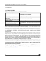
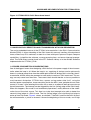
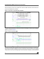
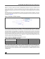
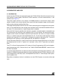
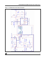
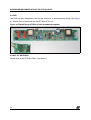
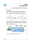
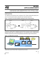
AN1900
APPLICATION NOTE
HARDWARE IMPLEMENTATION FOR ST7DALI-EVAL
INTRODUCTION
This application note describes how to implement a DALI (Digital Addressable Lighting Interface) in an existing high-frequency dimmable tube-lamp ballast application.
Figure 1. Hardware overview with MCU handling only DALI communication
If necessary, please refer to Application Note AN1756 “Choosing a DALI implementation
Strategy with ST7DALI” for further background. This application note is issued with the
ST7DALI evaluation board which can be purchased with the sales type ST7DALI-EVAL.
Figure 2. ST7DALI-EVAL principle
Ballast
DALI
Master
1-10 V
DALI
Master
Board
Ballast
DALI Slave
Software
1-10 V
DALI
Slave
Board
DALI
Slave
Board
Up to 64 slaves
DALI Evaluation Kit
Please refer to the ST7DALI-EVAL Evaluation Kit user manual.
Rev. 1.0
AN1900/0504
1/9
1
HARDWARE IMPLEMENTATION FOR ST7DALI-EVAL
1 HARDWARE
1.1 ST7DALI FEATURES
Table 1. List of Requirements for the Microcontroller
Minimum Requirements
26 bytes of EEPROM, to save non-volatile parameters
3 Kbytes program memory
A timer with Input Capture/Output Compare capabilities to receive and transmit
DALI signals.
Low-consumption mode, to save energy
between commands.
ST7DALI Features
256 bytes data internal EEPROM
8 Kbytes Flash program memory
DALI communication module (DCM).
Halt power saving mode
Up to 15 multi-functional I/Os, one 12-bit Auto-reload Timer
I/Os and PWM outputs to perform the inwith 4 PWM outputs, input capture and output compare functerface with the ballast controller.
tions
A clock source
Internal 1% RC oscillator,
In addition to DALI protocol handling, but without fully controlling the ballast, the microcontroller can also monitor or customize some ballast parameters, e.g. for easy calibration of various power levels in the factory, and/or act as a supervisor of the complete ballast parameters.
1.2 INTERFACE BETWEEN MICROCONTROLLER AND ANALOG HALF-BRIDGE
CONTROLLER
A potential hardware problem is the interface between the microcontroller and the analog halfbridge controller. One possibility is to use PWM outputs and to filter them to create analog setpoints for the half-bridge controller. The 4 PWM outputs of the Autoreload timer enable
ST7DALI to act on up to 4 different “external parameter” pins of the half-bridge controller, for
example L6574, without computation load (Please refer to AN993: L6574 & Microcontroller in
ballast applications). The designer is then in total control of the lamp.
Another easier solution is to keep the 1-10V input widely used for dimming level control, and
use the microcontroller as a “gateway” or interface between the DALI bus and the analog input
of a conventional analog dimmable ballast. The microcontroller is then no longer in direct connection with the analog ballast controller.
Based on this topology, a DALI demonstration board based on the ST72F334J4 has been
built. For this purpose, a dedicated ST7DALI has been developed and its associated evaluation board can be seen in Figure 3.
2/9
2
HARDWARE IMPLEMENTATION FOR ST7DALI-EVAL
Figure 3. ST7DALI-EVAL DALI Slave demo-board.
1.3 HANDLING DALI RECEPTION AND TRANSMISSION WITH DCM PERIPHERAL
The major embedded feature of the ST7DALI microcontroller is the DALI Communication
Module (DCM). It allows decoding of the DALI forward frame and sending of the backward
frame, without any CPU overhead, or need for a timer with Input Capture or Output Compare
capabilities. It simplifies the software, saves processing time, and eases interrupt management. The DCM drivers can be found in the ST7 Software Library or in the AN1601 Software
Implementation for ST7DALI_EVAL.
1.4 POWER CONSUMPTION CONSIDERATIONS
One of the biggest issues when designing a DALI ballast is the power supply of the microcontroller when the lamp is off. When the lamp is on, supplying all devices can be quite easily
done via a charge pump taken from the middle point of the half-bridge. But in stand-by, the microcontroller should always be powered-on and ready to receive a DALI command. This energy can only come from the mains. The current taken should then be as low as possible to
avoid constant dissipation. ST7DALI has a power saving mode called “halt”, using the
smallest power consumption, since everything inside the MCU (core, peripherals and clock
source) is “frozen”. After entering this mode, only a reset or an external interrupt can wake up
the microcontroller. The interrupt can be triggered by the first (falling) edge of the DALI frame.
When this happens, Run mode is not immediately operational, mainly because of the stabilization time of the clock source. This time has to be short enough to be able to detect the
second (rising) edge of a DALI frame. The first (falling) edge is not significant but helps to
wake up from Halt mode. Figure 4. shows, on channel 1, the DALI frame on the DALI IN pin of
the microcontroller, a pulse on channel 3 shows the beginning of the run mode, and a high
3/9
HARDWARE IMPLEMENTATION FOR ST7DALI-EVAL
level on channel 4 shows that a proper DALI frame has been received, and that the data is
ready to be handled by the software.
Figure 4. Overview of a forward frame reception
To better understand how the ST7DALI can wake up fast enough, a zoom on the first edge is
needed, as shown in Figure 5.
Figure 5. Zoom on the first edges
When the first falling edge is detected, the microcontroller leaves Halt mode for a transition period of 256 clock cycles. At 8MHz, this means around 32µs. Since the DCM starts sampling
125µs (worst case) after the falling edge, the microcontroller frequency can be reduced to
4/9
HARDWARE IMPLEMENTATION FOR ST7DALI-EVAL
4MHz (i.e. 64µs to wake up from halt). Although the software can work at 1MHz and still
comply fully with DALI, it is then not possible to use Halt mode for additional power saving at
this frequency because the wake up is not fast enough to catch the beginning of the incoming
frame.
When the lamp is off, the microcontroller is not the only source of power dissipation. The hardware interface between the DALI bus and the microcontroller also takes quite some current,
as shown in Figure 6.
Figure 6. DALI Bus- ST7DALI interface
When the bus is high (steady state), 500µA is always flowing through the resistor. Because
the microcontroller should always know if the bus is constantly low (bus failure), an alternative
and more power-saving topology is not possible. On the one hand, current in the resistor
should be as low as possible, but on the other hand it should not be so low that any noise fools
the microcontroller. When the transistor turns off, the current should be high enough to evacuate the carriers within the right time frame. 10KOhms is a good trade-off (please refer to the
I/O ports section of the ST7DALI data sheet).
Here is a summary, depending on the frequency chosen:
Table 2. Power Consumption Overview
Interface
ST7DALI
Total @5V
Halt Mode
(fCPU run=4MHz)
500µA
10µA
170mW
Run Mode
(fCPU run=1MHz)
500µA
2,7mA
890mW
Finally, the accuracy of the ST7DALI ADC is directly proportional to the VDD regulation accuracy. If the microcontroller supply is regulated with a standard zener diode for example, the
ADC precision would be around 10%. If precise measurements have to be performed, then a
voltage regulator with low quiescent current and high precision is needed, typically from the
LD2980 series.
5/9
HARDWARE IMPLEMENTATION FOR ST7DALI-EVAL
2 SCHEMATICS AND PCB
2.1 SCHEMATICS
Aside from the ST7DALI microcontroller itself, the ST7DALI-EVAL DALI Slave board has four
main sections: Power Supply, DALI Bus-ST7DALI Interface, In-Circuit Communication, 1-10V
Interface (see Figure 7.).
The power supply section is very simple. A LD2980 provides an accurate 5V output, while
jumper 4 allows you to easily measure the current used by the power supply, the microcontroller and the interface with the DALI Bus.
The bridge diode protects the DALI Bus-ST7DALI interface against wrong polarity wiring however it is not protected from over-voltage from accidental mains connection between the control wires. For such protection, a high voltage switch is needed.
Since the DALI Protocol specifies that isolation is required, two optocouplers are needed: one
for transmission (U4) and one for the reception (U5). For cost reasons, the transmission optocoupler cannot sustain the 250mA required to pull the DALI bus down (it is high in steady
state), so a power stage has to be implemented via Q1. For the bus to be kept down during
transmission, capacitor C7 is used since a voltage must remain on the base of Q1. To avoid a
discharge of this capacitor via the optocoupler U5, the diode D6 is required.
Finally the zener diode D5 is used to ensure that the wide voltage specifications of the DALI
bus (High level: 9.5 to 22.5 V. Typical 16 V. Low level: -6.5 to +6.5 V. Typical 0 V) can be fulfilled.
The ST7 In-Circuit Communication (ICC) allows In-Circuit Programming (ICP) and In-Application Programming (IAP). Please refer to the FLASH PROGRAM MEMORY section of the
ST7DALI datasheet.
A standard dimmable ballast can be easily driven through the evaluation board with the 1-10V
Interface. A PWM with programmable duty cycle is generated by the ST7DALI, filtered to a DC
value proportional to the duty cycle, and amplified from 0-5V to 1-10V through to the operational amplifier U2A.
Regardless of whether a ballast is available or not, the LED LD3 gives an overview of the light
level.
6/9
HARDWARE IMPLEMENTATION FOR ST7DALI-EVAL
Figure 7. ST7DALI-EVAL DALI Slave Schematic
7/9
HARDWARE IMPLEMENTATION FOR ST7DALI-EVAL
2.2 PCB
The PCB has been designed to look like the add-on to an existing ballast design (see Figure
8.). Gerber files are delivered with the ST7DALI-EVAL kit.
Figure 8. EVAL6574 and ST7DALI-EVAL demoboards together
2.3 BILL OF MATERIAL
Please refer to the ST7DALI-EVAL User Manual.
8/9
HARDWARE IMPLEMENTATION FOR ST7DALI-EVAL
“THE PRESENT NOTE WHICH IS FOR GUIDANCE ONLY AIMS AT PROVIDING CUSTOMERS WITH INFORMATION
REGARDING THEIR PRODUCTS IN ORDER FOR THEM TO SAVE TIME. AS A RESULT, STMICROELECTRONICS
SHALL NOT BE HELD LIABLE FOR ANY DIRECT, INDIRECT OR CONSEQUENTIAL DAMAGES WITH RESPECT TO
ANY CLAIMS ARISING FROM THE CONTENT OF SUCH A NOTE AND/OR THE USE MADE BY CUSTOMERS OF
THE INFORMATION CONTAINED HEREIN IN CONNECTION WITH THEIR PRODUCTS.”
Information furnished is believed to be accurate and reliable. However, STMicroelectronics assumes no responsibility for the consequences
of use of such information nor for any infringement of patents or other rights of third parties which may result from its use. No license is granted
by implication or otherwise under any patent or patent rights of STMicroelectronics. Specifications mentioned in this publication are subject
to change without notice. This publication supersedes and replaces all information previously supplied. STMicroelectronics products are not
authorized for use as critical components in life support devices or systems without express written approval of STMicroelectronics.
The ST logo is a registered trademark of STMicroelectronics.
All other names are the property of their respective owners
© 2004 STMicroelectronics - All rights reserved
STMicroelectronics GROUP OF COMPANIES
Australia – Belgium - Brazil - Canada - China – Czech Republic - Finland - France - Germany - Hong Kong - India - Israel - Italy - Japan Malaysia - Malta - Morocco - Singapore - Spain - Sweden - Switzerland - United Kingdom - United States
www.st.com
9/9