1
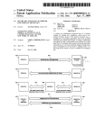
US007652723B1
(12) United States Patent
(10) Patent N0.2
Patton et al.
(54)
(75)
(45) Date of Patent:
Jan. 26, 2010
COMPOSITE VIDEO SIGNAL CORRECTION
4,851,842 A
7/1989 lwamatsu
UNIT FOR VIDEO IMAGING AND VIDEO
RECORDING SYSTEMS
4,853,792 A
4,982,191 A
8/1989 Katsuta et a1.
1/1991 Ohta
Inventors: David Patton, Louisville, CO (US);
Richard Frey, Louisville, CO (US);
Edward Brannan, Erie, CO (US)
5,012,330 A
4/1991 Bugni
5,057,932 A
5,086,437 A
5,164,839 A
10/1991 Lang
2/ 1992 Tomita
11/1992 Lang
5,218,449 A
(73) Assignee: Video Accessory Corporation, Boulder,
Notice:
6/1993 K0 et a1.
5,276,517 A
1/1994 Matsuzawa et 31,
Subject to any disclaimer, the term ofthis
patent is extended or adjusted under 35
5,280,356
5,341,173
5,422,804
5,627,898
1/1994
8/1994
6/1995
5/1997
U-S-C- 154(1)) by 806 days-
5,644,263 A
CO (Us)
(*)
US 7,652,723 B1
A
A
A
A
Hiramatsu
Hyeon
Clark
Washino
7/1997 Clark
(21) Appl.No.: 11/082,370
(22) Filed:
Mar. 16, 2005
(Continued)
Related US. Application Data
(60)
OTHER PUBLICATIONS
Provisional application No' 60/563’751’ ?led on Apr'
“Solutions for Genlocking,” VACSync Times, Issue 1 (1995),6pages.
19, 2004, provisional application No. 60/662,914,
(Continued)
?led on Mar. 15, 2005.
Primary ExamineriTrang U Tran
(74) Attorney, Agent, or FirmiSheridan Ross P.C.
(51)
Int. Cl.
H04N 5/16
(52)
us. Cl. ..................... .. 348/691; 348/692; 348/695;
(2006.01)
(57)
ABSTRACT
348/525
(58)
Field of Classi?cation Search ............... ..
348/691,
I
348/692i698, 525, 521, 526527’ 689, 673,
348/677’ 572
See application ?le for Complete Search history
(56)
U.S. PATENT DOCUMENTS
2
.
1
.
t
.
.d d
(b) DC restore circuitry 416 operable to set an average DC
voltage of a ?rst portion of the DC-adjusted analog video
signal to a ground reference voltage to yield a DC
7/1930 Baggett et 31
10/1981 Geum
1(7);
t
(a) av1deo 1nput 400 operable to rece1ve a ?rst analog v1deo
s1gnal and remove the DC voltage offset component
from the video signal to form a DC-adjusted analog
video signal; and
References Cited
4,215,371 A
4,296,437 A
b d.
11 one em 0 1men , a s1gna process1ng sys em 1s prov1 e
that mcludes:
.
.
153M101? et 31'
adjusted analog video signal. The DC-restored analog
4’575’755 A
4651213 A
3/1986 sfhogggberger et 31
3/1987 Takimoto
video signal is then provided to anAnalog-to-Digital or
A/D Tonverter 112 for convers1on 1nto a d1g1tal v1deo
slgna '
4,680,633 A
7/1987 Gerdes et a1.
4,719,584 A
1/1988 Rue et :11.
4,849,906 A
7/ 1989 Chodos et a1.
400
Signal
13 Claims, 8 Drawing Sheets
404
AC
Input-7| Coupling
D'ff
4033
ti [
I ire/Ell a
4(2
Gain
/416
50
DC
Control H Control
P
ReJore l‘uw “"1 Tim? I
Signal Output
/
516
Video Signal
Synch
"
J
Comparison
Legend:
1
__> Video Signal Path
_
---> Control Signal Path
Signal Path Junction
—\
520
I
Vlde° s'gnal
‘
lll?liimgzl
comibarison \524
To Monitoring
1
Timing
Veri?cation
Microprocessor
-\
528
....... ,1
US 7,652,723 B1
Page 2
US. PATENT DOCUMENTS
5,659,313
5,689,308
5,798,802
5,818,672
5,867,222
5,892,555
5,952,945
5,986,719
5,990,741
5,995,157
5,995,166
5,995,705
6,016,113
6,107,887
6,127,956
6,147,633
6,160,443
6,204,784
6,268,814
6,288,658
6,307,492
6,317,473
6,320,627
6,320,917
6,326,911
6,356,221
6,377,196
6,417,794
6,433,723
6,459,447
6,459,458
6,492,924
6,509,796
6,515,542
6,515,600
6,525,609
6,529,248
6,556,158
6,559,788
6,580,465
6,584,365
6,611,537
6,618,480
6,628,730
>
8/1997
11/1997
8/1998
10/1998
2/1999
4/1999
9/1999
11/1999
11/1999
11/1999
11/1999
11/1999
1/2000
8/2000
10/2000
11/2000
12/2000
3/2001
7/2001
9/2001
10/2001
11/2001
11/2001
11/2001
12/2001
3/2002
4/2002
7/2002
8/2002
10/2002
10/2002
12/2002
1/2003
2/2003
2/2003
2/2003
3/2003
4/2003
5/2003
6/2003
6/2003
8/2003
9/2003
9/2003
Dischert et al.
Nayebi
Elmis et al.
Hilbe
Norris et al.
Sohn
Latham et al.
Nakamura
Yamamoto et al.
Retter et al.
Kawano
Lang
Binder
Zucker et al.
Agi
Ukawa et al.
Maalej et al.
Hat?eld
Kolsrud
6,640,093 B1
6,653,959 B1
10/2003 Wildhagen
11/2003 Song
6,664,907
6,665,308
6,680,680
6,683,554
6,684,065
6,690,311
6,703,958
12/2003
12/2003
1/2004
1/2004
1/2004
2/2004
3/2004
B1
B1
B1
B2
B2
B2
B2
Knepper et al.
Rakib et al.
Mellot
Nikai et al.
Bult et al.
Lundin et al.
Noro
6,704,673 B2
3/2004 McTigue
6,734,817
6,738,002
6,744,320
6,744,832
6,759,904
6,788,230
6,795,496
B2
B2
B2
B2
B2
B2
B1
5/2004
5/2004
6/2004
6/2004
7/2004
9/2004
9/2004
6,798,286
6,798,293
6,803,829
6,816,096
B2
B2
B2
B2
9/2004
9/2004
10/2004
11/2004
Naka et al.
Ercan et al.
Nguyen et al.
Miao
Behzad
Ahn
Soma et al.
Dauphinee et al.
Casper et al.
Duncan et al.
Comer et al.
Mestdagh et al.
Berranger et al.
6,816,204 B2
11/2004 Limberg
6,822,601 B1
11/2004 Liu et al.
Stott et al.
Scott et al.
Stott et al.
Gomez et al.
6,831,576 B2
6,833,875 B1
12/2004 Geiger et al.
12/2004 Yang et al.
LeChevalier
Kolsrud et al.
Munoz et al.
Randall
Okada et al.
Balaban
OTHER PUBLICATIONS
“Solutions for Ground Loop Interferences,” VAC Sync Times, Issue 1
(1994), 4 pages.
Kramer Electronics, Ltd., “User Manual Model 104LN” (undated),
pp. 1-5.
Kramer Electronics, Ltd., “User Manual Distribution Ampli?ers
Copley et al.
Models VM-1010, VM1015, VM-1021, VM-1042, VM-1044,
Nguyen et al.
Wang et al.
VN-1055, VM-54” (undated), pp. 1-22.
Tsyrganovich ............ .. 348/691
“The Electric BulletiNeWest Technology Topping the Security
Dealer Chart,” WWW.secdealer.com (Mar. 2003), p. 20.
Micronas Preliminary Data Sheet, “VPC 3205C, VPC 3215C, Video
Processor Family,” (Oct. 19, 1998), 6251-457-2PD, pp. 1-48.
Steensgaard-Madsen
Murphy
ConeXant Production Data Sheet, “CX25836/7 Video Decoder,”
102267A (Sep. 2004), pp. 1-1-6-6.
Graen
Behzad
Sato
......................... .. 348/689
Blanchard
Edens et al.
VAC ProSeries Products, “1X4 Equalizing Distribution Ampli?er,
FleXPWr, for Belden 8281 Cable,” Video Accessory Corporation
(undated), 2 pages.
Polley et al.
Stott et al.
* cited by examiner
US. Patent
Jan. 26, 2010
Sheet 1 of8
US 7,652,723 B1
100
104
112
ND Converter /
Digital Display
Enhancement
And/Or Recording
Device(s)
Fig. 1
(Prior Art)
US. Patent
Jan. 26, 2010
Sheet 3 0f 8
US 7,652,723 B1
100
104
300
Signal
Correction
-/
Unit
/
304
ND Converter
Digital Display
Enhancement
And/Or Recording
Device(s)
Fig. 3
/'108
US. Patent
Jan. 26, 2010
Sheet 4 of8
US 7,652,723 B1
Analog Composite Video Signal IN
.i r
B
mm“H U.
m
n
or H
mm.
H
%
C
ct
m
.ww
@
..m.
N
4
cI-
mm
H4
0
mm
n
m
4%
mm
w
W
n
5.m
D.AluCmA
mm
v".M:
m
VMy“Vo UeSlIf
w
M
be
mCl
m.
.mw.
4ma
Fm.
mSP
m
G.mvZ
4Have
08au4
HT
M“
.n
tE
ie
n"
M
.4
m4
w
m
W
we
4
/
0<
mD
M
0mO
dl
w
m
.w.A
m
<
w
1.alm
e 2m
m
.m
0
Sd5
a;
te
.m
4t
DC Restore
2'.
Amm}ifrwm nM\" 6‘Ik'mfw
_
k
m
.mD
"
5.mDm
2in .Hwh tr
d
4A
46
m
4C O
.
C
md
6e
a .w r
@
M.
M
4 01.Alu
iOMU T8
5
m
m
d .m
Signal
Bypass for PZT
Corrected video OUT
Legend:
Fig. 4
—> Video Signal Path (arrow indicated ?ow)
----> Alternative Video Path (arrow indicates ?ow)
> Control Signal Path (arrow lndlcates ?ow)
US. Patent
Jan. 26, 2010
Sheet 5 of8
US 7,652,723 B1
B
N
I- 05E;
wcozm t>
.w9V./8l:.
n/.|-cowvmmcmnEo
\
<um 59:0
555. u‘7Q“W 6&5
82>
5oi:t.uvz91nEq$“m mcow/mQ\mEo
\
8“,2%
Mn$2.52“
63805.2
>obmEBEoE
Mow
NP
\
©:~\
\
p.m >
Qm nucm j
‘o<lwE0oGm?ocQEgiA1w
E8M_£625m3A>:c.30-_wIx3l.o5‘cEmzCcQas?W
il5\'965:096:8m0
>55%8£32A>l.
m.mt
US. Patent
Jan. 26, 2010
Sheet 7 of8
R11
3300
(
US 7,652,723 B1
800
c
1|.1F
V
1 CTRL CMEXT
This
_REF
-———EVCTRL vs+ 5
R6
3 VINP
R5
R7 R9
'v\.
‘TVINM
L_
F“
[3
vs -
ENBL 4
VOUT
E CMOUT VSA
R12
C1
3309 1 HF;
7 VGAIN
55
LOGIC
_REF
Cal C9__
Fig. 7
WW
VSA+1
OV
X2
l C11
US. Patent
Jan. 26, 2010
Sheet 8 of8
US 7,652,723 B1
@@E
H302
US 7,652,723 B1
1
2
COMPOSITE VIDEO SIGNAL CORRECTION
UNIT FOR VIDEO IMAGING AND VIDEO
RECORDING SYSTEMS
signal levels. When the analog composite video signal fed to
the A/ D converter is degraded, the resulting digital video
signal may be distorted. For example, the sync tip 204 may be
dis?gured. This distortion may be very slight or severe,
depending on the type and level of degradation to the analog
CROSS REFERENCE TO RELATED
APPLICATION
video signal.
The most common causes of composite video signal dis
tortion in video imaging and video recording systems are as
folloWs:
Signal loss in the transmission means. This loss may be due
The present application claims the bene?ts of US. Provi
sional Application Serial Nos. 60/563,751, ?led Apr. 19,
2004, and 60/662,914 ?led Mar. 15, 2005, of the same title
and to Patton, et al., each of Which is incorporated herein by
this reference.
to attenuation, mismatched transmission lines, splitters
or other passive devices Within the transmission path.
LoW output from the video source. If the signal output from
FIELD OF THE INVENTION
the video camera or other source is not of su?icient ampli
The present invention relates generally to video imaging
and video recording systems and speci?cally to video imag
meet the desired standard even if the transmission line is
tude, the video signal at the input to the A/ D converter may not
virtually lossless.
Interference due to ground loops. Ground loops result
ing and video recording systems including one or more ana
log composite video cameras or other video sources, and
digital display, enhancement, or recording equipment that
20
incorporates analog to digital conversion means.
When the ground potential is different betWeen tWo compo
nents Within a video system. This difference in ground poten
tial can result in “hum bars” on the video picture caused by 60
HZ commercial poWer, or herringbone interference on the
BACKGROUND OF THE INVENTION
video picture caused by AM broadcast signals, or a combina
tion of 60 HZ and AM broadcast interference that can result in
Video imaging systems are used in a broad variety of
applications, including telecommunications, entertainment,
hum bars, herringbone, blanking, color distortion, or other
degradation to the video picture.
security monitoring, and the like. Video imaging systems are
generally placed in one of tWo categories, namely computer
and television. In television applications, baseband video sig
DC Offset. A DC voltage may be superimposed on the
video signal by the video source or by another device
nals can folloW a number of different formats, including the
National Television Systems Committee or NTSC standard
25
Within the signal path. If suf?ciently large, the DC offset
30
can result in physical damage to the A/D conversion
means and/or to other components Within the system.
Even a small DC offset may not cause noticeable deg
radation to the video picture in an analog system but may
35
above. Many video components utiliZe AC coupling to
eliminate DC offset, hoWever, this approach results in
the signal not having a ?xed (e. g., DC) reference, Which
is critical to producing an analog composite video signal
40
One exemplary application for the present invention is
(the US. and Japan standard), the Phase Alternating Line or
PAL standard (the European standard), and the High De?ni
tion/ Standard De?nition Digital Television format.
In television, there are three basic levels of baseband signal
interfaces. In order of increasing quality, they are composite
cause errors in the A/ D conversion process as described
video (or Color, Video, Blanking, and Sync or CVBS), Which
uses one Wire pair, Y/C (or S-video), Which uses tWo Wire
pairs, and component, Which uses three Wire pairs. Each Wire
pair includes a signal and a ground. Composite signals are the
most commonly used analog video interface and combine the
brightness information (luma) and the color information
(chroma) and the synchronizing signals on just one cable.
FIG. 2 depicts the horizontal blanking portion of a typical
NTSC composite video Waveform that includes color infor
that fully meets the NTSC or PAL speci?cations.
video security systems, such as that shoWn in FIG. 1. Such
systems typically incorporate a multiplicity of video cameras
100 in continuous operation. The analog composite video
signals from these cameras are transmitted via a transmission
45
mation and represents one horiZontal scan line. The signal
includes a front porch 200 (Which is the area of the signal
betWeen the end of the active video and the leading edge of a
sync pulse), the sync pulse or tip 204, (Which provides syn
chroniZing timing information), a breeZeWay 208 (Which is
the area of the signal representing the time betWeen the rising
edge of the synch pulse 204 and the start of a color burst 212,
the color burst 212 (or color subcarrier) (Which is 8-10 cycles
of the color reference frequency and is positioned betWeen the
rising edge of the sync pulse and the start of the active video),
and the back porch 216 (Which is the time betWeen the end of
the color burst and the start of active video).
location most commonly accept baseband composite video
50
recorders. NeW systems and upgrades to existing video secu
rity systems typically incorporate one or more digital video
recorders, or DVRs, that are designed to accept analog base
55
band video signals. A/D conversion circuitry 112, Which is
typically integrated Within the DVR, is designed to Work With
either or both of the tWo signal standards (NTSC and PAL).
When the input video signal is even slightly degraded and
60
cess may distort the digitiZed video signal, causing the result
ant video picture to be signi?cantly Worse in terms of picture
In video imaging and video recording systems, analog
does not meet the desired standard, the A/D conversion pro
ing. While it is desirable that the analog composite video
signal input to an analog-to-digital (A/D) converter fully
meets the appropriate composite video standard (either the
NTSC or PAL standards), in practice the composite video
signal is often degraded and does not meet the desired stan
dard due to some combination of loW signal output from the
video camera, signal loss, interference, or improperAC or DC
signals folloWing either the NTSC format or the PAL format.
Until recently, most video security systems utiliZed analog
composite video signals are often converted to a digital video
signal for subsequent enhancement, display, and/or record
line 104 (e.g., coaxial cable, tWisted pair, ?ber optics, or radio
being the most common transmission line) to a central loca
tion Where the video signals may be monitored and are
recorded. The video monitors and recorders 108 at the central
quality than Would be the case With an analog video recorder.
Whereas an analog video recorder might record a useable,
though degraded, picture, the picture recorded by the DVR
65
may be distorted to such an extent that much or all of the
information is lost. Additionally many DVRs are designed to
detect motion Within the video picture based on an algorithm
US 7,652,723 B1
4
3
performed on the digitized video signal. If the digitized video
(c) setting an average voltage of a ?rst portion of the
signal is not an accurate and true representation of the video
adjusted analog video signal (the ?rst portion can, for
picture captured by the video camera, then the DVR algo
example, be one or more of the front porch, breezeWay, color
rithm may falsely detect motion When no motion is present, or
burst, and back porch) to a ground reference voltage to pro
duce a restored video signal.
In one con?guration, the restored video signal is converted
into a digital video signal Without the problems caused by
unWanted DC offsets and loss of the DC reference voltage
from the video signal. After removal of the DC offsets and
conversely not detect motion When motion is actually present.
In the ?rst instance, the DVR Will rapidly ?ll its available
digital storage medium resulting in loss of data due to either
insuf?cient storage capacity or earlier data being overwritten;
in the second instance, the DVR Will not record the desired
data at all.
The common causes of video signal degradation Within a
before DC reference voltage restoration, the DC-adjusted
analog video signal may further be passed through a differ
ential input to remove ground loop interference.
video security system are Well understood by video engineers
and other experienced technical people. HoWever, video
security system installers typically have neither the necessary
training to knoW the causes of video signal degradation, the
To compensate for signal losses in the transmission line
from the video source and loW poWer output from the video
needed test equipment (or training) to identify the speci?c
source, the analog video signal, after being passed through
the differential input may be further processed by adjustable
cause of degradation in a video system installation, nor the
knowledge to determine the most cost-effective solution even
if the cause of a problem is identi?ed. Additionally, in many
installations the level of video signal degradation Would be
gain and equalizer circuitry. The adjustable gain circuitry
20
ampli?es all components of the video signal equally While the
acceptable With an analog video recorder but results in severe
equalizer circuitry ampli?es only higher frequency compo
picture degradation, continuous recording, or no recording,
nents.
When a DVR is installed. There is currently no system able to
simultaneously correct many of the common causes of video
Applications for this embodiment of the present invention
include, but are not limited to, security systems, video imag
signal degradation Within a video security system. With the
increasing use of digital video recorders in video security
25
Until the present invention, there has been no single device
systems, the need for such a solution is immediate and groW
that speci?cally corrects for the common causes of composite
ing.
Another application for the present invention is video
imaging systems. Analog composite video cameras are com
30
monly used to capture video pictures that are converted to a
digital video signal, then digitally manipulated or enhanced,
displayed and/ or recorded. Such applications, Which include
medical, satellite and airborne imaging systems, utilize an
A/D conversion process as described above, and these sys
tems may suffer from the same distortion effects described
ing, and radar display systems.
35
above if the analog video signal input is degraded. Since
video signal degradation to ensure that the corrected analog
video signal nearly meets, or most preferably fully meets, the
desired composite video standard prior to anAnalog-to-Digi
tal or A/D conversion process Where the resulting digital
video signal is enhanced or otherWise digitally manipulated,
displayed, and or recorded. The digital replica of the analog
video signal can be relatively free of distortion, causing the
resultant video picture to be of high quality and providing a
high degree of accuracy in motion detection (as more accurate
imaging systems typically require the highest possible picture
detection of pixel changes betWeen frames). The analog-to
resolution, any loss of intelligence due to degradation of the
digital orA/ D converter, due to the high standard of the analog
analog composite video system is highly undesirable.
40
Another application for the present invention is radar sys
tem displays. In many radar systems, the output from the
radar receiver is a composite video signal. Many radar sys
ciated, signi?cant reductions in video ?le size equate to loWer
tems digitally enhance the displayed signal. Such systems
utilize an A/D conversion process as described above, and
these systems may suffer from the same distortion effects
memory requirements, thereby avoiding the need for costly
45
described above if the analog video signal input is degraded.
Such display systems are utilized to produce the highest pos
sible picture resolution, and the loss of intelligence due to
degradation of the analog composite video system is highly
50
undesirable.
55
embodiments and con?gurations of the present invention.
These and other advantages Will be apparent from the
disclosure of the invention(s) contained herein.
are open-ended expressions that are both conjunctive and
60
In one embodiment of the present invention, a signal pro
disjunctive in operation. For example, each of the expressions
“at least one ofA, B and C”, “at least one ofA, B, or C”, “one
or more of A, B, and C”, “one or more of A, B, or C” and “A,
B, and/ or C” means A alone, B alone, C alone, A and B
together, A and C together, B and C together, and A, B and C
reference;
component) from the video signal to form an adjusted analog
video signal; and
conversion process. By providing a compliant video signal to
the A/D converter, the resolution Will not be adversely
“one or more of. . . an ”, “one or more of. . . or”, and “and/or”
cessing method is provided that includes the steps of:
(a) receiving a ?rst analog video signal that includes a ?xed
(b) removing the ?xed reference (e.g., DC voltage offset
While the absolute resolution of the system is constrained by
the camera resolution and the recording parameters of the
Digital Video Recorder or DVR (Which are typically user
de?ned), the resolution can also be impacted by the A/D
As used herein, “at least one . . . and”, “at least one . . . or”,
The present invention is generally directed to a signal correc
tion unit that removes noise and/or corrects various signal
errors prior to conversion of the analog video signal into a
digital video signal.
hard drives or limiting the time that the data can be stored.
impacted by the digitization of the video signal.
SUMMARY OF THE INVENTION
These and other needs are addressed by the various
video signal, can create feWer artifacts (noise) and the com
pression scheme can Work more e?iciently. As a result, the
video ?le size can be reduced signi?cantly. As Will be appre
65
together.
The above-described embodiments and con?gurations are
neither complete nor exhaustive. As Will be appreciated, other
US 7,652,723 B1
5
6
embodiments of the invention are possible utilizing, alone or
412, and Direct Current or DC restore circuitry 416. The A/C
in combination, one or more of the features set forth above or
input coupling accepts large DC voltage offsets on the input
analog composite video signal to accommodate most instal
described in detail beloW.
lations4even unusual combinations of hardWare that result
BRIEF DESCRIPTION OF THE DRAWINGS
in an unacceptably high magnitude DC voltage component.
The differential input circuitry 404 automatically eliminates
or minimizes ground loop interference. The (automatically
and/or manually) adjustable gain and EQ circuitry 408 and
FIG. 1 is a block diagram of a video imaging system
according to the prior art;
FIG. 2 depicts a video signal in accordance With the
National Television Systems Committee or NTSC format;
FIG. 3 is a block diagram of a video imaging system
according to an embodiment of the present invention;
FIG. 4 is a block diagram of a video signal correction unit
according to an embodiment the present invention;
FIG. 5 is a block diagram of a video signal correction unit
according to an embodiment of the present invention;
FIG. 6 is a circuit diagram of the DC restore circuitry
according to an embodiment of the present invention;
FIG. 7 is a partial circuit diagram of the differential input
and adjustable gain and equalizer according to an embodi
ment of the present invention; and
FIG. 8 is a partial circuit diagram of the adjustable gain and
equalizer according to an embodiment of the present inven
412 alloWs for signal optimization, even With signi?cant
transmission line loss and/or loW signal levels from the video
source. The DC restore circuitry 416 automatically provides
the correct DC voltage levels on the composite video signal.
By positioning the above subcomponents on each of the video
channels, the unit 300 can simultaneously process one or
more analog composite video signals being conducted or
having components being conducted on multiple channels.
As Will be appreciated, A/C coupling 400 is implemented
by locating capacitive couplers on each video input/channel.
20
Stated another Way, in each incoming coax transmission line
a capacitive coupler is connected in line With each of the
center conductor and shield. Because the capacitors Will not
pass DC voltage components, such as DC offsets, capacitive
coupling Will remove from the composite analog signal any
tion.
25
DC offset (or ?xed reference) on the transmission line 104. In
a preferred con?guration, A/C coupling removes all of the DC
DETAILED DESCRIPTION
offset in the input composite analog video signal. Any suit
able A/C coupling capacitors may be employed.
As depicted in FIG. 3, the video signal correction unit 300
of the present invention is positioned upstream of the A/D
converter 112 and digital display enhancement and/ or record
The differential input 404 results in a high impedance path
betWeen the unit’s input and output signal ground references.
30
ing device(s) 108 (and in the signal pathbetWeen the device(s)
108 and the A/D converter 112) to correct for the common
causes of composite video signal degradation before the com
420 betWeen the center conductor and shield of the coax
posite video signal is input into the digital display enhance
ment and/ or recording device(s). Preferably, the unit 300 is
35
separate from or integral With the A/ D converter. When con
?gured as a separate component, the unit 300 is preferably
positioned in close proximity to or adjacent to the converter
112, With a transmission line 304 connecting the signal cor
rection unit 300 to the camera 100 (or composite video
source). The distance betWeen the composite video source
and the signal correction unit 300 may vary betWeen a feW
feet to over 1,000 feet, as determined by the user’s require
ments. Typically, the signal correction unit 300 and the A/D
This high impedance path greatly reduces, and most prefer
ably eliminates, undesirable ground loop currents. Speci?
cally, the differential input references the input video signal
cable. The input connector is not grounded, and the input
signal is not referenced to the ground. By isolating the input
signal shield from the output signal ground, the ground seg
ment of the signal path is broken. The signal input and output
impedances are independent of the impedance betWeen the
input shield and the output signal ground and are selected to
40
match the impedance of the transmission lines (typically coax
cable) 104 and 304 respectively. Preferably, the differential
input impedance ranges from about 50 to about 909, With an
impedance of about 759 being most preferred.
The adjustable gain circuitry 408 alloWs for adjustment of
converter 112 are electronically adjacent to one another and
even more preferably are mounted in the same equipment
the video signal amplitude (or IRE levels). The adjustable
gain circuitry 408 can be any ampli?er that ampli?es equally
rack. More preferably, the cumulative signal loss in the com
all of the video signal frequency components by a desired
posite video signal along transmission line 304 before being
gain. This is intended to restore the sync tips 204 to the proper
input into the A/D converter and digital display enhancement
and/ or recording device(s) 108 is no more than about 0.25 dB
magnitude (or IRE level). Preferably, the signal poWer is
50
and even more preferably no more than about 0.1 dB. The
signal transmission line may be any conductor, With coaxial
or tWisted pair being preferred.
Although the preferred embodiment is discussed With ref
erence to NTSC-type analog composite video signals, it is to
be understood that the embodiment can operate equally With
55
HDTV component video signals, Red Green Blue or RGB
component video signals, Video Graphics Array orVGA-type
faces.
The subcomponents of the signal correction unit 300 are
depicted in FIG. 4. The unit 300 includes Alternating Current
or A/ C coupling 400, differential input circuitry 404, adjust
able gain circuitry 408, adjustable Equalizer or EQ circuitry
4 db).
The adjustable EQ circuitry 412 alloWs for frequency
dependant adjustment of the video signal amplitude and is
used to compensate for the high-frequency roll-off that is
inherent in many types of transmission lines, particularly, but
not limited, to coaxial cable and tWisted pair. The adjustable
other types of video signals, such as PAL-type video signals,
video signals, and Extended Graphics Array or XGA-type
signals over any suitable video interface, including not only
composite signals but also Y/C and component video inter
adjusted by an amount ranging from about 0.5>< to about 4x
(or from about —3 db to about 6 db) and even more preferably
from about 0.5>< to about 2.5>< (or from about —3 db to about
60
EQ 412 may be any ampli?er that differentially ampli?es
only the higher frequency video signal components (e. g., the
components have a frequency greater than about 1 MHz). In
one con?guration, the amount of ampli?cation is frequency
independent (or provides ?xed or constant gain) for frequen
cies greater than a selected frequency. In another con?gura
65
tion, the amount of ampli?cation is frequency dependent (or
provides variable gain) for frequencies greater than the
selected frequency. As Will be appreciated, the losses along
US 7,652,723 B1
7
8
certain transmission lines, such as a coax, are frequency
the video signal is at DC ground potential. Preferably, the DC
restore circuitry 416 restores the front porch 200 (and the
breeZeWay 208 and back porch 216) (or the 0 volt reference
point(s)) to the proper position. When the AC coupling 400
dependent. For example, 1,000 feet of coaxial cable Will
provide relatively loW losses for 2 MHZ signals but much
higher losses for 40 MHZ signal components. The latter
ampli?er con?guration is intended to provide a frequency
dependent gain that matches the signal losses up to about 100
MHZ. With reference to NTSC signals, the adjustable EQ 412
is intended to adjust the high frequency components of the
video signal to the appropriate magnitude (or IRE level), and
removes any DC offset from the video signal, it effectively
removes the DC reference voltage (represented by the front
porch 200) from the video signal. DC restore circuitry 416
restores the true Zero volt DC reference to the signal. Thus, the
presence of the DC restore circuitry 416 is preferred WhenAC
coupling 400 is employed.
the amount of ampli?cation is based, at least in part, on the
previously adjusted gain of the adjustable gain circuitry. The
In a preferred con?guration shoWn in FIG. 6, the DC
adjustable gain is set so that the sync tip 204 is at the correct
restore circuitry 416 comprises a high ?delity ampli?er 700
amplitude. For signal components having a frequency above
about 1 MHZ, the signal ampli?cation preferably ranges from
pling capacitor to provide level-shifting of the video output
and a sample-hold sWitch circuit 704 using an external cou
about 0.5>< to about 4x (or from about —3 dB to about 6 dB)
and even more preferably from about 0.75>< to about 2x (or
from about —1.3 dB to about 3 dB).
The differential input 404 and adjustable gain and EQ 408
and 412 may each be any suitable circuitry, such as an inte
grated circuit. In a preferred implementation, the differential
input 404 and adjustable gain and EQ 408 and 412, respec
20
tively, are embodied in the EL9110TM integrated circuit
manufactured by Intersil Corporation. The integrated circuit
is a single channel differential receiver and equaliZer. It con
tains a high speed differential receiver With ?ve program
mable poles. The outputs of the pole blocks are summed into
an output buffer. The equaliZation length can be set With the
voltage on a single pin. The gain can be adjusted up or doWn
by 6 dB using a VGAIN control signal. Additionally, a further
6 dB of gain can be sWitched in to provide a matched drive
ration, the circuit functions by setting, during the horiZontal
25
30
A single input voltage can be used to set the compensation
levels for the required length of transmission line.
The equivalent circuitry of this integrated circuit is shoWn
35
voltage (0 to 1 Volt) to set equaliZation), VINP (Which is the
positive differential input), VINM (Which is the negative dif
40
signal) When the sync tip 204 is detected. Although the sync
tip may be detected using any voltage level of the sync pulse
at or beloW the 50% level 250 (-20 IRE), the sync tip is
preferably detected When the sync pulse voltage hits the 50%
level 250 (or —20 IRE). The sync separator 708 sends the hold
signal to pin 4. After a predetermined time (or duration of the
voltage present at the inputs), VGAIN (Which is the control
voltage to set the overall gain (the control voltage is from 0 to
1 Volt)), LOGIC_REF (Which is the reference voltage for all
logic signals), X2 (Which is the logic signal (loW—gain:1 and
back porch 216) to 0 Volts (or 0 IRE) or ground. The hold
signal sent to pin 4 goes loW during the color burst, and it is
during that time that the average DC voltage is forced to
ground. Although any DC restore circuitry may be used, the
preferred DC restore circuitry is the ZXFV4089TM integrated
circuit manufactured by ZETEX.
The sample-hold sWitch circuit 704 is time gated by a sync
separator 708 that is capacitively coupled to the line 432
carrying the ampli?ed and equaliZed video signal. The sync
separator 708 samples the ampli?ed and equaliZed video
signal and generates and sends the timing pulse (or the hold
various leads, including CTRL_REF (the reference voltage
for the Vgal-n and VCTRL pins), VCTRL (Which is the control
ferential input), VS- (Which is —5 Volts to core of the chip
800), CMOUT (Which is the output of the common mode
sync, the average DC voltage during the color burst to Vref,
Which is at pin 3. Setting this to ground (0 Volts) forces the
average DC voltage during the color burst (and as a result the
into a cable. The circuit has a bandWidth of about 150 MHZ.
in FIGS. 7-8. Referring to FIG. 7, the chip 800 is connected to
signal such that a time-gated sample of the Waveform is set to
be equal to an external reference voltage (usually 0 Volts). A
buffered Transistor Transistor Logic/Complementary Metal
Oxide Semiconductor or TTL/CMOS logic input signal con
trols the sWitch 710. The gain is set externally by tWo resis
tors. The sample-hold circuit may be gated on during part of
the front-porch, color burst, and/or back-porch interval of the
video signal Waveform. The video Waveform is then ?xed for
the remainder of the line-scan interval. In a preferred con?gu
45
hold signal), the hold signal goes loW as noted above. The
predetermined time is measured from the time that the sync
tip is detected and is selected so that the hold signal goes loW
before or during the color burst. The predetermined time is
typically about 5 .06 microseconds. The capacitor 750 is a DC
ENBL (Which is a logic signal to enable the pin Where loW is
disabled and high is enabled), VS+ (Which is +5 Volts to the
core of the chip 800), and CMEXT (Which is the logic signal
to enable CM range extension Where active is high).
The components of chip 800 are shoWn in FIG. 8. The chip
50
blocking capacitor (that blocks all of the DC voltages in the
800 comprises a common mode range extended module 904,
55
high—gain:2), 0 V (Which is 0 Volt reference for the output
voltage), VSA- (Which is —5 Volts to the output buffer),
VOUT (Which is the single-ended output voltage referenced
to pin 10), VSA+ (Which is +5 Volts to the output buffer),
video signal) as the sync separator may be damaged by a
negative DC voltage. After passing through the capacitor, the
signal is suitably adjusted so its voltage does not go negative.
In a preferred implementation, the AC coupling 400, dif
an input ampli?er 908, a loW frequency boost ampli?er 912
and high frequency equaliZing boost module 916, a control
Analog Signal Processor or ASP 920, a gain ASP 924, and
adjustable EQ circuitry 412, and DC restore circuitry 416 are
located relatively close to one another. Preferably, these cir
cuit elements are electrically adjacent, and even more prefer
ably are integrated onto a single circuit board to minimiZe
additional ampli?ers 928, 932, and 934, and bias circuitry
938. The common-mode extension system is preferably dis
60
problems.
voltage of the burst interval (or the voltage level of the front
porch 200, breeZeWay 208, and/or back porch 216) as com
front porch 200, breeZeWay 208, and/or back porch 216) of
signal losses, simplify impedance matching betWeen circuit
elements, and minimiZe undesirable radiation and grounding
connected due to the use of A/C coupling 400.
The DC restore circuitry 416 measures the average DC
pared to a ground reference and generates a correction voltage
to ensure that the blanking portion (or the voltage level of the
ferential input circuitry 404, adjustable gain circuitry 408,
65
As shoWn in FIG. 4, the input video signal may be prelimi
narily fed to a bidirectional signal coupler 436, Which sends
pan, tilt, and Zoom (PZT) commands “upstream” from the
signal correction unit 300 output 440 to the composite video
source 100, typically a video camera. The bidirectional cou
US 7,652,723 B1
10
FIG. 5 depicts a signal processing unit 500 according to a
preferred embodiment of the present invention. The basic
elements of the signal processing unit 500 are shoWn inside
the heavy dotted box 512. A process timing signal 516 is
extracted prior to the signal output. Note that the location in
pler 436 on the signal correction unit 300 output 440 routes
the PZT command signals around the various signal process
ing components 400, 404, 408, 412, and 416 of the signal
correction unit 300, to the output bidirectional signal bypass
444 and to the coupler 436. The PZT signal originates from
the video signal ?oW Where this timing signal is extracted is
not limited to the position shoWn. The process timing signal
516 provides needed signal location information to the video
signal sync amplitude comparison module 520, the video
signal burst amplitude comparison module 524, and the tim
the terminating equipment, typically a DVR or dedicated PZT
control device. As Will be appreciated, routing the PZT sig
nals through the unit 300 can substantially degrade not only
the quality of the processed video signal but also the PZT
command signal quality.
ing veri?cation microprocessor 528.
The video signal sync amplitude comparison module 520
Depending on the video system con?guration, the output of
the DC restore circuitry 416 may either be the signal 448
outputted by the video signal correction unit 300, or may be
the signal 452 inputted to a distribution ampli?er (DA) 456.
The DA 456 generates a multiplicity of nearly identical, and
preferably identical, ampli?ed output signals so that the out
put signal is replicated on a multiplicity of output connectors,
enabling the user to send the identical signal to multiple
locations or video system components. In one con?guration,
the amplitudes of the multiple ampli?ed output signals
measures the amplitude of the sync pulse 204 and sends a
correction signal, if needed, to the gain control circuitry 408
and the monitoring device 504. The video signal burst ampli
tude comparison module 524 measures the amplitude (or
peaks) of the black burst portion of the video signal, and sends
a correction signal, if needed, to the EQ control circuitry 412
and the monitoring device 504. The timing veri?cation micro
20
46011,!) are each Within about 98% of the amplitude of the
input signal 452. Preferably, the distribution ampli?er 456 is
con?gured to provide a gain of from about 1.0x to about l.05><
(or of from about 0 dB to about 0.2 dB) With unity gain being
most preferred. In a typical implementation, a 1 x2 DA is often
required so that the signal from the video source can be routed
redundant poWer supply circuitry for increased reliability.
This unit may also include a monitoring and control device to
sWitch to or activate the redundant poWer supply circuitry
When the primary poWer supply means does not meet prede
to tWo different devices, such as a video monitor and a DVR,
simultaneously and Without any loss of signal.
As shoWn in FIG. 4, the gain and/or EQ 408 and 412 may
be adjusted manually, automatically, or a combination
thereof. Automatic adjustment can be effected by monitoring
the output of each video channel, and verifying that the ver
30
termined performance speci?cations. Alternatively, the unit
may include an uninterruptible poWer supply (UPS) With
alarm means to indicate When the UPS is operating from
battery backup.
tical interval, synch tip amplitude, and/or color burst ampli
The above ?gures are not intended to limit the functions of
the signal processing unit to those elements shoWn, or to
indicate that all of these functions are required in every
embodiment of the present invention.
A number of variations and modi?cations of the invention
can be used. It Would be possible to provide for some features
of the invention Without providing others.
For example in one alternative embodiment, the various
modules or components in the unit 300 are implemented in
hardWare (such as a logic circuit) and/or in softWare.
In another alternative embodiment, the signal How is not
restricted to the sequence shoWn. Other con?gurations of the
tude of the output signal meets the desired composite video
speci?cation or standard. The automatic control is effected by
a signal processing unit 500 coupled With a monitoring device
504 and one or more feedback indicators 508. The unit 500
controls automatically the gain and EQ circuitry using a con
trol feedback loop. The operation of the unit 500 (e.g., the
settings of the gain and EQ circuitry, the control signals
generated by the unit 500 and the DC restore circuitry 416) is
monitored by the device 504, and the device 504 veri?es that
the post-processed signal meets the desired video standard.
The monitoring unit 504 Will generate a control signal to the
indicator(s) 508, Which provides con?rmation to the user that
the processed signal at the output 440 of the video signal
correction unit 300 meets speci?ed parameters/desired stan
dard. The indicator(s) 508 may be visual, such as LEDs or a
LCD screen display, or electrical, such as dry contact sWitch
closure, or both and may be a local display, or a device for
remote monitoring, or both.
processor 528 measures the vertical timing intervals and sync
tip timing, and compares these measured times to a pre
determined time standard. An error signal, that is proportional
to the deviation from the desired time standard, is generated
and sent to the monitoring device 504.
In any of the above con?gurations, the unit 300 can include
same functions are possible, and such variations Will be rec
ogniZed by video equipment design engineers.
50
The present invention, in various embodiments, includes
components, methods, processes, systems and/or apparatus
substantially as depicted and described herein, including vari
ous embodiments, subcombinations, and subsets thereof.
Those of skill in the art Will understand hoW to make and use
the present invention after understanding the present disclo
sure. The present invention, in various embodiments,
includes providing devices and processes in the absence of
In one con?guration, the signal processing unit 500 mea
sures the sync tip voltage level and adjusts the gain, typically
With a control voltage, so that the sync tip level meets the
signal standard (for example, —40 IRE for an NTSC video
signal). The unit 500 also measures the color burst amplitude
of the signal level and adjusts the EQ, typically With a control
voltage, so that the color burst level meets the signal standard
(for example, +/—20 IRE for an NTSC video signal). The
items not depicted and/ or described herein or in various
embodiments hereof, including in the absence of such items
as may have been used in previous devices or processes, e. g.,
for improving performance, achieving ease and\or reducing
signal processing unit 500 determines the gain and EQ cor
rection voltages and may incorporate a microprocessor that
cost of implementation.
The foregoing discussion of the invention has been pre
sented for purposes of illustration and description. The fore
measures signal timing and generates one or more control
going is not intended to limit the invention to the form or
voltages that are sent to the adjustable gain and EQ 408 and
412. The signal processing unit and monitoring device may
65
forms disclosed herein. In the foregoing Detailed Description
for example, various features of the invention are grouped
be, but are not required to be, combined and controlled by a
together in one or more embodiments for the purpose of
single microprocessor.
streamlining the disclosure. This method of disclosure is not
US 7,652,723 B1
11
12
5. The system of claim 1, Wherein the DC-adjusted com
to be interpreted as re?ecting an intention that the claimed
invention requires more features than are expressly recited in
posite analog video signal comprises ground loop interfer
ence and further comprising betWeen the video input and DC
each claim. Rather, as the following claims re?ect, inventive
aspects lie in less than all features of a single foregoing
disclosed embodiment. Thus, the folloWing claims are hereby
incorporated into this Detailed Description, With each claim
restore circuitry:
(d) a differential input to remove at least mo st of the ground
loop interference from the DC-adjusted composite ana
log video signal.
standing on its oWn as a separate preferred embodiment of the
invention.
Moreover, though the description of the invention has
included description of one or more embodiments and certain
10
variations and modi?cations, other variations and modi?ca
6. The system of claim 5, further comprising betWeen the
differential input and DC restore circuitry:
(e) adjustable gain circuitry operable to amplify at least a
?rst part of the DC-adjusted composite analog video
tions are Within the scope of the invention, e.g., as may be
signal to a selected level, the at least a ?rst part of the
Within the skill and knowledge of those in the art, after under
standing the present disclosure. It is intended to obtain rights
Which include alternative embodiments to the extent permit
DC-adjusted composite analog video signal comprising
7. The system of claim 6, further comprising after the
ted, including alternate, interchangeable and/ or equivalent
adjustable gain circuitry and before the DC restore circuitry:
structures, functions, ranges or steps to those claimed,
Whether or not such alternate, interchangeable and/ or equiva
lent structures, functions, ranges or steps are disclosed herein,
(f) an adjustable equaliZer to amplify at least a second part
and Without intending to publicly dedicate any patentable
subject matter.
a sync tip.
of the DC-adjusted composite analog video signal only
20
is set during a ?rst time interval and the DC restore circuitry
is further operable during a second non-overlapping time
What is claimed is:
interval, to stabiliZe at least a second portion of the DC
1. A signal processing system, comprising:
(a) a video input operable to receive at least a ?rst compos
adjusted composite analog video signal, Whereby the DC
25
ite analog video signal, the ?rst composite analog video
restored composite analog video signal is at DC ground
component, the video input including Analog Circuit or
potential and at least a second portion of the DC-restored
A/C coupling operable to remove at least most of the DC
30
analog video signal, the ?rst composite analog video
(b) DC restore circuitry operable to set an average DC
voltage of at least a ?rst portion of the DC-adjusted
35
40
ing said Sync Separator coupled to a buffered logic
device operable to set an average voltage during the
color burst portion of the DC-adjusted composite analog
video signal; and
(c) anAnalog-to-Digital or A/D converter operable to con
45
vert the DC-restored composite analog video signal into
a composite digital video signal.
2. The system of claim 1, Wherein, in the removing step (b),
the DC voltage offset component is removed by capacitive
coupling.
Sync Separator coupled to a buffered logic device oper
able to set an average voltage during the color burst
50
3. The system of claim 1, Wherein the at least a ?rst portion
vert the DC-restored composite analog video signal into
a composite digital video signal.
10. The system of claim 9, Wherein the DC-adjusted com
comprises an ampli?er to amplify the DC-adjusted composite
analog video signal, a time-gated sample-hold sWitch circuit
to sample the DC-adjusted composite analog video signal, a
posite analog video signal comprises ground loop interfer
ence and further comprising betWeen the video input and DC
restoring means:
(d) differential input means for removing at least most of
sWitch controller to control the sWitch setting in the sample
hold sWitch circuit, and a coupling capacitor to provide level
60
the ground loop interference from the DC-adjusted com
posite analog video signal.
Wherein, during a ?rst time interval, the sample-hold circuit
samples the DC-adjusted composite analog video signal,
Wherein the average DC voltage of the sample-hold circuit’s
sample of the at least a ?rst portion of the DC-adjusted com
sample-hold circuit is set to hold.
portion of the DC-adjusted composite analog video sig
nal; and
(c) an Analog-to-Digital or A/D converter operable to con
burst of the video signal.
4. The system of claim 3, Wherein the DC restore circuitry
posite analog video signal is set to the reference voltage, and
Wherein, during a second non-overlapping time interval, the
(b) DC restoring means for setting an average DC voltage
of at least a ?rst portion of the DC-adjusted composite
analog video signal to a reference voltage, the reference
voltage being equal to ground and the at least a ?rst
portion comprising at least one of the front porch,
breeZeWay, color burst, and back door to yield a DC
restored composite analog video signal, the DC restore
circuitry including a Sync Separator operable to send a
hold signal during a color burst portion of the DC-ad
justed composite analog video signal, and including said
of the DC-adjusted composite analog video signal is the color
shifting of the DC-restored composite analog video signal,
signal comprising a Direct Current or DC voltage offset
component, and removing at least most of the DC volt
age offset component from the video signal to form a
DC-adjusted composite analog video signal;
send a hold signal during a color burst portion of the
DC-adjusted composite analog video signal, and includ
composite analog video signal is not at DC ground potential.
9. A signal processing system, comprising:
(a) video input means for receiving at least a ?rst composite
signal;
composite analog video signal to a reference voltage, the
reference voltage being equal to ground to output a
DC-restored composite analog video signal, the DC
restore circuitry including a Sync Separator operable to
restore circuitry provides a DC-restored composite analog
video signal in Which the at least a ?rst portion of the DC
signal comprising a Direct Current or DC voltage offset
voltage offset component from the ?rst composite video
signal to form a DC-adjusted composite analog video
at frequencies above a selected frequency.
8. The system of claim 7, Wherein the average DC voltage
65
1 1. The system of claim 1 0, further comprising betWeen the
differential input and DC restore circuitry:
(e) adjustable gain means for amplifying at least a ?rst part
of the DC-adjusted composite analog video signal to a
selected level, the at least a part of the DC-adjusted
composite analog video signal comprising the sync tip.
US 7,652,723 B1
13
14
12. The system of claim 11, further comprising after the
adjustable gain means and before the DC restoring means:
(f) adjustable equalizer means for amplifying at least a
posite analog Video signal, the at least a second portion com
prising the sync tip, Whereby the DC restoring means pro
Vides a DC-restored composite analog Video signal in Which
at least a ?rst portion of the DC-restored composite analog
Video signal is at DC ground potential and at least a second
second part of the DC-adjusted composite analog Video
signal only at frequencies above a selected frequency,
Wherein the at least a second part comprises the color
burst but excludes the sync tip.
13. The system of claim 9, Wherein the DC-restoring means
stabiliZes at least a second portion of the DC-adjusted com
portion of the DC-restored composite analog Video signal is
not at DC ground potential.
*
*
*
*
*
UNITED STATES PATENT AND TRADEMARK OFFICE
CERTIFICATE OF CORRECTION
PATENT NO.
: 7,652,723 B1
Page 1 of1
APPLICATION NO. : 11/082370
DATED
: January 26, 2010
INVENTOR(S)
: Patton et a1.
It is certified that error appears in the above-identified patent and that said Letters Patent is hereby corrected as shown below:
On the Title Page:
The ?rst or sole Notice should read -
Subject to any disclaimer, the term of this patent is extended or adjusted under 35 U.S.C. 15 4(b)
by 1290 days.
Signed and Sealed this
Twenty-third Day of November, 2010
David J. Kappos
Director of the United States Patent and Trademark Oj?ce