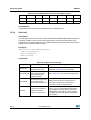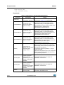
1
UM1634
User manual
Standard software driver for C90FL2 Flash
Introduction
This document is the user manual for the Standard Software Driver (SSD) for C90FL(2)
Flash module.
The SSD is a set of API’s that enables user application to operate on the Flash module
embedded on a microcontroller. The C90FL(2) SSD contains a set of functions to
program/erase C90FL(2) Flash module.
The C90FL(2) Standard Software Driver (SSD) provides the following API’s:
• FlashInit
• FlashErase
• BlankCheck
• FlashProgram
• ProgramVerify
• CheckSum
• FlashSuspend
• FlashResume
• GetLock
• SetLock
• FlashDepletionRecover
• FlashECCLogicCheck
• FlashArrayIntegrityCheck
• FactoryMarginReadCheck
April 2014
DocID024601 Rev 3
1/43
www.st.com
Contents
UM1634
Contents
1
2
Introduction . . . . . . . . . . . . . . . . . . . . . . . . . . . . . . . . . . . . . . . . . . . . . . . . 6
1.1
Document overview . . . . . . . . . . . . . . . . . . . . . . . . . . . . . . . . . . . . . . . . . . 6
1.2
Features . . . . . . . . . . . . . . . . . . . . . . . . . . . . . . . . . . . . . . . . . . . . . . . . . . . 6
Memory layout . . . . . . . . . . . . . . . . . . . . . . . . . . . . . . . . . . . . . . . . . . . . . . 7
2.1
3
General overview . . . . . . . . . . . . . . . . . . . . . . . . . . . . . . . . . . . . . . . . . . . . 7
API specification . . . . . . . . . . . . . . . . . . . . . . . . . . . . . . . . . . . . . . . . . . . . 9
3.1
General overview . . . . . . . . . . . . . . . . . . . . . . . . . . . . . . . . . . . . . . . . . . . . 9
3.2
General type definitions . . . . . . . . . . . . . . . . . . . . . . . . . . . . . . . . . . . . . . . 9
3.3
Configuration parameters and macros . . . . . . . . . . . . . . . . . . . . . . . . . . . . 9
3.4
Callback notification . . . . . . . . . . . . . . . . . . . . . . . . . . . . . . . . . . . . . . . . . 10
3.5
Return codes . . . . . . . . . . . . . . . . . . . . . . . . . . . . . . . . . . . . . . . . . . . . . . .11
3.6
Normal mode functions . . . . . . . . . . . . . . . . . . . . . . . . . . . . . . . . . . . . . . 12
3.7
3.6.1
FlashInit() . . . . . . . . . . . . . . . . . . . . . . . . . . . . . . . . . . . . . . . . . . . . . . . . 12
3.6.2
FlashErase() . . . . . . . . . . . . . . . . . . . . . . . . . . . . . . . . . . . . . . . . . . . . . 13
3.6.3
BlankCheck() . . . . . . . . . . . . . . . . . . . . . . . . . . . . . . . . . . . . . . . . . . . . . 15
3.6.4
FlashProgram() . . . . . . . . . . . . . . . . . . . . . . . . . . . . . . . . . . . . . . . . . . . 17
3.6.5
ProgramVerify() . . . . . . . . . . . . . . . . . . . . . . . . . . . . . . . . . . . . . . . . . . . 19
3.6.6
CheckSum() . . . . . . . . . . . . . . . . . . . . . . . . . . . . . . . . . . . . . . . . . . . . . . 21
3.6.7
FlashSuspend() . . . . . . . . . . . . . . . . . . . . . . . . . . . . . . . . . . . . . . . . . . . 22
3.6.8
FlashResume() . . . . . . . . . . . . . . . . . . . . . . . . . . . . . . . . . . . . . . . . . . . 24
3.6.9
GetLock() . . . . . . . . . . . . . . . . . . . . . . . . . . . . . . . . . . . . . . . . . . . . . . . 25
3.6.10
SetLock()
3.6.11
FlashDepletionRecover() . . . . . . . . . . . . . . . . . . . . . . . . . . . . . . . . . . . . 29
. . . . . . . . . . . . . . . . . . . . . . . . . . . . . . . . . . . . . . . . . . . . . . . 28
User test mode functions . . . . . . . . . . . . . . . . . . . . . . . . . . . . . . . . . . . . . 31
3.7.1
FlashArrayIntegrityCheck() . . . . . . . . . . . . . . . . . . . . . . . . . . . . . . . . . . 31
3.7.2
FlashECCLogicCheck() . . . . . . . . . . . . . . . . . . . . . . . . . . . . . . . . . . . . . 34
3.7.3
FactoryMarginReadCheck() . . . . . . . . . . . . . . . . . . . . . . . . . . . . . . . . . 35
Appendix A System requirements . . . . . . . . . . . . . . . . . . . . . . . . . . . . . . . . . . . . 39
Appendix B Acronyms . . . . . . . . . . . . . . . . . . . . . . . . . . . . . . . . . . . . . . . . . . . . . . 40
2/43
DocID024601 Rev 3
UM1634
Contents
Appendix C Document reference . . . . . . . . . . . . . . . . . . . . . . . . . . . . . . . . . . . . . 41
Revision history . . . . . . . . . . . . . . . . . . . . . . . . . . . . . . . . . . . . . . . . . . . . . . . . . . . . 42
DocID024601 Rev 3
3/43
List of tables
UM1634
List of tables
Table 1.
Table 2.
Table 3.
Table 4.
Table 5.
Table 6.
Table 7.
Table 8.
Table 9.
Table 10.
Table 11.
Table 12.
Table 13.
Table 14.
Table 15.
Table 16.
Table 17.
Table 18.
Table 19.
Table 20.
Table 21.
Table 22.
Table 23.
Table 24.
Table 25.
Table 26.
Table 27.
Table 28.
Table 29.
Table 30.
Table 31.
Table 32.
Table 33.
Table 34.
Table 35.
Table 36.
Table 37.
Table 38.
Table 39.
Table 40.
Table 41.
Table 42.
Table 43.
Table 44.
Table 45.
Table 46.
Table 47.
Table 48.
4/43
Block Information for user . . . . . . . . . . . . . . . . . . . . . . . . . . . . . . . . . . . . . . . . . . . . . . . . . . . 8
Type definitions. . . . . . . . . . . . . . . . . . . . . . . . . . . . . . . . . . . . . . . . . . . . . . . . . . . . . . . . . . . 9
SSD configuration structure field definition . . . . . . . . . . . . . . . . . . . . . . . . . . . . . . . . . . . . . 10
Return codes . . . . . . . . . . . . . . . . . . . . . . . . . . . . . . . . . . . . . . . . . . . . . . . . . . . . . . . . . . . 11
Arguments for FlashInit() . . . . . . . . . . . . . . . . . . . . . . . . . . . . . . . . . . . . . . . . . . . . . . . . . . 12
Return values for FlashInit() . . . . . . . . . . . . . . . . . . . . . . . . . . . . . . . . . . . . . . . . . . . . . . . . 12
Arguments for FlashErase() . . . . . . . . . . . . . . . . . . . . . . . . . . . . . . . . . . . . . . . . . . . . . . . . 13
Return values for FlashErase() . . . . . . . . . . . . . . . . . . . . . . . . . . . . . . . . . . . . . . . . . . . . . . 14
Bit allocation for blocks in low address space . . . . . . . . . . . . . . . . . . . . . . . . . . . . . . . . . . 14
Bit allocation for blocks in middle address space . . . . . . . . . . . . . . . . . . . . . . . . . . . . . . . . 14
Bit allocation for blocks in high address space . . . . . . . . . . . . . . . . . . . . . . . . . . . . . . . . . . 15
Arguments for BlankCheck(). . . . . . . . . . . . . . . . . . . . . . . . . . . . . . . . . . . . . . . . . . . . . . . . 15
Return values for BlankCheck() . . . . . . . . . . . . . . . . . . . . . . . . . . . . . . . . . . . . . . . . . . . . . 16
Arguments for FlashProgram() . . . . . . . . . . . . . . . . . . . . . . . . . . . . . . . . . . . . . . . . . . . . . . 17
Return values for FlashProgram() . . . . . . . . . . . . . . . . . . . . . . . . . . . . . . . . . . . . . . . . . . . 18
Programming algorithm for FlashProgram() . . . . . . . . . . . . . . . . . . . . . . . . . . . . . . . . . . . . 19
Arguments for ProgramVerify() . . . . . . . . . . . . . . . . . . . . . . . . . . . . . . . . . . . . . . . . . . . . . . 19
Return values for ProgramVerify() . . . . . . . . . . . . . . . . . . . . . . . . . . . . . . . . . . . . . . . . . . . 20
Arguments for CheckSum() . . . . . . . . . . . . . . . . . . . . . . . . . . . . . . . . . . . . . . . . . . . . . . . . 21
Return values for CheckSum() . . . . . . . . . . . . . . . . . . . . . . . . . . . . . . . . . . . . . . . . . . . . . . 21
Arguments for FlashSuspend() . . . . . . . . . . . . . . . . . . . . . . . . . . . . . . . . . . . . . . . . . . . . . . 22
Return values for FlashSuspend() . . . . . . . . . . . . . . . . . . . . . . . . . . . . . . . . . . . . . . . . . . . 22
suspendState definitions. . . . . . . . . . . . . . . . . . . . . . . . . . . . . . . . . . . . . . . . . . . . . . . . . . . 23
Suspending state and flag vs. C90FL status . . . . . . . . . . . . . . . . . . . . . . . . . . . . . . . . . . . 23
Arguments for FlashResume() . . . . . . . . . . . . . . . . . . . . . . . . . . . . . . . . . . . . . . . . . . . . . . 24
Return values for FlashResume() . . . . . . . . . . . . . . . . . . . . . . . . . . . . . . . . . . . . . . . . . . . . 25
resumeState definitions . . . . . . . . . . . . . . . . . . . . . . . . . . . . . . . . . . . . . . . . . . . . . . . . . . . 25
Arguments for GetLock() . . . . . . . . . . . . . . . . . . . . . . . . . . . . . . . . . . . . . . . . . . . . . . . . . . 26
Return values for GetLock() . . . . . . . . . . . . . . . . . . . . . . . . . . . . . . . . . . . . . . . . . . . . . . . . 26
blkLockIndicator definitions. . . . . . . . . . . . . . . . . . . . . . . . . . . . . . . . . . . . . . . . . . . . . . . . . 26
blkLockState bit allocation for shadow address space . . . . . . . . . . . . . . . . . . . . . . . . . . . . 27
blkLockState bit allocation for low address space . . . . . . . . . . . . . . . . . . . . . . . . . . . . . . . 27
blkLockState bit allocation for mid address space . . . . . . . . . . . . . . . . . . . . . . . . . . . . . . . 27
blkLockState bit allocation for high address space . . . . . . . . . . . . . . . . . . . . . . . . . . . . . . . 28
Arguments for SetLock() . . . . . . . . . . . . . . . . . . . . . . . . . . . . . . . . . . . . . . . . . . . . . . . . . . . 28
Return values for SetLock() . . . . . . . . . . . . . . . . . . . . . . . . . . . . . . . . . . . . . . . . . . . . . . . . 29
Arguments for FlashDepletionRecover() . . . . . . . . . . . . . . . . . . . . . . . . . . . . . . . . . . . . . . 30
Return values for FlashDepletionRecover() . . . . . . . . . . . . . . . . . . . . . . . . . . . . . . . . . . . . 31
Arguments for FlashArrayIntegrityCheck() . . . . . . . . . . . . . . . . . . . . . . . . . . . . . . . . . . . . . 32
Return values for FlashArrayIntegrityCheck(). . . . . . . . . . . . . . . . . . . . . . . . . . . . . . . . . . . 33
Bit allocation for blocks in low address space . . . . . . . . . . . . . . . . . . . . . . . . . . . . . . . . . . 33
Bit allocation for blocks in middle address space . . . . . . . . . . . . . . . . . . . . . . . . . . . . . . . . 33
Bit Allocation for Blocks in High Address Space. . . . . . . . . . . . . . . . . . . . . . . . . . . . . . . . . 33
Arguments for FlashECCLogicCheck(). . . . . . . . . . . . . . . . . . . . . . . . . . . . . . . . . . . . . . . . 34
Return values for FlashECCLogicCheck() . . . . . . . . . . . . . . . . . . . . . . . . . . . . . . . . . . . . . 35
Arguments for FactoryMarginReadCheck() . . . . . . . . . . . . . . . . . . . . . . . . . . . . . . . . . . . . 36
Return values for FactoryMarginReadCheck() . . . . . . . . . . . . . . . . . . . . . . . . . . . . . . . . . . 37
Bit allocation for blocks in low address space . . . . . . . . . . . . . . . . . . . . . . . . . . . . . . . . . . 37
DocID024601 Rev 3
UM1634
Table 49.
Table 50.
Table 51.
Table 52.
Table 53.
List of tables
Bit allocation for blocks in middle address space . . . . . . . . . . . . . . . . . . . . . . . . . . . . . . . . 37
Bit allocation for blocks in high address space . . . . . . . . . . . . . . . . . . . . . . . . . . . . . . . . . . 38
System requirements . . . . . . . . . . . . . . . . . . . . . . . . . . . . . . . . . . . . . . . . . . . . . . . . . . . . . 39
Acronyms . . . . . . . . . . . . . . . . . . . . . . . . . . . . . . . . . . . . . . . . . . . . . . . . . . . . . . . . . . . . . . 40
Document revision history . . . . . . . . . . . . . . . . . . . . . . . . . . . . . . . . . . . . . . . . . . . . . . . . . 42
DocID024601 Rev 3
5/43
Introduction
UM1634
1
Introduction
1.1
Document overview
This document is the user manual for the Standard Software Driver (SSD) for C90FL(2)
Flash module. The roadmap for the document is as follows.
Section 1.2 shows the features of the driver. Appendix A: System requirements details the
system requirement for the driver development. Appendix C: Document reference lists the
documents referred and Appendix B: Acronyms lists the acronyms used.
Chapter 2 provides information about physical and logical memory map.
Chapter 3 describes the API specifications. In this section there are many sub sections,
which describe the different aspects of the driver. Section 3.1 provides a general overview of
the driver. Section 3.2 talks about the type definitions used for the driver. Section 3.3
discusses about the driver configuration parameters and configuration macros, respectively.
Section 3.4, and Section 3.5 describe the CallBack notifications and return codes used for
the driver. Section 3.6 provides the detailed description of standard software Flash Driver
APIs’.
1.2
Features
The C90FL(2) Standard Software Driver (SSD) provides the following features:
6/43
•
Two sets of driver binaries built on Power Architecture instruction set technology and
Variable-Length-Encoding (VLE) instruction set.
•
Drivers released in binary c-array format to provide compiler-independent support for
non-debug-mode embedded applications.
•
Each driver function is independent of each other so the end user can choose the
function subset to meet their particular needs.
•
Position-independent and ROM-able
•
Concurrency support via callback
DocID024601 Rev 3
UM1634
Memory layout
2
Memory layout
2.1
General overview
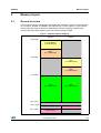
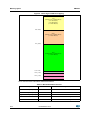
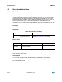
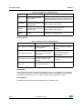
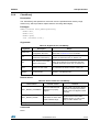
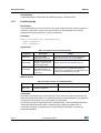
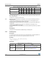
The SPC564Axx microcontrollers has 2 separate flash modules, which can be described as
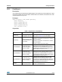
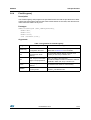
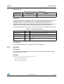
set of 2 banks, BANK0 and BANK1 with separate set of flash registers. Figures below
demonstrate how physical address of SPC564Axx has been mapped to logical linear
memory and same linear mapping has been used to develop the SSD.
Figure 1. Physical address mapping
%$1.
[[B
%$1.
/$6
;.%ORFNV
;.%ORFNV
0$6
;.%ORFNV
[[B
/$6
;.%ORFNV
0$6
;.%ORFNV
[[B
+$6
;.%ORFNV
+$6
;.%ORFNV
[[)B))))
[[()B&
[[))B&
6KDGRZ5RZ
6KDGRZ5RZ
DocID024601 Rev 3
7/43
Memory layout
UM1634
Figure 2. Linear logical address mapping
[[ /$6
%$1./$6%$1.0$6
;.%ORFNV
;.%ORFNV
;.%ORFNV
[[ 0$6
%$1./$6%$1.0$6
;.%ORFNV
[[B
+$6
%$1.+$6%$1.+$6
;.%ORFNV
[[) ))))
[[()B&
6KDGRZ5RZ
[[))B&
6KDGRZ5RZ
So for user the block information looks like as follows:
Table 1. Block Information for user
8/43
Address space
Number of blocks
Description
Low Address Space (LAS)
12
8 x 16K Blocks, 2 x 64K Blocks, 2 x128 k blocks
Mid Address Space (MAS)
2
2 x 256K Blocks
High Address Space (HAS)
6
6 x 512K Blocks
Shadow Row 1
1
Size : 16 K Base address : xxEF_C000
Shadow Row 0
1
Size : 16 K Base address : xxFF_C000
DocID024601 Rev 3
UM1634
API specification
3
API specification
3.1
General overview
The C90FL(2) SSD has APIs to handle the erase, program, erase verify and program verify
operations on the Flash. Apart from these, it also provides the feature for locking specific
blocks and calculating check sum.
3.2
General type definitions
Table 2. Type definitions
Derived type
3.3
Size
C language type description
BOOL
8-bits
unsigned char
INT8
8-bits
signed char
VINT8
8-bits
volatile signed char
UINT8
8-bits
unsigned char
VUINT8
8-bits
volatile unsigned char
INT16
16-bits
signed short
VINT16
16-bits
volatile signed short
UINT16
16-bits
unsigned short
VUINT16
16-bits
volatile unsigned short
INT32
32-bits
signed long
VINT32
32-bits
volatile signed long
UINT32
32-bits
unsigned long
VUINT32
32-bits
volatile unsigned long
INT64
64-bits
signed long long
VINT64
64-bits
volatile signed long long
UINT64
64-bits
unsigned long long
VUINT64
64-bits
volatile unsigned long long
Configuration parameters and macros
The configuration parameters, which are used for SSD operations, are explained in this
section. The configuration parameters are handled as a structure. The user should correctly
initialize the fields including c90flRegBase, mainArrayBase, shadowRowBase,
shadowRowSize, pageSize and BDMEnable before passing the structure to the SSD
functions. The pointer to CallBack has to be initialized either to a null pointer or a valid
function pointer.
DocID024601 Rev 3
9/43
API specification
UM1634
Table 3. SSD configuration structure field definition
Parameter name
Type
Parameter description
c90flRegBase
UINT32
The base address of C90FL and BIU control registers.
(Bank0 base address)
mainArrayBase
UINT32
The base address of Flash main array. (Bank0 base address)
mainArraySize
UINT32
The size of Flash main array.
shadowRowBase
UINT32
The base address of shadow row. (Base Address of shadow
row0 (Bank0 shadow row))
shadowRowSize
UINT32
The size of shadow row in byte.
lowBlockNum
UINT32
Block number of the low address space.
midBlockNum
UINT32
Block number of the mid address space.
highBlockNum
UINT32
Block number of the high address space.
pageSize
UINT16
The page size of the C90FL Flash (16 bytes)
BDMEnable
UINT32
Defines the state of background debug mode (enable
/disable)
The type definition for the structure is given below.
typedef struct _ssd_config
{
UINT32 c90flRegBase;
UINT32 mainArrayBase;
UINT32 mainArraySize;
UINT32 shadowRowBase;
UINT32 shadowRowSize;
UINT32 lowBlockNum;
UINT32 midBlockNum;
UINT32 highBlockNum;
UINT16 pageSize;
UINT32 BDMEnable;
} SSD_CONFIG, *PSSD_CONFIG;
Note:
User has to make sure shadowRowBase always points to Shadow row Base of Bank 0.
Even if the operation is done on Shadow Row of Bank 1, shadowRowBase should have
address of Bank 0 shadow row. Driver code expects shadow row base address of bank 0
only. Driver has the workaround to point to shadow row base of bank 1 when needed (this is
done based on the value set for shadowFlag by the user).
3.4
Callback notification
The Standard Software Driver facilitates the user to supply a pointer to ‘CallBack()’ function
so that time-critical events can be serviced during C90FL Standard Software driver
operations.
Servicing watchdog timers is one such time critical event. If it is not necessary to provide the
CallBack service, the user is able to disable it by a NULL function macro.
10/43
DocID024601 Rev 3
UM1634
API specification
#define NULL_CALLBACK ((void *) 0xFFFFFFFF)
The job processing callback notifications shall have no parameters and no return value.
3.5
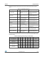
Return codes
The return code is returned to the caller function to notify the success or errors of the API
execution. These are the possible values of return code:
Table 4. Return codes
Name
Value
Description
C90FL_OK
0x00000000
The requested operation is successful.
C90FL_INFO_RWE
0x00000001
RWE bit is set before Flash operations.
C90FL_INFO_EER
0x00000002
EER bit is set before Flash operations.
C90FL_ERROR_ALIGNMENT
0x00000100
Alignment error.
C90FL_ERROR_RANGE
0x00000200
Address range error.
C90FL_ERROR_BUSY
0x00000300
New program/erase cannot be preformed
while a high voltage operation is already in
progress.
C90FL_ERROR_PGOOD
0x00000400
The program operation is unsuccessful.
C90FL_ERROR_EGOOD
0x00000500
The erase operation is unsuccessful.
C90FL_ERROR_NOT_BLANK
0x00000600
There is a non-blank Flash memory location
within the checked Flash memory region.
C90FL_ERROR_VERIFY
0x00000700
There is a mismatch between the source
data and the content in the checked Flash
memory.
C90FL_ERROR_LOCK_INDICATOR 0x00000800
Invalid block lock indicator.
C90FL_ERROR_RWE
0x00000900
Read-while-write error occurred in previous
reads.
C90FL_ERROR_PASSWORD
0x00000A00
The password provided cannot unlock the
block lock register for register writes
C90FL_ERROR_AIC_MISMATCH
0x00000B00
In ‘FlashArrayIntegrityCheck()’ the MISR
values generated by the hardware do not
match the values passed by the user.
C90FL_ERROR_AIC_NO_BLOCK
0x00000C00
In ‘FlashArrayIntegrityCheck()’ no blocks
have been enabled for Array Integrity check
C90FL_ERROR_FMR_MISMATCH
0x00000D00
In ‘FactoryMarginReadCheck()’ the MISR
values generated by the hardware do not
match the values passed by the user.
C90FL_ERROR_FMR_NO_BLOCK
0x00000E00
In ‘FactoryMarginReadCheck()’ no blocks
have been enabled for Array Integrity check
C90FL_ERROR_ECC_LOGIC
0x00000F00
In ‘FlashECCLogicCheck()’ the simulated
ECC error has not occurred.
DocID024601 Rev 3
11/43
API specification
UM1634
3.6
Normal mode functions
3.6.1
FlashInit()
Description
The 'FlashInit()' API reads the Flash configuration information from the Flash control
registers and initialize parameters in SSD configuration structure. The user gets low block
number as sum of LAS and MAS blocks of bank0, mid block number as sum of LAS and
MAS blocks of bank1, high block number remains the same as the high blocks in bank0 or
bank1. Two HAS blocks (one each from Bank0 and Bank1 (size 256 KB each)) are
combined to form one logical HAS block (512 KB). Main array size is returned to the user as
sum of the size of the 2 banks. 'FlashInit()' must be called prior to any other flash operations
Prototype
UINT32 FlashInit (PSSD_CONFIG pSSDConfig);
Arguments
Table 5. Arguments for FlashInit()
Argument
pSSDConfig
Description
Pointer to the SSD
Configuration Structure.
Range
The values in this structure are chip-dependent.
Please refer to Section 3.3 for more details.
Return values
Table 6. Return values for FlashInit()
Return Values
C90FL_OK
Possible Causes
Solution
Successful completion
Comments
The 'FlashInit()' will check the C90FL_MCR_RWE and C90FL_MCR_EER bits, and clear
them when any of them is set.
Assumptions
The user must correctly initialize the fields including c90flRegBase, mainArrayBase,
shadowRowBase, shadowRowSize, pageSize and BDMEnable before passing the structure
to the FlashInit() functions.
12/43
DocID024601 Rev 3
UM1634
3.6.2
API specification
FlashErase()
Description
The 'FlashErase()' API erases the enabled blocks in the main array or the shadow row. Input
arguments together with relevant Flash module status are checked, and relevant error code
is returned if there is any error
Prototype
UINT32 FlashErase (PSSD_CONFIG pSSDConfig,
UINT8 shadowFlag,
UINT32 lowEnabledBlocks,
UINT32 midEnabledBlocks,
UINT32 highEnabledBlocks,
void (*CallBack)(void));
Arguments
Table 7. Arguments for FlashErase()
Argument
Description
Range
pSSDConfig
Pointer to the SSD
The values in this structure are chip-dependent.
Configuration Structure. Please refer to Section 3.3 for more details.
shadowFlag
1: shadow row not to be erased.
2: shadow row of bank0 to be erased i.e. Shadow
Indicate either the main
Row0 to be erased.
array or the shadow row
3: shadow row of bank1 to be erased i.e. Shadow
to be erased.
Row1 to be erased.
4: both the shadow rows to be erased.
lowEnabledBlocks
To select the array
blocks in low address
space for erasing.
Bit-mapped value. Select the block in the low
address space to be erased by setting 1 to the
appropriate bit of lowEnabledBlocks. If there is not
any block to be erased in the low address space,
lowEnabledBlocks must be set to 0.
midEnabledBlocks
To select the array
blocks in mid address
space for erasing.
Bit-mapped value. Select the block in the middle
address space to be erased by setting 1 to the
appropriate bit of midEnabledBlocks. If there is not
any block to be erased in the middle address space,
midEnabledBlocks must be set to 0.
highEnabledBlocks
To select the array
blocks in high address
space for erasing.
Bit-mapped value. Select the block in the high
address space to be erased by setting 1 to the
appropriate bit of highEnabledBlocks. If there is not
any block to be erased in the high address space,
highEnabledBlocks must be set to 0.
CallBack
Address of void call
back function pointer.
Any addressable void function address. To disable it
use NULL_CALLBACK macro.
DocID024601 Rev 3
13/43
API specification
UM1634
Return values
Table 8. Return values for FlashErase()
Return Values
Possible Causes
Solution
Wait until all previous program/erase
operations on this flash module to finish.
New erase operation cannot be
Possible cases that erase cannot start
C90FL_ERROR_B performed because there is
are:
USY
program/erase sequence in
1. erase in progress (MCR-ERS is high);
progress on the same flash module.
2. program in progress (MCR-PGM is
high);
C90FL_ERROR_
EGOOD
Erase operation failed
C90FL_OK
Successful completion
Check if the voltage supplied is sufficient.
Then try to do the erase operation again
Comments
When shadowFlag is set to 0x00, the ‘FlashErase()’ function erases the blocks in the main
array. It is capable of erasing any combination of blocks in the low, mid and high address
spaces in one operation. If shadowFlag is 0x01, 0x02 or 0x03, this function erases the
shadow row of Bank0, Bank1 and Bank0 and Bank1 together respectively. User has to
make sure that security word is programmed back after erasing the shadow rows to protect
the part from getting censored.
The inputs lowEnabledBlocks, midEnabledBlocks and highEnabledBlocks are bit-mapped
arguments that are used to select the blocks to be erased in the Low/Mid/High address
spaces of main array. The selection of the blocks of the main array is determined by
setting/clearing the corresponding bit in lowEnabledBlocks, midEnabledBlocks or
highEnabledBlocks.
The bit allocations for blocks in one address space are: bit 0 is assigned to block 0, bit 1 to
block 1, etc. The following diagrams show the formats of lowEnabledBlocks,
midEnabledBlocks and highEnabledBlocks for the C90FL module.
For low address space valid bits are from bit 0 to bit 9; For middle address space valid bits
are bit 0 and bit 1; For high address space valid bits are from bit 0 to bit 5.
Table 9. Bit allocation for blocks in low address space
MSB
LSB
bit 31
…
bit 10
bit 9
bit 8
…
bit 1
bit 0
reserved
…
reserved
block 9
block 8
…
block 1
block 0
Table 10. Bit allocation for blocks in middle address space
MSB
14/43
LSB
bit 31
…
bit 4
bit 3
bit 2
bit 1
bit 0
reserved
…
reserved
reserved
reserved
block 1
block 0
DocID024601 Rev 3
UM1634
API specification
Table 11. Bit allocation for blocks in high address space
MSB
LSB
bit 31
…
bit 6
bit 5
bit 4
…
bit 1
bit 0
reserved
…
reserved
block 5
block 4
…
Block 1
Block 0
If the selected main array blocks or the shadow row is locked for erasing, those blocks or
the shadow row are not erased, but ‘FlashErase()’ still returns C90FL_OK. User needs to
check the erasing result with the ‘BlankCheck()’ function.
It is impossible to erase any Flash block or shadow row when a program or erase operation
is already in progress on C90FL module. ‘FlashErase()’ returns C90FL_ERROR_BUSY
when trying to do so. Similarly, once an erasing operation has started on C90FL module, it is
impossible to run another program or erase operation.
In addition, when ‘FlashErase()’ is running, it is unsafe to read the data from the Flash
partitions having one or more blocks being erased. Otherwise, it causes a Read-While-Write
error.
Assumptions
It assumes that the Flash block is initialized using a ‘FlashInit()’ API. User provides the
correct ssdconfig parameters to FlashErase() as returned by FlashInit().
3.6.3
BlankCheck()
Description
The 'BlankCheck()' API checks on the specified Flash range in the main array or shadow
row for blank state. If the blank checking fails, the first failing address and the failing data in
Flash block are saved.
Prototype
UINT32 BlankCheck (PSSD_CONFIG pSSDConfig,
UINT32 dest,
UINT32 size,
UINT32 *pFailAddress,
UINT64 *pFailData,
void (*CallBack) (void ));
Arguments
Table 12. Arguments for BlankCheck()
Argument
Description
Range
pSSDConfig
Pointer to the SSD
Configuration Structure.
The values in this structure are chip-dependent.
Please refer to Section 3.3 for more details.
dest
Destination address to be
checked.
Any accessible address aligned on double word
boundary in main array or shadow row
DocID024601 Rev 3
15/43
API specification
UM1634
Table 12. Arguments for BlankCheck()
Argument
Description
Range
If size = 0, the return value is C90FL_OK.
It should be multiple of 8 and its combination with
dest should fall in either main array or shadow row.
size
Size, in bytes, of the Flash
region to check.
pFailAddress
Return the address of the first
Only valid when this function returns
non-blank Flash location in the
C90FL_ERROR_NOT_BLANK.
checking region.
pFailData
Return the content of the first
Only valid when this function returns
non-blank Flash location in the
C90FL_ERROR_NOT_BLANK.
checking region.
CallBack
Address of void callback
function.
Any addressable void function address. To disable
it use NULL_CALLBACK macro.
Return values
Table 13. Return values for BlankCheck()
Return Values
Possible Causes
Solution
C90FL_ERROR_ALIGNMENT
The dest and size are not
properly aligned.
Check if dest and size are
aligned on double word (64-bit)
boundary.
C90FL_ERROR_RANGE
The area specified by dest and
size is out of the valid C90FL
array ranges.
Check dest and dest+size. The
area to be checked must be
within main array space or
shadow space.
There is a non-blank double
C90FL_ERROR_NOT_BLANK word within the area to be
checked.
C90FL_OK
Re-erase the relevant blocks and
check again.
Successful completion.
Comments
If the blank checking fails, the first failing address is saved to *pFailAddress, and the failing
data in Flash is saved to *pFailData. The contents pointed by pFailAddress and pFailData
are updated only when there is a non-blank location in the checked Flash range.
Assumptions
It assumes that the Flash block is initialized using a ‘FlashInit()’ API.
16/43
DocID024601 Rev 3
UM1634
3.6.4
API specification
FlashProgram()
Description
The 'FlashProgram()' API programs the specified Flash areas with the provided source data.
Input arguments together with relevant Flash module status are checked, and relevant error
code is returned if there is any error.
Prototype
UINT32 FlashProgram (PSSD_CONFIG pSSDConfig,
UINT32 dest,
UINT32 size,
UINT32 source,
void (*CallBack)(void));
Arguments
Table 14. Arguments for FlashProgram()
Argument
Description
Range
pSSDConfig
Pointer to the SSD
Configuration Structure.
The values in this structure are chip-dependent.
Please refer to Section 3.3 for more details.
Dest
Destination address to be
programmed in Flash
memory.
Any accessible address aligned on double word
boundary in main array or shadow row.
Size
Size, in bytes, of the Flash
region to be programmed.
If size = 0, C90FL_OK is returned.
It should be multiple of 8 and its combination with dest
should fall in either main array or shadow row.
source
Source program buffer
address.
This address must reside on word boundary.
CallBack
Address of void call back
function pointer.
Any addressable void function address. To disable it
use NULL_CALLBACK macro.
DocID024601 Rev 3
17/43
API specification
UM1634
Return values
Table 15. Return values for FlashProgram()
Return Values
Possible Causes
Solution
– Wait until the current operations finish.
– Use ProgramVerify() API to find:
- The first address in FLASH which has
NOT been programmed as expected in FlashProgram() API.
New program operation
-The first address in SOURCE buffer
cannot be performed
which has NOT been programmed as
because the flash module is
expected in FlashProgram() API.
C90FL_ERROR_BUSY busy with some operation
– Program the rest of data based the new
and cannot meet the
addresses.
condition for starting a
program operation.
Conditions that program cannot start are:
1. program in progress (MCR-PGM high);
2. program not in progress (MCR-PGM low),
but:
a) erase in progress but not suspended
C90FL_ERROR_ALIG
NMENT
This error indicates that
dest/size/source isn’t
properly aligned
Check if dest and size are aligned on double
word (64-bit) boundary. Check if source is
aligned on word boundary
The area specified by dest
C90FL_ERROR_RANG
and size is out of the valid
E
C90FL address range.
Check dest and dest+size. Both should fall in
the same C90FL address ranges, i.e. both in
main array or both in shadow row
C90FL_ERROR_PGO
OD
Program operation failed.
Re-erase relevant location and do
programming again. If still fails, check if the
power supplied is sufficient or not.
C90FL_OK
Successful completion.
Comments
If the selected main array blocks or the shadow row is locked for programming, those blocks
or the shadow row are not programmed, and ‘FlashProgram()’ still returns C90FL_OK. User
needs to verify the programmed data with ‘ProgramVerify()’ function.
It is impossible to program any Flash block or shadow row when a program or erase
operation is already in progress on C90FL module. ‘FlashProgram()’ returns
C90FL_ERROR_BUSY when doing so. However, user can use the ‘FlashSuspend()’
function to suspend an on-going erase operation on one block to perform a program
operation on another block. An exception is that once the user has begun an erase
operation on the main array or shadow row, it may not be suspended to program the main
array and vice-versa.
It is unsafe to read the data from the Flash partitions having one or more blocks being
programmed when ‘FlashProgram()’ is running. Otherwise, it causes a Read-While-Write
error.
If the address to be programmed by the user lies across the boundaries of LAS, MAS and
HAS, ‘FlashProgram()’ handles them as follows:
18/43
DocID024601 Rev 3
UM1634
API specification
Table 16. Programming algorithm for FlashProgram()
Address space to be
programmed
Description
LAS or MAS or Shadow Row
Programmed linearly double word by double word.
HAS
Programmed linearly double word by double word alternately
across each bank.
LAS and MAS
Programmed in parallel until programming in one address space
finishes. The remaining double words are programmed linearly in
the other address space.
MAS and HAS
Program MAS linearly. Once programming finishes, HAS is
programmed in parallel.
LAS, MAS and HAS
First programmed in parallel for LAS and MAS. Once
programming finishes in both the address spaces, HAS is
programmed in parallel.
Assumptions
It assumes that the Flash block is initialized using a ‘FlashInit()’ API.
3.6.5
ProgramVerify()
Description
The 'ProgramVerify()' API checks if a programmed Flash range matches the corresponding
source data buffer. In case of mismatch, the failed address, destination value and source
value are saved and relevant error code is returned.
Prototype
UINT32 ProgramVerify (PSSD_CONFIG pSSDConfig,
UINT32 dest,
UINT32 size,
UINT32 source,
UINT32 *pFailAddress,
UINT64 *pFailData,
UINT64 *pFailSource,
void (*CallBack)(void));
Arguments
Table 17. Arguments for ProgramVerify()
Argument
Description
Range
pSSDConfig
Pointer to the SSD
Configuration Structure.
The values in this structure are chip-dependent.
Please refer to Section 3.3 for more details.
Dest
Destination address to be
verified in Flash memory.
Any accessible address aligned on double word
boundary in main array or shadow row.
DocID024601 Rev 3
19/43
API specification
UM1634
Table 17. Arguments for ProgramVerify() (continued)
Argument
Description
Range
If size = 0, C90FL_OK is returned. Its combination
with dest should fall within either main array or
shadow row.
Size
Size, in byte, of the Flash
region to verify.
Source
Verify source buffer address. This address must reside on word boundary.
pFailAddress
Return first failing address in Only valid when the function returns
Flash.
C90FL_ERROR_VERIFY.
pFailData
Returns first mismatch data
in Flash.
Only valid when this function returns
C90FL_ERROR_VERIFY.
pFailSource
Returns first mismatch data
in buffer.
Only valid when this function returns
C90FL_ERROR_VERIFY.
CallBack
Address of void call back
function pointer.
Any addressable void function address. To disable it
use NULL_CALLBACK macro.
Return values
Table 18. Return values for ProgramVerify()
Return Values
Possible Causes
Solution
Check if dest and size are
aligned on double word (64-bit)
boundary. Check if source is
aligned on word boundary
C90FL_ERROR_ALIGNMENT
This error indicates that
dest/size/source isn‟t properly
aligned
C90FL_ERROR_RANGE
Check dest and dest+size, both
The area specified by dest and
should fall in the same C90FL
size is out of the valid C90FL
address ranges, i.e. both in main
address range.
array or both in shadow row
C90FL_ERROR_VERIFY
The content in C90FL and
source data mismatch.
C90FL_OK
Successful completion
Check the correct source and
destination addresses, erase the
block and reprogram data into
flash.
Comments
The contents pointed by pFailLoc, pFailData and pFailSource are updated only when there
is a mismatch between the source and destination regions.
Assumptions
It assumes that the Flash block is initialized using a ‘FlashInit()’ API.
20/43
DocID024601 Rev 3
UM1634
3.6.6
API specification
CheckSum()
Description
The 'CheckSum()' API performs a 32-bit sum over the specified Flash memory range
without carry, which provides a rapid method for checking data integrity.
Prototype
UINT32 CheckSum (PSSD_CONFIG pSSDConfig,
UINT32 dest,
UINT32 size,
UINT32 *pSum,
void (*CallBack)(void));
Arguments
Table 19. Arguments for CheckSum()
Argument
Description
Range
pSSDConfig
Pointer to the SSD
Configuration Structure.
The values in this structure are chip-dependent.
Please refer to Section 3.3 for more details.
Dest
Destination address to be
summed in Flash memory.
Any accessible address aligned on double word
boundary in either main array or shadow row.
Size
Size, in bytes, of the Flash
region to check sum.
If size is 0 and the other parameters are all valid,
C90FL_OK is returned. Its combination with dest
should fall within either main array or shadow row.
pSum
Returns the sum value.
0x00000000 - 0xFFFFFFFF. Note that this value is
only valid when the function returns C90FL_OK.
CallBack
Address of void call back
function pointer.
Any addressable void function address. To disable it
use NULL_CALLBACK macro.
Return values
Table 20. Return values for CheckSum()
Return Values
Possible Causes
Solution
C90FL_ERROR_ALIGNMENT
This error indicates that
dest/size isn’t properly
aligned
Check if dest and size are aligned
on double word (64-bit) boundary.
Check if source is aligned on word
boundary
C90FL_ERROR_RANGE
The area specified by dest
and size is out of the valid
C90FL address range.
Check dest and dest+size, both
should fall in the same C90FL
address ranges, i.e. both in main
array or both in shadow row
C90FL_OK
Successful completion.
Comments
None.
DocID024601 Rev 3
21/43
API specification
UM1634
Assumptions
It assumes that the Flash block is initialized using a ‘FlashInit()’ API.
3.6.7
FlashSuspend()
Description
The 'FlashSuspend()' API checks if there is any high voltage operation, erase or program, in
progress on the C90FL module and if the operation can be suspended. This function
suspends the ongoing operation if it can be suspended.
Prototype
UINT32 FlashSuspend (PSSD_CONFIG pSSDConfig,
UINT8 *suspendState,
BOOL *suspendFlag);
Arguments
Table 21. Arguments for FlashSuspend()
Argument
Description
Range
pSSDConfig
Pointer to the SSD
Configuration Structure.
The values in this structure are chip-dependent.
Please refer to Section 3.3 for more details.
suspendState
Indicate the suspend state
of C90FL module after the
function being called.
All return values are enumerated inTable 24.
suspendFlag
Return whether the
suspended operation, if
there is any, is suspended
by this call.
TRUE: the operation is suspended by this call;
FALSE: either no operation to be suspended or the
operation is suspended not by this call.
Return values
Table 22. Return values for FlashSuspend()
Return Values
C90FL_OK
Possible Causes
Solution
Successful completion.
Comments
After calling ‘FlashSuspend()’, read is allowed on both main array space and shadow row
without any Read-While-Write error. But data read from the blocks targeted for programming
or erasing is indeterminate even if the operation is suspended.
This function should be used together with ‘FlashResume()’. The suspendFlag returned by
‘FlashSuspend()’ determine whether ‘FlashResume()’ needs to be called or not. If
suspendFlag is TRUE, ‘FlashResume()’ must be called symmetrically to resume the
suspended operation.
22/43
DocID024601 Rev 3
UM1634
API specification
Following table defines and describes various suspend states and associated suspend
codes.
Table 23. suspendState definitions
Argument
Code
Description
Valid operation after suspend
Erasing operation, programming
operation and read are valid on
both main array space and
shadow row.
Only read is valid on both main
array space and shadow row.
NO_OPERTION
0
There is no program/erase
operation.
PGM_WRITE
1
There is a program
sequence in interlock write
stage.
ERS_WRITE
2
There is an erase sequence Only read is valid on both main
in interlock write stage.
array space and shadow row.
ERS_SUS_PGM_WRITE
3
There is an erase-suspend
program sequence in
interlock write stage.
Only read is valid on both main
array space and shadow row.
PGM_SUS
4
The program operation is in
suspended state.
Only read is valid on both main
array space and shadow row.
ERS_SUS
5
The erase operation on
main array is in suspended
state.
Programming operation is valid
only on main array space. Read
is valid on both main array space
and shadow row.
SHADOW_ERS_SUS
6
The erase operation on
Read is valid on both main array
shadow row is in suspended
space and shadow space.
state.
ERS_SUS_PGM_SUS
7
The erase-suspended
program operation is in
suspended state.
Only read is valid on both main
array space and shadow row.
The table below lists the Suspend Flag values returned against the Suspend State and the
Flash block status.
Table 24. Suspending state and flag vs. C90FL status
suspendState
EHV
ERS
ESUS
PGM
PSUS
PEAS
suspendFlag
NO_OPERATION
X
0
X
0
X
X
FALSE
PGM_WRITE
0
0
X
1
0
X
FALSE
ERS_WRITE
0
1
0
0
X
X
FALSE
ESUS_PGM_WRITE
0
1
1
1
0
X
FALSE
1
0
X
1
0
X
TRUE
X
0
X
1
1
X
FALSE
1
1
0
0
X
0
TRUE
X
1
1
0
X
0
FALSE
PGM_SUS
ERS_SUS
DocID024601 Rev 3
23/43
API specification
UM1634
Table 24. Suspending state and flag vs. C90FL status (continued)
suspendState
EHV
ERS
ESUS
PGM
PSUS
PEAS
suspendFlag
1
1
0
0
X
1
TRUE
X
1
1
0
X
1
FALSE
1
1
1
1
0
X
TRUE
X
1
1
1
1
X
FALSE
SHADOW_ERS_SUS
ERS_SUS_PGM_SUS
The values of EHV, ERS, ESUS, PGM, PSUS and PEAS represent the C90FL status at the
entry of FlashSuspend;
0: Logic zero; 1: Logic one; X: Do-not-care.
Note:
Since there are two Flash banks in SPC564Axx, user can perform following operations in
respective blocks:
— Erase can be suspended in any of the LAS blocks from 0 to 9 and program can be
performed on block 10 and block11 of LAS or vice-versa.
— Erase can be suspended in MAS block 0 and program can be performed in MAS block 1
or vice-versa.
— Erase can be suspended in any of the LAS or MAS blocks and program can be
performed in HAS blocks or vice-versa.
— LAS and MAS blocks can be programmed or erased simultaneously without any suspend
operation.
Assumptions
It assumes that the Flash block is initialized using a ‘FlashInit()’ API.
3.6.8
FlashResume()
Description
The 'FlashResume()' API checks if there is any suspended erase or program operation on
the C90FL module, and resumes the suspended operation if there is any.
Prototype
UINT32 FlashResume (PSSD_CONFIG pSSDConfig,
UINT8 *resumeState);
Arguments
Table 25. Arguments for FlashResume()
Argument
24/43
Description
Range
pSSDConfig
Pointer to the SSD
Configuration Structure.
The values in this structure are chip-dependent.
Please refer to Section 3.3 for more details.
resumeState
Indicate the resume state of
C90FL module after the
All return values are listed in Table 26.
function being called.
DocID024601 Rev 3
UM1634
API specification
Return values
Table 26. Return values for FlashResume()
Return Values
C90FL_OK
Possible Causes
Solution
Successful completion.
Comments
This function resumes one operation if there is any operation is suspended. For instance, if
a program operation is in suspended state, it is resumed. If an erase operation is in
suspended state, it is resumed too. If an erase-suspended program operation is in
suspended state, the program operation is resumed prior to resuming the erase operation. It
is better to call this function based on suspendFlag returned from ‘FlashSupend()’.
Following table defines and describes various resume states and associated resume codes.
Table 27. resumeState definitions
Code name
Value
Description
RES_NOTHING
0
No program/erase operation to be resumed
RES_PGM
1
A program operation is resumed
RES_ERS
2
A erase operation is resumed
RES_ERS_PGM
3
A suspended erase-suspended program operation is
resumed
Assumptions
It assumes that the Flash block is initialized using a ‘FlashInit()’ API.
3.6.9
GetLock()
Description
The 'GetLock()' API checks the block locking status of Shadow/Low/Middle/High address
spaces in the C90FL module.
Prototype
UINT32 GetLock (PSSD_CONFIG pSSDConfig,
UINT8 blkLockIndicator,
BOOL *blkLockEnabled,
UINT32 *blkLockState);
DocID024601 Rev 3
25/43
API specification
UM1634
Arguments
Table 28. Arguments for GetLock()
Argument
Description
Range
pSSDConfig
Pointer to the SSD
Configuration Structure.
The values in this structure are chip-dependent.
Please refer to Section 3.3 for more details.
blkLockIndicator
Indicating the address space
and the block locking level,
Refer to Table 30 for valid values for this
which determines the address
parameter.
space block locking register
to be checked.
blkLockEnabled
TRUE – The address space block locking register
Indicate whether the address
is enabled for register writes.
space block locking register is
FALSE – The address space block locking
enabled for register writes
register is disabled for register writes.
blkLockState
Returns the blocks’ locking
status of indicated locking
level in the given address
space
Bit mapped value indicating the locking status of
the specified locking level and address space.
1: The block is locked from program/erase.
0: The block is ready for program/erase
Return values
Table 29. Return values for GetLock()
Return Values
Possible Causes
C90FL_ERROR_LOCK
The input blkLockIndicator is invalid
_INDICATOR
C90FL_OK
Solution
Set this argument to correct value
listed in Table 30
Successful completion
Comments
Following table defines and describes various blkLockIndicator values.
Table 30. blkLockIndicator definitions
Code Name
LOCK_SHADOW_PRIMARY0
26/43
Value
0
Description
Primary block lock protection of shadow address
space. (Shadow row 0)
LOCK_SHADOW_SECONDARY0 1
Secondary block lock protection of shadow address
space. (Shadow row 0)
LOCK_SHADOW_PRIMARY1
Primary block lock protection of shadow address
space. (Shadow row 1)
2
LOCK_SHADOW_SECONDARY1 3
Secondary block lock protection of shadow address
space. (Shadow row 1)
LOCK_LOW_PRIMARY
4
Primary block lock protection of low address space.
LOCK_LOW_SECONDARY
5
Secondary block lock protection of low address space
DocID024601 Rev 3
UM1634
API specification
Table 30. blkLockIndicator definitions (continued)
Code Name
Value
Description
LOCK_MID_PRIMARY
6
Primary block lock protection of mid address space
LOCK_MID_SECONDARY
7
Secondary block lock protection of mid address space
LOCK_HIGH
8
Block lock protection of high address space
For Shadow/Low/Mid address spaces, there are two block lock levels. The secondary level
of block locking provides an alternative means to protect blocks from being modified. A
logical “OR” of the corresponding bits in the primary and secondary lock registers for a block
determines the final lock status for that block. For high address space there is only one
block lock level.
The output parameter blkLockState returns a bit-mapped value indicating the block lock
status of the specified locking level and address space. A main array block or shadow row is
locked from program/erase if its corresponding bit is set.
The indicated address space determines the valid bits of blkLockState. For either
Low/Mid/High address spaces, if blocks corresponding to valid block lock state bits are not
present (due to configuration or total memory size), values for these block lock state bits will
be always 1 because such blocks are locked by hardware on reset. These blocks cannot be
unlocked by software with 'SetLock()' function.
The following diagrams show the block bitmap definitions of blkLockState for
shadow/Low/Mid/High address spaces.
Table 31. blkLockState bit allocation for shadow address space
MSB
LSB
bit 31
reserved
…
bit 1
…
bit 0
reserved
shadow row
Table 32. blkLockState bit allocation for low address space
MSB
LSB
bit 31
…
bit 10
bit 9
bit 8
…
bit 1
bit 0
reserved
…
reserved
block 9
block 8
…
block 1
block 0
Table 33. blkLockState bit allocation for mid address space
MSB
LSB
bit 31
…
bit 4
bit 3
bit 2
bit 1
bit 0
reserved
…
reserved
reserved
reserved
block 1
block 0
DocID024601 Rev 3
27/43
API specification
UM1634
Table 34. blkLockState bit allocation for high address space
MSB
LSB
bit 31
…
bit 6
bit 5
bit 4
…
bit 1
bit 0
reserved
…
reserved
block 5
block 4
…
block 1
block 0
Assumptions
It assumes that the Flash block is initialized using a ‘FlashInit()’ API.
3.6.10
SetLock()
Description
The 'SetLock()' API sets the block lock state for Shadow/Low/Middle/High address space on
the C90FL module to protect them from program/erase. The API provides password to
enable block lock register writes when is needed and write the block lock value to block lock
register for the requested address space.
Prototype
UINT32 SetLock (PSSD_CONFIG pSSDConfig,
UINT8 blkLockIndicator,
UINT32 blkLockState,
UINT32 password);
Arguments
Table 35. Arguments for SetLock()
Argument
Range
pSSDConfig
Pointer to the SSD
Configuration Structure.
The values in this structure are chip-dependent.
Please refer to Section 3.3 for more details.
blkLockIndicator
Indicating the address
space and the protection
level of the block lock
register to be read.
Refer to Table 30 for valid codes for this parameter.
blkLockState
Bit mapped value indicating the lock status of the
The block locks to be set to specified protection level and address space.
the specified address
1: The block is locked from program/erase.
space and protection level.
0: The block is ready for program/erase
password
28/43
Description
A password is required to
enable the block lock
register for register write.
Correct passwords for block lock registers are
0xA1A1_1111 for Low/Mid Address Space Block
Locking Register, 0xC3C3_3333 for Secondary
Low/Mid Address Space Block Locking Register,
and 0xB2B2_2222 for High Address Space Block
Select Register.
DocID024601 Rev 3
UM1634
API specification
Return values
Table 36. Return values for SetLock()
Return Values
Possible Causes
Solution
C90FL_ERROR_LOCK_INDICATOR
The input blkLockIndicator is
invalid.
Set this argument to
correct value listed in
Table 30
C90FL_ERROR_PASSWORD
The given password cannot enable
the block lock register for register
writes.
Pass in a correct
password
C90FL_OK
Successful completion
Comments
The bit field allocation for blkLockState is same as that in ‘GetLock()’ function.
Assumptions
It assumes that the Flash block is initialized using a ‘FlashInit()’ API.
3.6.11
FlashDepletionRecover()
Description
This function recovers over-erased or depleted bits in flash block. It is possible that a
brownout during Flash erase operation will leave the bits in the Flash block(s) being erased
at an over-erased or depleted state. Depending how depleted the bits are, the excessive
column leakage caused by the bits might cause the following erase operation for brownout
recovery to fail due to suppressed drain bias. For such case, this function invok to recover
the depleted bits in those Flash block(s) so that they can be erased again for brownout
recovery.
Prototype
UINT32 FlashDepletionRecover (PSSD_CONFIG pSSDConfig,
UINT8 shadowFlag,
UINT32 lowEnabledBlocks,
UINT32 midEnabledBlocks,
UINT32 highEnabledBlocks,
void (*CallBack)(void));
DocID024601 Rev 3
29/43
API specification
UM1634
Arguments
Table 37. Arguments for FlashDepletionRecover()
Argument
30/43
Description
Range
The values in this structure are chipdependent. Please refer to Section 3.3 for
more details.
pSSDConfig
Pointer to the SSD
Configuration Structure
shadowFlag
04- Shadow row not to be recovered.
05- Shadow row of bank0 to be erased i.e.
Indicate either the main array or Shadow Row0 to be recovered.
the shadow row to be
06- Shadow row of bank1 to be erased i.e.
recovered.
Shadow Row1 to be recovered.
07- Both the shadow rows to be recovered
lowEnabledBlocks
To select the array blocks in
linear logical low address space
Refer to section Arguments, in Section 3.6.2
for recovering (refer to
for details.
Section 2.1: General overview
for more details).
midEnabledBlocks
To select the array blocks in
linear logical mid address space
Refer to section Arguments, in Section 3.6.2
for recovering (refer to
for details.
Section 2.1: General overview
for more details).
highEnabledBlocks
To select the array blocks in
linear logical high address
space for recovering (refer to
Section 2.1: General overview
for more details).
Refer to section Arguments, in Section 3.6.2
for details.
CallBack
Address of void call back
function pointer.
Any addressable void function address. To
disable it, use NULL_CALLBACK macro.
DocID024601 Rev 3
UM1634
API specification
Return values
Table 38. Return values for FlashDepletionRecover()
Return Values
Possible Causes
Solution
Depletion operation cannot
be performed because there
is program/erase sequence
in progress on the flash
module.
Wait until all previous
program/erase operations on
the flash module finish.
Possible cases that erase
cannot start are:
1. erase in progress (MCRERS is high);
2. program in progress (MCRPGM is high)
C90FL_ERROR_ EGOOD
Depletion operation failed.
Check if the C90FL module is
available and high voltage is
applied to C90FL. Then try to
do the recovery operation
again.
C90FL_OK
Successful completion.
C90FL_ERROR_BUSY
Comments
For comments please refer to Section 3.6.2 for details.
Assumptions
It assumes that the flash block is initialized using the FlashInit()’API. User will provide the
correct ssdconfig parameters to the FlashDepletionRecover () as returned by the FlashInit().
3.7
User test mode functions
3.7.1
FlashArrayIntegrityCheck()
Description
This function checks the array integrity of the Flash. The user specified address sequence is
used for array integrity reads and the operation is done on the specified blocks. The MISR
values calculated by the hardware is compared to the values passed by the user, if they are
not the same, then an error code is returned.
Prototype
UINT32 FlashArrayIntegrityCheck (PSSD_CONFIG pSSDConfig,
UINT32 lowEnabledBlocks,
UINT32 midEnabledBlocks,
UINT32 highEnabledBlocks,
UINT8 addrSeq,
MISR misrValue_Bk0,
DocID024601 Rev 3
31/43
API specification
UM1634
MISR misrValue_Bk1,
void (*CallBack)(void));
Arguments
Table 39. Arguments for FlashArrayIntegrityCheck()
Argument
Range
Pointer to the SSD
Configuration Structure.
The values in this structure are chip-dependent.
Please refer to Section 3.3 for more details.
To select the array
blocks in low address
space for erasing.
Bit-mapped value. Select the block in the low
address space whose array integrity is to be
evaluated by setting 1 to the appropriate bit of
lowEnabledBlocks. If there is not any block to be
evaluated in the low address space,
lowEnabledBlocks must be set to 0.
To select the array
blocks in mid address
space for erasing.
Bit-mapped value. Select the block in the middle
address space whose array integrity is to be
evaluated by setting 1 to the appropriate bit of
midEnabledBlocks. If there is not any block to be
evaluated in the middle address space,
midEnabledBlocks must be set to 0.
To select the array
blocks in high address
space for erasing.
Bit-mapped value. Select the block in the high
address space whose array integrity is to be
evaluated by setting 1 to the appropriate bit of
highEnabledBlocks. If there is not any block to be
evaluated in the high address space,
highEnabledBlocks must be set to 0.
addrSeq
To determine the
address sequence to be
used during array
integrity checks.
The default sequence (addrSeq = 0) is meant to
replicate sequences normal “user” code follows,
and thoroughly check the read propagation paths.
This sequence is proprietary.
The alternative sequence (addrSeq = 1) is just
logically sequential.
It should be noted that the time to run a sequential
sequence is significantly shorter than the time to
run the proprietary sequence.
misrValue_Bk0
A structure variable
containing the MISR
values for Bank 0
The individual MISR words can range from
calculated by the user by 0x00000000 - 0xFFFFFFFF
using an off-line MISR
calculator.
misrValue_Bk1
A structure variable
containing the MISR
values for Bank 1
The individual MISR words can range from
calculated by the user by 0x00000000 - 0xFFFFFFFF
using an off-line MISR
calculator.
CallBack
Address of void call back Any addressable void function address. To disable
function pointer.
it use NULL_CALLBACK macro.
pSSDConfig
lowEnabledBlocks
midEnabledBlocks
highEnabledBlocks
32/43
Description
DocID024601 Rev 3
UM1634
API specification
Return values
Table 40. Return values for FlashArrayIntegrityCheck()
Return Values
Possible Causes
Solution
The MISR value calculated
by the user is incorrect.
Re-calculate the MISR values
using the correct Data and
addrSeq.
The MISR calculated by the
Hardware is incorrect.
Hardware Error.
C90FL_ERROR_AIC_NO_BLOCK
None of the Blocks are
enabled for Array Integrity
Check
Enable any of the blocks using
variables lowEnabledBlocks,
midEnabledBlocks and
highEnabledBlock.
C90FL_OK
Successful completion
C90FL_ERROR_AIC_MISMATCH
Comments
The inputs lowEnabledBlocks, midEnabledBlocks and highEnabledBlocks are bit-mapped
arguments that are used to select the blocks to be evaluated in the Low/Mid/High address
spaces of main array. The selection of the blocks of the main array is determined by
setting/clearing the corresponding bit in lowEnabledBlocks, midEnabledBlocks or
highEnabledBlocks.
The bit allocations for blocks in one address space are: bit 0 is assigned to block 0, bit 1 to
block 1, etc. The following diagrams show the formats of lowEnabledBlocks,
midEnabledBlocks and highEnabledBlocks for the C90FL module.
For low address space valid bits are from bit 0 to bit 9; For middle address space valid bits
are bit 0 and bit 1; For high address space valid bits are from bit 0 to bit 5;
Table 41. Bit allocation for blocks in low address space
MSB
LSB
bit 31
…
bit 10
bit 9
bit 8
…
bit 1
bit 0
reserved
…
reserved
block 9
block 8
…
block 1
block 0
Table 42. Bit allocation for blocks in middle address space
MSB
LSB
bit 31
…
bit 4
bit 3
bit 2
bit 1
bit 0
reserved
…
reserved
reserved
reserved
block 1
block 0
Table 43. Bit Allocation for Blocks in High Address Space
MSB
LSB
bit 31
…
bit 6
bit 5
bit 4
…
bit 1
bit 0
reserved
…
reserved
block 5
block 4
…
Block 1
Block 0
DocID024601 Rev 3
33/43
API specification
UM1634
If no blocks are enabled the C90FL_ERROR_AIC_NO_BLOCK error code is returned.
Depending on the address sequence specified the MISR values are calculated for the
enabled blocks using the corresponding sequence. If the MISR values calculated by the
hardware is not the same as the values passed to this API by the user then the API returns
the error code C90FL_ERROR_AIC_MISMATCH.
Assumptions
It assumes that the Flash block is initialized using a ‘FlashInit()’ API.
3.7.2
FlashECCLogicCheck()
Description
This function checks the ECC logic of the Flash. The API simulates a single or double bit
fault depending on the user input. If the simulated ECC error is not detected, then the error
code C90FL_ERROR_ECC_LOGIC is returned. User has to pass ECC value calculated by
the off-line tool to this API.
Prototype
UINT32 FlashECCCLogicCheck (PSSD_CONFIG pSSDConfig,
UINT64 dataVal,
UINT64 errBits,
UINT8 eccValue,
UINT8 errECCBits)
Arguments
Table 44. Arguments for FlashECCLogicCheck()
Argument
34/43
Description
Range
pSSDConfig
Pointer to the SSD
Configuration Structure.
The values in this structure are chip-dependent.
Please refer to Section 3.3 for more details.
dataValue
The 64 bits of data for which
the ECC is calculated. The
bits of dataValue are flipped Any 64-bit value
to generate single or double
bit faults.
errBits
64-bit mask of the bits at
which the user intends to
inject error on data value.
Any 64-bit value. Select the bit to be a fault bit by
setting 1 to the appropriate bit of this input.
eccValue
8 bit ECC value which is
calculated by an offline
ECC calculator.
This is a corresponding ECC value for the data
value passed by the user.
Note: Same data words should be used in offline
ECC calculator and Flash ECC logic check API.
errECCBits
8-bit mask of the bits at
which the user intends to
inject error on ECC value
Any 8-bit value. Select the bit to be a fault bit by
setting 1 to the appropriate bit of this input.
DocID024601 Rev 3
UM1634
API specification
Return values
Table 45. Return values for FlashECCLogicCheck()
Return Values
Possible Causes
C90FL_ERROR_ECC_LOGIC
Solution
The ECC value calculated
by the user is incorrect.
Re-calculate the ECC values
using the correct Data.
Hardware is failure
Hardware Error.
C90FL_ERROR_ECC_NOTCHECK
This API supports to check
There are more than two bit
single bit fault correction or
faults simulated.
double bit fault detection only.
C90FL_OK
Successful completion
Comments
The API supports single bit correction and double bit error detection in 72-bit codeword
including 8 ECC bits. Depending on the errBits and errECCBits values, a single or double bit
faults is simulated. When a Flash read is done, if the simulated error has not occurred, then
the API returns the error code C90FL_ERROR_ECC_LOGIC. For more than two bit faults
detection, the behavior
is indeterministic. Thus, this API will not check for this case and shall return error code
C90FL_ERROR_ECC_NOTCHECK.
The read buffer in flash platform controller must be disabled before simulating for single bit
correction and double bit detection. For double bit detection, the ECC error exception
handler needs to be set up properly as well.
Assumptions
It assumes that the Flash block is initialized using a ‘FlashInit()’ API.
3.7.3
FactoryMarginReadCheck()
Description
This function checks the Factory Margin reads of the Flash. The user specified margin level
is used for reads and the operation is done on the specified blocks. The MISR values
calculated by the hardware is compared to the values passed by the user, if they are not the
same, then an error code is returned.
Prototype
UINT32 FactoryMarginReadCheck (PSSD_CONFIG pSSDConfig,
UINT32 lowEnabledBlocks,
UINT32 midEnabledBlocks,
UINT32 highEnabledBlocks,
UINT8 marginLevel,
MISR misrValue_Bk0,
MISR misrValue_Bk1,
void (*CallBack)(void));
DocID024601 Rev 3
35/43
API specification
UM1634
Arguments
Table 46. Arguments for FactoryMarginReadCheck()
Argument
36/43
Description
Range
pSSDConfig
Pointer to the SSD
Configuration Structure.
The values in this structure are chip-dependent.
Please refer to Section 3.3 for more details.
lowEnabledBlocks
Bit-mapped value. Select the block in the low
address space whose array integrity is to be
To select the array blocks
evaluated by setting 1 to the appropriate bit of
in low address space for
lowEnabledBlocks. If there is not any block to be
erasing.
evaluated in the low address space,
lowEnabledBlocks must be set to 0.
midEnabledBlocks
Bit-mapped value. Select the block in the middle
address space whose array integrity is to be
To select the array blocks
evaluated by setting 1 to the appropriate bit of
in mid address space for
midEnabledBlocks. If there is not any block to be
erasing.
evaluated in the middle address space,
midEnabledBlocks must be set to 0.
highEnabledBlocks
Bit-mapped value. Select the block in the high
address space whose array integrity is to be
To select the array blocks
evaluated by setting 1 to the appropriate bit of
in high address space for
highEnabledBlocks. If there is not any block to be
erasing.
evaluated in the high address space,
highEnabledBlocks must be set to 0.
marginLevel
To determine the margin
level to be used during
factory margin read
checks.
Selects the margin level that is being checked.
Margin can be checked to an erased level
(marginLevel = 1) or to a programmed level
(marginLevel = 0).
misrValue_Bk0
A structure variable
containing the MISR
values for Bank 0
calculated by the user
using an off-line MISR
calculator.
The individual MISR words can range from
0x00000000 - 0xFFFFFFFF
misrValue_Bk1
A structure variable
containing the MISR
values for Bank 1
calculated by the user
using an off-line MISR
calculator.
The individual MISR words can range from
0x00000000 - 0xFFFFFFFF
CallBack
Address of void call back
function pointer.
Any addressable void function address. To disable
it use NULL_CALLBACK macro.
DocID024601 Rev 3
UM1634
API specification
Return values
Table 47. Return values for FactoryMarginReadCheck()
Return Values
Possible Causes
The MISR value calculated
by the user is incorrect.
C90FL_ERROR_FMR_MISMATC
H
Re-calculate the MISR values
using the correct Data and
address.
The MISR calculated by the
Hardware is incorrect.
Hardware Error.
None of the Blocks are
C90FL_ERROR_FMR_NO_BLOC
enabled for Factory Margin
K
Read Check
C90FL_OK
Solution
Enable any of the blocks using
variables
lowEnabledBlocks,
midEnabledBlocks and
highEnabledBlock.
Successful completion
Comments
The inputs lowEnabledBlocks, midEnabledBlocks and highEnabledBlocks are bit-mapped
arguments that are used to select the blocks to be evaluated in the Low/Mid/High address
spaces of main array. The selection of the blocks of the main array is determined by
setting/clearing the corresponding bit in lowEnabledBlocks, midEnabledBlocks or
highEnabledBlocks.
The bit allocations for blocks in one address space are: bit 0 is assigned to block 0, bit 1 to
block 1, etc. The following diagrams show the formats of lowEnabledBlocks,
midEnabledBlocks and highEnabledBlocks for the C90FL module.
For low address space valid bits are from bit 0 to bit 9; for middle address space valid bits
are bit 0 and bit 1; for high address space valid bits are from bit 0 to bit 5.
Table 48. Bit allocation for blocks in low address space
MSB
LSB
bit 31
…
bit 10
bit 9
bit 8
…
bit 1
bit 0
reserved
…
reserved
block 9
block 8
…
block 1
block 0
Table 49. Bit allocation for blocks in middle address space
MSB
LSB
bit 31
…
bit 4
bit 3
bit 2
bit 1
bit 0
reserved
…
reserved
reserved
reserved
block 1
block 0
DocID024601 Rev 3
37/43
API specification
UM1634
Table 50. Bit allocation for blocks in high address space
MSB
LSB
bit 31
…
bit 6
bit 5
bit 4
…
bit 1
bit 0
reserved
…
reserved
block 5
block 4
…
Block 1
Block 0
If no blocks are enabled the C90FL_ERROR_FMR_NO_BLOCK error code is returned.
The MISR values are calculated for the enabled blocks using the logical sequence. If the
MISR values calculated by the hardware is not the same as the values passed to this API by
the user then the API returns the error code C90FL_ERROR_FMR_MISMATCH.
Assumptions
It assumes that the Flash block is initialized using a ‘FlashInit()’ API.
38/43
DocID024601 Rev 3
UM1634
System requirements
Appendix A
System requirements
The C90FL(2) SSD is designed to support C90FL(2) Flash module embedded on
SPC564Axx microcontrollers. Before using this SSD on a different derivative
microcontroller, user has to provide the information specific to the derivative through a
configuration structure.
Table 51. System requirements
Tool name
Description
Version number
CodeWarrior IDE
Development tool
2.3
Win32/Diab
Development tool
5.5.1.0
Trace32/Lauterbach
Debugging tool
DocID024601 Rev 3
—
39/43
Acronyms
UM1634
Appendix B
Acronyms
Table 52. Acronyms
Abbreviation
40/43
Complete name
API
Application Programming Interface
ECC
Error Correction Code
ECU
Electronic Control Unit
EVB
Evaluation Board
RWW
Read While Write
SSD
Standard Software Driver
DocID024601 Rev 3
UM1634
Document reference
Appendix C
1.
Document reference
SPC564A74xx, SPC564A80xx 32-bit MCU family built on the embedded Power
Architecture® (RM0029, DocID15177)
DocID024601 Rev 3
41/43
Revision history
UM1634
Revision history
Table 53. Document revision history
Date
Revision
02-May-2013
1
Initial release.
22-Sep-2013
2
Updated Disclaimer.
3
– Add FlashDepletionRecover()
– Remove note about COMPILER_SELECT in Section 3.3:
Configuration parameters and macros
– Merge Return Values table and Troubleshooting table for
Section 3: API specification
– Add more information in comment section of
FlashECCLogicCheck
– Change function prototype of FlashECCLogicCheck.
– Add one more return value C90FL_ERROR_ECC_NOTCHECK
for FlashECCLogicCheck
09-Apr-2014
42/43
Changes
DocID024601 Rev 3
UM1634
Please Read Carefully:
Information in this document is provided solely in connection with ST products. STMicroelectronics NV and its subsidiaries (“ST”) reserve the
right to make changes, corrections, modifications or improvements, to this document, and the products and services described herein at any
time, without notice.
All ST products are sold pursuant to ST’s terms and conditions of sale.
Purchasers are solely responsible for the choice, selection and use of the ST products and services described herein, and ST assumes no
liability whatsoever relating to the choice, selection or use of the ST products and services described herein.
No license, express or implied, by estoppel or otherwise, to any intellectual property rights is granted under this document. If any part of this
document refers to any third party products or services it shall not be deemed a license grant by ST for the use of such third party products
or services, or any intellectual property contained therein or considered as a warranty covering the use in any manner whatsoever of such
third party products or services or any intellectual property contained therein.
UNLESS OTHERWISE SET FORTH IN ST’S TERMS AND CONDITIONS OF SALE ST DISCLAIMS ANY EXPRESS OR IMPLIED
WARRANTY WITH RESPECT TO THE USE AND/OR SALE OF ST PRODUCTS INCLUDING WITHOUT LIMITATION IMPLIED
WARRANTIES OF MERCHANTABILITY, FITNESS FOR A PARTICULAR PURPOSE (AND THEIR EQUIVALENTS UNDER THE LAWS
OF ANY JURISDICTION), OR INFRINGEMENT OF ANY PATENT, COPYRIGHT OR OTHER INTELLECTUAL PROPERTY RIGHT.
ST PRODUCTS ARE NOT DESIGNED OR AUTHORIZED FOR USE IN: (A) SAFETY CRITICAL APPLICATIONS SUCH AS LIFE
SUPPORTING, ACTIVE IMPLANTED DEVICES OR SYSTEMS WITH PRODUCT FUNCTIONAL SAFETY REQUIREMENTS; (B)
AERONAUTIC APPLICATIONS; (C) AUTOMOTIVE APPLICATIONS OR ENVIRONMENTS, AND/OR (D) AEROSPACE APPLICATIONS
OR ENVIRONMENTS. WHERE ST PRODUCTS ARE NOT DESIGNED FOR SUCH USE, THE PURCHASER SHALL USE PRODUCTS AT
PURCHASER’S SOLE RISK, EVEN IF ST HAS BEEN INFORMED IN WRITING OF SUCH USAGE, UNLESS A PRODUCT IS
EXPRESSLY DESIGNATED BY ST AS BEING INTENDED FOR “AUTOMOTIVE, AUTOMOTIVE SAFETY OR MEDICAL” INDUSTRY
DOMAINS ACCORDING TO ST PRODUCT DESIGN SPECIFICATIONS. PRODUCTS FORMALLY ESCC, QML OR JAN QUALIFIED ARE
DEEMED SUITABLE FOR USE IN AEROSPACE BY THE CORRESPONDING GOVERNMENTAL AGENCY.
Resale of ST products with provisions different from the statements and/or technical features set forth in this document shall immediately void
any warranty granted by ST for the ST product or service described herein and shall not create or extend in any manner whatsoever, any
liability of ST.
ST and the ST logo are trademarks or registered trademarks of ST in various countries.
Information in this document supersedes and replaces all information previously supplied.
The ST logo is a registered trademark of STMicroelectronics. All other names are the property of their respective owners.
© 2014 STMicroelectronics - All rights reserved
STMicroelectronics group of companies
Australia - Belgium - Brazil - Canada - China - Czech Republic - Finland - France - Germany - Hong Kong - India - Israel - Italy - Japan Malaysia - Malta - Morocco - Philippines - Singapore - Spain - Sweden - Switzerland - United Kingdom - United States of America
www.st.com
DocID024601 Rev 3
43/43