1
4.1.8
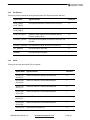
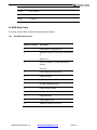
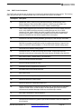
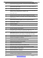
LVDS Flat Panel
These pins carry data for graphical display on an LVDS panel, as indicated.
4.1.9
Signal Name
Signal Function
Direction
LVDS_A[0:3]+
LVDS_A[0:3]-
LVDS Channel A differential pairs.
O
LVDS_A_CK+
LVDS_A_CK
LVDS Channel A differential clock.
O
LVDS_B[0:3]+
LVDS_B[0:3]-
LVDS Channel B differential pairs.
O
LVDS_B_CK+
LVDS_B_CK
LVDS Channel B differential clock.
O
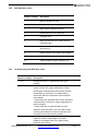
LVDS_VDD_EN
LVDS panel power enable.
O
LVDS_BKLT_EN
LVDS panel backlight enable.
O
LVDS_BKLT_CTRL
LVDS panel backlight brightness control.
O
LVDS_I2C_CK
I2C clock output for LVDS display use.
O
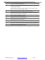
LVDS_I2C_DAT
I2C data line for LVDS display use.
I/O
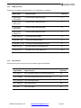
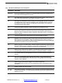
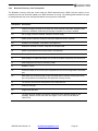
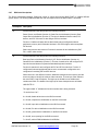
LPC Interface
These pins carry the Low Pin Count (LPC) interface signals, as indicated.
Signal Name
Signal Function
Direction
LPC_AD[0:3]
LPC multiplexed address, command and data bus.
I/O
LPC_FRAME#
LPC frame indicates the start of an LPC cycle.
O
LPC_DRQ[0:1]#
LPC serial DMA request.
I
LPC_SERIRQ
LPC serial interrupt.
I/O
LPC_CLK
LPC clock output.
O
CME-965 User Manual 1.0
www.diamondsystems.com
Page 21