1
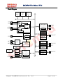
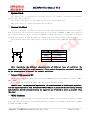
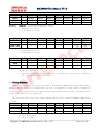
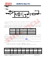
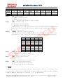
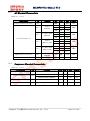
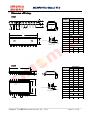
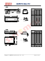
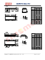
MC20P04 User Manual V1.2 8 Bit MCU designed by SinoMCU 2013/09/18 Note: Should there be any inconsistencies between Chinese and English version, the Chinese version shall prevail. 上海晟矽微电子股份有限公司 Shanghai SinoMCU Microelectronics Co., Ltd. SinoMCU reserves the right to make changes without further notice to any products herein. The information contained in this document may subsequently be updated or withdrawn, so the customer should ensure that it has the most up to date version. MC20P04 User Manual V1.2 Contents 1 Introduction ........................................................................ 4 1.1 Product characteristics ..................................................... 4 1.2 Block Diagram ............................................................... 5 1.3 Pin Assignment .............................................................. 6 1.4 Pin Description ............................................................. 7 1.5 Block Diagram of pins ....................................................... 8 2 CPU .............................................................................. 11 2.1 Instruction Set ............................................................ 11 2.2 Address Space .............................................................. 11 2.3 Program Memory ROM ......................................................... 11 2.4 Data Memory RAM ............................................................ 11 2.5 Configuration Bit – OPBIT.................................................. 11 2.6 Control Registers .......................................................... 12 3 System Clock ..................................................................... 13 3.1 External Oscillator ........................................................ 13 3.2 Internal High-accuracy RC .................................................. 13 3.3 WDT Oscillator ............................................................. 13 4 Reset ............................................................................ 14 4.1 Description ................................................................ 14 4.2 Power-on Reset ............................................................. 15 4.3 External rest .............................................................. 15 4.4 LVR Reset .................................................................. 15 4.5 WDT Reset .................................................................. 16 5 I/O .............................................................................. 17 5.1 IO Working Mode ............................................................ 17 5.2 Pull-up Resistor ........................................................... 18 5.3 Pull-down Resistor ......................................................... 19 6 Timer ............................................................................ 20 6.1 Timer ...................................................................... 20 6.2 WDT ........................................................................ 21 7 Comparator ....................................................................... 23 8 Interrupt ........................................................................ 25 8.1 General Description ........................................................ 25 8.2 External Interrupt ......................................................... 25 8.3 Keyboard Interrupt ......................................................... 26 8.4 TIMER Interrupt ............................................................ 27 8.5 WDT Interrupt .............................................................. 27 9 System working mode .............................................................. 28 9.1 STOP Mode .................................................................. 28 9.2 WAIT Mode .................................................................. 28 10 Electrical Specification ......................................................... 29 Shanghai SinoMCU Microelectronics Co., Ltd. Page 2 of 40 MC20P04 User Manual V1.2 10.1 Absolute Maximum Rating .................................................... 29 10.2 DC Electrical Characteristics............................................... 29 10.3 AC Electrical Characteristics............................................... 30 10.4 Comparator Electrical Characteristics....................................... 30 11 Dimension of Package ............................................................. 31 12 Appendix ......................................................................... 36 12.1 Characteristics Graph of Internal RC........................................ 36 12.2 Characteristics Graph of IO Port Driving Ability ............................ 37 12.3 Characteristics Graph of WAIT mode Operating Current ........................ 38 12.4 Characteristics Graph of Dynamic Supply Current ............................. 39 13 Revision History ................................................................. 40 Shanghai SinoMCU Microelectronics Co., Ltd. Page 3 of 40 MC20P04 User Manual V1.2 MC20P04 User Manual V1.2 1 Introduction MC20P04 is a high-performance, 8-bit Microcontroller. It has an internal high-accuracy RC oscillator circuit, two comparators. The high anti-interference performance of the product can provide good solutions for many kinds of small household appliances. 1.1 Product characteristics 8-bit CPU with CISC architecture 4K*8 bits OTP ROM 128 bytes RAM Three groups of IO port (17 GPIOs at most and one input port) Two comparators (offset can be adjusted by software) One 8-bit timer/counter, the clock source and trigger edge can be selected by software, overflow interrupt can be set 7 channels keyboard interrupt (KBI) 2 channels external interrupt (INT0/INT1),rising edge/failing edge/high level/low level trigger mode can be selected Watchdog Timer (WDT) with independent internal oscillator. Low voltage reset LVR(2.1V/3.6V selectable) 5 interrupt sources: INT0、INT1、TMI、KBI、WDTI Oscillator mode: Internal RC Oscillator : 2MHz、4MHz、8MHz selectable (accuracy <±1%,25℃,5V operating voltage) High frequency crystal oscillator: 400K-8MHz Low power consumption(<3mA@4MHz(5V),<1uA@STOP mode) Serial programming interface circuit Programmable Code Protection Operating voltage range 2.0-5.5V@ (400K-4MHz RC Frequency) 2.7-5.5V@ (400K-8MHz RC Frequency) Package: DIP20、SOP20、DIP18、SOP18、DIP16、SOP16、DIP14、SOP14、DIP8、SOP8 Shanghai SinoMCU Microelectronics Co., Ltd. Page 4 of 40 MC20P04 User Manual V1.2 1.2 Block Diagram 4K*8 OTP 128*8 RAM CP1P CP1N HC05 CPU + CMP1A CP0P CP0N CMPC + - EXT INT Controller INT0 INTC INT1 CMP0A P0 TCC OSCI Timer DDR0 TCR P0HCON TDR P0LCON P1 OSC OSCO Clock Generator Internal HRC Internal LRC WDT P00-P07 DDR1 P1HCON P10-P16 P17 KBIM LVR RESET Controller POR RSTFR P2 DDR2 P20-P21 RSTB Shanghai SinoMCU Microelectronics Co., Ltd. Page 5 of 40 MC20P04 User Manual V1.2 1.3 Pin Assignment P17/RSTB/VPP GND P00/INT0 5 6 7 P01/INT1 8 P02/CP0N 9 P03/CP0P 20 19 18 17 P12 P11 P10 P20/OSCI 16 15 14 P21/OSCO VDD P07/CP1P P06/CP1N 13 12 10 11 P12 P13 P16/TCC P17/RSTB/VPP 1 2 3 4 GND P00/INT0 P01/INT1 5 6 7 P05 P04 5 6 7 P03/CP0P 8 14 13 12 P02/CP0N 8 11 9 10 P04 DIP18/SOP18 16 15 14 13 P11 P10 P20/OSCI P21/OSCO 12 11 10 VDD P07/CP1P P06/CP1N P04 9 P11 P10 P20/OSCI P21/OSCO P03/CP0P P03/CP0P P06/CP1N P07/CP1P VDD 1 2 3 4 P21/OSCO P20/OSCI P11 5 6 7 MC20P04A0B/J GND P00/INT0 P02/CP0N MC20P04A0C/K 1 2 3 4 18 17 16 15 VDD P07/CP1P P06/CP1N P05 DIP20/SOP20 P12 P13 P16/TCC P17/RSTB/VPP MC20P04A0D/L 1 2 3 4 MC20P04A0E/M P13 P14 P15 P16/TCC 14 13 12 11 P02/CP0N P01/INT1 P00/INT0 GND 10 9 8 P17/RSTB/VPP P16/TCC P14 DIP14/SOP14 DIP16/SOP16 1 P17/RSTB/VPP GND P00/INT0 2 3 4 MC20P04A0A/H P16/TCC 8 P10 7 6 5 VDD P07/CP1P P06/CP1N DIP8/SOP8 Shanghai SinoMCU Microelectronics Co., Ltd. Page 6 of 40 MC20P04 User Manual V1.2 1.4 Pin Description NO. Pin direction Type - P13 I/O PU GPIO, pull-up resistor selectable, KBI function 8 - P14 I/O PU GPIO, pull-up resistor selectable, KBI function - - - P15 I/O PU GPIO, pull-up resistor selectable, KBI function 3 9 1 I/O PU 20pin 18pin 16pin 14pin 8pin 1 2 2 - 2 - - 3 - 4 3 P16 TCC P17 5 4 4 10 2 RSTB 5 5 11 3 7 6 6 12 4 8 7 - 13 - 9 8 7 14 - 10 9 8 1 - 11 10 9 - - 12 11 - - - 13 12 10 2 5 14 13 11 3 6 15 14 12 4 7 16 15 13 5 - 17 16 14 6 - 18 17 15 - 8 19 18 16 7 20 1 1 - GND P00 GPIO, pull-up resistor selectable, KBI function TCC input Input port, pull-up resister selectable I PI VPP 6 Functional Description External reset input Programming high voltage input P Ground GPIO, pull-up/pull-down resistor selectable I/O PUD I/O PUD I/O PUDC I/O PUDC P04 I/O PUD GPIO, pull-up/pull-down resistor selectable P05 I/O PUD GPIO, pull-up/pull-down resistor selectable I/O PUDC I/O PUDC INT0 P01 INT1 P02 CP0N P03 CP0P P06 CP1N P07 CP1P VDD P21 P External interrupt 0 input GPIO, pull-up/pull-down resistor selectable External interrupt 1 input GPIO, pull-up/pull-down resistor selectable Comparator 0 negative input GPIO, pull-up/pull-down selectable Comparator 0 positive input GPIO, pull-up/pull-down resistor selectable Comparator 1 negative input GPIO, pull-up/pull-down resistor selectable Comparator 0 positive input Power Supply GPIO I/O PIO I/O PIO P10 I/O PU GPIO, pull-up resistor selectable, KBI function - P11 I/O PU GPIO, pull-up resistor selectable, KBI function - P12 I/O PU GPIO, pull-up resistor selectable, KBI function OSCO P20 OSCI Shanghai SinoMCU Microelectronics Co., Ltd. Crystal Oscillator GPIO Crystal Oscillator Page 7 of 40 MC20P04 User Manual V1.2 1.5 Block Diagram of pins PI OPTION.6 Programming High Voltage Pin OPTION.3 Reset ` Data Bus RD PU Pull-up Enable Output Enable Pin Data Bus WR D Q CLX QB MUX RD Shanghai SinoMCU Microelectronics Co., Ltd. Page 8 of 40 MC20P04 User Manual V1.2 PUD Pull-up Enable Output Enable Pin Data Bus WR D Q CLK QB MUX RD Pull-down Enable PUDC Pull-up Enable Output Enable Comp Enable To Comparator Pin Data Bus WR D Q CLK QB MUX RD Pull-down Enable Shanghai SinoMCU Microelectronics Co., Ltd. Page 9 of 40 MC20P04 User Manual V1.2 PIO OSC Enable Output Enable Pin Data Bus WR D Q CLK QB MUX To OSC Circuit RD Shanghai SinoMCU Microelectronics Co., Ltd. Page 10 of 40 MC20P04 User Manual V1.2 2 CPU 2.1 Instruction Set MC20P04 uses HC05 compatible instruction set. For detail information about instruction set, please refer to the “HC05 instruction Set” provided by SinoMCU. Note: MC20P04 does not support MUL instruct. 2.2 Address Space $0000-$0011:Control Register $0012-$007F:Reserved $0080-$00FF:RAM(share by Stack) $0100-$0FFF:Reserved $1000-$1FFF:OTP ROM 2.3 Program Memory ROM Program memory of MC20P04, which is an OTP ROM with size of 4K bytes (8 bit) to store instructions. The address ($1FE0~$1FFF) of program memory is reset/interrupt vector area , Refer to (§8.1). 2.4 Data Memory RAM Data memory of MC20P04 has 128 bytes (8 bits), which are shared with stack. For more information about stack, please refer to the datasheet “HC05 Instruction Set”. 2.5 Configuration Bit – OPBIT Configuration Bit (OPBIT) is a special bit in OTP. It is used as configuring system functions. OPBIT can be programmed by SinoMCU programmer. The OPBIT of MC20P04 is defined as follows. BIT[7] BIT[6] BIT[5] BIT[4] Bit 7 Bit 6 Bit 5 Bit 4 Bit 3 Bit 2 Bit 1 Bit 0 OPBIT ENCR RESE LVRE LVRS RSTE WDTE0 OSCS1 OSCS0 ENCR - Program memory protection bit 0:Protection is enabled 1:Protection is disabled RESE – P17/RSTB pull-up resistor selection 0:Pull-up resistor is disabled 1:Pull-up resistor is enabled LVRE – LVR enabled 0:LVR turn on 1:LVR turn off LVRS – LVR voltage selection 0:LVR voltage 2.1V Shanghai SinoMCU Microelectronics Co., Ltd. Page 11 of 40 MC20P04 User Manual V1.2 BIT[3] BIT[2] BIT[1:0] 1:LVR voltage 3.6V RSTE – P12/RSTB function selection 0:P17/RSTB pin as input port 1:P17/RSTB pin as external reset port WDTE0 – WDT enable 0:WDT enable(WDTE bit in MCR register should be set to 1) 1:WDT disable OSCS[1:0] – System clock selection 00:Internal RC oscillator 2MHz 01:External 400K~8MHz crystal oscillator 10:Internal RC oscillator 4MHz 11:Internal RC oscillator 8MHz 2.6 Control Registers All the registers of MC20P04 are listed below. Detail functions of these registers are described in the following contents. Address Name R/W Bit 7 Bit 6 Bit 5 Bit 4 $00 P0 R/W P07 P06 P05 P04 P03 P02 $01 DDR0 R/W DDR07 DDR06 DDR05 DDR04 DDR03 DDR02 $02 P0HCON R/W PH07 PH06 PH05 PH04 PH03 PH02 $03 P0LCON R/W PL07 PL06 PL05 PL04 PL03 $04 P1 R/W P17 P16 P15 P14 P13 $05 DDR1 R/W - DDR06 DDR15 DDR14 DDR13 $06 P1HCON R/W - PH16 PH15 PH14 PH13 PH12 $07 KBIM R/W - KBIM6 KBIM5 KBIM4 KBIM3 KBIM2 $08 P2 R/W - - - - - - $09 DDR2 R/W - - - - - $0A TDR R/W TDR7 TDR6 TDR5 TDR4 $0B TCR R/W TIF TIM PR2 PR1 $0C INTC R/W INT0E INT0M1 INT0M0 INT0F $0D MCR R/W KBIE KBIC WDTE WDTC WDTF WDTM $0E RSTFR R/W - - - - WDTRF LVRRF $0F CMPC R/W - - - - C1VO C1EN $10 CMP0A R/W C0OFM C0CRS C0OF5 C0OF4 C0OF3 $11 CMP1A R/W C1OFM C1CRS C1OF5 C1OF4 C1OF3 Shanghai SinoMCU Microelectronics Co., Ltd. Bit 3 Bit 2 Bit 1 Bit 0 Initial value P01 P00 0000 0000 DDR01 DDR00 0000 0000 PH01 PH00 0000 0000 PL02 PL01 PL00 0000 0000 P12 P11 P10 X000 0000 DDR12 DDR11 DDR10 -000 0000 PH11 PH10 -000 0000 KBIM1 KBIM0 -000 0000 P21 P20 ---- --00 - DDR21 DDR20 ---- --00 TDR3 TDR2 TDR1 TDR0 XXXX XXXX PR0 PTA PTS PTE 0101 1000 INT1E INT1M1 INT1M0 INT1F 0000 0000 USEL - 0000 000- RSTRF PORRF ---- 0000 C0VO C0EN ---- 0000 C0OF2 C0OF1 C0OF0 0010 0000 C1OF2 C1OF1 C1OF0 0010 0000 Page 12 of 40 MC20P04 User Manual V1.2 3 System Clock The signal Fosc is generated by external crystal (or ceramic) oscillator or internal high-accuracy RC oscillator. The system clock (Fsys) is 1/2 frequency division of the signal Fosc. WDT clock source is internal frequency RC oscillator. 3.1 External Oscillator Crystal (or ceramic) oscillator is connected as following diagram when the external oscillator mode is selected. The oscillator frequency must be in the range of 400KHz to 8MHz. The capacitor Cx is usually required. It is strongly recommended to make the crystal (or ceramic) oscillator as short as possible to OSCI and OSCO pin, because of oscillating starting and stability. The following table lists some typical oscillator frequency and recommended capacitance value of Cx. Cx Cx Osc. Freq. Capacitance of Cx 8MHz 15p 4MHz 15p/30p 3.64MHz 15p/30p 455KHz 100p-300p Note: Considering the different characteristics of different types of oscillator, the capacitance value listed are merely suggested. Please select the capacitor cautiously according to the characteristic of crystal (or ceramic) oscillator. 3.2 Internal High-accuracy RC The internal high-performance RC oscillator of MC20P04 has three frequency to select: 2MHz, 4MHz, 8MHz. While selecting internal RC mode, P20 and P21 can be used as GPIO. Special note: In the practical application, it needs to connect an electrolytic capacitor, with the capacitance above 10uF, between the VDD and GND pin to guarantee the oscillating accuracy and stability. And the distance between the capacitor and IC should as short as possible (less than 5cm). 3.3 WDT Oscillator MC20P04 has a low frequency oscillator (frequency 64KHz), The oscillator is used by the WDT only, and cannot be used as a system clock. Whether oscillator is enabled is determined by WDTE0 in OPBIT and WDTE in MCR. Shanghai SinoMCU Microelectronics Co., Ltd. Page 13 of 40 MC20P04 User Manual V1.2 4 Reset 4.1 Description MC20P04 has four mode of reset: Power-on reset POR External reset Low Voltage reset LVR WDT reset The system will fetch reset vector address from address $1FFE:$1FFF while any kinds of reset occurs, all the registers will be set to initial value. The system clock oscillator will be disabled by POR or LVR, oscillator will be enabled after reset released. Because the oscillator need enough time to establishing and stability, the system will work after 4096 clocks delay. External reset and WDT reset will not shut the system clock oscillator, when reset is released, it will start working after 2 clock cycle. Below diagram describes the reset procedure. POR Detect Voltage LVR Detect Voltage VDD POR/LVR Reset GND VDD External Reset GND External Rest Detect Voltage WDT Overflow WDT Overflow WDT Reset WDT Count Normal Working System State Stop Working While reset occurs, the corresponding flag bit in RSTFR will be set. Bit 7 Bit 6 Bit 5 Bit 4 Bit 3 $10 WDTRF RSTFR R/W R/W 0 Initial value BIT[3] WDTRF – WDT reset flag 0:No WDT reset occurred 1: WDT reset occurred Write‘0’to clear flag; write‘1’invalid BIT[2] LVRRF –LVR reset flag Shanghai SinoMCU Microelectronics Co., Ltd. Bit 2 LVRRF R/W 0 Bit 1 RSTRF R/W 0 Bit 0 PORRF R/W 0 Page 14 of 40 MC20P04 User Manual V1.2 BIT[1] BIT[0] 0: No LVR reset occurred 1: LVR reset occurred Write‘0’to clear flag; write‘1’invalid RSTRF –External Port reset flag 0:No External Port reset occurred 1: External Port reset occurred Write‘0’to clear flag; write‘1’invalid PORRF –power-on reset flag 0:No Power-on reset occurred 1: Power-on reset occurred Write‘0’to clear flag; write‘1’invalid 4.2 Power-on Reset Power-on reset circuit of MC20P04 can adapt to the fast or slow supply voltage rising, and make the system reset when supply voltage jitter occurs. The steps of Power-on reset as follow: (1) Waiting for voltage higher than VPOR and keep stability; (2) Waiting for the reset pin voltage higher than VIH when the external port reset functions is enabled. (3) Reset PC pointer and initialize all registers; (4) System clock oscillator start, and waits for 4096 clock period; (5) System executes instruction. 4.3 External rest Whether the external reset is enabled can be configured by the RSTE in the OPBIT. And RESE can select to enable the internal pull-up resistor of the pin.(refer to§2.5).The external reset pin is Schmidt structure, low level effective. 4.4 LVR Reset ① The LVR voltage of MC20P04 has two levels: (2.1V 和 3.6V ), LVR function is configured by VBORS in OPBIT (refer to §2.5).The low voltage detection circuit has hysteretic characteristics; usually the hysteretic voltage is about 0.05V. In this case, if 3.6V voltage selectable, LVR reset action while the supply voltage low to 3.6V, and the reset is released while the voltage up to 3.65V. Note①:LVR voltage 2.1V and 3.6V used as design reference only, error obviously, cannot be used as accurate voltage detection. Note②:0.05V is theoretical value. Shanghai SinoMCU Microelectronics Co., Ltd. Page 15 of 40 MC20P04 User Manual V1.2 4.5 WDT Reset WDT reset is the protection mechanism for normal operation of the system. Usually, user will clear the WDT timer to zero regularly; the timer will not be overflow. If the system is out of the conditions exceptionally, WDT timer will be overflow and reset system, then the system initial and return to controlled state. WDT has an independent internal RC oscillator, WDT reset will be occurs when the system clock oscillator is stopped , the time range of WDT overflow is 32ms~4096ms with different division. About the WDT watchdog timer details, (refer to §6.2). Shanghai SinoMCU Microelectronics Co., Ltd. Page 16 of 40 MC20P04 User Manual V1.2 5 I/O 5.1 IO Working Mode MC20P04 has 17 general bi-directional IO port (P07-P00、P16-P10、P21-P20)and input port(P17). Each bi-directional IO port is controlled by the corresponding Data Register (P0, P1, P2) and direction register (DDR0, DDR1, DDR2). The function of data register and direction register is listed below. R/W DDR Function W 0 IO port is input port. Data is written to the output data register. W 1 IO port is output port. Data is written to the output register and output to the port R 0 IO port is input port. Data is read from ports R 1 IO port is Output port. Data is read from the output data register When system is configured to the external crystal oscillator mode, P20 and P21 cannot be used as IO port, the corresponding register control bit is invalid. The master clock is output at P21 when USEL=1 in MCR and P21 set as output port. Bit 7 Bit 6 Bit 5 Bit 4 $00 P07 P06 P05 P04 P0 R/W R/W R/W R/W R/W 0 0 0 0 Initial Value BIT[7:0] P0n – P0 Data register(n=7-0) Bit 3 P03 R/W 0 Bit 2 P02 R/W 0 Bit 1 P01 R/W 0 Bit 0 P00 R/W 0 Bit 7 $04 P17 P1 R R/W X Initial Value BIT[7:0] P1n – P1 Bit 6 Bit 5 Bit 4 P16 P15 P14 R/W R/W R/W 0 0 0 Data register(n=7-0) Bit 3 P13 R/W 0 Bit 2 P12 R 0 Bit 1 P11 R/W 0 Bit 0 P10 R/W 0 Bit 7 Bit 6 Bit 5 Bit 4 $08 P2 R/W Initial Value BIT[1:0] P2n – P2 Data register(n=1-0) Bit 3 - Bit 2 - Bit 1 P21 R/W 0 Bit 0 P20 R/W 0 $01 DDR0 R/W Initial Value BIT[7:0] Bit 7 DDR07 R/W Bit 6 DDR06 R/W Bit 5 DDR05 R/W Bit 4 DDR04 R/W Bit 3 DDR03 R/W Bit 2 DDR02 R/W Bit 1 DDR01 R/W Bit 0 DDR00 R/W 0 0 0 0 0 0 0 0 DDR0n – P0 Direction Register(n=7-0) 0:Configured to input Shanghai SinoMCU Microelectronics Co., Ltd. Page 17 of 40 MC20P04 User Manual V1.2 1:Configured to output Bit 7 Bit 6 Bit 5 Bit 4 Bit 3 $05 DDR16 DDR15 DDR14 DDR13 DDR1 R/W R/W R/W R/W R/W 0 0 0 0 Initial Value BIT[6:0] DDR1n –P1 Direction Register(n=6-0) 0:Configured to input 1:Configured to output Bit 7 Bit 6 Bit 5 Bit 4 $09 DDR2 R/W Initial Value BIT[1:0] DDR2n –P2 Direction Register(n=1-0) 0:Configured to input 1:Configured to output Bit 3 - Bit 2 DDR12 R/W 0 Bit 1 DDR11 R/W 0 Bit 0 DDR10 R/W 0 Bit 2 - Bit 1 DDR21 R/W 0 Bit 0 DDR20 R/W 0 Bit 7 Bit 6 Bit 5 Bit 4 Bit 3 Bit 2 Bit 1 Bit 0 $0D KBIE KBIC WDTE WDTC WDTF WDTM USEL MCR R/W R/W R/W R/W R/W R/W R/W R/W 0 0 0 0 0 0 0 Initial Value BIT[1] USEL – System clock output enable bit 0:P21 is a GPIO port 1:System clock(Fosc) output at P21(P21 is configured to output port, and work in the internal RC oscillation mode) 5.2 Pull-up Resistor Whether P0 and P1 pull-up resistor enabled is determined by PDCON and PUCON(approximately 25KΩ). Pull-up resistor is enabled when the port is configured to input state. Configured to output port is not affected even though pull-up resistor enabled. The pull-up/pull-down resistor of P0 can be enabled at the same time. The pull-up resistor of P17 port (approximately 50 KΩ) can be enabled by RESE in OPBIT (refer to§2.5). Bit 7 Bit 6 Bit 5 Bit 4 Bit 3 $02 PH07 PH06 PH05 PH04 PH03 P0HCON R/W R/W R/W R/W R/W R/W 0 0 0 0 0 Initial Value BIT[7:0] PH0n – P0 port pull-up selection(n=7-0) 0:Pull-up disable 1:Pull-up enable Shanghai SinoMCU Microelectronics Co., Ltd. Bit 2 PH02 R/W 0 Bit 1 PH01 R/W 0 Bit 0 PH00 R/W 0 Page 18 of 40 MC20P04 User Manual V1.2 Bit 7 Bit 6 Bit 5 Bit 4 Bit 3 $05 PH16 PH15 PH14 PH13 P1HCON R/W R/W R/W R/W R/W 0 0 0 0 Initial Value BIT[6:0] PH1n – P1 port pull-up selection(n=6-0) 0:Pull-up disable 1:Pull-up enable Bit 2 PH12 R/W 0 Bit 1 PH11 R/W 0 Bit 0 PH10 R/W 0 5.3 Pull-down Resistor Whether P0 pull-down resistor enabled is determined by PDCON and PUCON(approximately 25K Ω). Pull-down resistor is enabled when the port is configured to input state. Configured to output port is not affected even though pull-up resistor enabled. The pull-up/pull-down resistor of P0 can be enabled at the same time. Bit 7 Bit 6 Bit 5 Bit 4 Bit 3 $03 PL07 PL06 PL05 PL04 PL03 P0LCON R/W R/W R/W R/W R/W R/W 0 0 0 0 0 Initial Value BIT[7:0] PL0n –P1 port pull-down selection(n=7-0) 0:Pull-down disable 1:Pull-down enable Shanghai SinoMCU Microelectronics Co., Ltd. Bit 2 PL02 R/W 0 Bit 1 PL01 R/W 0 Bit 0 PL00 R/W 0 Page 19 of 40 MC20P04 User Manual V1.2 6 Timer 6.1 Timer ÷2 Fsys TIM 0 Fosc 1 1 PTE TCK 1 ÷2 0 Prescaler 0 1 PTS MUX ÷1 ÷2 ÷4 ÷8 ÷16 ÷32 ÷64 ÷128 0 TCC TDR Count-down Counter TOV T0IF TMI interrupt request PTA WDTCK 0 PR[2:0] 1 PTA Fwdt PTA The timer of MC20P04 contains an 8-bit programmable count-down counter and 7-bit programmable prescaler. The clock source of TDR comes from system clock Fsys(Fosc/2)or other division set by PR or external pin signal (rising-edge/failling edge is selectable). The prescaler of timer is shared with WDT;when PTA=0, The prescaler is assigned to T0; when PTA=1,prescaler is assigned to WDT. Prescaler division is controlled by PR [2:0]. TCK WDTCK (multiple of Fsys) (multiple of Fwdt) n 2n+1 1 n 1 2n PTA PR[2:0] 0 1 The counter preset value can be set and decrements towards zero with clock. When the counter decrements to zero, the timer interrupt flag (TIF bit in TCR) is set. Once the interrupt flag is set, an interrupt is generated to CPU when TIM bit in TCR is set and I-bit in CCR is cleared. For more information about interrupt, please refer to §8.4. The counter (TDR) may be read at any time without disturbing the counting. If writing a new value to TDR, the counter will count from the new value immediately. The prescaler cannot writable and readable; however, it can be cleared by two conditions as below. (1)PTA=0,The prescaler is assigned to TIMER,TDR is written. (2)PTA=1,The prescaler is assigned to WDT, WDTC in MCR register is cleared. Here are the relative registers of TIMER. $0A TDR R/W Initial Value Bit 7 TDR 7 R/W X Bit 6 Bit 5 Bit 4 Bit 3 Bit 2 Bit 1 Bit 0 TDR6 TDR5 TDR4 TDR3 TDR2 TDR1 TDR0 R/W X R/W X R/W X R/W X R/W X R/W X R/W X Shanghai SinoMCU Microelectronics Co., Ltd. Page 20 of 40 MC20P04 User Manual V1.2 BIT[7:0] TDR[7:0] –TDR is a read/write register which contains the current value of TDR. Bit 7 Bit 6 Bit 5 Bit 4 Bit 3 Bit 2 Bit 1 Bit 0 TIF TIM PR2 PR1 PR0 PTA PTS PTE R/W R/W R/W R/W R/W R/W R/W R/W 初始值 0 1 0 1 1 0 0 0 BIT[7] TIF –Overflow flag 0:TIMER overflows un-occur 1:TIMER overflows occur Write ‘0’clears TIF. Write‘1’ has no effect. BIT[6] TIM –interrupt mask 0:TMI Timer interrupt enable 1:TMI Timer interrupt disable TIM will be set to ‘1’ when system reset, in this case, TMI interrupt will be disabled. TIM must be cleared to enable TMI interrupt. TIM is used to disabled interrupt request, but TIF is still valid. BIT[5:3] PR[2:0] –prescaler division selection The prescaler is shared by TIMER and WDT,it will be set to 011 when system reset. The table list below is the value of PR [2:0] and the corresponding division ratio. $0B TCR R/W BIT[2] BIT[1] BIT[0] PR0[2] PR0[1] PR0[0] TIMER WDT 0 0 0 2 1 0 0 1 4 2 0 1 0 8 4 0 1 1 16 8 1 0 0 32 16 1 0 1 64 32 1 1 0 128 64 1 1 1 256 128 PTA –Frequency assign 0:Frequency is assigned to TIMER 1:Frequency is assigned to WDT PTS –Clock source selection 0: System clock 1: TCC pin signal(P16 set to input port) PTE – TCC signal edge selection 0:Counting with TCC pin rising-edge 1:Counting with TCC pin failling-edge 6.2 WDT WDT is driving by the internal RC oscillator (please refer to §3.3),it can select if go by the prescaler. (Please refer to §6.1). WDT can generate WDT reset or WDTI interrupt. The WDTE in MCR and WDTEO in OPBIT must be configured to‘1’for WDT working. Shanghai SinoMCU Microelectronics Co., Ltd. Page 21 of 40 MC20P04 User Manual V1.2 WDT overflow will cause WDT reset when WDTM cleared. WDT overflow will cause WDTI interrupt when WDTM set. The clock source of WDT is independent of the system clock. So the WDT will still run even if the system is in STOP mode And WDT reset or WDTI interrupt can still work normally. WDT is an 11 bits counter. When counter is overflow, system will be reset, WDTF bit will be set, WDTI interrupt request will occurs. WDTC is used for clear WDT, WDT will be cleared when WDTC write ‘1’. The value of WDT cannot writable or readable. 11 18 The nominal time-out period of the WDT timer is 2 /Fwdt~2 /Fwdt with the frequency division ratio. The Fwdt frequency value is 64KHz,so the nominal time-out period of WDT is 32ms~4096ms. Here are the relative registers of WDT timer. Bit 7 Bit 6 Bit 5 Bit 4 Bit 3 Bit 2 Bit 1 Bit 0 $0D KBIE KBIC WDTE WDTC WDTF WDTM USEL MCR R/W R/W R/W R/W R/W R/W R/W R/W 0 0 0 0 0 0 0 Initial Value BIT[5] WDTE – WDT timer enable bit 0:WDT disable 1:WDT enable(WDTE0 in OPBIT must be configured to 1) BIT[4] WDTC – WDT timer clear bit WDTC always reads as zero. Write‘1’, the WDT is cleared; write‘0’is invalid. BIT[3] WDTF – WDT TIMER overflow flag 0:WDT overflag un-occurred 1:WDT overflow occurred Write‘0’, the flag is cleared, write‘1’is invalid. BIT[2] WDTM – WDT TIMER working mode selection 0:WDT overflow will cause system reset 1:WDT overflow will cause WDTI interrupt Shanghai SinoMCU Microelectronics Co., Ltd. Page 22 of 40 MC20P04 User Manual V1.2 7 Comparator MC20P04 includes two comparators: COMP and COMP1. When C0EN=1, the function of COMP0 is turn on. The positive input and negative input of comparators joined to P02 and P03 (the GPIO function of the two pins will be disabled automatically), the output of the comparator can be read by bit C0VO. Similarly, when C1EN=1, the function of COMP1 is turn on. The positive input and negative input of comparators joined to P06 and P07 (the GPIO function of the two pins will be disabled automatically), the output of the comparator can be read by bit C1VO. The input offset is adjustable. The calibration steps as following: CPnN S1 S2 CPnP S3 CnVO + (1)Set CnOFM to enter offset calibrate mode (S3 is closed) (2)Setting CnCRS to select offset calibrate port(S1 or S2 is closed) (3)Change CnOF[5:0] until output CnVO status is changed; (4)Clear CnOFM=0 to exit offset calibrate mode Here are the relative registers. Bit 7 Bit 6 Bit 5 Bit 4 Bit 3 Bit 2 Bit 1 Bit 0 $0F C1VO C1EN C0VO C0EN CMPC R R/W R R/W R/W 0 0 0 0 Initial Value BIT[3] C1VO –Comparator COMP1 output(positive logic) ,read-only bit BIT[2] C1EN –Comparator COMP1 enable bit 0:COMP1 disable 1:COMP1 enable(the GPIO function of P06 and P07 is disabled automatically) BIT[1] C0VO –Comparator COMP0 output(positive logic) ,read-only bit BIT[0] C0EN –Comparator COMP1 enable bit 0:COMP0 disable 1:COMP0 enable(the GPIO function of P02 and P03 is disabled automatically) Bit 7 Bit 6 Bit 5 Bit 4 Bit 3 $10 C0OFM C0CRS C0OF5 C0OF4 C0OF3 CMP0A R/W R/W R/W R/W R/W R/W 0 0 1 0 0 Initial Value BIT[7] C0OFM –Comparator COMP0 mode 0:Comparator mode 1:Input offset calibrate mode BIT[6] C0CRS –Comparator COMP0 offset calibrate port 0:CP0N selection Shanghai SinoMCU Microelectronics Co., Ltd. Bit 2 C0OF2 R/W 0 Bit 1 C0OF1 R/W 0 Bit 0 C0OF0 R/W 0 Page 23 of 40 MC20P04 User Manual V1.2 BIT[5:0] 1:CP1N selection C0OF[5:0] –Comparator COMP0 calibrate data Bit 7 Bit 6 Bit 5 Bit 4 Bit 3 $11 C1OFM C1CRS C1OF5 C1OF4 C1OF3 CMP1A R/W R/W R/W R/W R/W R/W 0 0 1 0 0 Initial Value BIT[7] C1OFM –Comparator COMP1 mode 0:Comparator mode 1:Input offset calibrate mode BIT[6] C1CRS –Comparator COMP1 offset calibrate port 0:CP0N selection 1:CP1N selection BIT[5:0] C1OF[5:0] –Comparator COMP1 calibrate data Shanghai SinoMCU Microelectronics Co., Ltd. Bit 2 C1OF2 R/W 0 Bit 1 C1OF1 R/W 0 Bit 0 C1OF0 R/W 0 Page 24 of 40 MC20P04 User Manual V1.2 8 Interrupt 8.1 General Description The interrupts of MC20P04 are external interrupt(INT0,INT1),keyboard interrupt (KBI), timer interrupt (TMI),WDT overflow interrupt(WDTI)and software interrupt (SWI). INT0, INT1, KBI, TMI and WDTI can be masked by I bit, which is in CPU status control register CCR, but SWI cannot be masked. Furthermore, SWI is also an instruction. For details about SWI, please refer to the data sheet ‘HC05 Instruction Set’. The process of interrupt service is: While interrupt request occurring, CPU pushes all the relative registers (5 bytes altogether) to stack, set I bit to ‘1’, and mask all the other interrupts. Differently from system reset, hardware interrupt does not terminate current instruction execution, but suspends itself until current instruction finished. While responding interrupt, firstly, CPU fetches the address of the interrupt service subroutine from the corresponding interrupt vector, then jumps to the subroutine and executes. Each interrupts service subroutine needs an RTI instruction. When executing RTI, CPU pops all the relative registers from stack, and executes the instruction exactly after the interrupt happened. The interrupt vectors are shown below. The priority is decreased from bottom to top in the list. INT Vector Address Interrupt $1FE0~$1FF1 Reserved $1FF2:$1FF3 WDTI $1FF4:$1FF5 KBI $1FF6:$1FF7 TMI $1FF8:$1FF9 INT1 $1FFA:$1FFB INT0 $1FFC:$1FFD SWI $1FFE:$1FFF RESET 8.2 External Interrupt P00 and P01 of MC20P04 can be used as external interrupt input INT0 and INT1, four kinds of interrupt conditions can be responded, which is rising edge, falling edge, high level, and low level. The function of external interrupt INT0 control bit as below: (1)INT0E is the interrupt enable bit, when INT0E=0,external interrupt disable;when INT0E=1, external interrupt enable. ( 2 ) INT0M[1:0]is the interrupt trigger mode bit , which contains falling-edge trigger, rising-edge trigger,high level trigger,low level trigger. Shanghai SinoMCU Microelectronics Co., Ltd. Page 25 of 40 MC20P04 User Manual V1.2 (3)INT0F is the interrupt flag bit,INT0F could not be cleared automatically,must be cleared by software. When INT0E=0, INT0F is not affected when port changing. The function of external INT1 control bit the same as external INT0. Note: If using the external interrupt INT0, the P00 port must be set to input state with DDR00=0. If using the external interrupt INT1, the P01 port must be set to input state with DDR01=0. Here are the relative registers: Bit 7 Bit 6 Bit 5 Bit 4 Bit 3 $0B INT0E INT0M1 INT0M0 INT0F INT1E INTC R/W R/W R/W R/W R/W R/W 0 0 0 0 0 Initial Value BIT[7] INT0E – INT0 enable bit 0:INT0 disable 1:INT0 enable BIT[6:5] INT0M[1:0] – INT0 trigger selection 00:Falling-edge trigger 01:Rising-edge trigger 10:Low-level trigger 11:High-level trigger BIT[4] INT0F – INT0 flag bit 0:INT0 interrupt un-occur 1:INT0 interrupt occur Write ‘0’to clear flag, write ‘1’is invalid. BIT[3] INT1E – INT1 enable bit 0:INT1 disable 1:INT1 enable BIT[2:1] INT1M[1:0] – INT1 trigger selection 00:Falling-edge trigger 01:Rising-edge trigger 10:Low-level trigger 11:High-level trigger BIT[0] INT1F – INT1 flag bit 0:INT1 interrupt un-occur 1:INT1 interrupt occur Write ‘0’ to clear flag, write ‘1’ is invalid. Bit 2 INT1M1 R/W 0 Bit 1 INT1M0 R/W 0 Bit 0 INT1F R/W 0 8.3 Keyboard Interrupt P16-P10 of MC20P04 can be used as keyboard interrupt inputs. All the keyboard interrupt inputs shared same interrupt vector. To determine which port triggers the interrupt by read from GPIO’s data register. The function of keyboard interrupt control bit as below: (1)KBIE is enable bit of KBI,while KBIE=1,KBI interrupt enable. While KBIE=0,KBI interrupt disable. Shanghai SinoMCU Microelectronics Co., Ltd. Page 26 of 40 MC20P04 User Manual V1.2 (2)KBIM[6:0] (corresponding to P1[6:0]) are mask bit of KBI,while KBIMn=1,which means the KBI interrupt function of P1n is enable. Otherwise, KBI function is disabling. (3)When the input level of P16-P10 is from high-level to low-level , the keyboard interrupt request will be triggered. Besides, the control bit KBIC in MCR is used to clear keyboard interrupt request. While the keyboard interrupt request is responded, write‘1’ to KBIC. Otherwise, keyboard interrupt request will be latched. That means if KBIC not write‘1’, keyboard interrupt will be requested continuity. Here are the relative registers: $0D MCR R/W 初始值 BIT[7] BIT[6] $07 KBIM R/W 初始值 BIT[6:0] Bit 7 Bit 6 Bit 5 Bit 4 Bit 3 KBIE KBIC WDTE WDTC WDTF R/W R/W R/W R/W R/W 0 0 0 0 0 KBIE –keyboard interrupt enable bit 0:Keyboard interrupt disable 1:Keyboard interrupt enable KBIC –keyboard interrupt signal latch 0:Undefined 1:Keyboard interrupt latch signal is cleared KBIC always reads as zero. Bit 2 WDTM R/W 0 Bit 1 USEL R/W 0 Bit 0 - Bit 7 Bit 6 Bit 5 Bit 4 Bit 3 Bit 2 Bit 1 Bit 0 KBIM6 KBIM5 KBIM4 KBIM3 KBIM2 KBIM1 KBIM0 R/W R/W R/W R/W R/W R/W R/W 0 0 0 0 0 0 0 KBIM0n – P1n port keyboard interrupt mask bit(n=6-0) 0:Mask keyboard interrupt 1:Un-mask Keyboard interrupt P1n port set to input state Automatically) 8.4 TIMER Interrupt The TIMER overflow will cause interrupt request TMI, which controlled by mask bit and flag bit. Please refer to§6.1. 8.5 WDT Interrupt While WDTM=1,WDT overflow will cause interrupt request WDTI. Please refer to §6.2. Shanghai SinoMCU Microelectronics Co., Ltd. Page 27 of 40 MC20P04 User Manual V1.2 9 System working mode MC20P04 has two kinds of Low power consumption mode: STOP mode and WAIT mode. 9.1 STOP Mode The instruction STOP makes system enter STOP mode, which has several effects bellow: System oscillator stops Clear I bit in CCR, and enable interrupt request RAM data hold All states of GPIO remain All the internal operation stops If any condition is happened as below, system will exit from STOP mode. External interrupt INT0,INT1 request occurs KBI request occurs Timer overflow interrupt TMI( when timer clock source is pin TCC) request occurs WDT overflow cause WDTI interrupt request occurs Any type of system reset occurs While system works in STOP mode, almost all the operations stop, so the power consumption is very low. 9.2 WAIT Mode The instruction WAIT makes system enter WAIT mode, which has several effects bellow: CPU clock stops CPU and internal bus activities terminate TIMER keep working Clear I bit in CCR, and enable interrupt request RAM data hold All states of GPIO remain All states of registers remain If one of the following things happens, CPU clock will restarts and system will exit WAIT mode. Any type of interrupt request occur Any type of system reset occurs While system works in WAIT mode, CPU stop, but the system oscillator still works, so the power consumption is lower than normal mode. Shanghai SinoMCU Microelectronics Co., Ltd. Page 28 of 40 MC20P04 User Manual V1.2 10 Electrical Specification 10.1 10.2 Absolute Maximum Rating Parameter Symbol Ratings/Value Unit Operating Voltage VDD -0.3~6.5 V Input Voltage VIN VSS-0.3~ VDD+0.3 V Operating Temperature TA -40~85 ℃ Storage Temperature Tstg -65~150 ℃ DC Electrical Characteristics (VDD=5V,T=25℃) Characteristics Symbol Pin Operating Voltage VDD Input Leakage Current Vleak All input ports Input High Level Vih All input ports Input Low Level Vil All input ports Pull-up Resistor 1 RU1 Pull-up Resistor 2 RU2 Pull-down Resistor Condition Min. 400K-4M 400K-8M Typ. Max. Unit 2.0 5.5 V 2.7 5.5 V ±1 uA 0.7VDD VDD V 0 0.3VDD V VIN=VDD,0 P00-P07 10 25 50 Kohm P17 20 50 100 Kohm RD P00-P07 10 25 Output High Level Drive Current Ioh All input ports Voh=VDD-0.7V 6 Output Low Level Drive Current Iol All input ports Vol=0.7V 10 Power-down current Power supply current Idds Iddc P10-P16 VDD VDD Close LVR, Close WDT Open WDT Open LVR VDD=5V Kohm 50 mA mA 0.5 1 uA 10 0.5 15 1 uA 3 mA Fosc=4MHz no load LVR Vlvr Shanghai SinoMCU Microelectronics Co., Ltd. LVR=3.6V 3.2 3.6 4.0 LVR=2.1V 2.0 2.1 2.2 V Page 29 of 40 MC20P04 User Manual V1.2 10.3 AC Electrical Characteristics VDD=5V,T=25℃ Characteristics Pin External Oscillator Frequency Fosc Condition Typ 400K Fhrc1 Fhrc2 Fhrc3 Fhrc4 VDD=2~5.5V T=25℃ WDT Oscillator Frequency Fwdt Oscillator Start Time Toxov VDD=5V Hz -1% 4 +1% -1% 8 +1% -2% 2 +2% -2% 4 +2% -2% 8 +2% -1.5% 2 +1.5% -1.5% 4 +1.5% -1.5% 8 +1.5% -2.5% 2 +2.5% -2.5% 4 +2.5% -2.5% 8 +2.5% -20% 64 +20% KHz 20 ms VDD=5V T=-40℃~85℃ 8M +1% T=-40℃~85℃ VDD=2~5.5V Symbol 2 VDD=5V T=25℃ Max -1% T=25℃ Internal RC Frequency 10.4 Min MHz MHz MHz MHz Comparator Electrical Characteristics VDD=5V,T=25℃ Characteristics Pin Operating Voltage VDD Input Offset Voltage VOS Common-Mode Input Voltage VCM Response Time TPD Condition Min Max Symbol 5.5 V After software calibrate ±2 mV Before software calibrate ±15 mV VDD-1.4 V 2 us 3.0 0 input voltage difference >10mV Shanghai SinoMCU Microelectronics Co., Ltd. Typ Page 30 of 40 MC20P04 User Manual V1.2 11 Dimension of Package DIP20 A3 SYMBOL A2 A A1 b B1 e B L eC eA eB B MILLIMETER MIN NOM MAX A 3.60 3.80 4.00 A1 0.51 - - A2 3.10 3.30 3.50 A3 1.42 1.52 1.62 b 0.44 - 0.53 b1 0.43 0.46 0.48 B1 D c b b1 E1 c1 c BASE METAL WITH PLATING SECTION B-B 1.52BSC 0.25 - 0.31 c1 0.24 0.25 0.26 D 26.03 26.23 26.43 E1 6.35 6.55 6.75 e 2.54BSC eA eB 7.62BSC 7.62 - 9.50 eC 0 - 0.94 L 3.00 - - SOP20 D SYMBOL A3 A2 A c A1 E - 2.70 0.10 0.20 0.30 A2 2.10 2.30 2.50 L1 A3 0.92 1.02 1.12 WITH PLATING SECTION B-B MAX - A1 c1 c BASE METAL NOM A L θ b b1 E1 b 0.35 - 0.44 b1 0.34 0.37 0.39 c 0.26 - 0.31 c1 0.24 0.25 0.26 D 12.60 12.80 13.00 E 10.10 10.30 10.50 E1 7.30 7.50 7.70 e L b e B B Shanghai SinoMCU Microelectronics Co., Ltd. MILLIMETER MIN 1.27BSC 0.70 L1 θ 0.85 1.00 1.40BSC 0 - Page 31 of 40 8° MC20P04 User Manual V1.2 DIP18 A3 A1 b B1 e B SYMBOL A2 A L eC eA eB B D MILLIMETER MIN NOM MAX 4.00 A 3.60 3.80 A1 0.51 - - A2 3.10 3.30 3.50 A3 1.42 1.52 1.62 b 0.44 - 0.53 b1 0.43 0.46 0.48 B1 b b1 E1 c1 c BASE METAL WITH PLATING 1.52BSC c 0.25 - 0.31 c1 0.24 0.25 0.26 D 22.70 22.90 23.10 E1 6.40 6.60 6.80 e SECTION B-B 2.54BSC eA 7.62BSC eB 7.62 - 9.50 eC 0 - 0.94 L 3.00 - - SOP18 D SYMBOL A3 A2 A c A1 L θ L1 b b1 E1 E c1 c BASE METAL WITH PLATING SECTION B-B e B B MAX A - - 2.70 0.08 0.18 0.28 A2 2.10 2.30 2.50 A3 0.92 1.02 1.12 b 0.35 - 0.44 b1 0.34 0.37 0.39 0.31 c 0.26 - c1 0.24 0.25 0.26 D 11.25 11.45 11.65 E 10.10 10.30 10.50 E1 7.30 7.50 7.70 e 1.27BSC 0.70 L1 θ Shanghai SinoMCU Microelectronics Co., Ltd. NOM A1 L b MILLIMETER MIN 0.85 1.00 1.40BSC 0 - Page 32 of 40 8° MC20P04 User Manual V1.2 DIP16 A3 SYMBOL A2 A A1 b B1 e B L eC eA eB B D MILLIMETER MIN NOM MAX A 3.60 3.80 4.00 A1 0.51 - - A2 3.10 3.30 3.50 A3 1.42 1.52 1.62 b 0.44 - 0.53 b1 0.43 0.46 0.48 B1 c b b1 E1 c1 c BASE METAL WITH PLATING SECTION B-B 1.52BSC 0.25 - 0.31 c1 0.24 0.25 0.26 D 18.90 19.10 19.30 E1 6.15 6.35 6.55 e 2.54BSC eA eB 7.62BSC 7.62 - 9.50 eC 0 - 0.94 L 3.00 - - SOP16 D SYMBOL A3 A2 A c A1 L θ L1 b b1 E1 E c1 c BASE METAL WITH PLATING SECTION B-B b e MILLIMETER MIN NOM MAX A - - 1.77 A1 0.08 0.18 0.28 A2 1.20 1.40 1.60 A3 0.55 0.65 0.75 b 0.39 - 0.48 b1 0.38 0.41 0.43 c 0.21 - 0.26 c1 0.19 0.20 0.21 D 9.70 9.90 10.10 E 5.80 6.00 6.20 E1 3.70 3.90 4.10 e B B L 1.27BSC 0.50 L1 θ Shanghai SinoMCU Microelectronics Co., Ltd. 0.65 0.80 1.05BSC 0 - Page 33 of 40 8° MC20P04 User Manual V1.2 DIP14 A3 A1 b e B1 B MILLIMETER SYMBOL A2 A L eC eA eB B D MIN NOM MAX A 3.60 3.80 4.00 A1 0.51 - - A2 3.10 3.30 3.50 A3 1.42 1.52 1.62 b 0.44 - 0.53 b1 0.43 0.46 0.48 B1 b b1 E1 c1 c BASE METAL WITH PLATING SECTION B-B 1.52BSC c 0.25 - c1 0.24 0.25 0.26 D 18.90 19.10 19.30 E1 6.15 6.35 6.55 e 2.54BSC eA 7.62BSC 0.31 eB 7.62 - 9.50 eC 0 - 0.94 L 3.00 - - SOP14 D SYMBOL A3 A2 A c A1 L θ L1 b b1 E1 E BASE METAL c1 c WITH PLATING SECTION B-B MILLIMETER MIN e B B A - - 1.77 0.08 0.18 0.28 A2 1.20 1.40 1.60 A3 0.55 0.65 0.75 b 0.39 - 0.48 b1 0.38 0.41 0.43 c 0.21 - 0.26 c1 0.19 0.20 0.21 D 8.45 8.65 8.85 E 5.80 6.00 6.20 E1 3.70 3.90 4.10 L 1.27BSC 0.50 L1 θ Shanghai SinoMCU Microelectronics Co., Ltd. MAX A1 e b NOM 0.65 0.80 1.05BSC 0 - Page 34 of 40 8° MC20P04 User Manual V1.2 DIP8 A3 A2 A A1 B b B1 SYMBOL L B e eC eA eB D c1 c BASE METAL NOM MAX 4.00 A 3.60 3.80 A1 0.51 - - A2 3.10 3.30 3.50 A3 1.50 1.60 1.70 b 0.44 - 0.53 b1 0.43 0.46 0.48 B1 b b1 E1 MILLIMETER MIN WITH PLATING SECTION B-B 1.52BSC c 0.25 - 0.31 c1 0.24 0.25 0.26 D 9.05 9.25 9.45 E1 6.15 6.35 6.55 e 2.54BSC eA 7.62BSC eB 7.62 - 9.50 eC 0 - 0.94 L 3.00 - - SOP8 D A3 SYMBOL A2 c L θ L1 b b1 E1 E BASE METAL c1 c WITH PLATING SECTION B-B b e B NOM MAX A - - 1.77 A1 0.08 0.18 0.28 A2 1.20 1.40 1.60 A3 0.55 0.65 0.75 A A1 B MILLIMETER MIN b 0.39 - 0.48 b1 0.38 0.41 0.43 c 0.21 - 0.26 c1 0.19 0.20 0.21 D 4.70 4.90 5.10 E 5.80 6.00 6.20 E1 3.70 3.90 4.10 e L 1.27BSC 0.50 L1 θ Shanghai SinoMCU Microelectronics Co., Ltd. 0.65 0.80 1.05BSC 0 - 8° Page 35 of 40 MC20P04 User Manual V1.2 12 Appendix Note: the contents of appendix is just for your reference 12.1 Characteristics Graph of Internal RC HRC Frequency(MHz) IRC Frequency vs Supply Voltage @(T=25℃) 4.100 4.050 4.000 3.950 3.900 2.0 2.5 3.0 3.5 4.0 4.5 5.0 5.5 VDD Value(V) IRC Frequency vs Temperature@VDD=5V HRC Frequency(MHz) 4.100 4.050 4.000 3.950 3.900 -40 -30 -20 -10 0 10 20 30 40 50 60 70 80 90 Temperature(℃) IRC Frequency vs Supply Voltage @Temperature HRC Frequency(MHz) 4.100 4.050 -40℃ -20℃ 4.000 0℃ 25℃ 3.950 50℃ 85℃ 3.900 2.0 2.5 3.0 3.5 4.0 4.5 5.0 5.5 VDD Value(V) Shanghai SinoMCU Microelectronics Co., Ltd. Page 36 of 40 MC20P04 User Manual V1.2 Characteristics Graph of IO Port Driving Ability Low-level Driving Ability (skin- High-level Driving Ability (pull- current) @VDD=5V current) @VDD=5V 100 50 80 40 pull-current (mA) skin-current (mA) 12.2 60 40 20 0 30 20 10 0 0.0 0.5 1.0 1.5 2.0 VOL(V) Shanghai SinoMCU Microelectronics Co., Ltd. 3.0 3.5 4.0 4.5 VOH(V) Page 37 of 40 5.0 MC20P04 User Manual V1.2 12.3 Characteristics Graph of WAIT mode Operating Current IWAIT vs Supply Voltage @External Vibration Mode 1000 IWAIT(uA) 800 600 XT=2M 400 XT=4M 200 XT=8M 0 1.5 2.0 2.5 3.0 3.5 4.0 4.5 5.0 5.5 VDD Value(V) IWAIT vs Supply Voltage@IRC Mode 600 IWAIT(uA) 500 400 300 RC=2M 200 RC=4M 100 RC=8M 0 1.5 2.0 2.5 3.0 3.5 4.0 4.5 5.0 5.5 VDD Value(V) Shanghai SinoMCU Microelectronics Co., Ltd. Page 38 of 40 MC20P04 User Manual V1.2 12.4 Characteristics Graph of Dynamic Supply Current IDD vs Supply Voltage @External Vibration Mode 2.5 IDD(mA) 2 1.5 XT=2M 1 XT=4M 0.5 XT=8M 0 1.5 2.0 2.5 3.0 3.5 4.0 4.5 5.0 5.5 VDD ValueV) IDD vs Supply Voltage @IRC Mode 2.5 IDD(mA) 2 1.5 RC=2M 1 RC=4M 0.5 RC=8M 0 1.5 2.0 2.5 3.0 3.5 4.0 4.5 5.0 5.5 VDD Value(V) Shanghai SinoMCU Microelectronics Co., Ltd. Page 39 of 40 MC20P04 User Manual V1.2 13 Revision History REV. 修订日期 Description 1.0 2012-3-26 First edition issued 1.1 2013-8-22 §6.1 change the description of T0PT 1.2 2013-9-18 §6.1 change the description of WDTC Shanghai SinoMCU Microelectronics Co., Ltd. Page 40 of 40