1
VARIO AO 1/SF
I/O Extension Module
With One Analog Output
User Manual
5 5 6 2 A 0 0 1
02/2003
All modules will be delivered
including connectors and labeling
fields
Only one output must be used on the
terminal. Use a connector with shield
connection when installing the
actuator.
This data sheet is only valid in
association with the documents of the
used fieldbus coupler
Function
The terminal is designed for use within an
VARIO station. It is used to output analog
voltage or current signals. The signals are
available with a resolution of 16 bits.
2 x
Features
–
One analog signal output to connect
either voltage or current signals
–
Actuator connection in 2-wire technology
with shield connection
–
Two current ranges, one voltage range:
0 mA to 20 mA, 4 mA to 20 mA
0 V to 10 V
–
5 5 6 2 A B 0 8
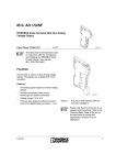
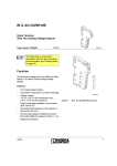
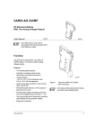
Figure 1
module VARIO AO 1/SF
with connectors to output voltages
Process data update including conversion
time of the digital-to-analog converter < 1 ms
9499-040-67611
1
VARIO AO 1/SF
Local LED Diagnostic and Status Indicators
D
Des. Color Meaning
D
Green Bus diagnostics
UB Green I/O voltage for analog terminals
present (current level)
U B
A O 1 /S F
Terminal Assignment
Conn Terminal Signal
ector Point
1
1.1
U
1
1 .1
1
2
1 .2
1
2
2 .2
2
1 .3
3
3
2 .3
1 .4
4
4
2 .4
1
Figure 2
1 .1
2 .1
1
2
2
1
2 .1
1
1 .2
2
2
2 .2
1 .3
3
3
2 .3
1 .4
4
4
2 .4
2
1
and
2
2.1
1.1
–
I
2.1
I
1.2, 2.2
1.3, 2.3
1.4, 2.4
–
GND
Shield
Assignment
Voltage output
0 V to 10 V
Not used
Current output
0 mA to 20 mA
Current output
4 mA to 20 mA
Not used
Ground
Shield connection
5 5 6 2 B 0 0 2
VARIO AO 1/SF
with appropriate connectors
Installation Instructions
High current flowing through the potential jumpers UM and US leads to a temperature rise of the
potential jumpers and the inside of the terminal. Observe the following instructions to keep the current
flowing through the potential jumpers of the analog terminals as low as possible:
Create a separate main circuit for each analog terminal.
If this is not possible in your application and if you are using analog terminals in a main
circuit together with other terminals, place the analog terminals behind all the other
terminals at the end of the main circuit.
Please note the derating curve on page 12.
2
9499-040-67611
VARIO AO 1/SF
Internal Circuit Diagram
L o c a l b u s
U
U
U
O P C
L +
A N A
L -
2 4 V
+ 7 ,5 V
/ + 1 5 V
R E F
+ 2 4 V (U S )
I0
U
- 2 0
I4
- 2 0
+ 2 4 V (U M )
1
5 5 6 2 C 0 0 3
Figure 3
Internal wiring of the terminal points
Key:
OPC
x x x
X X X
R E F
9499-040-67611
Protocol chip
Amplifier
Optocoupler
Digital-to-analog converter
DC/DC converter with electrical
isolation
Analog output
Reference voltage
1
Analog ground, electrically
isolated from ground of the
potential jumper
3
VARIO AO 1/SF
Electrical Isolation
L o c a l b u s (IN )
U
L
L o c a l b u s (O U T )
B u s in te r fa c e
O P C
(7 .5 V D C )
U
U
U
A N A
(2 4 V D C )
A N A
2 4 V
in te r fa c e
7 .5 V
+ /-1 5 V
F E P o te n tia l
(2 4 V D C )
A
I/O
Figure 4
(7 .5 V D C )
L
A n a lo g o u tp u t
B
E le c tr ic a l is o la tio n
b e tw e e n a re a A a n d B
5 7 3 6 B 0 0 8
Electrical isolation of the individual function areas
Connection Notes
Always connect the analog actuator using shielded, twisted pair cables.
Connect one end of the shielding to PE. At the module, fold the outer cable sheath back
and connect the shield to the terminal via the shield clamp. The clamp connects the shield
directly to FE on the terminal side.
When using cables longer than 10 m (32.81 ft.) in environments prone to interference, we
recommend connecting the shield on the actuator to the FE potential via an RC element.
Typically, the capacitor C should be rated between 1 and 15 nF. The resistor R should be
at least 10 MW.
Use an I/O connector with shield connection when installing the actuator. On the base side
that is not used to connect an actuator, you may use one of the connectors listed in the
ordering data. The appearance of the module differs depending on the output used. This
is shown in Figure 5 and Figure 6 in the top left corner.
4
9499-040-67611
VARIO AO 1/SF
Connection Examples
Use a connector with shield connection when installing the actuator. Figure 5 and Figure 6
show the connection schematically (without shield connector).
Current Output
Voltage Output
D
U B
A O 1
1
2
1
2
1
1 1
1
2
2 2
2
3
3 3
3
4
4 4
4
D
D
U B
A O 1
A O 1
1
U B
2
1
1
2
2
1
2
1 1
1
1
1 1
1
2
2 2
2
2
2 2
2
3
3 3
3
3
3 3
3
4
4 4
4
4
4 4
4
O U T
1
Actuator connected to the voltage
output 0 V to 10 V in 2-wire
technology with shield connection
O U T
Figure 5
A
B
O U T
5 5 6 2 A 0 0 4
5 5 6 2 B 0 0 7
Figure 6
9499-040-67611
Actuator connected to the current
outputs in 2-wire technology with
shield connection
A
Signals for actuator at the current output
0 mA to 20 mA
B
Signals for actuator at the current output
4 mA to 20 mA
5
VARIO AO 1/SF
Programming Data
General
ID code
7Dhex (125dec)
Length code
01hex
Input address area
0 bytes
Output address area
2 bytes
Parameter channel
(PCP)
0 bytes
Register length (bus)
2 bytes
Different Fieldbus Systems
For the programming data of other bus systems, please refer to the appropriate electronic
device data sheet (GSD, EDS).
Process Data Words
Assignment of the Terminal Points to the Process Data Output Word
"Word.bit"
view
Word
Bit
Word x
15 14 13 12 11 10 9
8
7
6
5
"Byte.bit"
view
Byte
Bit
7
Terminal
points
slot 1
Signal
Terminal point 1.1: Voltage output
Shielding (FE)
Terminal point 1.4, 2.4
Terminal
points
slot 2
Signal
Terminal point 1.1: Current output 0 to 20 mA
Terminal point 2.1: Current output 4 to 20 mA
6
5
4
3
3
2
1
0
2
1
0
Byte 1
2
1
0
7
6
5
4
3
Signal reference Terminal point 1.3, 2.3
Signal reference Terminal point 1.3, 2.3
Shielding (FE)
6
Byte 0
4
Terminal point 1.4, 2.4
9499-040-67611
VARIO AO 1/SF
OUT Process Data Output Word
The process data output word specifies the output value in each cycle.
P ro c e s s d a ta w o rd
M S B
L S B
1 5
1 4
1 3
1 2
1 1
1 0
9
8
7
6
5
4
3
2
1
0
A V
5 5 6 2 0 0 0 6
Figure 7
Process data output word
AV
Analog value
MSB
Most significant bit
LSB
Least significant bit
All output values are displayed with 16-bit resolution.
For significant values in the process data word, refer to the following tables.
9499-040-67611
7
VARIO AO 1/SF
Abbreviations used in the following tables:
QS
Quantization step(s)
ORF
Output range final value
MSB
Most significant bit
LSB
Least significant bit
OUT Process Data Output Word for the Voltage Output 0 V to 10 V (Example)
Voltage Output
Analog Value Process Data Output Word
0 V to 10 V
(V)
Hex. Binary (Two's Complement)
MSB
15 14 13 12 11 10 9 8 7 6 5
10 V minus 1 QS
9.99985
FFFF 1 1 1 1 1 1 1 1 1 1 1
10 V minus 2 QS
9.99969
FFFE 1 1 1 1 1 1 1 1 1 1 1
Half ORF
5.0000
8000 1 0 0 0 0 0 0 0 0 0 0
1 QS
0.153 mV
0001 0 0 0 0 0 0 0 0 0 0 0
Zero
0.0000
0000 0 0 0 0 0 0 0 0 0 0 0
3
1
1
0
0
0
2
1
1
0
0
0
LSB
1 0
1 1
1 0
0 0
0 1
0 0
OUT Process Data Output Word for the Current Output 0 mA to 20 mA (Example)
Current Output
Analog Value Process Data Output Word
0 mA to 20 mA
(mA)
Hex. Binary (Two's Complement)
MSB
15 14 13 12 11 10 9 8 7 6 5 4
20 mA minus 1 QS
19.9997
FFFF 1 1 1 1 1 1 1 1 1 1 1 1
20 mA minus 2 QS
19.9994
FFFE 1 1 1 1 1 1 1 1 1 1 1 1
Half ORF
10.000
8000 1 0 0 0 0 0 0 0 0 0 0 0
1 QS
0.305 µA
0001 0 0 0 0 0 0 0 0 0 0 0 0
Zero
0.0000
0000 0 0 0 0 0 0 0 0 0 0 0 0
3
1
1
0
0
0
2
1
1
0
0
0
LSB
1 0
1 1
1 0
0 0
0 1
0 0
OUT Process Data Output Word for the Current Output 4 mA to 20 mA (Example)
Current Output
Analog Value Process Data Output Word
4 mA to 20 mA
(mA)
Hex. Binary (Two's Complement)
MSB
15 14 13 12 11 10 9 8 7 6 5 4
20 mA minus 1 QS
19.99998
FFFF 1 1 1 1 1 1 1 1 1 1 1 1
20 mA minus 2 QS
19.99995
FFFE 1 1 1 1 1 1 1 1 1 1 1 1
Half ORF
12.0000
8000 1 0 0 0 0 0 0 0 0 0 0 0
4 mA plus 1 QS
4.000244
0001 0 0 0 0 0 0 0 0 0 0 0 0
Output range start
4.0000
0000 0 0 0 0 0 0 0 0 0 0 0 0
3
1
1
0
0
0
2
1
1
0
0
0
LSB
1 0
1 1
1 0
0 0
0 1
0 0
8
4
1
1
0
0
0
9499-040-67611
VARIO AO 1/SF
Output Behavior of the Voltage or Current Output
Take the behavior of the output in the event of an error into account when planning your
system.
Switching
Operation/State
of the Supply
Voltage
Marginal
Condition
OUT
Process
Data Word
(hex)
Behavior/Status of the Analog Output
0 V to 10 V
0 mA to 20 mA
4 mA to 20 mA
UANA from
0 V to 24 V
UL = 0 V
xxxx
0V
0 mA
4 mA
UANA from
24 V to 0 V
UL = 7.5 V
xxxx
0V
0 mA
0 mA
Bus in STOP
state
UANA = 0 V
xxxx
0V
0 mA
0 mA
Bus in STOP
state
UANA = 24 V
xxxx
Maintains last value
UANA
Analog supply voltage of the terminal
UL
Supply voltage of the module electronics (communications power)
xxxx
Any value in the range from 0000hex to FFFFhex.
The behavior and status of the output depends on the output used.
9499-040-67611
9
VARIO AO 1/SF
Response of the Control System or Computer to a Hardware Signal for Different Control or
Computer Systems
Signal
Control
or
Computer System
Status After the Switching Operation
OUT Process Data
Output Word
Analog Output
Uout
Iout
NORM*
AEG Schneider
Automation
0000
0V
0 mA/4 mA
BASP
Siemens S5
0000
0V
0 mA/4 mA
CLAB
Bosch
0000
0V
0 mA/4 mA
SYSFAIL
VME
0000
0V
0 mA/4 mA
SYSFAIL
PC
0000
0V
0 mA/4 mA
CLEAR OUT
Moeller IPC
0000
0V
0 mA/4 mA
*
On controller boards for AEG Schneider Automation control systems it is possible to set the
NORM signal so that the OUT process data output word and the analog output maintain the last
value.
The status of the current output depends on the range selected.
Response of the Voltage and Current Outputs to a Control Command of the Controller Board
Command
Status After the Switching Operation
OUT Process Data Output
Word
Analog Output
Uout
Iout
STOP
Maintain last value
Maintain last value
Maintain last value
ALARM STOP (reset)
Maintain last value
Maintain last value
Maintain last value
10
9499-040-67611
VARIO AO 1/SF
Technical Data
General
Housing dimensions (width x height x depth)
24.4 mm x 120 mm x 71.5 mm
(0.961 x 4.724 x 2.815 in.)
Weight
90 g (without connectors), 100 g
(including connectors)
Operating mode
Process data mode with 1 word
Type of actuator connection
2-wire technology
Permissible temperature (operation)
-25°C to +55°C (-13°F to +131°F)
Permissible temperature (storage/transport)
-25°C to +85°C (-13°F to +185°F)
Permissible humidity (operation)
75% on average, 85% occasionally
In the range from -25°C to +55°C (-13°F to +131°F) appropriate measures against
increased humidity (> 85%) must be taken.
Permissible humidity (storage/transport)
75% on average, 85% occasionally
For a short period, slight condensation may appear on the outside of the housing if, for
example, the terminal is brought into a closed room from a vehicle.
Permissible air pressure (operation)
80 kPa to 106 kPa
(up to 2000 m [6562 ft.] above sea level)
Permissible air pressure (storage/transport)
70 kPa to 106 kPa
(up to 3000 m [9843 ft.] above sea level)
Degree of protection
IP 20 according to IEC 60529
Class of protection
Class 3 according to VDE 0106, IEC 60536
Deviations From Common Technical Data That Is Indicated in the User Manual
Mechanical Requirements
Shock test
according to EN 60068-2-27, IEC 60068-2-27
9499-040-67611
15g load for 11 ms, half sinusoidal wave,
three shocks in each space direction and
orientation
25g load for 6 ms, half sinusoidal wave,
three shocks in each space direction and
orientation
11
VARIO AO 1/SF
Interface
Local bus
Through data routing
Power Consumption
Communications power UL
7.5 V
Current consumption from UL
30 mA, typical; 40 mA, maximum
I/O supply voltage UANA
24 V DC
Current consumption at UANA
50 mA, typical; 65 mA, maximum
Total power consumption
1.425 W (typical)
Supply of the Module Electronics and I/O Through Bus Terminal/Power Terminal
Connection method
Potential routing
Derating: Permissible Ambient Temperature Depending on the Current of the Voltage
Jumpers UM and US (Total Current)
6 0
5 5
5 0
4 5
T
A
[° C ]
4 0
3 5
3 0
2 5
2 0
1 5
1 0
5
0
0
2
4
I [A ]
6
TA [°C]
Ambient temperature in °C
I [A]
Current flowing through potential jumpers UM and US (A)
12
8
1 0
5 7 3 6 A 0 0 9
9499-040-67611
VARIO AO 1/SF
Analog Output
Number
1; configured depending on the terminal point
used
Signals/resolution in the process data word (quantization)
Voltage
0 to 10 V
0 to 9.99985 V
0.153 mV/LSB
Current
0 to 20 mA
0 to 19.9997 mA
0.305 µA/LSB
4 to 20 mA
4 to 19.99976 mA
0.244 µA/LSB
Measured value representation
16-bit straight binary
Basic error limit in the current range
±0.05%, typical
Output load
Voltage output
Current output
2 kW, minimum
500 W, maximum
Process data update including conversion time of 1 bus cycle
the digital-to-analog converter
(dependent on the bus configuration); < 1 ms
Slew rate (> 99% of final value)
< 10 µs
Tolerance Behavior and Temperature Response of the Voltage Output
(The error indications refer to the output range final value of 10 V.)
Typical
Maximum
Error at 23°C (73.4°F)
Total offset voltage
±0.03%
±0.05%
Gain error
±0.10%
±0.15%
Differential non-linearity
±0.0012%
±0.003%
±0.15%
±0.25%
Total error at 23°C (73.4°F)
Temperature response at -25°C to +55°C (-13°F to +131°F)
Offset voltage drift TKVO
±10 ppm/K
±65 ppm/K
Gain drift TKG
±30 ppm/K
±35 ppm/K
Total voltage drift TKtot = TKVO + TKG
±40 ppm/K
±100 ppm/K
±0.30%
±0.60%
Total error of the voltage outputs
(-25°C to +55°C [-13°F to +131°F])
Offset error + gain error + linearity error + drift error
9499-040-67611
13
VARIO AO 1/SF
Tolerance Behavior and Temperature Response of the Current Output (0 mA to +20 mA)
(The error indications refer to the output range final value of 20 mA.)
Typical
Maximum
Offset error at 23°C (73.4°F)
Offset current Ioc
±0.05%
±0.15%
Gain error
±0.09%
±0.25%
Differential non-linearity
±0.0012%
±0.003%
±0.15%
±0.25%
Total error at 23°C (73.4°F)
Temperature response at -25°C to +55°C (-13°F to +131°F)
Offset current drift TKIO
±25 ppm/K
±65 ppm/K
Gain drift TKG
±10 ppm/K
±35 ppm/K
Total current drift TKtot = TKIO + TKG
±35 ppm/K
±100 ppm/K
Tolerance Behavior and Temperature Response of the Current Output (4 mA to +20 mA)
(The error indications refer to the output range final value of 20 mA.)
Typical
Maximum
Offset error at 23°C (73.4°F)
Offset current Ioc
±0.15%
±0.45%
Gain error
±0.25%
±0.45%
Differential non-linearity
±0.003%
±0.005%
Total error at 23°C (73.4°F)
±0.25%
±0.46%
Temperature response at -25°C to +55°C (-13°F to +131°F)
14
Offset current drift TKIO
±28 ppm/K
±70 ppm/K
Gain drift TKG
±15 ppm/K
±40 ppm/K
Total current drift TKtot = TKIO + TKG
±43 ppm/K
±110 ppm/K
9499-040-67611
VARIO AO 1/SF
Additional Tolerances Influenced by Electromagnetic Fields
Type of Electromagnetic Interference
Criterion
Typical Relative Deviation of the
Measuring Range Final Value
Electromagnetic fields
Field strength 10 V/m
according to EN 61000-4-3/IEC 61000-4-3
A
< 1%
Fast transients (bursts)
Supply 2 kV, output 1 kV
according to EN 61000-4-4/IEC 61000-4-4
B
< 1%
Conducted interference
Class 3 (test voltage 10 V)
according to EN 61000-4-6/IEC 61000-4-6
A
< 6%
Safety Devices
None
Electrical Isolation/Isolation of the Voltage Areas
The electrical isolation of the logic level from the I/O area is ensured
by the DC/DC converter.
Common Potentials
24 V I/O voltage, 24 V segment voltage, and GND have the same potential. FE is a separate
potential area.
Separate Potentials in the System Consisting of Bus Terminal/Power Terminal and I/O
Terminal
- Test Distance
- Test Voltage
7.5 V supply (bus logic)/24 V supply UANA/I/O
500 V AC, 50 Hz, 1 min.
7.5 V supply (bus logic)/24 V supply UANA/functional earth ground
500 V AC, 50 Hz, 1 min.
24 V supply (I/O)/functional earth ground
500 V AC, 50 Hz, 1 min.
Error Messages to the Higher-Level Control or Computer System
Failure or insufficient communications power UL Yes, I/O error message sent to the bus coupler
9499-040-67611
15
VARIO AO 1/SF
Ordering Data
Description
Order Designation Order No.
Module with one analog output to output either voltage or VARIO AO 1/SF
current signals;
including connectors and labeling fields
KSVC-103-00211
Technical modifications reserved
PMA Prozess- und Maschinen-Automation GmbH
Miramstrasse 87
34123 Kassel
Germany
+49 - (0)561 505 - 1307
+49 - (0)561 505 - 1710
www.pma-online.de
16
9499-040-67611