1
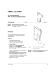
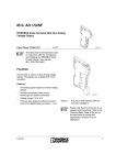
IB IL AO 2/U/BP (-PAC)
D
S
O2
AO
Inline Terminal
With Two Analog Voltage Outputs
AUTOMATIONWORX
Data Sheet
5660_en_02
1
© PHOENIX CONTACT - 04/2007
Description
The terminal is designed for use within an Inline station. It is
used to output analog voltage signals.
Features
–
–
–
–
–
–
–
–
Two analog signal outputs
Actuator connection in 2-wire technology with shield
connection
Voltage ranges:
-10 V to +10 V (13-bit resolution) and
0 V to +10 V (12-bit resolution)
Output value data available in two formats (IB IL and
IB ST)
Parameterizable behavior of the outputs in the event of
an error
Process data update including conversion time of the
digital/analog converter < 1 ms
Very good output driver properties, therefore also
suitable for long actuator cables
Diagnostic indicators
This data sheet is only valid in association with the IL SYS INST UM E user manual or the Inline system manual
for your bus system.
Make sure you always use the latest documentation.
It can be downloaded at www.download.phoenixcontact.com.
A conversion table is available on the Internet at
www.download.phoenixcontact.com/general/7000_en_00.pdf.
This data sheet is valid for the products listed on the following page:
IB IL AO 2/U/BP (-PAC)
Table of Contents
1
Description.................................................................................................................................. 1
2
Ordering Data ............................................................................................................................. 3
3
Technical Data............................................................................................................................ 3
4
Local Diagnostic and Status Indicators and Terminal Point Assignment ................................... 7
4.1
4.2
4.3
4.4
Local Diagnostic and Status Indicators .......................................................................................................... 7
Function Identification .................................................................................................................................... 7
Terminal Point Assignment ............................................................................................................................ 7
Parameterized Default Upon Delivery............................................................................................................ 7
5
Installation Instructions ............................................................................................................... 7
6
Internal Circuit Diagram.............................................................................................................. 8
7
Electrical Isolation....................................................................................................................... 9
8
Connection Notes ....................................................................................................................... 9
9
Connection Example ............................................................................................................................................ 9
10 Connecting Shielded Cables Using the Shield Connector ........................................................10
11 Programming Data .............................................................................................................................................. 11
11.1
11.2
Local Bus (INTERBUS)................................................................................................................................ 11
Other Bus Systems ...................................................................................................................................... 11
12 Process Data .............................................................................................................................12
12.1
12.2
12.3
12.4
Assignment of the Terminal Points to the OUT Process Data Words.......................................................... 12
Assignment of the IN Process Data Words.................................................................................................. 13
OUT Process Data ....................................................................................................................................... 14
IN Process Data ........................................................................................................................................... 15
13 Formats for Representing the Output Values ............................................................................16
13.1
13.2
"IB IL" Format............................................................................................................................................... 16
"IB ST" Format ............................................................................................................................................. 18
14 Output Behavior.........................................................................................................................19
14.1
14.2
14.3
14.4
14.5
Output Behavior During Error-Free Operation
(Normal Operation) ...................................................................................................................................... 19
Output Behavior in the Event of an Error ..................................................................................................... 19
Output Behavior of the Voltage Output ........................................................................................................ 19
Response of the Control System or Computer to a Hardware Signal
for Different Control or Computer Systems .................................................................................................. 20
Response of the Voltage Output to a Control Command of the INTERBUS Controller Board .................... 20
15 Input Behavior ...........................................................................................................................21
16 Parameterization .......................................................................................................................22
5660_en_02
PHOENIX CONTACT
2
IB IL AO 2/U/BP (-PAC)
2
Ordering Data
Products
Description
Type
Order No.
Pcs./Pkt.
Inline terminal with two analog voltage outputs,
complete with accessories (connector and labeling field)
IB IL AO 2/U/BP-PAC
2861467
1
Inline terminal with two analog voltage outputs,
without accessories
IB IL AO 2/U/BP
2732732
1
Type
Order No.
Pcs./Pkt.
IB IL SCN-6 SHIELD-TWIN
2740245
5
The connector listed below is needed for the complete fitting of the IB IL AO 2/U/BP terminal.
Accessories
Description
Connector with six spring-cage connections and shield connection
(green, w/o color print)
Documentation
Description
Type
Order No.
Pcs./Pkt.
"Automation Terminals of the Inline Product Range"
user manual
IL SYS INST UM E
2698737
1
"Configuring and Installing the INTERBUS Inline Product Range"
user manual
IB IL SYS PRO UM E
2743048
1
3
Technical Data
General Data
Housing dimensions (width x height x depth)
12.2 mm x 120 mm x 71.5 mm
Weight
48 g (without connector), 70 g (with connector)
Operating mode
Process data mode with 2 words
Connection method for actuators
2-wire technology
Ambient temperature (operation)
-25°C to +55°C
Ambient temperature (storage/transport)
-25°C to +85°C
Permissible humidity (operation/storage/transport)
10% to 95% according to DIN EN 61131-2
Permissible air pressure (operation/storage/transport)
70 kPa to 106 kPa (up to 3000 m above sea level)
Degree of protection
IP20 according to IEC 60529
Class of protection
Class 3 according to VDE 0106, IEC 60536
Connection data for Inline connector
Connection method
Spring-cage terminals
Conductor cross-section
0.2 mm2 to 1.5 mm2 (solid or stranded), 24 - 16 AWG
Interface
Local bus
Data routing
Transmission Speed
IB IL AO 2/U/BP, IB IL AO 2/U/BP-PAC
5660_en_02
500 kbps
PHOENIX CONTACT
3
IB IL AO 2/U/BP (-PAC)
Power Consumption
Communications power UL
7.5 V
Current consumption at UL
33 mA, typical; 40 mA, maximum (approximately)
I/O supply voltage UANA
24 V DC
Current consumption at UANA
No-load operation (RL > 10 MΩ)
18 mA, typical; 28 mA, maximum
Full load operation (RL = 2 kΩ)
25 mA, typical; 35 mA, maximum
Total power consumption
No-load operation (RL > 10 MΩ)
0.68 W, typical
Full load operation (RL = 2 kΩ)
0.85 W, typical
Supply of the Module Electronics and I/O Through the Bus Coupler/Power Terminal
Connection method
Potential routing
Derating: Permissible Ambient Temperature Depending on the Current of the Potential Jumpers UM and US
(Total Current)
I [A ]
1 0
8
6
4
2
0
4 8
4 9
5 0
5 1
5 2
5 3
5 4
5 5
5 6
T
A
[° C ]
5 6 6 0 0 0 1 2
Above TA = +50°C derating is 2 A/K.
TA
Ambient temperature in °C
I
Current flowing through the potential jumpers UM and US in A
5660_en_02
PHOENIX CONTACT
4
IB IL AO 2/U/BP (-PAC)
Analog Outputs
Number
2
Signal connection method
2-wire technology, single-ended
Signals/resolution in the process data word (quantization)
Voltage
-10 V to +10 V
333.33 µV/LSB
Voltage
0 V to +10 V
333.33 µV/LSB
Representation of output value
-10 V to +10 V
16-bit two's complement
0 V to +10 V
16-bit two's complement
For the representation of the output value in the different formats, please refer to the notes in "Formats for Representing the Output
Values" on page 16.
Smallest DAC quantization step
-10 V to +10 V
2.667 mV (13 bits)
0 V to +10 V
2.667 mV (12 bits)
Basic error limit
±0.02%, typical, of the output range final value
Output load
2 kΩ, minimum
Process data update time including conversion time of the digital/analog
converter
1 INTERBUS cycle (depending on the bus configuration); <1 ms
Signal rise time (slew rate)
10% to 90% of the final value
15 µs, typical
0% to > 99% of the final value
31 µs, typical
Signal rise time (slew rate) (-9.0 V to + 9.0 V)
No-load operation
0.35 V/µs, typical
With ohmic load (RL = 2 kΩ)
0.24 V/µs, typical
With ohmic/capacitive load RL = 2 kΩ / CL = 10 nF
0.24 V/µs, typical
With ohmic/capacitive load RL = 2 kΩ / CL = 220 nF
0.09 V/µs, typical
Transient protection of analog outputs
Yes
Maximum cable length for the LiYCY (TP) cable type,
(shielded twisted power station cable)
500 m
Electrical features of LiYCY (TP)
Inductance
Effective capacitance
N x 2 x 0.5
(N= number of wire pairs,
wire cross-section ≥ 0.5 mm2
0.67 mH/km, typical
120 nF/km, typical
Tolerance Behavior and Temperature Response (Absolute Tolerance Values)
(The tolerance values refer to the output range final value of 10 V.)
Typical
Maximum
Total offset voltage
±0.5 mV
±4.0 mV
Gain error
±2.5 mV
±6.0 mV
Differential non-linearity
±1.3 mV
±3.9 mV
±4.3 mV
±13.9 mV
Tolerance at 23°C
Total tolerance at 23°C
Temperature response at -25°C to +55°C
Offset voltage drift TKVO
±2.1 mV
±5.0 mV
Gain drift TKG
±9.2 mV
±20.0 mV
Total voltage drift TKtot = TKVO + TKG
Total tolerance of the voltage output (-25°C to +55°C)
offset error + gain error + linearity error + drift error
5660_en_02
±11.3 mV
±25.0 mV
±15.6 mV
±38.9 mV
PHOENIX CONTACT
5
IB IL AO 2/U/BP (-PAC)
Tolerance Behavior and Temperature Response (Relative Tolerance Values)
(The tolerance values refer to the output range final value of 10 V.)
Typical
Maximum
Total offset voltage
±0.005%
±0.027%
Gain error
±0.025%
±0.060%
Differential non-linearity
±0.013%
±0.027%
±0.09%
±0.14%
Tolerance at 23°C
Total tolerance at 23°C
Temperature response at -25°C to +55°C
Offset voltage drift TKVO
4 ppm/K
10 ppm/K
Gain drift TKG
18 ppm/K
40 ppm/K
Total voltage drift TKtot = TKVO + TKG
23 ppm/K
50 ppm/K
±0.16%
±0.39%
Total tolerance of the voltage output (-25°C to +55°C)
offset error + gain error + linearity error + drift error
Additional Tolerances Influenced by Electromagnetic Fields
Type of Electromagnetic Interference
Typical Deviation From the Output Range Final Value
(Voltage Output)
Relative
Absolute
Electromagnetic fields;
field strength 10 V/m
according to EN 61000-4-3/IEC 61000-4-3
< ±0.2%
< ±20 mV
Conducted interference
Class 3 (test voltage 10 V)
according to EN 61000-4-6/IEC 61000-4-6
< ±2.8%
< ±280 mV
Safety Equipment
Transient protection of analog outputs
Yes
Electrical Isolation/Isolation of the Voltage Areas
The values are valid for shielded and unshielded twisted actuator cables.
Common Potentials
24 V I/O voltage, 24 V segment voltage, and GND have the same potential. FE is a separate potential area.
Separate Potentials in the System Consisting of Bus Coupler/Power Terminal and I/O Terminal
- Test Distance
- Test Voltage
7.5 V supply (bus logic), 24 V supply UANA / I/O
500 V AC, 50 Hz, 1 min
7.5 V supply (bus logic), 24 V supply UANA / functional earth ground
500 V AC, 50 Hz, 1 min
24 V supply (I/O) / functional earth ground
500 V AC, 50 Hz, 1 min
Error Messages to the Higher-Level Control or Computer System
Failure of or insufficient communications power UL
Yes, I/O error message sent to the bus coupler
Approvals
Information on current approvals can be found on the Internet at www.download.phoenixcontact.com.
5660_en_02
PHOENIX CONTACT
6
IB IL AO 2/U/BP (-PAC)
4
Local Diagnostic and Status
Indicators and Terminal Point
Assignment
D
O -S
A O 2
4.3
Terminal Point Assignment
Terminal
Point
1.1
2.1
1.2, 2.2
1.3, 2.3
1.4, 2.4
4.4
Signal
Assignment
U1
U2
–
AGND
Shield
Voltage output 1
Voltage output 2
Not used
Voltage output ground
Shield connection
Parameterized Default Upon Delivery
By default upon delivery, the parameters are set as follows:
Data format:
Behavior of the outputs in
the event of an error:
Output range:
IB IL
Outputs hold the last value
(Hold)
-10 V to +10 V
The following terminal parameters can be configured
according to your conditions using the process data:
1
2
1 .1
1
1
2 .1
1 .2
2
2
2 .2
1 .3
3
3
2 .3
1 .4
4
4
2 .4
Data format:
Behavior of the outputs in
the event of an error:
Output range:
For parameterization you must switch to
parameterization mode. The procedure is
described in "Parameterization" on page 22.
5 6 6 0 B 0 0 2
Figure 1
4.1
Local Diagnostic and Status Indicators
Desig.
D
O-S
4.2
Terminal with appropriate connector
Color Meaning
Green Diagnostics
Orange Original default state parameterized
IB ST
Outputs are reset to 0 V
(Reset)
0 V to +10 V
5
Installation Instructions
High current flowing through potential jumpers UM and US
leads to a temperature rise in the potential jumpers and
inside the terminal. Observe the following instruction to
keep the current flowing through the potential jumpers of
the analog terminals as low as possible:
Function Identification
Yellow
Create a separate main circuit for each
analog terminal.
If this is not possible in your application and if
you are using analog terminals in a main circuit
together with other terminals, place the analog
terminals behind all the other terminals at the
end of the main circuit.
Please note the derating curve shown on
page 4.
5660_en_02
PHOENIX CONTACT
7
IB IL AO 2/U/BP (-PAC)
6
Internal Circuit Diagram
Key:
OPC
Local bus
OPC
UL+
UANA
UL-
Protocol chip
Optocoupler
µP
SEC
24 V
µ P
Microprocessor
+7,5 V
/ +-15 V
EEPROM
S E C
REF
E E P R O M
Safety circuit
Electrically erasable
programmable read-only memory
x x x
DC/DC converter with electrical isolation
X X X
R E F
Reference voltage
Amplifier
+24 V (US)
+24 V (UM)
Digital/analog converter
1
Analog output
1
5660B003
Figure 2
Analog ground, electrically isolated from
ground of the potential jumper
Internal wiring of the terminal points
Other symbols used are explained in the
IL SYS INST UM E user manual or in the
system manual for your bus system.
5660_en_02
PHOENIX CONTACT
8
IB IL AO 2/U/BP (-PAC)
7
Electrical Isolation
L o c a l b u s (IN )
U
L
L o c a l b u s (O U T )
B u s in te r fa c e
O P C
(7 .5 V D C )
U
U
U
A N A
(2 4 V D C )
in te r fa c e
7 .5 V
1 5 V
F E p o te n tia l
(2 4 V D C )
A
I/O
8
A N A
2 4 V
7 .5 V
1 5 V
Figure 3
(7 .5 V D C )
L
A n a lo g o u tp u ts
B
E le c tr ic a l is o la tio n
b e tw e e n a re a A a n d B
5 6 6 0 A 0 0 8
Electrical isolation of the individual function areas
Connection Notes
9
Connection Example
Analog actuators with a cable length of < 10 m
can be connected using unshielded twistedpair cables.
Use a connector with shield connection when
installing the actuators. Figure 4 shows the
connection schematically (without shield
connector).
Connect analog actuators with a cable length
of > 10 m using shielded twisted-pair cables.
1
O U T 1
Ensure that the braided shield is 15 mm longer
than the strain relief, when connecting a
shielded actuator cable to the I/O connector.
Connect the actuator cable as described in
"Connecting Shielded Cables Using the Shield
Connector" on page 10.
1
1
2
2
3
3
4
4
5 6 6 0 0 0 0 4
Figure 4
5660_en_02
2
O U T 2
Connect one end of the shielding to PE. Fold
the outer cable sheath back and connect the
shield to the terminal via the shield connector
clamp (with strain relief). The clamp connects
the shield directly to FE on the terminal side.
Connection of two voltage actuators with
shield connection using 2-wire technology
PHOENIX CONTACT
9
IB IL AO 2/U/BP (-PAC)
10
Connecting Shielded Cables Using the Shield Connector
A
B
C
a
2 0 m m
(0 .7 8 7 ")
8 m m
(0 .3 1 5 ")
D
E
F
6 7 0 8 A 0 0 2
Figure 5
Connecting the shield using the shield connector
The diameter of the actuator cable is usually
too large to allow the cable to be installed into
the strain relief of the shield connector with
sheathed and folded shield. The connection
procedure for this cable therefore differs from
the connection procedure described in the
IB IL SYS PRO UM E user manual. The
comparative differences with the user manual
are marked in bold text.
Inline wiring is normally without ferrules.
However, it is possible to use ferrules. If
using ferrules, make sure they are
properly crimped.
Wiring Connectors
(According to the User Manual)
•
Connection of the cables according to Figure 5 should be
carried out as follows:
Stripping Cables
•
•
•
•
•
Strip the outer cable sheaths to the desired length (a).
(A)
The desired length (a) depends on the connection
position of the wires and whether the wires should have
a large or small amount of space between the
connection point and the shield connection.
Shorten the braided shield to 20 mm. (A)
Do not fold the braided shield back over the outer
sheath. (B)
Remove the protective foil.
Strip 8 mm off the wires. (B)
5660_en_02
•
Push a screwdriver into the slot of the appropriate
terminal point, so that you can insert the wire into the
spring opening.
Phoenix Contact recommends using an SZF 1-0,6X3,5
screwdriver (Order No. 1204517).
Insert the wire. Remove the screwdriver from the
opening. The wire is now clamped.
For the connector pin assignment, please refer to the table
on page 7.
Connecting the Shield
•
•
Open the shield connector (see user manual). (C)
Place the shield connection clamp in the shield
connector corresponding to the cable width (see user
manual).
PHOENIX CONTACT
10
IB IL AO 2/U/BP (-PAC)
•
•
•
Place the cables in the shield connection. (D)
Push the outer cable sheaths up to the shield
connection clamp. The wires with the braided
shield must be underneath the shield connection
clamp. The braided shield must project
approximately 15 mm over the shield connection
clamp.
Close the shield connector. (E)
Fasten the screws for the shield connector using a
screwdriver. (F)
11
Programming Data
11.1
Local Bus (INTERBUS)
ID code
Length code
Process data channel
Input address area
Output address area
Parameter channel (PCP)
Register length (bus)
11.2
5Bhex (91dec)
02hex
32 bits
4 bytes
4 bytes
0 bytes
4 bytes
Other Bus Systems
For the programming data of other bus
systems, please refer to the appropriate
electronic device data sheet (GSD, EDS).
5660_en_02
PHOENIX CONTACT
11
IB IL AO 2/U/BP (-PAC)
12
Process Data
12.1
Assignment of the Terminal Points to the OUT Process Data Words
(Word.bit) view Byte
Bit
(Byte.bit) view Byte
Bit
Assignment
IB IL format
Assignment
IB ST format
Terminal points Signal
Signal reference
Shielding (FE)
(Word.bit) view Byte
Bit
(Byte.bit) view Byte
Bit
Assignment
IB IL format
Assignment
IB ST format
Terminal points Signal
Signal reference
Shielding (FE)
SB
0
15
14
13
12 11
Byte 0
4
3
10
9
Word 0
8
7
6
5
7
6
5
2
1
0
7
6
5
SB
Channel 1 output value
SB
Channel 1 output value
Terminal point 1.1: voltage output 1
Terminal point 1.3
Terminal point 1.4
15
14
13
12 11
Byte 2
4
3
10
9
Word 1
8
7
6
5
7
6
5
2
1
0
7
6
5
SB
Channel 2 output value
SB
Channel 2 output value
Terminal point 2.1: voltage output 2
Terminal point 2.3
Terminal point 2.4
4
3
Byte 1
4
3
4
3
Byte 3
4
3
2
1
0
2
1
0
0
0
0
2
1
0
2
1
0
0
0
0
Sign bit
In "IB ST" format bits 2 through 0 are irrelevant. Set these bits to "0".
5660_en_02
PHOENIX CONTACT
12
IB IL AO 2/U/BP (-PAC)
12.2
Assignment of the IN Process Data Words
(Word.bit) view Byte
Bit
(Byte.bit) view Byte
Bit
Assignment
(Word.bit) view Byte
Bit
(Byte.bit) view Byte
Bit
Assignment
SB
F
R
H
15
14
13
7
SB
6
5
15
14
13
7
SB
6
5
Word 0
12 11 10 9
8
7
6
5
Byte 0
4
3
2
1
0
7
6
5
Mirrored channel 1 output value
4
3
Byte 1
4
3
Word 1
12 11 10 9
8
7
6
5
Byte 2
4
3
2
1
0
7
6
5
Mirrored channel 2 output value
4
3
Byte 3
4
3
2
1
0
2
F
1
R
0
H
2
1
0
2
F
1
R
0
H
Sign bit
Output data format
Voltage range
Hold/reset
5660_en_02
PHOENIX CONTACT
13
IB IL AO 2/U/BP (-PAC)
12.3
OUT Process Data
The OUT process data words specify the output values in each cycle.
Process data word 0
Process data word 1
MSB
15
LSB
14
13
12
11
10
9
8
7
6
5
4
3
2
1
0
IB IL
OV
SB
15
14
13
12
11
10
SB
9
8
7
6
5
OV
4
3
2
1
0
X
X
X
IB ST
5660B006
Figure 6
SB
OV
X
MSB
LSB
OUT Process data words in IB IL and IB ST formats
Sign bit
Output value
Irrelevant bit
Most significant bit
Least significant bit
Set the irrelevant bits to 0.
5660_en_02
PHOENIX CONTACT
14
IB IL AO 2/U/BP (-PAC)
12.4
IN Process Data
Bits 15 through 3 of the OUT process data words are mirrored in the IN process data words. Bit 15 is the sign bit. Bits 2
through 0 are available as status bits. They contain information about the parameterized behavior of the terminal.
Process data word 0
Process data word 1
MSB
LSB
15
14
13
12
11
10
SB
9
8
OV*
7
6
5
4
3
2
1
0
F
R
H
5660B010
Figure 7
IN process data words
SB
OV*
F
R
H
MSB
LSB
Sign bit
Mirrored output value
Output data format
Voltage range
Hold/reset
Most significant bit
Least significant bit
Bits 2 through 0 have the following meaning:
Bit
2
1
0
Designation
F
R
H
5660_en_02
Meaning
Output data format
Voltage range
Hold/reset
Bit x = 0
IL
-10 V to +10 V
Hold
Bit x = 1
ST
0 V to +10 V
0
PHOENIX CONTACT
15
IB IL AO 2/U/BP (-PAC)
13
Formats for Representing the Output Values
The IB IL AO 2/U/BP terminal has format compatibility with the IB IL AI 2/SF input terminal. This means that it
is possible to use these terminals in multiplexer systems (e.g., IB IL MUX).
"IB IL" is the default format on the terminal. To ensure that the terminal can be operated in previously used ST data formats,
the output value representation can be switched to "IB ST" format.
13.1
"IB IL" Format
The output value is represented in bits 14 through 0. An additional bit (bit 15) is available as a sign bit.
Output value representation in "IB IL" format (15 bits + sign bit)
15
SB
14
SB
OV
13
12
11
10
9
8
7
OV
6
5
4
3
2
1
0
Sign bit
Output value
Significant Output Values in "IB IL" Format
The terminal has two analog output channels that can supply voltages from -10 V to +10 V with a 13-bit resolution.
Output range -10 V to +10 V
Output Data Word
-10 V to +10 V
(Two’s Complement)
UOutput
hex
dec
V
<7FFF
32767
+10.837
>7F00
32512
+10.837
7F00
32512
+10.837
7530
30000
+10.0
0008
8
+2.667 mV
0001
1
+333.33 µV
0000
0
0
FFF8
-8
-2.667 mV
8AD0
-30000
-10.0
8100
-32512
-10.837
<8100
Processed separately:
8001
-32767
+10.837
8080
-32640
-10.837
80xx
(Other)
Hold last value
5660_en_02
Remark
Smallest DAC quantization step
Process data resolution
(Overrange)
(Underrange)
PHOENIX CONTACT
16
IB IL AO 2/U/BP (-PAC)
For the 0 V to 10 V output range only the upper range is used (see Figure 6). The resolution for this range is thus limited to
12 bits.
Bits 2 through 0 are not always considered as "irrelevant bits". For use as a field multiplexer, error messages
as well as overrange or underrange information must be evaluated appropriately. Overrange (8001hex) outputs
10.837 V, underrange (8080hex) 0 V. With an error code (1000 0000 0xxx xxx0bin) the last valid value from the
digital/analog converter is output.
Output range 0 V to 10 V
Output Data Word
0 V to 10 V
(Two’s Complement)
UOutput
hex
dec
V
≤7FFF
32512
+10.837
> 7500
32512
+10.837
7F00
32512
+10.837
7530
30000
+10.0
0008
8
+2.667 mV
0001
1
+333.33 µV
< 0000
0
0
< 8100
Processed separately:
8001
-32767
+10.837
8080
-32640
0
80xx
(Other)
Hold last value
Remark
Smallest DAC quantization step
Process data resolution
(Overrange)
(Underrange)
The 80xxhex range is reserved exclusively for error and message codes.
5660_en_02
PHOENIX CONTACT
17
IB IL AO 2/U/BP (-PAC)
13.2
"IB ST" Format
The output value is represented in bits 14 through 3. Bit 15 is available as sign bit. Bits 2 through 0 are irrelevant.
This format corresponds to the data format used on INTERBUS ST modules.
Output value representation in "IB ST" format (12 bits + sign bit)
15
SB
SB
OV
X
14
13
12
11
10
9
8
7
OV
6
5
4
3
2
X
1
X
0
X
Sign bit
Output value
Irrelevant bit (Set this bit to 0.)
Bits 2 through 0 are not always considered as "irrelevant bits". Values 7FF9hex and 8001hex are recognized as
overrange or underrange and interpreted as 7FF8hex or 8008hex and further processed as normal process data.
In this way MUX-compatibility is ensured. The only exceptions are error codes (with ST only an open circuit).
With this error code (xxxx xxxx xxxx xx1xbin) the last value is maintained.
Significant Output Values in "IB ST" Format
Output range 0 V to 10 V
Output Data Word
(Two’s Complement)
hex
>7FF8
7FF8
4000
0008
< 0000
0 V to 10 V
UOutput
V
9.9975
9.9975
5.0
0.002441
0
Output range -10 V to +10 V
Output Data Word
(Two’s Complement)
hex
>7FF8
7FF8
0008
0000
FFF8
8008
< 8008
5660_en_02
-10 V to +10 V
UOutput
V
9.9975
9.9975
0.002441
0
-0.002441
-9.9975
-9.9975
PHOENIX CONTACT
18
IB IL AO 2/U/BP (-PAC)
14
Output Behavior
14.1
Output Behavior During Error-Free Operation
(Normal Operation)
On power up during normal operation, the output range and
the data format are read using the terminal EEPROM (nonvolatile).
Volatile parameterization is also possible for these settings
as well as for the behavior of the terminal in the event of an
error. This parameterization can be carried out during
runtime by a process data sequence.
14.3
14.2
Output Behavior in the Event of an Error
In the event of an error the outputs behave as set in the
EEPROM (non-volatile) or as subsequently parameterized
(volatile). This means that the outputs hold the last value
(HOLD, default setting) or are reset to 0 (RESET, can be
parameterized).
Output Behavior of the Voltage Output
Take output behavior (in the event of an error) into account when configuring your system!
Switching Operation/State of
the Supply Voltage
Marginal Condition
UANA from 0 V to 24 V
UL = 0 V
xxxx
0V
UANA from 24 V to 0 V
UL = 7.5 V
xxxx
0V
Bus in stop state
UANA = 0 V
xxxx
0V
Bus in stop state
UANA = 24 V
xxxx
Hold last value
xxxx
Hold last value
(default setting) or
0 V (can be parameterized)
Bus reset (e.g., remote bus
cable break)
UANA
UL
xxxx
OUT Process Data Word
(Hexadecimal)
Behavior/Status of the
Analog Output
Analog supply voltage of the terminal
Supply voltage for module electronics (communications power)
Any value in the range 0000hex to FFFFhex
5660_en_02
PHOENIX CONTACT
19
IB IL AO 2/U/BP (-PAC)
14.4
Response of the Control System or Computer to a Hardware Signal for Different Control or Computer
Systems
Signal
Control or Computer System
State After Switching Operation
OUT Process Data Word
(Hexadecimal)
Analog Output
AEG Schneider Automation
0000
0V
BASP
Siemens S5
0000
0V
CLAB
Bosch
0000
0V
SYSFAIL
VME
0000
0V
SYSFAIL
PC
0000
0V
CLEAR OUT
Moeller IPC
0000
0V
NORM*
*
Uout
On controller boards for AEG Schneider Automation control systems it is possible to set the NORM signal so that the
OUT process data word and the analog output hold the last value.
14.5
Response of the Voltage Output to a Control Command of the INTERBUS Controller Board
Command
State After Switching Operation
OUT Process Data Word
(Hexadecimal)
Analog Output
Uout
STOP
xxxx
Hold last value
ALARM STOP (reset)
xxxx
Hold last value (default setting) or
0 V (can be parameterized)
5660_en_02
PHOENIX CONTACT
20
IB IL AO 2/U/BP (-PAC)
15
Input Behavior
When analyzing the input behavior, a distinction is made between normal operation and parameterization mode. Input
behavior in parameterization mode is described in Section "Parameterization" on page 22.
During error-free normal operation, the output data is mirrored in the input words as "acknowledgment" in bits 15
through 3 as soon as it is transmitted to the DAC.
Bits 2 through 0 are available as status bits and are used to display and read the set behavior of the terminal.
As the IB IL AO 2/U/BP terminal only evaluates bits 15 through 3 as data bits in both the IB IL and IB ST format, only these
13 bits are mirrored in the input data word (see notes on error codes, overrange and underrange).
Input data in "IB IL" and "IB ST" formats
15
SB
14
SB
OV*
F
R
H
13
12
11
10
9
8
7
6
5
4
OV*
Sign bit
Mirrored output value
Data format
Output range
Hold/reset
0: IB IL
0: -10 V to +10 V
0: Hold
3
2
F
1
R
0
H
1: IB ST
1: 0 V to 10 V
1: Reset
If an error is detected by the terminal, it is indicated by an error code in the first IN process data word. Possible error codes
can be found in the following table.
Error Codes:
Input Data Word
(Two’s Complement)
hex
8010
Cause
Remedy
This code can only appear in parameterization mode and can have two
causes:
1
Configuration is carried out
Continue configuration
In step 2 of parameterization, this code appears after sending the code
8055hex in the first input word.
It does not indicate an error at this point.
8020
8040
2 Invalid configuration
Check parameterization
DAC voltage falls below the permissible value Check the bus coupler voltage supply;
Check that the potential jumpers are
connecting safely;
I/O error occurs
Replace the terminal
Terminal faulty
Replace the terminal
The error codes overwrite the status bits (bits 2 through 0) with "0". This means that in IB ST data
format, it is also possible to clearly distinguish the data from valid process data.
5660_en_02
PHOENIX CONTACT
21
IB IL AO 2/U/BP (-PAC)
16
Parameterization
By default upon delivery, the terminal parameters are set as
follows:
Data format:
Behavior of the outputs in
the event of an error:
Output range:
IB IL
Outputs hold the last
value (Hold)
-10 V to +10 V
You can configure the following terminal parameters
according to your conditions, using the process data:
Data format:
Behavior of the outputs in
the event of an error:
Output range:
IB ST
Outputs are reset to 0
(Reset)
0 V to +10 V
In order to parameterize the terminal you must change to parameterization mode. In the first process data output word,
transmit codes 8033hex and 8055hex one after the other.
In order not to change accidentally to parameterization mode, you should set bits 2 through 0 to 0 in normal
operation when transmitting process data.
The parameterization is valid for both channels.
Parameterizing the Terminal:
Step 1:
Transmission of code 8033hex in the first OUT process data word.
In bits 15 through 3 of the first IN process data word this code is acknowledged as a normal process
data item.
For every subsequent code which is not equal to 8055hex in the first process data word,
normal operation continues and the code is interpreted as a process data item.
Step 2:
Transmission of code 8055hex in the first OUT process data word.
Acknowledgment takes place via code 8010hex in the first input word.
In this case, this code does not indicate an error, but shows that a configuration word is eventually
expected (in step 3).
For every subsequent code that is not equal to 80xxhex in the first process data word,
parameterization mode is quit.
5660_en_02
PHOENIX CONTACT
22
IB IL AO 2/U/BP (-PAC)
Step 3:
Transmission of parameterization code 1000 0000 1000 p3p2p11bin.
Where px are the terminal parameters:
p3: Data format (0: IB IL; 1: IB ST)
p2: Output range (0: -10 V to 0 V; 1: 0 V to 10 V)
p1: Reset behavior (0: Hold; 1: Reset)
Acceptance of the value is confirmed in bits 15 through 0 of the first input word by mirroring the code.
If an invalid configuration is displayed, code 8010hex appears in the first input data word, which
indicates the error "Invalid Configuration".
This step can be repeated as often as you like.
If a code that is not equal to 80xxhex is transmitted in the first process data word,
parameterization mode is quit without the parameterization taking effect.
Step 4:
In this step you specify whether the parameterization stored in the EEPROM is volatile (dynamic) or
non-volatile (static).
Volatile parameterization: After a power up this setting is no longer available. Subsequent operation
uses the settings stored in the EEPROM.
Transmission of code 8077hex.
Non-volatile parameterization: The parameterization is stored in the EEPROM. After a power up this
parameterization from the EEPROM is used.
Transmission of code 8099hex.
After writing 8077hex or 8099hex the parameterization takes effect and parameterization mode is quit.
This is displayed in the first input word through mirroring of code 8077hex or 8099hex. These values
have a dedicated acknowledgment function. Only the next process data item is processed as normal.
If parameterization was aborted, it is possible to switch to parameterization mode by restarting with step 1. The
orange "O-S" LED on the terminal indicates whether the original configuration is present or if the active
configuration differs from the default configuration of the terminal upon delivery. The LED is on if the default
state has been parameterized.
© PHOENIX CONTACT 04/2007
5660_en_02
PHOENIX CONTACT GmbH & Co. KG • 32823 Blomberg • Germany
Phone: +49-(0) 5235-3-00 • Fax: +49-(0) 5235-3-4 12 00
www.phoenixcontact.com
23