Download CM-iGLX User Manual
Transcript
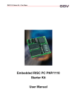
CM-iGLX
Computer-On-Module
Reference Guide
1
Table of Contents
1.
Revision Notes ............................................................................................................. 4
2.
Overview...................................................................................................................... 5
2.1. HIGHLIGHTS ..........................................................................................................5
2.2. BLOCK DIAGRAM ..................................................................................................6
2.3. FEATURES..............................................................................................................7
2.4. GENERAL DESCRIPTION .........................................................................................9
2.5. AMD "LX" CPU CORE ARCHITECTURE .............................................................10
2.6. NAND FLASH DISK ............................................................................................11
3.
Peripherals and Functions ....................................................................................... 12
3.1. WATCHDOG .........................................................................................................13
3.2. REAL-TIME CLOCK..............................................................................................13
3.3. DISPLAY CONTROLLER ........................................................................................15
3.4. GENERAL PURPOSE INPUT / OUTPUT ...................................................................18
3.5. PCI BUS HOST BRIDGE .......................................................................................19
3.6. AC97 INTERFACE ................................................................................................23
3.7. LPC - LOW PIN COUNT INTERFACE .....................................................................25
3.8. SERIAL PORTS .....................................................................................................25
3.9. USB PORTS .........................................................................................................27
3.10. AUDIO INTERFACE ...............................................................................................27
3.11. TOUCH SCREEN CONTROLLER .............................................................................29
3.12. HARD DISK CONTROLLER - PARALLEL ATA .......................................................30
3.13. 10/100 MBIT ETHERNET PORT ............................................................................32
3.14. JTAG INTERFACE ................................................................................................35
3.15. CLOCKS, TIMERS, RESET, WRITE PROTECT, BOOT, POWER MANAGEMENT .......36
3.16. SMBUS (I2C) ......................................................................................................37
3.17. POWER SUPPLY PINS ...........................................................................................37
3.18. RESTRICTIONS ON USING PULL-UPS / PULL-DOWNS............................................39
3.19. UNCONNECTED PINS............................................................................................39
4.
Interface Connectors ................................................................................................ 41
4.1. CONNECTOR TYPE ...............................................................................................41
4.2. CONNECTOR LAYOUT ..........................................................................................42
4.3. CONNECTORS PINOUT .........................................................................................43
5.
MEMORY and I/O mapping ................................................................................... 49
5.1. MEMORY SPACE USAGE IN THE FIRST 1MB..........................................................49
5.2. MEMORY SPACE USAGE ABOVE FIRST 1MB.........................................................49
5.3. I/O SPACE USAGE ................................................................................................50
5.4. BIOS FLASH MAPPING ........................................................................................51
6.
Power Consumption ................................................................................................. 52
2
7.
Performance Benchmarks........................................................................................ 52
8.
Operating Temperature Ranges.............................................................................. 53
3
1. Revision Notes
Date
30-Jun-2006
27-Nov-2006
06-May-2007
27-Nov-2007
26-Dec-2007
Description
Preliminary release
Audio sampling rate errata published
UCB1400 (audio codec) reference replaced by WM9715L, as design
change. Functionality remains the same.
Made clarifications about SMbus signals.
Added Power sequence notes
Published WiFi specifications in datasheet section
Please check for a newer revision of this manual in CompuLab's website http://www.compulab.co.il, following [Developer] >> [iGLX] links. Compare the revision
notes of the updated manual from the website with those of the printed version you have.
4
CM-iGLX Embedded PC Module
2. Overview
2.1.
Highlights
•
Full Featured PC-Compatible
Computer-On-Module
•
AMD Geode LX800 CPU at 500
MHz, 256 KB cache
•
256 Mbyte DDR
•
512 Mbyte Flash Disk
•
Graphics Controller for LCD and
FPM, up to 1920 x 1440
•
General purpose bus and optional
PCI, LPC, AC97 busses
•
WLAN / WiFi 802.11g Interface
•
Video Input Port
•
Sound codec with speaker and
microphone support
•
Touchscreen Controller
•
Up to 3 host USB-2 ports, including
keyboard and mouse support
•
Serial ports, GPIO, hard-disk
interface
•
100 Mbps Ethernet port
•
Low power consumption
•
Small size - 68 x 58 mm
•
Interchangeable with other
modules via CAMI connectors
Note: Some features are optional. Values
are specified at their maximum.
CompuLab Ltd.
The CM-iGLX packs up-to-date
technologies into the most compact,
lightweight PC-on-module available in the
market. Its on-board resources suffice to
smoothly run operating systems such as
Linux and Windows XP / CE, while it is just
as small as a credit card and can run on a
battery. These, in addition to the module's
low cost, make it an ideal building block for
any embedded application.
The feature set of the CM-iGLX combines a
32-bit X86-compatible CPU, DDR, Flash
Disk and vital computing peripherals. For
embedded applications, the CM-iGLX
provides a 32-bit PCI bus, 100Mbit Ethernet,
serial ports, general purpose I/O lines and
many other essential functions. The user
interface is supported by an enhanced
graphics controller, touchscreen, USB
interface for keyboard / mouse and Audio
system. An integrated WLAN (WiFi)
interface implements 802.11g industry
standard wireless connectivity.
The standardized CAMI ("CompuLab's
Aggregated Module Interface") connectors of
the CM-iGLX module allow
interchangeability with other Computer-OnModule's available from CompuLab, enabling
the flexibility required in a dynamic market
where application requirements can change
rapidly.
5
CM-iGLX Embedded PC Module
Block Diagram
Geode LX800 MPU, 500 MHz
5.0V
3.3V
Power
Supply
CLOCKs
Geode LX Core
FPU
MMU
64 KB L1 D-cache
64 KB L1 I-cache
128 KB L2 Cache
DDR, 64-bit
128 - 256 MB
DRAM
Controller
128-bit AES
Security
Video input
2D
Graphics
Processor
Video Input
Port
Display
Controller
PCI
Interface
RGB DAC
TFT interface
CRT interface
PCI Bus
HDD interface
GeodeLink
10/100BaseT
LEDs
Ethernet Ctrl.
RTL8139D
(option E )
BOOT ROM
IDE ATA-100
LPC Controller
LPC bus
2 x UARTs
I/O Ports
I/O lines
COM-A
RS232
SMbus / I2C
USB1,2,(3)
WiFi Interface
RT2571
(option W)
4 x USB-2 Host
Flash Disk
Controller
CS5536
COM-B
Antenna
Connector
2.2.
RTC & CMOS
AC97 Ctrl.
Audio
Touchscreen
NAND Flash Disk
128 - 512 MB
(option N )
CompuLab Ltd.
BAT
AC97 bus
Spkr & Mic
ResistiveTS
UCB1400 (opt AT)
6
CM-iGLX Embedded PC Module
2.3.
Features
The "Option" column specifies the P/N code required to have the particular feature.
"+" indicates that the feature is always available.
CPU, Memory and Busses
Feature
CPU
DRAM
BIOS Flash
NAND Flash Disk
External Busses
AC97
PCI bus
LPC bus
CompuLab Ltd.
Specifications
AMD LX800 / LX700 CPU, Pentium compatible, up to 500
MHz.
64 + 64 KB L1 and 128 KB L2 cache.
DMA and Interrupt controllers, Timers
128 / 256 MB DDR, 333 MHz, 64-bit
1/2 Mbyte, on-board reprogrammable
128 / 512 MB, more in future. 10 MB/s transfer rate.
PCI, LPC, AC97
AC97 Rev 2.3 compliant
32-bit, rev 2.2-compliant, 132 MB/s, 3.3-volt tolerant
Arbiter and clock for one or two masters
Host, 33 MHz, Intel LPC v1.0 compatible
Option
C
D
+
N
+
+
+
+
7
CM-iGLX Embedded PC Module
Peripherals
Feature
Graphics
Controller
Display Interface
Video Input Port
USB
Serial Ports
GPIO
Hard Disk Interf.
Kbrd & Mouse
Ethernet
Audio codec
Touchscreen ctrl.
RTC
WiFi
Encryption unit
Specifications
Option
Resolution up to 1920 x 1440 x 32 bpp @ 85Hz, frame buffer in
+
system memory, 2D graphic processor
LCD - 18-bit parallel RGB for TFT panels
+
CRT - 24-bit analog RGB for CRT / FPM
+
VESA1.1 & VESA2.0 standard, BT.601, BT.656, 8-bit port,
+
150 MHz data rate
Three Host USB 2.0 ports, 480 Mbps, EHCI / OHCI compliant
+
Two UART's, Rx & Tx only
+
4 lines dedicated + 4 lines shared
+
IDE interface, UDMA ATA-100 mode
+
USB or redirection from serial port
+
100 Mb/s, Activity LED's. RTL8139
E
Wolfson WM9715L controller, AC97 interface, mono
microphone input, stereo line input and 25 mW output for active AT
speakers
A part of the WM9715L chip. Supports resistive touch panels
AT
Real Time Clock, powered by external lithium battery
+
Ralink RT2571chipset, 802.11b/g, USB internal interface
W
128 bit DMA based crypto acceleration block up to 44 Mbps
+
Electrical, Mechanical and Environmental Specifications
Supply Voltage
Power consumption
Dimensions
Weight
MTBF
3.3V
3 - 5 W, depending on configuration and CPU speed
68 x 58 x 8 mm
37 gram
> 100,000 hours
Commercial : 0o to 70o C
Operation
Extended : -20o to 70o C
temperature (case)
Industrial : -40o to 85o C
Storage temperature -40o to 85o C
10% to 90% (operation)
Relative humidity
05% to 95% (storage)
Shock
50G / 20 ms
Vibration
20G / 0 - 600 Hz
CompuLab Ltd.
8
CM-iGLX Embedded PC Module
Connectors
General Description
The CM-iGLX is a miniature, single-board computer packed as a module. It contains a
CPU, chipset, memory, flash disk and peripherals. All interface functions of the CMiGLX are routed through miniature high-density connectors, designed for piggyback
attachment to a custom baseboard, as shown in the picture below.
54 mm
m
m
CM-iGLX
MODULE
68
2.4.
3 x 140 pin, 0.6 mm. Insertion / removal up to 50 cycles
58 mm
CM-iGLX
Example of the custom card with attached
CM-iGLX module
BASEBOARD
1.8 x 2.1
CompuLab Ltd.
9
CM-iGLX Embedded PC Module
2.5.
AMD "LX" CPU Core Architecture
The x86 CPU core consists of an Integer Unit, cache memory subsystem, and Floating
Point Unit. The Integer Unit contains the instruction pipeline and associated logic. The
memory subsystem contains the instruction and data caches, translation look-aside buffers
(TLBs), and an interface to the GeodeLink Interface Units (GLIUs).
The instruction set supported by the core is a combination of Intel’s Pentium, the AMD-K6
microprocessor and the Athlon FPU, and the AMD Geode LX processor specific
instructions. Specifically, it supports the Pentium, Pentium Pro, 3DNow technology for the
AMD-K6 and Athlon processors, and MMX instructions for the Athlon processor. It
supports a subset of the specialized Geode LX processor instructions including special
SMM instructions. The CPU Core does not support the entire Katmai New Instruction
(KNI) set as implemented in the Pentium 3. It does support the MMX instructions for the
Athlon processor, which are a subset of the Pentium 3 KNI instructions.
AMD LX processor architecture is relatively simple: instructions are issued, executed and
retired in order, one instruction issued per clock. On the other hand, the design is highly
optimized to achieve high performance in the targeted environment. Some of the
significant features providing this performance are:
Large on-chip caches and TLB’s:
The AMD “LX” CPU implements large caches and TLB’s that significantly reduce stalls
due to bus traffic:
Two 64-KB primary (L1) caches with 16-way associativity
A 4-way 128-KB unified level-2 (L2) victim cache
A 16-entry TLB (TLB1) with fully associativity
A 64-entry TLB (TLB2) with 2-way associativity
Extensive features to minimize bus stalls:
Full memory type range registers (MTRR’s)
A non-stalling write-allocate implementation
Efficient prefetch and branch prediction
Integrated FPU that supports the MMX® and AMD 3DNow!™ instruction sets
Fully pipelined single precision FPU hardware with microcode support for higher
precision
CompuLab Ltd.
10
CM-iGLX Embedded PC Module
AMD "LX" processor Architecture Block Diagram
Security Block
The Geode LX processor has an on-chip AES 128-bit crypto acceleration block capable of
44 Mbps throughput on either encryption or decryption at a processor speed of 500 MHz.
The AES block runs asynchronously to the processor core and is DMA-based. The AES
block supports both EBC and CBC modes. The initialization vector for CBC mode can be
generated by the True Random Number Generator (TRNG). The TRNG is addressable
separately and generates a 32-bit random number.
2.6.
NAND Flash Disk
CM-iGLX contains on-board NAND flash disk, supported by all operating systems
available from CompuLab. The Flash Disk behaves exactly like a regular hard disk drive;
however, it doesn't have any moving parts.
The NAND Flash is a block device - optimized for block read and write operations rather
than for random access. CM-iGLX also contains on-board Flash Disk Controller, which
takes care for translation between operating system commands and NAND flash read/write
operations. The controller connected to CPU through USB port. In addition to the flash
disk emulation, the controller implements error correction (ECC), write protection and
caching for improved performance.
The NAND Flash size is 128 or 512 Mbytes. The CM-iGLX is designed for upward
compatibility with future NAND Flash devices of larger capacity.
Performance
Read
Write
5000 KB/s
840 KB/s
CompuLab Ltd.
11
CM-iGLX Embedded PC Module
3. Peripherals and Functions
Interrupt Channel Mapping
IRQ
IRQ0
IRQ1
IRQ2
IRQ3
IRQ4
IRQ5
IRQ6
IRQ7
IRQ8
IRQ9
IRQ10
IRQ11
IRQ12
IRQ13
IRQ14
IRQ15
I/O Device
PIT 0
Slave controller cascading
COM B, off-board PCMCIA
COM A, off-board PCMCIA
PCI
Off-board PCMCIA
Real-time clock
PCI
PCI
PCI
Floating point error
IDE
Off-board PCMCIA
Priority
On-board usage
P1
P2
—
P11
P12
P13
P14
P15
P3
P4
P5
P6
P7
P8
P9
P10
always
always
always
always
always
-
If the IRQ is used by the on-board device, disabling the device will free the IRQ. If the onboard device cannot be disabled, then the IRQ is always assigned for on-board usage and is
therefore marked accordingly in the table above. PCI interrupts support sharing, i.e., the
same interrupt may be used by several on-board and off-board devices.
Serial IRQ
Serial IRQ allows a single signal line to be used to report the legacy ISA interrupt requests.
Interrupt sharing is allowed on Serial IRQ interfaces only for the devices external to the
chipset. The following interrupts are external to the chipset and are therefore potentially
available on the Serial IRQ interface: IRQ1, IRQ6, IRQ7, IRQ12 and IRQ15. The serial
IRQ interface is a synchronous interface. Data is clocked by the system's PCI clock.
CompuLab Ltd.
12
CM-iGLX Embedded PC Module
Serial IRQ interface
3.1.
Signal
Pin
Type
SERIRQ
P2-13
I/O
Description
The routing for this signal must follow PCI layout/routing
rules
Watchdog
A watchdog is available on the CS5536 companion chip. The timer has a 16-bit counter
that counts up until the programmed value using 1 Hz clock. The comparator is loaded
with an initial value and start counts from zero. On reaching the programmed value, it
generates a system reset. The timer’s status can be read and updated at any time. The
watchdog can be de-activated and re-activated. A driver and sample application for
watchdog operation is provided in the O/S packages.
3.2.
Real-Time Clock
The RTC is compatible with the standard used in PC/AT systems. The RTC consists of a
time-of-day clock with an alarm interrupt and a 100-year calendar. The clock / calendar
has a programmable periodic interrupt, 242 bytes of static user RAM and can be
represented in either binary or BCD. The RTC includes the following features:
Counting of seconds, minutes and hours of the day
Counting of days of the week, date, month and year
12–24 hour clock with an am/pm indicator in 12-hour mode
242 bytes of general-purpose RAM
Three separate software-maskable and testable interrupts: (1) time-of-day alarm is
programmable to occur from once-per-second to once-per-month, (2) periodic
interrupts can be configured to occur at rates from 3.9 ms to 500 ms, and (3) updateended interrupt provides cycle status.
The voltage monitor circuit checks the voltage level of the backup lithium battery
and sets a bit when the battery voltage level falls below specification.
The internal RTC reset signal performs a reset when power is applied to the RTC
core.
The RTC uses a dedicated lithium backup battery when the rest of the card is completely
powered down (RTC-only mode). The RTC can continue operating even when the rest of
the card is not powered. The battery should be connected to the VCC-RTC input of the
CM-iGLX's interface connector. The equivalent RTC supply circuit is shown in the
figure below.
CompuLab Ltd.
13
CM-iGLX Embedded PC Module
3.3V
VT8237
CS5536
South Bridge
RTC VCC PIN
VCC-RTC
VCC-RTC
Low-drop
shottky diode
VCC-RTC Input Current
(Rest of the card powered down)
CM-iGLX
CM-iVC3
Typical
2 µA
Max
6 µA
Storing of BIOS Settings
The CM-iGLX's BIOS has two sets of stored settings:
1.
Current settings stored in CMOS memory, backed-up by battery as described
above. The battery is not located on the CM-iGLX itself, but rather should be
provided on the baseboard. When the CMOS is not powered, the settings it
saves are lost.
2.
Default settings saved in Flash memory. These settings remain valid when the
card is not powered, even in the absence of battery backup. The user can
update the Flash default settings to any values desired.
On startup, the BIOS checks if valid CMOS settings are available. If they are,
BIOS takes the settings from the CMOS. Flash defaults are ignored in that case. If
CMOS settings are not valid (i.e., were erased), BIOS uses the default settings
from the Flash. In this case, BIOS also copies the default settings from the Flash to
the CMOS, to make its contents valid.
CompuLab Ltd.
14
CM-iGLX Embedded PC Module
3.3.
Display Controller
The powerful Display Controller of the CM-iGLX contains a comprehensive set of features
required for multimedia applications:
Integrated Graphics / Video Accelerator
Optimized Unified Memory Architecture (UMA)
Hardware frame buffer compression
2 to 128 MB frame buffer using system memory
Simultaneous CRT / TFT Support
Resolutions up to 1920x1440x32 bpp at 85 Hz, or
up to 1600x1200x32 bpp at 100 Hz
Supports down to 7.652 MHz Dot Clock (320x240QVGA)
Hardware legacy VGA
Hardware supported 48x64 32-bit cursor with alpha blending
Extensive Display Support
Integrated Dot Clock PLL with up to 350 MHz clock
Integrated 3x8-bit DAC with up to 350 MHz sampling
Video Support
Supports video scaling and mixing
Hardware video up/down scalar
Graphics/video alpha blending and color key mixing
TFT outputs
Legacy RGB mode
VESA 1.1, 2.0
Video Input Port
VESA 1.1, 2.0 and BT.601, BT.656 compliant, 150 MHz (excludes host interface).
Standard 9 pin interface (8 data + clock)
8-bit BT.656 video
VIP 1.1 compatible mode (8 bit)
8-bit BT.601 type input video with HSYNC and VSYNC
CompuLab Ltd.
15
CM-iGLX Embedded PC Module
Display Controller Block Diagram
CompuLab Ltd.
16
CM-iGLX Embedded PC Module
LCD Panel Interface Signals
Signal
Pin
Type
LCD-B0
LCD-B1
LCD-B2
LCD-B3
LCD-B4
LCD-B5
LCD-G0
LCD-G1
LCD-G2
LCD-G3
LCD-G4
LCD-G5
LCD-R0
LCD-R1
LCD-R2
LCD-R3
LCD-R4
LCD-R5
LCD-SCK
LCD-FRM
LCD-LP
LCD-DE
LCD-VDDEN
P3-126
P2-95
P2-97
P2-100
P2-99
P2-102
P2-101
P2-104
P2-106
P2-105
P2-108
P2-107
P3-128
P2-109
P2-113
P2-116
P2-118
P2-117
P2-112
P2-111
P2-96
P2-114
P3-130
O
O
O
O
O
O
O
O
O
O
O
O
O
O
O
O
O
O
O
O
O
O
O
Description
LCD Panel Data Bus.
Display Data Clock. Pixel clock for flat panel data.
Frame Sync. Flat Panel equivalent of VSYNC.
Line Sync. Flat Panel equivalent of HSYNC.
Display Enable signal (DE) for TFT Panels.
Power sequencing control for panel driver electronics
voltage VDD.
CRT Interface Signals
Signal
Pin
Type
CRT-HSYNC
CRT-VSYNC
CRT-R
CRT-G
CRT-B
P3-129
P3-140
P3-132
P3-136
P3-133
O
O
O
O
O
CompuLab Ltd.
Output
Drive
1/4 mA
1/4 mA
19 mA
19 mA
19 mA
Description
CRT Horizontal Sync
CRT Vertical Sync
CRT analog video outputs from the
internal color palette DAC. The DAC is
designed for a 37.5 ohm equivalent load on
each pin (e.g., 75 ohm resistor on the
board, in parallel with the 75 ohm CRT
load)
17
CM-iGLX Embedded PC Module
Video Input Port interface signals
Signal
VIP-CLK
VIP-D0
VIP-D1
VIP-D2
VIP-D3
VIP-D4
VIP-D5
VIP-D6
VIP-D7
3.4.
Pin
Type
P3-88
P3-80
P3-82
P3-84
P3-90
P3-92
P3-94
P3-96
P3-89
I
I
I
I
I
I
I
I
I
Description
Video Input Port clock input
Video Input Port data input
Video Input Port data input
Video Input Port data input
Video Input Port data input
Video Input Port data input
Video Input Port data input
Video Input Port data input
Video Input Port data input
General Purpose Input / Output
The CS5536 companion chip integrated in the CM-iGLX provides 8 general purpose I/O
pins (GPIO’s) – four dedicated and the other four shared with alternative functions.
GPIO sample code is available in o/s packages provided by CompuLab.
The dedicated GPIO’s are:
Signal
GPIO6
GPIO5
GPIO27
GPIO25
Pin
Type
Remarks
P1-13
P1-16
P1-15
P1-18
I/O
I/O
I/O
I/O
Autosense weak PU/PD
Autosense weak PU/PD
Configurable PU/PD, controls Power Led
Configurable PU/PD
GPIO's shared with alternative functions:
Default
configuration
TIMER-OUT
[GPIO1]
LPC-LDRQ
[GPIO20]
SERIRQ
[GPIO21]
PME
[GPIO26]
Pin
Type
Remarks
On board
usage
P3-61
I/O
Configurable PU
-
P2-17
I/O
PU 8.2k
-
P2-13
I/O
PU 8.2k
-
P1-17
I/O
Configurable PU/PD
+
* GPIO references are specified according to enumeration used in CS5536 manual.
CompuLab Ltd.
18
CM-iGLX Embedded PC Module
3.5.
PCI Bus Host Bridge
The CM-iGLX contains an integrated PCI bus host bridge allowing interface to any PCI
bus Revision 2.2-compliant master or target device. The PCI host bridge on the CM-iGLX
has the following functionality:
Master controller - Allows the CPU to be a master on the PCI bus. The CPU can
generate transactions to configure the PCI host bridge, as well as all external devices on
the PCI bus. The CPU can also generate memory and I/O read and write transactions on
the PCI bus.
Target controller - Allows external PCI bus masters to access the CM-iGLX's onboard DRAM.
Features:
33 MHz operation
Target support for fast back-to-back transactions
Arbiter support for one or two external PCI bus masters
Write gathering and write posting for in-bound write requests
Virtual PCI header support
Delayed transactions for in-bound read requests
Zero wait state operation within a PCI burst
Dynamic clock stop/start support
Capable of handling out-of-bounds transactions immediately after reset
PCI-2.2 compliant, 32 bit 3.3V PCI interface
PCI Clock System
The clock source is from an on-board oscillator. The CM-iGLX acts as a 'motherboard',
providing clocks to all other parts of the application. If a developer needs to synchronize
PCI bus operation with another clock source from a custom baseboard, then a PCI-to-PCI
bridge should be used. (Suitable bridges are available from PLX and other
manufacturers.)
The PCI standard allows up to a 2ns clock skew. In order to minimize the initial skew
value, the internal feedback path is designed with a 10 cm trace length - to create the
initial delay. Feedback is provided to the clock generation block of the PCI bridge. The
timing of all internal clock references is shifted accordingly. In other words, PCI signals
are pre-compensated for an external clock trace length of 10 cm. The maximum allowed
length of the external clock trace is:
10 cm (pre-compensated) + 30 cm (max propagation delay for a skew less than 2ns)
CompuLab Ltd.
19
CM-iGLX Embedded PC Module
PCI Bus Signals
Signal
PCI-AD0
PCI-AD1
PCI-AD2
PCI-AD3
PCI-AD4
PCI-AD5
PCI-AD6
PCI-AD7
PCI-AD8
PCI-AD9
PCI-AD10
PCI-AD11
PCI-AD12
PCI-AD13
PCI-AD14
PCI-AD15
PCI-AD16
PCI-AD17
PCI-AD18
PCI-AD19
PCI-AD20
PCI-AD21
PCI-AD22
PCI-AD23
PCI-AD24
PCI-AD25
PCI-AD26
PCI-AD27
PCI-AD28
PCI-AD29
PCI-AD30
PCI-AD31
CompuLab Ltd.
Pin
Type
P2-20
P2-22
P2-21
P2-24
P2-23
P2-25
P2-28
P2-27
P2-29
P2-32
P2-34
P2-33
P2-36
P2-35
P2-37
P2-40
P2-51
P2-54
P2-53
P2-56
P2-58
P2-57
P2-60
P2-59
P2-64
P2-63
P2-66
P2-65
P2-68
P2-70
P2-69
P2-72
B
B
B
B
B
B
B
B
B
B
B
B
B
B
B
B
B
B
B
B
B
B
B
B
B
B
B
B
B
B
B
B
Description
PCI Address Data Bus
20
CM-iGLX Embedded PC Module
PCI Bus Signals (continued)
Signal
Pin
Type
Description
PCI-CBE0#
P2-30
B
PCI-CBE1#
P2-39
B
PCI-CBE2#
P2-52
B
PCI-CBE3#
P2-61
B
PCI-DEVSEL#
P2-45
B
PCI-FRAME#
P2-49
B
PCI-INTA#
PCI-INTB#
PCI-INTC#
PCI-INTD#
PCI-IRDY#
P2-6
P2-8
P3-20
P3-17
P2-47
I
I
I
I
B
Command or Byte-Enable Bus functions: (1) as a
time-multiplexed bus command that defines
transaction type on the AD bus, or (2) as byte enables:
CBE0 for AD7–AD0
Command or Byte-Enable Bus functions: (1) as a
time-multiplexed bus command that defines
transaction type on the AD bus, or (2) as byte enables:
CBE1 for AD15–AD8
Command or Byte-Enable Bus functions: (1) as a
time-multiplexed bus command that defines
transaction type on the AD bus, or (2) as byte enables:
CBE2 for AD23–AD16
Command or Byte-Enable Bus functions: (1) as a
time-multiplexed bus command that defines
transaction type on the AD bus, or (2) as byte enables:
CBE3 for AD31–AD24
Device Select is asserted by the target when it has
decoded its address as the target of the current
transaction. This signal is pulled up on-board with an
8.2K resistor.
Frame is driven by the transaction initiator to indicate
the start and duration of the transaction.
This signal is pulled up on-board with an 8.2K
resistor.
PCI Interrupt Requests is asserted to request an
interrupt.
PCI-PAR
P2-42
B
PCI-PERR#
P2-44
B
PCI-PCIRST#
P1-137
O
CompuLab Ltd.
Initiator Ready is asserted by the current bus master
to indicate that data is ready on the bus (write) or that
the master is ready to accept data (read). This signal is
pulled up on-board with an 8.2K resistor.
PCI Parity is driven by the initiator or target to
indicate parity on the AD31–AD0 and CBE3–CBE0
busses.
Parity Error is not supported. This signal is pulled
up on-board with an 8.2K resistor.
Reset is asserted to reset the PCI devices.
21
CM-iGLX Embedded PC Module
Signal
Pin
Type
Description
PCI-SERR#
P2-41
I
PCI-STOP#
P2-46
B
PCI-TRDY#
P2-48
B
PCI-REQ0#
PCI-REQ1#
P2-1
P2-18
I
PCI-GNT0#
PCI-GNT1#
P2-3
P2-5
O
PCI-CLK0
PCI-CLK1
PCI-CLK2
P2-16
P3-16
P3-24
O
System Error is not supported. This signal is pulled
up on-board with an 8.2K resistor.
Stop is asserted by the target to request that the
current bus transaction be stopped. This signal is
pulled up on-board with an 8.2K resistor.
Target Ready is asserted by the currently addressed
target to indicate its ability to complete the current
data phase of a transaction.
This signal is pulled up on-board with an 8.2K
resistor.
Bus Request is asserted by the master to request
access to the bus. PCI_REQ1# is available only if onboard Ethernet chip is not assembled.
Bus Grant is asserted by the CM-iGLX to grant
access to the bus. PCI_GNT1# is available only if onboard Ethernet chip is not assembled.
PCI Bus Clock Output is a 33-MHz clock for PCI
bus devices. This signal is derived from an onboard
33MHz source. Clock edge position is internally
compensated in order to reduce skew to a minimum.
Notes
1.
2.
Output drive and maximum load specifications are according to PCI bus Standard
Rev-2.2.
PCI Bus inputs / outputs inputs are 3.3V-level
CompuLab Ltd.
22
CM-iGLX Embedded PC Module
PCI resource map
Device
CM-iGLX Host bridge
CM-iGLX display controller
CM-iGLX Encryption Device
ATX baseboard PCI Slot
ATX baseboard CardBus bridge skt. A
ATX baseboard CardBus bridge skt. B
ATX baseboard Ethernet
CM-iGLX Ethernet
CM-iGLX internal ISA bridge
CM-iGLX IDE controller
CM-iGLX audio controller
USB 1.1 controller
USB 2.0 controller
IDSEL
line
AD11
AD11
AD11
AD18
AD19
AD19
AD20
AD23
AD25
AD25
AD25
AD25
AD25
PCI dev. / func.
0x01,func.0
0x01, func. 1
0x01, func. 2
0x08, func. 0
0x09, func. 0
0x09, func. 1
0x0A, func. 0
0x0D,func. 0
0x0F, func. 0
0x0F, func. 2
0x0F, func. 3
0x0F, func. 4
0x0F, func. 5
IRQ
11
11
10,11
10
11
11
11
14
11
5
5
PCI devices have no hardcoded IRQ assignment. The IRQ assignment listed in the table
is correct for a CM-iGLX plugged into a CompuLab baseboard (such as an ATX), but
can change if additional hardware is attached.
3.6.
AC97 Interface
The audio / modem link in the CM-iGLX is AC97 Revision 2.3 compliant, supporting two
codecs with independent PCI functions for audio and modem. Microphone input and left
and right audio channels are supported for a high-quality two-speaker audio solution.
Audio codec is included on-board in the CM-iGLX.
Features Supported by the AC97:
AC97 version 2.3 compliant interface to codecs: serial in (x2), serial out, sync out and
bit clock in.
Eight-channel buffered bus mastering interface
Support for industry standard 16-bit pulse code modulated (PCM) audio format
Support for any AC97 codec with Sample Rate Conversion (SRC)
Transport for audio data to and from the system memory and AC97 codec
Capable of outputting multi-channel 5.1 surround sound (Left, Center, Right, Left
Rear, Right Rear, and Low Frequency Effects)
CompuLab Ltd.
23
CM-iGLX Embedded PC Module
Hardware Includes:
Three 32-bit stereo-buffered bus masters (two for output, one for input)
Five 16-bit mono-buffered bus masters (three for output, two for input)
AC Link Control block for interfacing with external AC97 codec(s)
By using an optional audio codec, the CM-iGLX module implements cost-effective, high
quality, integrated audio. In addition, an AC97 soft modem can be implemented with the
use of a modem codec.
AC97 link signals
Signal
Pin
Type
Description
P3-124
P3-125
O
O
AC97-BITCLK P3-120
I
AC97-SDOUT
P3-123
O
AC97-SDIN0
P3-119
I
AC97 Reset: Master H/W reset to external Codec(s)
AC97 Sync: 48 KHz fixed rate sample sync to the
Codec(s)
AC97 Bit Clock: 12.288 MHz serial data clock
generated by the external Codec(s)
AC97 Serial Data Out: Serial TDM data output to the
Codec(s). AC_SDOUT is sampled at the rising edge of
PWROK as a functional strap.
AC97 Serial Data In 0: Serial TDM data input from a
Codec. The on-board Codec uses this line.
AC97-RST#
AC97-SYNC
CompuLab Ltd.
24
CM-iGLX Embedded PC Module
3.7.
LPC - Low Pin Count Interface
The CM-iGLX implements an LPC Interface and Controller as described in the LPC 1.0
specification. The LPC bus provides a functional replacement for the interfacing of legacy
ISA functions, such as an additional Super-I/O chip.
LPC bus signals
Signal
LPC-LAD0
LPC-LAD1
LPC-LAD2
LPC-LAD3
LPC-LDRQ#
Pin
Type
P2-10
P2-9
P2-12
P2-11
P2-17
I/O
I/O
I/O
I/O
I
LPC-LFRAME# P2-15
O
Description
LPC Multiplexed Command, Address, Data.
LPC Serial DMA/Master Request Inputs: DMA or
bus master request
LPC Frame: Indicates the start of an LPC cycle, or an
abort
In addition to the above signals, an LPC device should use a PCI clock and the PCIRST#.
3.8.
Serial Ports
The CM-iGLX includes two serial ports (UART’s). The UART’s power up as 16450compatible devices. They are switched to 16550 (FIFO) mode under the control of serial
drivers specific to the operating system used. In FIFO mode, the receive and transmit
circuitry are each enhanced by separate FIFO's to off-load repetitive service routines
from the CPU.
The serial ports include the following features:
Fully compatible with 16550 and 16450 devices (except modem)
Extended UART mode
UART mode data rates up to 1.5 Mbps
Transmit deferral
Automatic fallback to 16550 compatibility mode
Selectable 16 and 32 level FIFO’s
DMA handshake signal routing for either 1 or 2 channels
Support for power management
The first UART includes RS232 drivers, the second UART has a TTL signal level
interface.
CompuLab Ltd.
25
CM-iGLX Embedded PC Module
Serial Port Signals
Signal
Pin
Interf
Type Description
COMA-RX
COMB-RX
P1-22 RS232
P1-23 TTL
I
I
COMA-TX
COMB-TX
P1-24 RS232
P1-25 TTL
O
O
CompuLab Ltd.
Serial Data In receives the serial data from the
external serial device or DCE into the internal serial
port controller.
Serial Data Out transmits the serial data from the
internal serial port controller to the external serial
device or DCE.
26
CM-iGLX Embedded PC Module
3.9.
USB Ports
The CM-iGLX provides three plus one optional USB-2 ports. The USB ports are Host
Controller Interface (HCI) compliant. The HCI specification provides a register level
description for a host controller, as well as common industry hardware/software interface
and drivers. USB ports are supported by all O/S packages provided for CM-iGLX.
Features:
USB v2.0 / EHCI v1.0 and USB v1.1 / OHCI v1.1 compatible
Physical layer transceivers with optional over-current detection status on USB inputs
USB Port Signals
Signal
Pin
Type
USB-OVC#
P2-133
I
USB1-N
USB1-P
USB2-N
USB2-P
USB3-N
USB3-P
USB4-N*
USB4-P*
P2-140
P2-138
P2-139
P2-137
P1-138
P1-136
P1-139
P1-137
I/O
I/O
I/O
I/O
I/O
I/O
I/O
I/O
Description
Overcurrent. This signal indicates that the
USB hub has detected an overcurrent on the
USB. This pin has a 4.7k pull-up
USB Port 1 Data Negative for Port 1
USB Port 1 Data Positive for Port 1
USB Port 2 Data Negative for Port 2
USB Port 2 Data Positive for Port 2
USB Port 3 Data Negative for Port 3
USB Port 3 Data Positive for Port 3
USB Port 4 Data Negative for Port 4
USB Port 4 Data Positive for Port 4
* If the NAND flash is assembled, this port is not available
3.10.
Audio Interface
The CM-iGLX implements audio interface using a Wolfson WM9715L codec chip, which
also includes a touch screen controller. The codec is an AC’97 2.1 compliant stereo audio
codec designed for PC multimedia systems. It uses industry-leading delta-sigma and mixed
signal technology. This advanced technology and its features are designed to help in
enabling the design of PC 99 and PC 2001 compliant high-quality audio systems. The
codec surpasses PC 99, PC 2001 and AC ’97 2.1 audio quality standards. The audio system
also includes a power amplifier for matching the stereo output for a direct connection of
stereo headphones.
CompuLab Ltd.
27
CM-iGLX Embedded PC Module
Features:
Integrated High-Performance Headphone Amplifier
Sample Rate Converters
20-bit Stereo Digital-to-Analog Converters
18-bit Stereo Analog-to-Digital Converters
Line-level Stereo Input for LINE IN
Microphone Input
Integrated High-Performance Microphone Pre-Amplifier
Meets or exceeds Microsoft PC 99 and PC 2001 Audio Performance Requirements
Audio specifications
Speaker
Output
Type
Power
Decoupling
Microphone
Input
Line
Input
Type
Decoupling
Type
Decoupling
Stereo
25 mW/ch into 32 ohm speakers
Requires external 220uF capacitors, for 8 ohm load.
Smaller capacitors (like 1uF) can be used for high-impedance
loads.
Mono, electret or dynamic
On-board
Stereo
On-board
Audio Interface Signals
Signal
AUD-INL-MIC
Pin
Number
P2-132
AUD-INR
AUD-OUTL
AUD-OUTR
Type
I
Output
Drive
-
P2-130
P2-131
I
O
25 mW
P2-136
O
25 mW
Description
Audio stereo line input left and
microphone mono input
Audio stereo line input right
Speaker stereo output left.
Can be used as line output
Speaker stereo outputs right.
Can be used as line output
Audio System Errata
USB1400 audio codec has a problem to operate at certain sampling rates: 11,025Hz,
22,050Hz, 44,100Hz. It has no problem to operate at other sampling rates: 8,000Hz,
12,000Hz, 16,000Hz, 24,000Hz, 32,000Hz & 48,000Hz, so these should be selected.
Sound files included with operating system packages should be resampled to valid rates.
Resampling can be performed by tools such as Audacity (http://audacity.sourceforge.net/)
Errata will be fixed until Jun-2007.
CompuLab Ltd.
28
CM-iGLX Embedded PC Module
3.11. Touch Screen Controller
The optional Wolfson WM9715L codec chip includes a universal touch screen controller.
Touch screen interface is for a 4-wire resistive touch screen, capable of performing
position, pressure and plate resistance measurements.
Touchscreen is supported by certain operating system available for CM-iGLX. For details
refer to [Products] >> [CM-iGLX] >> [O/S Support Coverage Map] page in CompuLab's
web-site.
The touch screen interface connects to the touch screen by four wires: TSPX, TSMX,
TSPY and TSMY. Each of these pins can be programmed to be floating, powered or
grounded in the touch screen switch matrix. Each of the four touch screen signals can be
selected as input for the built-in 10-bit ADC, which is used to determine the voltage on the
selected touch screen pin in position measurement mode. In addition, the WM9715L can
monitor touch screen current via an internal 1 Kohm resistor that can act as the input to the
10-bit ADC in pressure or plate resistance measurement mode. The flexible switch matrix
and the multi-functional touch screen bias circuit enable the user of the WM9715L to set
each desired touch screen configuration.
The WM9715L's internal voltage reference (Vref ) acts as the reference voltage for the
touch screen bias circuitry. This makes touch screen biasing independent of supply voltage
and temperature variations. Four low-pass filters, one on each touch screen terminal, are
CompuLab Ltd.
29
CM-iGLX Embedded PC Module
built-in to minimize the noise coupled from the LCD into the touch screen signals. An
LCD typically generates large noise glitches on the touch screen, since they are closely
coupled.
Touch Screen Interface Signals
Signal
Pin
Number
P1-53
P2-71
P1-57
P2-73
TS-PX
TS-MX
TS-PY
TS-MY
Type
Analog
Analog
Analog
Analog
Description
Plate X, plus (Left)
Plate X, minus (Right)
Plate Y, plus (Top)
Plate Y, minus (Bottom)
3.12. Hard disk Controller - Parallel ATA
Features
Single channel hard disk controller supporting two Enhanced IDE devices
Transfer rate up to 100MB/sec
UltraDMA-100/66/33 transfer protocol
Support for legacy PIO mode 4 and multi-word DMA mode 2 drives
DMA engine for concurrent operation, scatter-gather capability
Bus master programming interface for SFF-8038i rev.1.0 and Windows compliant
Support ATAPI compliant devices including DVD devices
Support PCI native and ATA compatibility modes
Complete software driver support under Linux and Windows
Hard disk Interface Signals
Note: connector signal names reflect the naming of PIO mode. In DMA mode, signal
functionality is redefined.
Signal
Pin
Type
Description
IDE-CS0#
P1-47
O
IDE-CS1#
P1-52
O
LB-A0
LB-A1
LB-A2
P1-64
P1-63
P1-66
O
O
O
IDE Device Chip Select for 1F0h Range: for ATA
command register block
IDE Device Chip Select for 3F6h Range: for ATA
control register block
IDE Device Address: Used to indicate which byte in
either the ATA command block or control block is being
addressed
CompuLab Ltd.
30
CM-iGLX Embedded PC Module
Signal
Pin
Type
LB-D0
LB-D1
LB-D2
LB-D3
LB-D4
LB-D5
LB-D6
LB-D7
LB-D8
LB-D9
LB-D10
LB-D11
LB-D12
LB-D13
LB-D14
LB-D15
IDE-DREQ
P1-94
P1-95
P1-96
P1-97
P1-100
P1-99
P1-102
P1-101
P1-104
P1-105
P1-106
P1-107
P1-108
P1-109
P1-112
P1-111
P3-63
I/O
I/O
I/O
I/O
I/O
I/O
I/O
I/O
I/O
I/O
I/O
I/O
I/O
I/O
I/O
I/O
I
IDE-DACK#
P3-65
O
IDE-RD#
P1-46
O
IDE-WR#
P1-48
O
CompuLab Ltd.
Description
IDE Device Data
IDE Address and Data lines are shared with "Local Bus"
pins on CAMI connectors
IDE Device DMA Request: asserted by the IDE device
to request a data transfer
IDE Device DMA Acknowledge: asserted to indicate to
IDE DMA slave devices that a given data transfer cycle
(assertion of RD# or WR#) is a DMA data transfer cycle
Disk I/O Read (PIO mode): the command to the IDE
device that it may drive data onto the IDE-D lines. Data is
latched on the de-assertion edge of IDE-RD#. The IDE
device is selected either by the ATA register file chip
selects (IDE-CS0#, IDE-CS1#) and the IDE-A lines, or
the IDE DMA acknowledge (IDE-DACK#).
Disk Write Strobe (UDMA Writes to Disk): This is the
data write strobe for writes to disk.
Disk DMA Ready (UDMA Reads from Disk): This is
the DMA ready for reads from disk.
Disk I/O Write (PIO and Non-UDMA): the command
to the IDE device that it may latch data from the IDE-D
lines. Data is latched by the IDE device on the deassertion edge of IDE-WR#. The IDE device is selected
either by the ATA register file chip selects (IDE-CS0,
IDE-CS1) and the IDE-A line, or the IDE DMA
acknowledge (IDE-DACK#).
Disk Stop (UDMA): the controller asserts this signal to
terminate a burst.
31
CM-iGLX Embedded PC Module
Signal
Pin
Type
Description
LB-IORDY
P1-113
P3-66
I
I/O Channel Ready (PIO): keeps the strobe active (IDERD# or IDE-WR#) longer than the minimum width. It
adds wait states to PIO transfers.
Disk Read Strobe (UDMA Reads from Disk): When
reading from the disk, the controller latches data on rising
and falling edges of this signal from the disk.
Disk DMA Ready (UDMA Writes to Disk): When
writing to the disk, this is de-asserted by the disk to pause
burst data transfers. This signal has an internal 1.5k pullup.
3.13. 10/100 Mbit Ethernet Port
The CM-iGLX contains one full-featured 10/100 Mbit Ethernet interface. The Ethernet
interface is based on the on-board RTL8139 chip, supporting the following features:
Integrated Fast Ethernet MAC, Physical chip and transceiver in one chip
10 Mb/s and 100 Mb/s operation
10 Mb/s and 100 Mb/s N-way Auto-negotiation operation
PCI multi-function capabilities
Two large (2Kbyte) independent receive and transmit FIFO’s
Programmable PCI burst size and early Tx/Rx threshold
LED outputs for various network activity indications
Loopback capability
Half/Full duplex capability
Full Duplex Flow Control (IEEE 802.3x)
Magnetic Modules
The CM-iGLX's Twisted Pair interface requires an external transformer (magnetic
module) for interface to an RJ-45 connector. Two options exist:
1. An RJ-45 connector with a built-in transformer. Examples:
Vendor
YCL
PCA
Bothhand
CompuLab Ltd.
Model
PTC1111-01
EPJ9025
LU1S041C
32
CM-iGLX Embedded PC Module
2. A separate transformer and RJ-45 connector. Examples of available transformers:
Vendor
Delta
Pulse Engineering
Pulse Engineering
Model
LF8200A
PE-68515
H1012
Routing Ethernet Signals
The following rules should be applied when routing differential transmit and receive
signals between the CM-iGLX interface connector and an external connector/transformer
module:
1. Route the differential signal pairs (TXN, TXP) and (RXN, RXP) in parallel, with
minimal and consistent clearance within the pair. The distance between RX and TX
pairs should be maximized; otherwise, TX will induce crosstalk into RX.
2. It is preferable (but not mandatory) to keep the trace length of Ethernet signals as
short as possible. If trace length exceeds 2 inches, additional steps, not specified here,
should be taken. Recommended trace width: 5 to 8 mil.
3. Don’t route any other traces near or across the Ethernet signals’ path.
4. It is preferable (but not mandatory) to remove the ground and other planes from
beneath the Ethernet trace area.
The listed rules cover the routing requirements if an RJ-45 connector with a built-in
transformer is used. If a separate transformer is used, additional rules should be followed
for transformer-to-connector routing.
CompuLab Ltd.
33
CM-iGLX Embedded PC Module
Ethernet Port Signals
Signal
Pin
Type
ETH1-TDN
ETH1-TDP
P1-3
P1-1
A/O
ETH1-RDN
ETH1-RDP
P1-2
P1-4
A/I
ETH1ACT#
(LED0)
P1-10
O
10 mA
ETH1LINK100#
(LED1)
ETH1LINK10#
(LED2)
P1-5
O
10 mA
P1-6
O
10 mA
CompuLab Ltd.
Output
Drive
Description
Analog Twisted Pair Ethernet Transmit
Differential Pair. These signals interface
directly with an isolation transformer. TDP
and TDN pins are connected by a 100 ohm
termination resistor.
Analog Twisted Pair Ethernet Receive
Differential Pair. These pins receive the
serial bit stream from the isolation
transformer. RDP and RDN pins are
connected by a 100 ohm termination
resistor.
Activity LED. The Activity LED pin
indicates either transmit or receive activity.
When activity is present, the output becomes
low for a short time. When no activity is
present, the line remains high.
100 Link LED. The 100 Link LED pin
indicates link integrity and 100Mbps
connection speed.
10 Link LED. The 10 Link LED pin
indicates link integrity and 10 or 100 Mbps
connection speed.
34
CM-iGLX Embedded PC Module
Recommended LED connection
R1
300R/1%
LED0
DS5
DS4
LED-RED
100M Link/Act
LED-GREEN
10M Link/Act
LED1
LED2
This connection supplies full information about speed/link/activity.
LED-RED with LED-GREEN: 100 Mbps link / activity indicator
LED-GREEN: 10 Mbps link / activity indicator
Activity
none
Link (only)
Tx / Rx (and Link)
LED (Red/Green)
off
on
blink
3.14. JTAG interface
JTAG interface: ATPG, Full Scan, BIST on 1149.1 Boundary Scan compliant
ICE (in-circuit emulator) interface
Reset and clock control
Designed for improved software performance analysis
JTAG interface Signals
Signal
Pin
Type
JTAG-TCK
P3-77
I
JTAG-TDI
P3-83
I
JTAG-TDO
P3-85
O/TS
JTAG-TMS
P3-81
I
JTAG-TRST#
P3-87
I
CompuLab Ltd.
Description
Test Clock is the input clock for the test access port.
This pin is tied to a 4.7k pull-up resistor.
Test Data Input is the serial input stream for input data.
This pin is tied to a 4.7k pull-up resistor.
Test Data Output is the serial output stream for result
data. It is in high-impedance state except when scanning
is in progress.
Test Mode Select is an input for controlling the test
access port. This pin is tied to a 4.7k pull-up resistor.
JTAG Reset is the test access port (TAP) reset.
35
CM-iGLX Embedded PC Module
3.15. Clocks, Timers, Reset, Write Protect, Boot, Power Management
Signal
Pin
Type
Description
RST-IN#
P1-11
I
RST-OUT#
P1-137
ODP
WP1#
P1-9
I
WP2#
P3-100
I
CLKOUT
TIMER-OUT
P3-76
P3-61
O
O
Reset input, active low. Low level on this pin initiates a
hardware reset of the CM-iGLX. The CM-iGLX will
exist in reset state one second after deactivation of RSTIN. This pin is not mandatory for CM-iGLX operation,
as it generates power-on reset using on-board circuitry.
It has an internal pull-up and can be left unconnected.
Reset output, active low. Indicates that CM-iGLX is
undergoing a hardware reset, due to a power-up or RSTIN. Can be used as a reset signal to off-board hardware.
RST-OUT minimum duration is approximately 0.5
seconds. The output type is open drain with a 10K pullup resistor.
BIOS flash write protect. Writes to flash will be
disabled if pulled to "0". To enable writes, pull this input
to "1" or leave unconnected. This input has an internal
pull-up.
NAND flash write protect, active low. NAND flash
writes will be disabled if pulled to "0". To enable
NAND flash writes, pull this input to "1" or leave
unconnected. This input has an internal pull-up.
14.318 MHz clock output
General purpose timer of CS5536. Normally used as PC
speaker in PC-compatible systems
Power management event / generic SMI source (for future
use)
Power button/sleep functionality
Sleep mode external device power disable/enable (for
future use)
PME
P1-17
I
SUSP-IN
SLEEP_OUT#
P1-21
P3-95
I
O
DEBUG1
DEBUG0
P1-56
P1-58
CompuLab Ltd.
O
I
For factory use only. Should be left unconnected.
Irrelevant for any other purpose
36
CM-iGLX Embedded PC Module
3.16. SMBus (I2C)
The CM-iGLX provides a host system management bus interface. This interface is
compatible with I2C devices.
Signal
Pin
Type
SSI-DOUT
SSI-DIN
P1-60
P1-59
I/O
SSI- CLK
P1-61
I/O
Description
SMBus data. Two pins are connected together on module.
Note: CAMI connector defines separate In & Out pins, for
compatibility with other serial interface standards. But
CM-iGLX supports only standards having single bidirectional data signal.
SMBus clock
Note: SPI mode is not supported.
3.17. Power Supply Pins
The CM-iGLX requires 3.3V supply for operation. All other required supply voltages are
generated on-board using DC-DC converters. Supply voltage allowed variation is +/- 5%
Power Net Description
Signal
GND
VCC3_3
VCC3_3SBY
VCORE
CompuLab Ltd.
Description
Common ground
Main power supply, 3.3V.
Used together with VCORE, tied to VCORE on-board.
Additional power supply used for DDR and stand-by mechanism.
Should be connected to 3.3V stand-by power supply.
Warning : connecting these ping to the regular VCC3_3 may lead to
improper power sequencing and RTC problems (reset to default
values). For reference design of proper power up sequencing see SBiGLX schematics.
Supply source for CPU core logic, should be 3.3V.
Reduced to lower voltages by on-board converters.
Compatibility note: when designing baseboard compatible with several
CompuLab's CoM's, check VCORE voltage level requirements of all
potential candidates. In some CoM's VCORE voltage is different than
3.3V. In such case you should design supply capable of providing the
required range of voltages. On the other hand, if you intend to use only
37
CM-iGLX Embedded PC Module
VCC5
VCC-RTC
the CM-iGLX module, VCORE could be tied directly to the main 3.3V
supply of the baseboard.
This voltage is specified only for compatibility purpose.
In CM-iGLX it can be connected either to 3.3V or to 5V.
When designing baseboard compatible with several CompuLab's
CoM's, check if other modules require that VCC5 will be 5V.
The 3.3 Volt supply pin provides power to the internal real-time clock
and on-board static / configuration RAM. This pin can be driven
independently of all other power pins. This pin enables the connection
of an external lithium battery. The battery is not mandatory for the CMiGLX, if the RTC function is not required. In such cases, the VCC-RTC
pin should be left unconnected.
Note: all power pins must be connected.
Power sequence should be as below:
1.
2.
Apply VCC3SBY
Wait for SLEEP_OUT# (P3-95, WORK_AUX on the SB-iGLX) high and then
enable VCC3_3 rail.
Power down sequence :
1.
2.
SLEEP_OUT# low will disable VCC3_3 rail
Shut down VCC3SBY (or leave it connected and use PWRBTN signal for next
power up).
CompuLab Ltd.
38
CM-iGLX Embedded PC Module
Power Supply Pins
GND
VCC3_3
VCC3_3SBY
VCORE
VCC5
VCC-RTC
P1-8, P1-14, P1-26, P1-38, P1-50, P1-62, P1-74, P1-86, P1-98, P1110, P1-122, P1-134,
P2-2, P2-14, P2-26, P2-38, P2-50, P2-62, P2-74, P2-86, P2-98, P2110, P2-122, P2-134
P3-8, P3-14, P3-26, P3- 38, P3-50, P3-62, P3-74, P3-86, P3-98, P3110, P3-122, P3-134
P1-31, P1-67, P1-103, P1-139
P2-7, P2-43, P2-79, P2-135
P3-19, P3-55, P3-91, P3-127, P3-135
P3-102,P3-104,P3-106, P3-107, P3-109, P3-111,P3-113
P1-7, P1-19, P1-43, P1-55, P1-79, P1-91, P1-115, P1-127
P2-19, P2-31, P2-55, P2-67, P2-91, P2-103, P2-115, P2-127
P3-7, P3-31, P3- 43, P3-67, P3-79, P3-103, P3-115
P1-140, P3-131
P1-20
3.18. Restrictions On Using Pull-ups / Pull-downs
Some of the interface pins are also used as CPU pinstrap options. These pinstrap options
are not relevant to the user; however, overriding them will lead to module malfunction. In
any design, these pins must not have pull-up or pull-down resistors connected and must not
be driven by any external source during boot.
Name
AC97-SYNC
AC97-SDOUT
PCI_GNT#0
PCI_GNT#1
Pin
Pinstrap function
P3-125
P3-123
P2-3
P2-5
LPC/FWH BootROM
LPC/FWH BootROM
CPU frequency strap option
CPU frequency strap option
3.19. Unconnected Pins
The following pins must be left unconnected for normal operation:
Name
SPARE5
SPARE7
PCM_BVD2
CompuLab Ltd.
Pin
P3-101
P3-105
P3-113
39
CM-iGLX Embedded PC Module
CompuLab Ltd.
40
CM-iGLX Embedded PC Module
4. Interface Connectors
The CM-iGLX connects to the external world through P1, P2 and P3 - 140-pin, 0.6 mm
connectors.
4.1.
Connector Type
P1, P2, P3
Mfg.
CM-iGLX
Connector P/N
Mating
Connector P/N
AMP
1-5353183-0
1-5353190-0
Standoffs
CM-iGLX has four mounting holes for standoffs. Three of the mounting holes - two top
and bottom right are connected to GND. The bottom left hole is isolated. (see drawings on
the next page.) The developer is advised to connect the mating holes of the baseboard to
GND, in order to improve EMC. The bottom left hole on the baseboard should be isolated,
for compatibility with future CAMI modules.
The standoff is implemented by three parts: screw, spacer and nut:
Description
Screw
M2, 10 mm length
Spacer
M2x.4 thread, 4.2 mm
length
Nut
M2, 1.6-2.0mm width
Manufacturer and P/N
FCI 95121-005
Acton InoxPro BF22102010
World Bridge Machinery 380J52080
Hirosugi ASU-2004
MAC8 2SP-4
World Bridge Machinery M2, L=4.2mm
FCI 92869-001 (or 002)
Acton InoxPro BG12102000
Bossard 1241397 (DIN934-A2 M2)
World Bridge Machinery 381A52000
Mating connectors and standoffs are available from manufacturer representatives or from
CompuLab. For details see [prices] >> [accessories] in CompuLab's website.
CompuLab Ltd.
41
CM-iGLX Embedded PC Module
4.2.
Connector Layout
Bottom side image, viewed from the top side of the module
The tolerance for all dimension is +/-0.05mm.
Board-to-board mating height is 4.2 mm.
Green hatched colored areas indicate height constraints - don't locate components
beneath.
Connectors’ and mechanical layout is available in DXF format from CompuLab's
website, following [Developer] >> [CM-iGLX] >> [CM-iGLX - Dimensions and
Connectors Location] links.
CompuLab Ltd.
42
CM-iGLX Embedded PC Module
4.3.
Connectors Pinout
Note: gray-colored signals are not available. They are either not implemented or are routed
through other pins of the connector (i.e., mixed with another function). Grayed signals are
displayed in order to clarify standard CAMI pin assignment.
P1-A
P1-02
P1-04
P1-06
P1-08
P1-10
P1-12
P1-14
P1-16
P1-18
P1-20
P1-22
P1-24
P1-26
P1-28
P1-30
P1-32
P1-34
P1-36
P1-38
P1-40
P1-42
P1-44
P1-46
P1-48
P1-50
P1-52
P1-54
P1-56
P1-58
P1-60
P1-62
P1-64
ETH1-RDN
ETH1-RDP
ETH1-LINK10#
GND
ETH1-ACT#
SPARE
GND
GPIO5
GPIO25
VCC-RTC
COMA-RX
COMA-TX
GND
COMC-RX
COMC-TX
COMC-DCD#
COMC-DTR#
COMC-DSR#
GND
COMC-CTS#
COMC-RTS#
COMC-RIN#
IDE-RD#
IDE-WR#
GND
LB/IDE-CS1#
LB-IRQ1
DEBUG1
DEBUG0
SSI-DOUT
GND
LB-A0
CompuLab Ltd.
P1-B
P1-01
P1-03
P1-05
P1-07
P1-09
P1-11
P1-13
P1-15
P1-17
P1-19
P1-21
P1-23
P1-25
P1-27
P1-29
P1-31
P1-33
P1-35
P1-37
P1-39
P1-41
P1-43
P1-45
P1-47
P1-49
P1-51
P1-53
P1-55
P1-57
P1-59
P1-61
P1-63
ETH1-TDP
ETH1-TDN
ETH1-LINK100#
VCORE
WP1#
RST-IN#
GPIO6
GPIO27
PME#
VCORE
SUSP-IN
COMB-RX
COMB-TX
COMD-RX
COMD-TX
VCC3-3
COMD-DCD#
COMD-DTR#
COMD-DSR#
COMD-CTS#
COMD-RTS#
VCORE
COMD-RIN#
LB/IDE-CS0#
IDE-IRQ
LB-IRQ0
TS-PX
VCORE
TS-PY
SSI-DIN
SSI-CLK
LB-A1
43
CM-iGLX Embedded PC Module
P1-66
P1-68
P1-70
P1-72
P1-74
P1-76
P1-78
P1-80
P1-82
P1-84
P1-86
P1-88
P1-90
P1-92
P1-94
P1-96
P1-98
P1-100
P1-102
P1-104
P1-106
P1-108
P1-110
P1-112
P1-114
P1-116
P1-118
P1-120
P1-122
P1-124
P1-126
P1-128
P1-130
P1-132
P1-134
P1-136
P1-138
P1-140
LB-A2
LB-A4
LB-A6
LB-A8
GND
LB-A10
LB-A12
LB-A14
LB-A16
LB-A18
GND
LB-A20
LB-A22
LB-A24
LB-D0
LB-D2
GND
LB-D4
LB-D6
LB-D8
LB-D10
LB-D12
GND
LB-D14
LB-IOCS16#
LB-RD# (a)
LB-WR# (b)
PCM-MEMW# (d)
GND
PCM-CE1#
PCM-CDA#
PCM-INT0
PCM-WE#
PCM-SKTSEL
GND
USB3-P
USB3-N
VCC5
CompuLab Ltd.
P1-65
P1-67
P1-69
P1-71
P1-73
P1-75
P1-77
P1-79
P1-81
P1-83
P1-85
P1-87
P1-89
P1-91
P1-93
P1-95
P1-97
P1-99
P1-101
P1-103
P1-105
P1-107
P1-109
P1-111
P1-113
P1-115
P1-117
P1-119
P1-121
P1-123
P1-125
P1-127
P1-129
P1-131
P1-133
P1-135
P1-137
P1-139
LB-A3
VCC3-3
LB-A5
LB-A7
LB-A9
LB-A11
LB-A13
VCORE
LB-A15
LB-A17
LB-A19
LB-A21
LB-A23
VCORE
LB-A25
LB-D1
LB-D3
LB-D5
LB-D7
VCC3-3
LB-D9
LB-D11
LB-D13
LB-D15
LB-IORDY
VCORE
PCM-MEMR# (c )
PCM-IOR# (e)
PCM-IOW# (f)
PCM-WAIT#
PCM-RST#
VCORE
PCM-REG#
PCM-CE2#
LB-CS0#
LB-CS1#
RST-OUT#
VCC3-3
44
CM-iGLX Embedded PC Module
P2-A
P2-02
P2-04
P2-06
P2-08
P2-10
P2-12
P2-14
P2-16
P2-18
P2-20
P2-22
P2-24
P2-26
P2-28
P2-30
P2-32
P2-34
P2-36
P2-38
P2-40
P2-42
P2-44
P2-46
P2-48
P2-50
P2-52
P2-54
P2-56
P2-58
P2-60
P2-62
P2-64
P2-66
P2-68
GND
SPARE
PCI-INTA#
PCI-INTB#
LPC-LAD0
LPC-LAD2
GND
PCI-CLK0
PCI-REQ1#
PCI-AD0
PCI-AD1
PCI-AD3
GND
PCI-AD6
PCI-CBE0#
PCI-AD9
PCI-AD10
PCI-AD12
GND
PCI-AD15
PCI-PAR
PCI-PERR#
PCI-STOP#
PCI-TRDY#
GND
PCI-CBE2#
PCI-AD17
PCI-AD19
PCI-AD20
PCI-AD22
GND
PCI-AD24
PCI-AD26
PCI-AD28
CompuLab Ltd.
P2-B
P2-01
P2-03
P2-05
P2-07
P2-09
P2-11
P2-13
P2-15
P2-17
P2-19
P2-21
P2-23
P2-25
P2-27
P2-29
P2-31
P2-33
P2-35
P2-37
P2-39
P2-41
P2-43
P2-45
P2-47
P2-49
P2-51
P2-53
P2-55
P2-57
P2-59
P2-61
P2-63
P2-65
P2-67
PCI-REQ0#
PCI-GNT0#
PCI-GNT1#
VCC3-3
LPC-LAD1
LPC-LAD3
LPC-SERIRQ
LPC-LFRAME#
LPC-LDRQ#
VCORE
PCI-AD2
PCI-AD4
PCI-AD5
PCI-AD7
PCI-AD8
VCORE
PCI-AD11
PCI-AD13
PCI-AD14
PCI-CBE1#
PCI-SERR#
VCC3-3
PCI-DEVSEL#
PCI-IRDY#
PCI-FRAME#
PCI-AD16
PCI-AD18
VCORE
PCI-AD21
PCI-AD23
PCI-CBE3#
PCI-AD25
PCI-AD27
VCORE
45
CM-iGLX Embedded PC Module
P2-70
P2-72
P2-74
P2-76
P2-78
P2-80
P2-82
P2-84
P2-86
P2-88
P2-90
P2-92
P2-94
P2-96
P2-98
P2-100
P2-102
P2-104
P2-106
P2-108
P2-110
P2-112
P2-114
P2-116
P2-118
P2-120
P2-122
P2-124
P2-126
P2-128
P2-130
P2-132
P2-134
P2-136
P2-138
P2-140
PCI-AD29
PCI-AD31
GND
PP-PD3
PP-PD4
PP-PD5
PP-PD6
PP-PD7
GND
PP-ACK#
PP-BUSY
PP-PE
PP-SLCT
LCD-LP
GND
LCD-B3
LCD-B5
LCD-G1
LCD-G2
LCD-G4
GND
LCD-SCK
LCD-DE-M
LCD-R3
LCD-R4
PS2-KCLK
GND
PS2-MDAT
PS2-MCLK
PCM-INT-RDYB
AUD-INR
AUD-INL-MIC
GND
AUD-OUTR
USB1-P
USB1-N
CompuLab Ltd.
P2-69
P2-71
P2-73
P2-75
P2-77
P2-79
P2-81
P2-83
P2-85
P2-87
P2-89
P2-91
P2-93
P2-95
P2-97
P2-99
P2-101
P2-103
P2-105
P2-107
P2-109
P2-111
P2-113
P2-115
P2-117
P2-119
P2-121
P2-123
P2-125
P2-127
P2-129
P2-131
P2-133
P2-135
P2-137
P2-139
PCI-AD30
TS-MX
TS-MY
PP-PD2
PP-PD1
VCC3-3
PP-PD0
PP-STROBE#
PP-ALF#
PP-ERROR#
PP-INIT#
VCORE
PP-SLCTIN#
LCD-B1
LCD-B2
LCD-B4
LCD-G0
VCORE
LCD-G3
LCD-G5
LCD-R1
LCD-FRM
LCD-R2
VCORE
LCD-R5
PS2-KDAT
IRDA-TX
IRDA-RX
PCM-CDB#
VCORE
AUD-SPDIF
AUD-OUTL
USB-OVC#
VCC3-3
USB2-P
USB2-N
46
CM-iGLX Embedded PC Module
P3-A
P3-02
P3-04
P3-06
P3-08
P3-10
P3-12
P3-14
P3-16
P3-18
P3-20
P3-22
P3-24
P3-26
P3-28
P3-30
P3-32
P3-34
P3-36
P3-38
P3-40
P3-42
P3-44
P3-46
P3-48
P3-50
P3-52
P3-54
P3-56
P3-58
P3-60
P3-62
P3-64
P3-66
P3-68
ETH2-RDP
ETH2-RDN
ETH2-LINK10#
GND
ETH2-ACT#
SPARE
GND
PCI-CLK1
PCI-GNT2#
PCI-INTC#
PCI-REQ2#
PCI-CLK2
GND
COMA-RTS#
COMA-RIN#
COMB-RTS#
COMB-RIN#
COMB-DTR#
GND
GPIO5
GPIO7
GPIO9
GPIO10
GPIO12
GND
GPIO15
GPIO16
GPIO17
GPIO18
GPIO19
GND
TIMER-START
IDE-RDY#
LB-CS2#
CompuLab Ltd.
P3-B
P3-01
P3-03
P3-05
P3-07
P3-09
P3-11
P3-13
P3-15
P3-17
P3-19
P3-21
P3-23
P3-25
P3-27
P3-29
P3-31
P3-33
P3-35
P3-37
P3-39
P3-41
P3-43
P3-45
P3-47
P3-49
P3-51
P3-53
P3-55
P3-57
P3-59
P3-61
P3-63
P3-65
P3-67
ETH2-TDN
ETH2-TDP
ETH2-LINK100#
VCORE
SPARE
SPARE
PCI-REQ3#
PCI-GNT3#
PCI-INTD#
VCC3-3
COMA-DCD#
COMA-DTR#
COMA-DSR#
COMA-CTS#
COMB-DCD#
VCORE
COMB-CTS#
COMB-DSR#
GPIO4
GPIO6
GPIO8
VCORE
GPIO11
GPIO13
GPIO14
FW-TPBM
FW-TPBP
VCC3-3
FW-TPAP
FW-TPAM
TIMER-OUT
IDE-DREQ
IDE-DACK#
VCORE
47
CM-iGLX Embedded PC Module
P3-70
P3-72
P3-74
P3-76
P3-78
P3-80
P3-82
P3-84
P3-86
P3-88
P3-90
P3-92
P3-94
P3-96
P3-98
P3-100
P3-102
P3-104
P3-106
P3-108
P3-110
P3-112
P3-114
P3-116
P3-118
P3-120
P3-122
P3-124
P3-126
P3-128
P3-130
P3-132
P3-134
P3-136
P3-138
P3-140
LB-CS3#
CLKIN
GND
CLKOUT
VIP-CS
VIP-D0
VIP-D1
VIP-D2
GND
VIP-CLK
VIP-D3
VIP-D4
VIP-D5
VIP-D6
GND
WP2#
VCC3-STBY
VCC3-STBY
VCC3-STBY
SPARE
GND
SPARE
PCM-BVD1
PCM-VPPEN
PCM-CE#
AC97-BITCLK
GND
AC97-RST#
LCD-B0
LCD-R0
LCD-VDDEN
CRT-R
GND
CRT-G
TV-OUT
CRT-VSYNC
CompuLab Ltd.
P3-69
P3-71
P3-73
P3-75
P3-77
P3-79
P3-81
P3-83
P3-85
P3-87
P3-89
P3-91
P3-93
P3-95
P3-97
P3-99
P3-101
P3-103
P3-105
P3-107
P3-109
P3-111
P3-113
P3-115
P3-117
P3-119
P3-121
P3-123
P3-125
P3-127
P3-129
P3-131
P3-133
P3-135
P3-137
P3-139
LB-DREQ0
LB-DACK0#
LB-DREQ1
LB-DACK1#
JTAG-TCK
VCORE
JTAG-TMS
JTAG-TDI
JTAG-TDO
JTAG-TRST#
VIP-D7
VCC3-3
VIP-ODD/EVEN
SLEEP-OUT#
SPARE
VCC5-STBY
SPARE
VCORE
SPARE
VCC3-STBY
VCC3-STBY
VCC3-STBY
PCM-BVD2
VCORE
PCM-VCCEN
AC97-SDIN0
AC97-SDIN1
AC97-SDOUT
AC97-SYNC
VCC3-3
CRT-HSYNC
VCC5
CRT-B
VCC3-3
USB4-P
USB4-N
48
CM-iGLX Embedded PC Module
5. MEMORY and I/O mapping
5.1.
Memory space usage in the first 1MB
0000:0 - 9FFF:F
A000:0 - BFFF:F
C000:0 - C7FF:F
DC00:0 - DFFF:F
E000:0 - FFFF:F
5.2.
Standard Low memory
Graphic Memory
Available if graphics controller is not enabled
VGA BIOS
SMM reserved area
BIOS
Memory space usage above first 1MB
0x00100000
SDRAM
0x0EBE4BFF
0x0EBE5C00
0x0EBE8C00
0x0EBE9000
0x0EFFFFFF
0x0F000000
0x0FFFFFFF
0x10000000
ACPI Manager
Firmbase
Frame Buffer
PCI memory
space
0xFFEFFFFF
0xFFF00000
0xFFFFFFFF
BIOS
The “Frame Buffer” cannot be accessed directly, this address space is left unused in the
system; above table includes a 16Mb “Frame buffer”(can vary from 2- 128Mb)
CompuLab Ltd.
49
CM-iGLX Embedded PC Module
5.3.
I/O space Usage
The table below specifies all I/O regions known to be used in standard / legacy PC
architecture and regions used by on-board peripheral devices.
Address
0x000-0x00F
0x020-0x021
0x040-0x043
0x060-0x060
0x061-0x061
0x064-0x064
0x070-0x071
0x081-0x083
0x084-0x086
0x087
0x088
0x089-0x08B
0x08F-0x091
0x0A0-0x0A1
0x0F0-0x0FF
0x1F0-0x1F7
0x2F8-0x2FF
0x3B0-0x3DF
0x3E0-0x3E1
0x3F8-0x3FF
0x3F0-0x3F7
0xCF8-0xCFF
0xD400-0xD47F
0xD800-0xD80F
0xF400-0xF4FF
0xF800-0xF8FF
CompuLab Ltd.
Function
Comments
Slave DMA regs
Master Interrupt controller
PIT registers
Keyboard / PS2 mouse registers
System speaker
Keyboard / PS2 mouse registers
System CMOS/real time clock
DMA controller registers
General purpose IO register
DMA controller registers
General purpose IO register
DMA controller registers
DMA controller registers
Slave interrupt controller registers
Numeric Data Processor
IDE0 controller
COM-B
Legacy VGA base
PCMCIA / CardBus
COM-A
alternate IDE0 address
PCI configuration space access
window
Geode LX Audio driver
PCI IDE controller
Core Ethernet controller
Base Ethernet controller
50
CM-iGLX Embedded PC Module
5.4.
BIOS Flash Mapping
Starting address
in flash window
End address in
flash window
Usage
0xFFF80000
0xFFFD0000
0xFFFC0000
0xFFFCFFFF
0xFFFDFFFF
0xFFFFFFFF
BIOS area
Setup and configuration block
BIOS area
Setup and Configuration Block Usage
Addresses
0x0000-0x0001
0x0002-0x01FF
CompuLab Ltd.
Value / Description
0xAAAA –signature that a valid CMOS image is in the
flash
CMOS image, including RTC
51
CM-iGLX Embedded PC Module
6. Power Consumption
The current consumption measurements specified below were performed on a system with
the following configuration:
CM-iGLX-D256-C500-N512-E-AT
ATX-E-L-V-A-C3-X6-Y2-Z6
Current consumption is specified for both boards. However, 95% of the total current is
consumed by the CM-iGLX module.
CPU Clock
200 MHz
500 MHz
Activity
Idle
Max load
Idle
Max load
Current
from 3.3V
0.98A
1.04A
1.26A
1.51A
Minimum power consumption : [3.3V * 0.98A] = 3.25 watt
Maximum power consumption : [3.3V * 1.51A] = 5.0 watt
7. Performance Benchmarks
Measured with CPU @ 500 MHz, using SiSoft Sandra bench test under Windows.
Drystone (integer)
990 MIPS
Wetstone (floating point)
270 MFLOPS
DDR bandwidth
557MB/s
CompuLab Ltd.
52
CM-iGLX Embedded PC Module
8. Operating Temperature Ranges
The CM-iGLX is available with three options for operating temperature range:
Range
Commercial
Temp.
Description
0o to 70o C
Sample cards from each batch are tested
for the lower and upper temperature
limits. Individual cards are not tested.
Every card is individually tested for the
lower limit (-20o C) qualification.
Every card is individually tested for both
lower and upper limits and at several
midpoints.
Extended
-20o to 70o C
Industrial
-40o to 85o C
* Temp - maximum temperature measured on hottest spot of the card - CPU case.
For more information regarding the availability of cards for industrial grade, please refer to
[Products] >> [Industrial Temperature] links in CompuLab's website.
Heat Dissipation
Heatsink is not mandatory for CM-iGLX operation, however it does affect the CM-iGLX’s
working condition. In still air CPU temperature can rise up to 35°C above ambient. For
example, at a room temperature of 25°C, a powered card without heatsink will reach 60°C,
which is just 10°C below the upper limit. Still air and absence of heatsink are therefore
limiting maximum allowed ambient temperature. If you need wider operation range, you
should consider using forced airflow and/or heatsink.
CompuLab Ltd.
53


