1
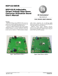
NCP5612GEVB
NCP5612GEVB Evaluation
Board User's Manual
http://onsemi.com
EVAL BOARD USER’S MANUAL
Description
This evaluation board manual contains:
The NCP5612 product is a dual output LED driver
dedicated to the LCD display backlighting. The built-in
DC-DC converter is based on a high efficient charge pump
structure with operating mode 1x and 1.5x.It provides a peak
87% efficiency together with a 0.2% LED to LED matching.
•
•
•
•
Bill of Materials
NCP5612 Demo Board V1.0 schematic diagram
NCP5612 Demo Board V1.0 GERBER views
Manufacturers’ web addresses
Figure 1. NCP5612GEVB Evaluation Board − Details of the Input Power Supply Pins & Digital Control Socket
© Semiconductor Components Industries, LLC, 2012
February, 2012 − Rev. 1
1
Publication Order Number:
EVBUM2016/D
NCP5612GEVB
C1
GND
4.7uF/10V
VBAT
J1
220nF/6.3V
220nF/6.3V
2
1
C2
POWER
TP2
VOUT
C3
S−WIRE PORT
6
CNTL
2
SP1
8
C2 P
9
C2N
10
Vout
Vbat
GND
7
VOUT
2
LED1 D1
3
LED2
C4
1uF/10V
NC
U1
NCP5612
1
TP1
CNTL
5
CNTL
4
3
1
3
5
7
9
C1P
11
J2
2
4
6
8
10
C1 N
12
GND
IREF
LED1
LWY87S
GND
1
LED/ICON
10 k
R1
IREFBK
GND
Z1
GND
GND
Figure 2. NCP5612GEVB Evaluation Board Schematic
http://onsemi.com
2
D2
LWY87S
NCP5612GEVB
Table 1. Bill of Materials
QTY
Designator
1
R1
Footprint
Manufacturer
10 kW
2
Description
0603
Vishay Draloric
C2, C3
220 nF / 10 V
0603
TDK
C1005X5R1C224MT
Reference design
1
C1
4.7 mF / 10 V
0805
TDK
C2012X5R1C475MT
Reference design
1
C4
1 mF / 10 V
0805
TDK
C2012X5R1C105MT
Reference design
1
U1
NCP5612
LLGA12
ON Semiconductor
NCP5612
Reference design
2
D1, D2
LWY87S
OSRAM_LED
OSRAM
LWY87S
Reference design
2
TP1, TP2
Test Point
TEST_POINT
KEYSTONE
5005 ( THM )
RS = 203−4910
Do not assemble
1
J2
IDC10
3M Electronique
2510−6002 UG
RS = 120−7230
ANSLEY
4−1437044−3
RS = 461−742
Control Port
Part Number
Comments
Any other suppliers possible
1
J1
Connector
RAD0.4
KONTEK
COMATEL
3110014000500
RS = 305−0907
(J2 is built with two pins as
depicted in the photo)
1
Z1
GROUND
GND_TEST
HARWIN
D3082−01 (tin)
D3082−05 (gold)
RS = 160−3745 (tin)
1. RS = Radio Spares
2. any resistors with same footprint, tolerance up to ±5% together with TC < 500 ppm and +1055°C operating temperature range can fit the
application.
3. using X5R type ceramic capacitor is preferred. Using X7R brings extended operating temperature range. Using Y5R material shall be
avoided due to the wide tolerance spread over the temperature range. Using smaller foot print capacitor is discouraged to avoid audible noise
issue with the ceramic.
ASSEMBLY
Note: the here attached photos are used as a visual reference:
1. Assemble the NCP5612 ( LLGA12 package) , Hot Air Flow Process mandatory
2. Assemble all the passive parts
3. Assemble all the White LED
4. Assemble the GROUND reference point
5. Assemble the control port IDC10 connector, make sure the connector is properly oriented: the white triangle, on the
PCB, is the pin 1 reference
6. Assemble the power supply pins.
At this point, the system is ready to operate.
http://onsemi.com
3
NCP5612GEVB
TEST CONDITIONS
Power Supply: Connect a DC power supp ly , with 500 mA output current capability, across the two pins built with connector
J2. Make sure the polarity is properly respected: reverse polarity will destroy the NCP5612.
Set up the power polarity to 3.6 V. Although the supply voltage can be adjusted between 2.85 V − 5.5 V for engineering
purpose, the associated MCU test board is limited to 3.6 V: double check the power supply before to turn ON the supply.
Manufacturing Final Test:
1. Connect the IDC10/J1 connector to the external MCU board with the ribbon cable. Double check the power supply is
set up at 3.6 V, maximum rating is 3.8 V.
2. The MCU board is powered by the same external DC supply once the ribbon cable ia attached on both boards.
3. Turn ON the power supply: LED D1 on the MCU board shall turn ON. Reset the MCU if necessary by pushing the
RESET button S7
4. Push control button F3: the ICON mode shall be activated, LED 2 being ON with a low current. At this point, the
current absorbed by the system shall be in the 4 mA range.
5. Push control button F1: the two LED shall be activated and the brightness can be increased by pushing the F1 control.
6. Push control button F2: the two LED shall be dimmed toward zero with consecutive pushes on the F2 command.
7. Push command F3: the ICON mode shall be activated, same as #4
Since bounces are generated by the manual push buttons, non linear operation can happen during the test. This is normal and
the part shall NOT be rejected for such a reason. The final test is complete when all the steps #4 to #7 are proven OK. It is not
necessary to cover all the sixteen steps to ramp up/ down the brightness: the system is fully debugged if the four tests mentioned
above are successful.
Digital Control: it is possible to drive the NCP5612 by means of an external controller, leaving aside the MCU test package.
In this case, one shall connect an external pulse generator to connect J1 /IDC10. The external controller shall send the data
according to the SWIRE protocol depicted into the NCP5612 data sheet. The chip is capable to support a 100 kHz transfer rate.
System Operation:
1. Double check the power supply is set up between 3.0 V to 5.5 V, make sure the external MCU can support the
same power supply range.
2. Turn ON the power supply
3. Send the appropriate data frame to control the two LED
Note: the MCU board is reserved for manufacturing only and is NOT provided with the NCP5612 evaluation board
http://onsemi.com
4
NCP5612GEVB
Figure 3. NCP5612GEVB Evaluation Board & MCU Controller Silk Views
Figure 4. NCP5612GEVB Evaluation Board: TOP & BOTTOM Views
http://onsemi.com
5
NCP5612GEVB
COMPONENT MANUFACTURERS
Vishay − Draloric
TDK
BC Components
http://www.vishay.com/resistors−discrete/
http://www.component.tdk.com/
http://bccomponents.com/
Radio Spares: in the USA, see
ALLIED ELECTRONICS Inc.
7410, Pebble Drive
Forth Worth / Texas / 76118−6997
Phone: 817−595−3500
ON Semiconductor and
are registered trademarks of Semiconductor Components Industries, LLC (SCILLC). SCILLC reserves the right to make changes without further notice
to any products herein. SCILLC makes no warranty, representation or guarantee regarding the suitability of its products for any particular purpose, nor does SCILLC assume any liability
arising out of the application or use of any product or circuit, and specifically disclaims any and all liability, including without limitation special, consequential or incidental damages.
“Typical” parameters which may be provided in SCILLC data sheets and/or specifications can and do vary in different applications and actual performance may vary over time. All
operating parameters, including “Typicals” must be validated for each customer application by customer’s technical experts. SCILLC does not convey any license under its patent rights
nor the rights of others. SCILLC products are not designed, intended, or authorized for use as components in systems intended for surgical implant into the body, or other applications
intended to support or sustain life, or for any other application in which the failure of the SCILLC product could create a situation where personal injury or death may occur. Should
Buyer purchase or use SCILLC products for any such unintended or unauthorized application, Buyer shall indemnify and hold SCILLC and its officers, employees, subsidiaries, affiliates,
and distributors harmless against all claims, costs, damages, and expenses, and reasonable attorney fees arising out of, directly or indirectly, any claim of personal injury or death
associated with such unintended or unauthorized use, even if such claim alleges that SCILLC was negligent regarding the design or manufacture of the part. SCILLC is an Equal
Opportunity/Affirmative Action Employer. This literature is subject to all applicable copyright laws and is not for resale in any manner.
PUBLICATION ORDERING INFORMATION
LITERATURE FULFILLMENT:
Literature Distribution Center for ON Semiconductor
P.O. Box 5163, Denver, Colorado 80217 USA
Phone: 303−675−2175 or 800−344−3860 Toll Free USA/Canada
Fax: 303−675−2176 or 800−344−3867 Toll Free USA/Canada
Email: [email protected]
N. American Technical Support: 800−282−9855 Toll Free
USA/Canada
Europe, Middle East and Africa Technical Support:
Phone: 421 33 790 2910
Japan Customer Focus Center
Phone: 81−3−5817−1050
http://onsemi.com
6
ON Semiconductor Website: www.onsemi.com
Order Literature: http://www.onsemi.com/orderlit
For additional information, please contact your local
Sales Representative
EVBUM2016/D