1
‘
CDB47xxx
Evaluation Kit
CDB47xxx
User ’s Manual
Preliminary Product Information
This document contains information for a new product.
Cirrus Logic reserves the right to modify this product without notice.
Copyright 2009 Cirrus Logic, Inc.
http://www.cirrus.com
SEP 2009
DS886DB4
CDB47xxx User’s Manual
Contacting Cirrus Logic Support
For all product questions and inquiries contact a Cirrus Logic Sales Representative.
To find the one nearest to you go to www.cirrus.com
IMPORTANT NOTICE
“Preliminary” product information describes products that are in production, but for which full characterization data is not yet available.
Cirrus Logic, Inc. and its subsidiaries (“Cirrus”) believe that the information contained in this document is accurate and reliable. However, the information
is subject to change without notice and is provided “AS IS” without warranty of any kind (express or implied). Customers are advised to obtain the latest
version of relevant information to verify, before placing orders, that information being relied on is current and complete. All products are sold subject to the
terms and conditions of sale supplied at the time of order acknowledgment, including those pertaining to warranty, indemnification, and limitation of liability.
No responsibility is assumed by Cirrus for the use of this information, including use of this information as the basis for manufacture or sale of any items, or
for infringement of patents or other rights of third parties. This document is the property of Cirrus and by furnishing this information, Cirrus grants no license,
express or implied under any patents, mask work rights, copyrights, trademarks, trade secrets or other intellectual property rights. Cirrus owns the copyrights associated with the information contained herein and gives consent for copies to be made of the information only for use within your organization
with respect to Cirrus integrated circuits or other products of Cirrus. This consent does not extend to other copying such as copying for general distribution,
advertising or promotional purposes, or for creating any work for resale.
CERTAIN APPLICATIONS USING SEMICONDUCTOR PRODUCTS MAY INVOLVE POTENTIAL RISKS OF DEATH, PERSONAL INJURY, OR SEVERE
PROPERTY OR ENVIRONMENTAL DAMAGE (“CRITICAL APPLICATIONS”). CIRRUS PRODUCTS ARE NOT DESIGNED, AUTHORIZED OR WARRANTED FOR USE IN PRODUCTS SURGICALLY IMPLANTED INTO THE BODY, AUTOMOTIVE SAFETY OR SECURITY DEVICES, LIFE SUPPORT
PRODUCTS OR OTHER CRITICAL APPLICATIONS. INCLUSION OF CIRRUS PRODUCTS IN SUCH APPLICATIONS IS UNDERSTOOD TO BE FULLY
AT THE CUSTOMER'S RISK AND CIRRUS DISCLAIMS AND MAKES NO WARRANTY, EXPRESS, STATUTORY OR IMPLIED, INCLUDING THE IMPLIED WARRANTIES OF MERCHANTABILITY AND FITNESS FOR PARTICULAR PURPOSE, WITH REGARD TO ANY CIRRUS PRODUCT THAT IS
USED IN SUCH A MANNER. IF THE CUSTOMER OR CUSTOMER'S CUSTOMER USES OR PERMITS THE USE OF CIRRUS PRODUCTS IN CRITICAL APPLICATIONS, CUSTOMER AGREES, BY SUCH USE, TO FULLY INDEMNIFY CIRRUS, ITS OFFICERS, DIRECTORS, EMPLOYEES, DISTRIBUTORS AND OTHER AGENTS FROM ANY AND ALL LIABILITY, INCLUDING ATTORNEYS' FEES AND COSTS, THAT MAY RESULT FROM OR ARISE
IN CONNECTION WITH THESE USES.
Cirrus Logic, Cirrus, the Cirrus Logic logo designs, and DSP Composer are trademarks of Cirrus Logic, Inc. All other brand and product names in this document may be trademarks or service marks of their respective owners.
Microsoft, Windows XP are registered trademarks of Microsoft Corporation.
Motorola and SPI are registered trademarks of Motorola, Inc.
I2C is a trademark of Philips Semiconductor Corp.
DS886DB4
Copyright 2009 Cirrus Logic
1-ii
CDB47xxx User’s Manual
Contents
Contents. . . . . . . . . . . . . . . . . . . . . . . . . . . . . . . . . . . . . . . . . . . . . . . . . . . . . . . . . . . . . . . . . . . . . . . . iii
Figures . . . . . . . . . . . . . . . . . . . . . . . . . . . . . . . . . . . . . . . . . . . . . . . . . . . . . . . . . . . . . . . . . . . . . . . . . v
Tables. . . . . . . . . . . . . . . . . . . . . . . . . . . . . . . . . . . . . . . . . . . . . . . . . . . . . . . . . . . . . . . . . . . . . . . . . vii
Chapter 1. Kit Contents and Requirements ........................................................ 1-1
1.1 CDB47xxx Kit Contents . . . . . . . . . . . . . . . . . . . . . . . . . . . . . . . . . . . . . . . . . . . . . . . . . . . . . . .1-1
1.2 Requirements . . . . . . . . . . . . . . . . . . . . . . . . . . . . . . . . . . . . . . . . . . . . . . . . . . . . . . . . . . . . . . .1-3
1.2.1 PC Requirements ...........................................................................................................1-3
1.2.2 Software Requirements ..................................................................................................1-3
1.2.3 Support Hardware Requirements ...................................................................................1-3
1.2.4 Cabling Requirements ....................................................................................................1-3
1.3 CDB47xxx Main Board System Description . . . . . . . . . . . . . . . . . . . . . . . . . . . . . . . . . . . . . .1-4
1.3.1 Audio Inputs....................................................................................................................1-5
1.3.1.1 Analog Line-level Inputs -- Single-Ended (CDB47xxxS only)
(AIN1A - AIN5B, AIN6B) .............................................................................................1-5
1.3.1.2 Analog Line-level Inputs -- Differential (CDB47xxxD only)
(AIN1A - AIN5B, AIN6B) .............................................................................................1-5
1.3.1.3 Optical Digital Input (J21) ..............................................................................1-6
1.3.1.4 Coaxial Digital Input (J4)................................................................................1-6
1.3.1.5 Microphone Input (J9)....................................................................................1-6
1.3.1.6 DSP Digital Audio Input (DAI) (J18 or DAI) ...................................................1-6
1.3.2 Audio Outputs.................................................................................................................1-6
1.3.2.1 Main Analog Line-level Outputs (CDB47xxxS and
CDB47xxxD) (J5-J8, J10-J13, or AOUT_1 - AOUT_8)...............................................1-6
1.3.2.2 Optical Digital Output (J1)..............................................................................1-6
1.3.2.3 Coaxial Digital Output (J35) ...........................................................................1-6
1.3.2.4 DSP Digital Audio Output (DAO) (J24 or DAO) .............................................1-7
1.3.3 DC Power Input (J2) .......................................................................................................1-7
1.3.4 External Control Header (JP1) .......................................................................................1-7
1.3.5 USB Connector (J25) .....................................................................................................1-7
1.3.6 On-Board Voltage Selection Headers (P1-P3) ...............................................................1-7
1.3.7 Digital Audio Input Source Multiplexer (U1)....................................................................1-8
1.3.8 CS470xx Audio System-On-a-Chip (ASOC) ..................................................................1-8
1.3.9 C8051 MCU....................................................................................................................1-9
1.3.10 MCU Input: Push Buttons(S1-S4) and Rotary Encoder (S5)........................................1-9
1.3.11 MCU Output (LCD) (LCD1) ..........................................................................................1-9
1.3.12 Memory (U17, U16 and U14)) ......................................................................................1-9
1.4 CDB47xxx Daughter Card System Description. . . . . . . . . . . . . . . . . . . . . . . . . . . . . . . . . . .1-10
1.4.1 Audio Inputs..................................................................................................................1-12
1.4.1.1 Analog Line-level Inputs (J3) .......................................................................1-12
1.4.1.2 Digital Audio Inputs (DAI) (J2) .....................................................................1-12
1.4.2 Audio Outputs from the CS470xx DSP.........................................................................1-13
1.4.2.1 Analog Line-level Outputs (J3) ....................................................................1-13
1.4.2.2 Digital Audio Outputs (DAO) (J2).................................................................1-13
1.4.3 Control Header (J2) ......................................................................................................1-13
1.4.4 User Input (S1 and S2).................................................................................................1-13
1.4.5 User LED Output (D1and D2).......................................................................................1-13
1.5 Audio Clocking. . . . . . . . . . . . . . . . . . . . . . . . . . . . . . . . . . . . . . . . . . . . . . . . . . . . . . . . . . . . .1-14
1.5.1 Clock and Data Flow for ADC Input..............................................................................1-14
1.5.2 Clock and Data Flow for S/PDIF Input..........................................................................1-15
1.5.3 Clock and Data Flow for DAI Input with Fixed Output Fs .............................................1-16
DS886DB4
Copyright 2009 Cirrus Logic
1-iii
CDB47xxx User’s Manual
1.5.4 Clock and Data Flow for DAI Input with Matched DAO Fs ...........................................1-17
1.6 Other Useful Information. . . . . . . . . . . . . . . . . . . . . . . . . . . . . . . . . . . . . . . . . . . . . . . . . . . . .1-17
1.6.1 Web Sites .....................................................................................................................1-17
1.6.2 DSP Information ...........................................................................................................1-17
1.6.3 Board Information .........................................................................................................1-18
1.6.4 DSP Software Utility Information ..................................................................................1-18
Chapter 2. Introduction to CDB47xxx Kit ............................................................ 2-1
2.1 Introducing the CDB47xxx Customer Development Kit . . . . . . . . . . . . . . . . . . . . . . . . . . . . .2-1
2.2 Identifying CDB47xxx Components . . . . . . . . . . . . . . . . . . . . . . . . . . . . . . . . . . . . . . . . . . . . .2-2
2.2.1 CDB47xxxS Board..........................................................................................................2-2
2.2.1.1 CDB47xxxS Board (Single-Ended) Components ..........................................2-4
2.2.2 CDB47xxxD Board .........................................................................................................2-4
2.2.2.1 CDB47xxxD Board (Differential) Components...............................................2-6
2.2.3 CDB47xxx-DCxx Daughter Card ....................................................................................2-6
2.2.3.1 CDB47xxx-DC48 Daughter Card Components .............................................2-7
Chapter 3. Installation and Setup of Development Board Software ................. 3-1
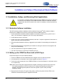
3.1 Installation, Setup, and Running First Application. . . . . . . . . . . . . . . . . . . . . . . . . . . . . . . . .3-1
3.1.1 Evaluation Software Installation .....................................................................................3-1
3.1.2 Setting up the CDB47xxx Board with a DVD Player.......................................................3-1
3.1.3 Connecting to a PC ........................................................................................................3-2
3.1.4 Running a Stereo PCM SPDIF In, DAC Out Application on CDB47xxx .........................3-3
3.1.5 Running a Stereo ADC In, DAC Out Application on CDB47xxx .....................................3-3
Chapter 4. Programming the CDB47xxx Board .................................................. 4-1
4.1 Introduction . . . . . . . . . . . . . . . . . . . . . . . . . . . . . . . . . . . . . . . . . . . . . . . . . . . . . . . . . . . . . . . .4-1
4.2 Running the ADC In / DAC Out Example Application. . . . . . . . . . . . . . . . . . . . . . . . . . . . . . .4-1
4.2.1 System Block..................................................................................................................4-2
4.2.2 Selecting / Changing Audio Input Sources .....................................................................4-3
4.2.2.1 Audio In via ADC ...........................................................................................4-3
4.2.2.2 Audio In via S/PDIF .......................................................................................4-4
4.2.2.3 I2S Audio Input...............................................................................................4-4
4.2.3 Input Channel Remap.....................................................................................................4-4
4.2.4 Output Channel Remap..................................................................................................4-5
4.2.5 Selecting the Audio Output Configuration ......................................................................4-5
4.2.5.1 Audio Out via DAC.........................................................................................4-6
4.2.5.2 Audio Out via S/PDIF Out..............................................................................4-6
4.2.5.3 I2S Audio Input Output...................................................................................4-7
4.2.6 Changing Serial Control Protocol (I2C™ or SPI™) / Flash Type......................................4-7
Chapter 5. Using DSP Composer™ or Micro-Condenser Application
to Create and Load a Flash Image ....................................................................... 5-1
5.1 Programming a Serial Flash Device for Master or Slave Boot Operations . . . . . . . . . . . . .5-1
5.1.1 Using DSP Composer™ to Create and Load a Flash Image for
Master Mode Operations ..........................................................................................................5-1
5.1.2 Using Micro-Condenser to Create and Load a Flash Image for
Slave Mode Operations ............................................................................................................5-3
5.1.2.1 Micro-Condenser Components......................................................................5-3
5.1.2.2 Micro-Condenser Restrictions/ Conventions .................................................5-3
5.1.3 Using Micro-Condenser to Create and Load a Flash Image into the DSP .....................5-4
iv
Copyright 2009 Cirrus Logic, Inc.
DS886DB4
CDB47xxx User’s Manual
5.1.3.1 Creating a Flash Image .................................................................................5-4
5.1.3.2 Programming the Flash Image into the Flash Device ....................................5-4
Chapter 6. CDB47xxx Schematics ....................................................................... 6-1
6.1 Introduction . . . . . . . . . . . . . . . . . . . . . . . . . . . . . . . . . . . . . . . . . . . . . . . . . . . . . . . . . . . . . . . .6-1
6.2 CDB47xxS Single-Ended Schematic Descriptions . . . . . . . . . . . . . . . . . . . . . . . . . . . . . . . . .6-1
6.2.1 CDB47xxxS Block Diagram............................................................................................6-1
6.2.2 Daughterboard Connectors ............................................................................................6-1
6.2.3 Digital Audio and Control Connectors ............................................................................6-1
6.2.4 Memory...........................................................................................................................6-2
6.2.5 Microphone Preamplifier.................................................................................................6-2
6.2.6 Power .............................................................................................................................6-2
6.2.7 Input Filters.....................................................................................................................6-2
6.2.8 Output Filters ..................................................................................................................6-3
6.2.9 MCU Block Diagram .......................................................................................................6-3
6.2.10 MCU .............................................................................................................................6-3
6.2.11 User Interface Devices .................................................................................................6-3
6.3 CDB47xxD Differential Schematic Descriptions . . . . . . . . . . . . . . . . . . . . . . . . . . . . . . . . . .6-16
6.3.1 CDB47xxxD Block Diagram..........................................................................................6-16
6.3.2 Daughterboard Connectors ..........................................................................................6-16
6.3.3 Digital Audio and Control Connectors ..........................................................................6-16
6.3.4 Memory.........................................................................................................................6-16
6.3.5 Microphone Preamplifier...............................................................................................6-16
6.3.6 Power ...........................................................................................................................6-16
6.3.7 Input Filters...................................................................................................................6-16
6.3.8 Output Filters ................................................................................................................6-16
6.3.9 MCU Block Diagram .....................................................................................................6-16
6.3.10 MCU ...........................................................................................................................6-17
6.3.11 User Interface Devices ...............................................................................................6-17
6.4 CDB47xxx-DC48 Daughter Card Schematic . . . . . . . . . . . . . . . . . . . . . . . . . . . . . . . . . . . . .6-30
6.4.1 CDB47xxx-DC48 Block Diagram..................................................................................6-30
6.4.2 CDB47xxx-DC48 Schematic ........................................................................................6-30
6.5 Obtaining Schematic Updates . . . . . . . . . . . . . . . . . . . . . . . . . . . . . . . . . . . . . . . . . . . . . . . .6-33
Chapter 7. Troubleshooting.................................................................................. 7-1
7.1 Troubleshooting Guide . . . . . . . . . . . . . . . . . . . . . . . . . . . . . . . . . . . . . . . . . . . . . . . . . . . . . . .7-1
7.1.1 Power LEDs....................................................................................................................7-1
7.1.2 Board not Recognized by PC .........................................................................................7-1
7.1.3 Audio is not Heard ..........................................................................................................7-2
Revision History . . . . . . . . . . . . . . . . . . . . . . . . . . . . . . . . . . . . . . . . . . . . . . . . . . . . . . . . . . . . . . . .7-2
Figures
Figure 1-1. CDB47xxxS-DCxx Kit Contents .................................................................................................1-2
Figure 1-2. CDB47xxxD-DCxx Kit Contents .................................................................................................1-2
Figure 1-3. CDB47xxxS Main Board Block Diagram ....................................................................................1-4
Figure 1-4. CDB47xxxD Main Board Block Diagram ....................................................................................1-5
DS886DB4
Copyright 2009 Cirrus Logic
1-v
CDB47xxx User’s Manual
Figure 1-5. CDB47xxx-DC48 Daughter Card Block Diagram .....................................................................1-10
Figure 1-6. CDB47xxx-DC28 Daughter Card Block Diagram .....................................................................1-11
Figure 1-7. CDB47xxx-DC24 Daughter Card Block Diagram .....................................................................1-12
Figure 1-8. ADC Clocking ...........................................................................................................................1-14
Figure 1-9. S/PDIF Clocking .......................................................................................................................1-15
Figure 1-10. DAI Clocking with fixed output Fs ..........................................................................................1-16
Figure 1-11. DAI Clocking with fixed output Fs ..........................................................................................1-17
Figure 2-1. CDB47xxx System Block Diagram .............................................................................................2-1
Figure 2-2. CDB47xxxS (Single-ended) Top View .......................................................................................2-3
Figure 2-3. CDB47xxxD Top View (Differential) ...........................................................................................2-5
Figure 2-4. CDB47xxx-DC48 Daughter Card ...............................................................................................2-7
Figure 3-1. CDB47xxx Board with CDB47xxxD (or S)-DC-xx Daughter Card Attached ...............................3-2
Figure 4-1. ADC In / DAC Out Example .......................................................................................................4-2
Figure 4-2. CDB47xxx System Properties ....................................................................................................4-2
Figure 4-3. Selecting Audio In Source using Device Properties Dialog .......................................................4-3
Figure 4-4. ADC2 Device Properties. ...........................................................................................................4-3
Figure 4-5. Selecting ADC2 input Terminals using Device Properties Dialog ..............................................4-4
Figure 4-6. Selecting Multi-Channel I2S Input ..............................................................................................4-4
Figure 4-7. Input Remap Device Properties .................................................................................................4-5
Figure 4-8. Selecting DAC Outputs Only using Device Properties Dialog ...................................................4-6
Figure 4-9. Selecting S/PDIF Outputs and I2S Outputs using Device Properties Dialog .............................4-6
Figure 4-10. Selecting I2S Outputs using Device Properties Dialog ............................................................4-7
Figure 4-11. CDB47xxx Communication Modes / Flash Type .....................................................................4-8
Figure 5-1. Project Properties Dialog Showing the Selection of the I2C
Protocol for Loading the Flash Image ...........................................................................................................5-2
Figure 5-2. Selecting Flash Type via the Advanced Properties Dialog Box .................................................5-2
Figure 6-1. CDB47xxxS (Sngle-ended) Board Block Diagram .....................................................................6-4
Figure 6-2. CDB47xxS (Sngle-ended) Board Schematic Index ...................................................................6-5
Figure 6-3. CDB47xxxS (Sngle-ended) Daughter Card Connectors ............................................................6-6
Figure 6-4. CDB47xxxS (Sngle-ended) Digital Audio Control Connectors ...................................................6-7
Figure 6-5. CDB47xxxS (Sngle-ended) Serial Memory ................................................................................6-8
Figure 6-6. CDB47xxxS (Sngle-ended) Mic Pre-Amp ..................................................................................6-9
Figure 6-7. CDB47xxxS (Sngle-ended) Power Connectors .......................................................................6-10
Figure 6-8. CDB47xxxS (Sngle-ended) ADC Filters ..................................................................................6-11
Figure 6-9. CDB47xxxS (Sngle-ended) DAC Filters ..................................................................................6-12
Figure 6-10. CDB47xxxS (Sngle-ended) Microcontroller Card Interface ...................................................6-13
Figure 6-11. CDB47xxxS (Sngle-ended) Microcontroller Card User Interface ...........................................6-14
vi
Copyright 2009 Cirrus Logic, Inc.
DS886DB4
CDB47xxx User’s Manual
Figure 6-12. CDB47xxxS (Sngle-ended) Microcontroller Card User Interface ...........................................6-15
Figure 6-13. CDB47xxD (Differential) Board Block Diagram ......................................................................6-18
Figure 6-14. CDB47xxD (Differential) Board Schematic Index ..................................................................6-19
Figure 6-15. CDB47xxD (Differential)Daughter Card Connectors ..............................................................6-20
Figure 6-16. CDB47xxD (Differential) Digital Audio Control Connectors ....................................................6-21
Figure 6-17. CDB47xxD (Differential) Digital Serial Flash ..........................................................................6-22
Figure 6-18. CDB47xxD (Differential) Mic Pre-Amp ...................................................................................6-23
Figure 6-19. CDB47xxxD (Differential) Power Connectors ........................................................................6-24
Figure 6-20. CDB47xxD (Differential) ADC Filters .....................................................................................6-25
Figure 6-21. CDB47xxD (Differential) Voltage Output Circuitry .................................................................6-26
Figure 6-22. CDB47xxD (Differential) Microcontroller Card Interface ........................................................6-27
Figure 6-23. CDB47xxD (Differential) Microcontroller Card Schematic ......................................................6-28
Figure 6-24. CDB47xxD (Differential) Microcontroller Card User Interface ................................................6-29
Figure 6-25. CDB47xxx-DC48 Daughter Card Block Diagram ...................................................................6-31
Figure 6-26. CDB47xxx-DC48 Daughter Card Schematic .........................................................................6-32
Tables
Table 1-1. CDB47xxx Kit Contents................................................................................................................1-1
DS886DB4
Copyright 2009 Cirrus Logic
1-vii
CDB47xxx User’s Manual
viii
Copyright 2009 Cirrus Logic, Inc.
DS886DB4
CDB47xxx Kit Contents
CDB47xxx User’s Manual
Chapter 1
Kit Contents and Requirements
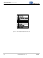
1.1 CDB47xxx Kit Contents
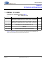
Each CDB47xxx kit comes with the items listed in Table 1-1.
Table 1-1. CDB47xxx Kit Contents
CRD Kit
Item
Quantity
CDB47xxxS-DC48
CDB47xxxS-DC28
CDB47xxxS-DC24
CDB47xxxS Single-Ended Development Board with integrated MCU & USB interface
with Daughter Card populated with either the CS47048, CS4028, or CS47024 DSP.
1
CDB47xxxD-DC48
CDB47xxxD-DC28
CDB47xxxD-DC24
CDB47xxxD Differential Development Board with integrated MCU & USB interface
with Daughter Card populated with either the CS47048, CS4028, or CS47024 DSP.
1
CDB47xxxS-DCxx
CDB47xxxD-DCxx
Power Supply: +9V, 2A, 100V - 240V with AC Power Cord
1
CDB47xxxS-DCxx
CDB47xxxD-DCxx
USB Cable
1
CDB47xxxS-DCxx
CDB47xxxD-DCxx
Document Card explaining how to get the latest board software
1
Figure 1-1 and Figure 1-2 show the kit contents for the CDB47xxxS-DCxx (Single-ended) and
CDB47xxxD-DCxx (Differential) development boards respectively.
DS886DB4
Copyright 2009 Cirrus Logic, Inc
1-1
CDB47xxx Kit Contents
CDB47xxx User’s Manual
Figure 1-1. CDB47xxxS-DCxx Kit Contents
Figure 1-2. CDB47xxxD-DCxx Kit Contents
DS886DB4
Copyright 2009 Cirrus Logic, Inc
1-2
Requirements
CDB47xxx User’s Manual
1.2 Requirements
1.2.1 PC Requirements
•
Microsoft® Windows XP® Operating System with Service Pack 2 or higher.
•
USB 2.0 Support
1.2.2 Software Requirements
•
Cirrus® Evaluation Software Package (available from your local Cirrus Logic representative)
1.2.3 Support Hardware Requirements
•
Digital or Analog Audio Source (for example, DVD player, PC with a digital audio card/device)
•
Amplified Speakers for audio playback (for example, powered PC speakers, AVR/amp + speakers)
1.2.4 Cabling Requirements
1-3
•
Digital Audio Inputs – S/PDIF optical cables, RCA audio cables (Connect to digital audio card, audio
analyzer, or DVD player.)
•
Digital Audio Output – S/PDIF Optical cable, RCA audio cable (Connect to digital audio card, audio
analyzer, or AVR.)
•
Analog Audio Inputs – 1/8” stereo plug microphone cable (Connect microphone to ADC), RCA audio
cables (CDB47xxxS only), 1/8” stereo plug differential cable (CDB47xxxD only)
•
Analog Audio Outputs – RCA audio cables (Connect CDB47xxx line-level outputs to powered
speakers.)
Copyright 2009 Cirrus Logic, Inc.
DS886DB4
CDB47xxx Main Board System Description
CDB47xxx User’s Manual
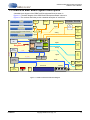
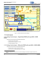
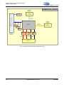
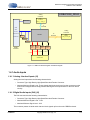
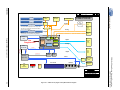
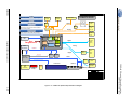
1.3 CDB47xxx Main Board System Description
A detailed block diagram of the CDB47xxxS Development Board is shown in
Figure 1-3. The block diagram of the CDB47xxxD Development Board is shown in
Figure 1-4 The sections that follow provide a detailed description of each block.
SPDIF - IN
COAX
I2S HDRs
SPDIF - IN
OPTICAL
Header will be available to probe / bring in I2S signals
CDB47XXXS
I2S IN HDR
20 Pin HDR
Standard 20 Pin Debug Header (Serial Control & Debug)
Buffer
Mic
Pre-Amp
Circuitry
Digital
DSP Daughtercard
Mic Input
Jack
The Chronos DSP Daughercard will have only the DSP.
This allows us to easily swap out the DSP for different
CS47xxx Family members.
Analog
Digital
DAO Buttons/LEDs
RCA
IN
2 ch (x4)
RCA IN
2ch
DAO pins on Chronos are also GPIO. These buttons/LEDs
Can be used by the new primitives being developed
GPIO
HDR
GPIO
Use
DaughterCard
SRC
SPDIF
Rx
I2S in
(8 ch)
CS47xxx
DSP CORE
I2S out
(8 ch)
DAC
Digital
I2S OUT
HDR
(8 ch)
Analog
Control
Control
EXT CTRL
SEL
ADC
SPDIF Tx
Control
SMALL
20-PIN HDR
5:1
mux
ADC
8ch
RCA
OUT
Digital
SPI
FLASH
SPI_HOLD
I2C
FLASH
USB MCU
Silicon Labs
GPIO
Control (Parallel Port)
Buffer
LCD Panel
USB
(DSP
Composer)
Power In
Wall Adapter
SPDIF - OUT
OPTICAL
Buttons
Power
LEDs
B1
B2
B3
SPDIF - OUT
COAX
B4
Rotary Knob
Figure 1-3. CDB47xxxS Main Board Block Diagram
DS886DB4
Copyright 2009 Cirrus Logic, Inc
1-4
CDB47xxx Main Board System Description
CDB47xxx User’s Manual
CDB47XXXD
I2S HDRs
SPDIF - IN
COAX
Header will be available to probe / bring in I2S signals
SPDIF - IN
OPTICAL
I2S IN HDR
20 Pin HDR
Standard 20 Pin Debug Header (Serial Control & Debug)
Mic
Pre-Amp
Circuitry
Digital
Buffer
DSP Daughtercard
The Chronos DSP Daughercard will have only the DSP.
Diff
Amp
This allows us to easily swap out the DSP for different
CS47xxx Family members.
DAO Buttons/LEDs
Stereo 1/8"
IN
2 ch (x4)
Analog
Digital
DAO pins on Chronos are also GPIO. These buttons/LEDs
Can be used by the new primitives being developed
GPIO
HDR
Stereo 1/8"
IN
2ch
GPIO
Use
DaughterCard
SPDIF
Rx
5:1
mux
ADC
I2S in
(8 ch)
Digital
I2S OUT
HDR
(8 ch)
DAC
DSP CORE
SPDIF Tx
Analog
Control
Control
EXT CTRL
SEL
ADC
I2S out
(8 ch)
CS47xxx
SRC
Control
SMALL
20-PIN HDR
SPI
FLASH
8ch
RCA
OUT
Diff
Amp
Digital
SPI_HOLD
I2C
FLASH
USB MCU
Silicon Labs
GPIO
Control (Parallel Port)
Buffer
Buttons
LCD Panel
USB
(DSP
Composer)
Mic Input
Jack
Power In
SPDIF - OUT
OPTICAL
Power
LEDs
B1
Wall Adapter
B2
B3
SPDIF - OUT
COAX
B4
Rotary Knob
Figure 1-4. CDB47xxxD Main Board Block Diagram
1.3.1 Audio Inputs
1.3.1.1 Analog Line-level Inputs -- Single-Ended (CDB47xxxS only) (AIN1A - AIN5B,
AIN6B)1
Analog line-level inputs have the following characteristics:
•
Connector Type: RCA Female
•
Absolute Maximum Signal Level: 8Vp-p
•
Full Scale Amplitude: 2VRMS
1.3.1.2 Analog Line-level Inputs -- Differential (CDB47xxxD only) (AIN1A - AIN5B, AIN6B)
Analog line-level inputs have the following characteristics:
•
Connector Type: 3.5mm (1/8”) Stereo Female
•
Absolute Maximum Differential Signal Level: 16Vp-p
1. Reference designators are listed at the end of the heading for each board component listed in this
chapter.
1-5
Copyright 2009 Cirrus Logic, Inc.
DS886DB4
CDB47xxx Main Board System Description
CDB47xxx User’s Manual
•
Full Scale Differential Amplitude: 4VRMS
1.3.1.3 Optical Digital Input (J21)
Optical digital inputs have the following characteristics:
•
Connector Type: Fiber Optic RX for Digital Audio, JIS F05 (TOSLINK)
1.3.1.4 Coaxial Digital Input (J4)
Coaxial digital inputs have the following characteristics:
•
Connector Type: RCA Female
•
Input Impedance: 75Ω
•
Maximum Signal Level: 1.5Vp-p
1.3.1.5 Microphone Input (J9)
The microphone input has a stereo connector, but only the LEFT channel is used for the microphone
input. This input has the following characteristics:
•
Connector Type: 3.5mm (1/8”) Stereo Female
•
Absolute Maximum Signal Level: 8Vp-p
•
Full Scale Amplitude: 20mVp-p
1.3.1.6 DSP Digital Audio Input (DAI) (J18 or DAI)
The DAI connector has the following characteristics:
•
Connector Type: 2x10, 0.100 inch Male Header
•
Absolute Maximum Signal Level: +3.6V
•
Absolute Minimum Signal Level: -0.3V
1.3.2 Audio Outputs
1.3.2.1 Main Analog Line-level Outputs (CDB47xxxS and CDB47xxxD) (J5-J8, J10-J13, or
AOUT_1 - AOUT_8)
Analog line-level outputs are RCA connectors on both the single-ended and differential boards. The
CDB47xxxD board has a differential to single-ended amplifier that feeds the RCA connectors. The outputs
have the following characteristics:
•
Connector Type: RCA Female
•
Full Scale Amplitude: 2VRMS
1.3.2.2 Optical Digital Output (J1)
The optical digital output has the following characteristics:
•
Connector Type: Fiber Optic TX for Digital Audio, JIS F05 (TOSLINK)
1.3.2.3 Coaxial Digital Output (J35)
The coaxial digital output has the following characteristics:
DS886DB4
•
Connector Type: RCA Female
•
Maximum Signal Output Level: 1Vp-p into 75Ω load
Copyright 2009 Cirrus Logic, Inc
1-6
CDB47xxx Main Board System Description
CDB47xxx User’s Manual
1.3.2.4 DSP Digital Audio Output (DAO) (J24 or DAO)
The DAO connector has the following characteristics:
•
Connector Type: 2x10, 0.100 inch Male Header
•
Absolute Maximum Signal Level: +3.6V
•
Absolute Minimum Signal Level: -0.3V
1.3.3 DC Power Input (J2)
The DC power input has the following characteristics:
•
Voltage Range: +9VDC TO +12VDC
•
Minimum Power: 18W supply (2A @ 9V)
•
Connector Type: 2mm female barrel connector with a positive center pin
1.3.4 External Control Header (JP1)
The control header has the following characteristics:
•
Connector Type: 2x10, 0.100 inch Shrouded Male
•
Absolute Maximum Signal Level: +3.6V
•
Absolute Minimum Signal Level: -0.3V
This connector is the interface between the CS470xx DSP and an external host. This connector is used to
control the DSP when the on-board MCU is bypassed.
1.3.5 USB Connector (J25)
The control header has the following characteristics:
•
Connector Type: USB Connector
•
Absolute Maximum Signal Level: +5V
•
Absolute Minimum Signal Level: -0.3V
1.3.6 On-Board Voltage Selection Headers (P1-P3)
The on-board voltage selection headers have the following characteristics:
•
Connector Type: 1x2, 0.100 inch, Stake Header
The CDB47xxx is designed to operate from a single DC power input. The 9V power supply provided with
the kit is connected to the DC power input jack (J22) and is regulated down to the system voltages (5V,
3.3V, 1.8V). The power selection headers should be installed when using the DC wall supply. This is the
default mode of operation and should not need to be changed for most applications.
It is possible to bypass the regulated power supplies for any of the voltages by removing the jumper from
the appropriate power selection header, and connecting an external voltage supply to pin 2 of that
selection header. Pin 1 of each header is marked with a triangle and the word “REG”. Pin 2 of each
header is labeled with the voltage required for that pin (+5V, +3.3V, or +1.8V).
1-7
Copyright 2009 Cirrus Logic, Inc.
DS886DB4
CDB47xxx Main Board System Description
CDB47xxx User’s Manual
1.3.7 Digital Audio Input Source Multiplexer (U1)
The audio input source multiplexer has the following characteristics:
•
Source 1: Optical S/PDIF Input
•
Source 2: Coaxial S/PDIF Input
•
Source 3: Digital Audio Input (DAI) Header
This multiplexer is used to select which audio source feeds the CS470xx DAI3 pin. When the CS470xx
has DAI3 configured as a S/PDIF receiver, either Source 1 or Source 2 can be selected by the MCU.
When DAI3 is configured as a standard I2S input, Source 3 can be selected as the data source.
The CDB47xxx has been designed to indicate which input is currently selected by illuminating a specific
LED for each Source, as described below:
•
Source 1 selected: D12 will be on
•
Source 2 selected: D51 will be on
•
Source 3 selected: D5 will be on
1.3.8 CS470xx Audio System-On-a-Chip (ASOC)
The CS470xx ASOCs are a family of ICs designed specifically for audio applications. The CDB47xxx
allows a designer to evaluate the CS470xx ASOCs in many different modes of multi-channel input and
output. The 100-pin footprint on the daughtercard is compatible with any CS470xx chip that uses the
LQFP100 package.
Audio input data to the ASOC can come from any of the following sources:
•
Line-Level Analog Audio Input Connectors
•
Optical S/PDIF Input Connector
•
Coaxial S/PDIF Input Connector
•
DAI Header
Audio output data from the ASOC can be sent to the following destinations:
•
Line-Level Analog Audio Output Connectors
•
Optical S/PDIF Output Connector
•
Coaxial S/PDIF Input Connector
•
DAO Header
The CS470xx can be booted from external serial Flash for custom applications in which a host MCU is not
desired.
The CDB47xxx also allows the PC to act as a host to boot and configure the DSP through the GUI
software for real-time configuration of the audio processing.
DS886DB4
Copyright 2009 Cirrus Logic, Inc
1-8
CDB47xxx Main Board System Description
CDB47xxx User’s Manual
1.3.9 C8051 MCU
The C8051 (U15) is a USB slave controller and general purpose MCU used to control the CDB47xxx
Board in stand-alone applications, and also used to interface to the PC through the USB port (DSP
Composer). Standalone applications can be as simple as using the MCU to configure the inputs on the
board to feed the DSP and provide a power-on-reset (POR) to the DSP. But standalone applications can
also take advantage of the LCD display, buttons, and rotary encoder to provide a user interface that is
managed by the C8051.
When DSP Composer is needed to perform real-time application development on the CS470xx, the USB
port should be used to connect the CDB47xxx Board to a PC that has DSP Composer™ installed.
1.3.10 MCU Input: Push Buttons(S1-S4) and Rotary Encoder (S5)
The C8051 can accept user input through the buttons on the CDB47xxx when USB is not connected.
There are 4 momentary contact push-buttons provided:
There is also a rotary encoder knob that can be used to scroll up and down through options provided
through the MCU interface. The rotary encoder has an integrated momentary contact push-button that is
activated by pushing down on the knob:
1.3.11 MCU Output (LCD) (LCD1)
The C8051 can provide feedback to the user through the on-board LCD when USB is not connected:
1.3.12 Memory (U17, U16 and U14))
The CDB47xxx is assembled with a 32-Mbit SPI Flash (U17) and a 512-kbit I2C Flash (U16) which are
dedicated for DSP firmware and configuration data. The serial control lines are routed down from the DSP
through the daughter-card connectors.
There is an additional 32-Mbit SPI Flash component on the board (U14) that is used only to store MCU
firmware, and it is not required by the DSP.
1-9
Copyright 2009 Cirrus Logic, Inc.
DS886DB4
CDB47xxx Daughter Card System Description
CDB47xxx User’s Manual
1.4 CDB47xxx Daughter Card System Description
The CS470xx Audio SOC Daughter card is exactly the same for both the CDB47xxxS and CDB47xxxD
evaluation kits. All of the analog and digital audio signals are fed to the CS470xx (U1) through the
daughter board connectors (J2 - J3). All of the analog pins of the CS470xx are connected to the analog
daughterboard connector (J3). The distinction between a differential system and single-ended system is
made on the main board where either the full differential pair is used, or only the positive (+) half of the
pair.
A detailed block diagram of the CDB47xxxD(or S)-DC48 daughter card for single-ended or differential
platforms is shown in Figure 1-5. The CDB47xxxD ( or S)-DC28 and CDB47xxxD (or S)-DC24 daughter
cards for single-ended or differential platforms are shown in Figure 1-6 and Figure 1-7 respectively. The
sections that follow provide a detailed description of each block.
CDB47XXX_DC48
Analog
Connector
DAC
OUTPUTS
AOUT_1 – AOUT_8
DC_ID
SHIFT REG
8
GPIO
I2S In
I2S Out
Analog
Connector
Serial Control
S/PDIF In
S/PDIF Out
CS47048
LED x 2
12
ADC
INPUTS
AIN_1A – AIN_6B
SWITCH
BUTTON
Digital
Connector
Current
Measure
Point
+3.3VD
Current
Measure
Point
Current
Measure
Point
+1.8VD +3.3VA
Current
Measure
Point
+1.8VA
POWER
CONNECTOR
Figure 1-5. CDB47xxx-DC48 Daughter Card Block Diagram
DS886DB4
Copyright 2009 Cirrus Logic, Inc
1-10
CDB47xxx Daughter Card System Description
CDB47xxx User’s Manual
CDB47XXX_DC28
Analog
Connector
DAC
OUTPUTS
AOUT_1 – AOUT_8
DC_ID
SHIFT REG
8
Channels
GPIO
I2S In
I2S Out
Analog
Connector
Serial Control
S/PDIF In
S/PDIF Out
10
Channels
CS47028
LED x 2
ADC
INPUTS
AIN_2A – AIN_6B
SWITCH
BUTTON
Digital
Connector
Current
Measure
Point
+3.3VD
Current
Measure
Point
Current
Measure
Point
+1.8VD +3.3VA
Current
Measure
Point
+1.8VA
POWER
CONNECTOR
Figure 1-6. CDB47xxx-DC28 Daughter Card Block Diagram
1-11
Copyright 2009 Cirrus Logic, Inc.
DS886DB4
CDB47xxx Daughter Card System Description
CDB47xxx User’s Manual
CDB47XXX_DC24
Analog
Connector
DAC
OUTPUTS
AOUT_1 – AOUT_4
DC_ID
SHIFT REG
4
Channels
GPIO
I2S In
Analog
Connector
I2S Out
Serial Control
S/PDIF Out
10
Channels
CS47024
LED x 2
ADC
INPUTS
AIN_2A – AIN_6B
SWITCH
BUTTON
Digital
Connector
Current
Measure
Point
+3.3VD
Current
Measure
Point
Current
Measure
Point
+1.8VD +3.3VA
Current
Measure
Point
+1.8VA
POWER
CONNECTOR
Figure 1-7. CDB47xxx-DC24 Daughter Card Block Diagram
1.4.1 Audio Inputs
1.4.1.1 Analog Line-level Inputs (J3)
Analog line-level inputs have the following characteristics:
•
Connector Type: High-Density High-Speed Shrouded Female Connector
•
Absolute Maximum Signal Level: These signals should only be driven from the connectors on the
main board. Voltages should comply with the Max Signal Level specification for the main board
circuitry.
1.4.1.2 Digital Audio Inputs (DAI) (J2)
The DAI connector has the following characteristics:
•
Connector Type: High-Density High-Speed Shrouded Female Connector
•
Absolute Maximum Signal Level: +3.6V
•
Absolute Minimum Signal Level: -0.3V
This connector passes all serial audio data and clock signals up from the main CDB47xxx board.
DS886DB4
Copyright 2009 Cirrus Logic, Inc
1-12
CDB47xxx Daughter Card System Description
CDB47xxx User’s Manual
1.4.2 Audio Outputs from the CS470xx DSP
1.4.2.1 Analog Line-level Outputs (J3)
Analog line-level outputs have the following characteristics:
•
Connector Type: High-Density High-Speed Shrouded Female Connector
•
Maximum Signal Output Level: These signals should only be driven from the connectors on the main
board. Voltages will comply with the Max Signal Level specification for the main board circuitry.
1.4.2.2 Digital Audio Outputs (DAO) (J2)
The DAO connector has the following characteristics:
•
Connector Type: High-Density High-Speed Shrouded Female Connector
•
Absolute Maximum Signal Level: +3.6V
•
Absolute Minimum Signal Level: -0.3V
This connector passes all serial audio data and clock signals up from the main CS47xxx board.
1.4.3 Control Header (J2)
The control header has the following characteristics:
•
Connector Type: High-Density High-Speed Shrouded Female Connector
•
Absolute Maximum Signal Level: +3.6V
•
Absolute Minimum Signal Level: -0.3V
This connector passes all serial control signals up from the main CS47xxx board.
1.4.4 User Input (S1 and S2)
The CS470xx can be configured to accept user input through the slide switch and button on the
daughtercard. The button and switch are connected to GPIO pins on the ASOC which are monitored by
the DSP. This feature is firmware dependent and may not be available in all applications.
There is a slide switch (S1) provided. It can connect Pin 7 (GPIO0) of the DSP to either 3.3V or ground
through a 10K resistor on the DSP.
There is a momentary contact push-button (S2) provided. When pressed it connects Pin 19 (GPIO3) to
3.3V through a pull-up resistor.
1.4.5 User LED Output (D1and D2)
The CS470xx can be configured to provide user feedback through LEDs on the daughtercard. This
feature is firmware dependent and will not be available in all applications.
There are 2 LEDs provided for user feedback. These LEDs light up when their associated GPIO pin is
driven low by the DSP. The LEDs map to their pins as follows:
1-13
•
LED D1 is connected to pin 7 (GPIO16) of the DSP.
•
LED D2 is connected to pin 15 (GPIO6) of the DSP.
Copyright 2009 Cirrus Logic, Inc.
DS886DB4
Audio Clocking
CDB47xxx User’s Manual
1.5 Audio Clocking
Clocking architecture is one of the most important aspects of an audio system. This can also be one of the
most complicated parts of a system design to insure that clocking is valid and stable for all scenarios. This
is one of the major advantages of the CS470xx Audio System On-a-Chip (ASOC). Because of the
integrated ADC and DAC along with the integrated SRCs, The CS470xx makes audio clocking very
simple. For analog-only systems, the clocking architecture is as simple as a crystal feeding the CS470xx.
Traditionally the input and output clock domains of the DSP needed to be synchronous when delivering
audio data in an isochronous fashion (constant bitrate delivery), even if the input/output domains operate
at different frequencies (e.g. 48 kHz input/96 kHz output). Systems utilizing serial audio data (I2S) delivery
would thus use isochronous delivery.
The CS470xx’s integrated SRCs remove this requirement because the CS470xx can rate match the input
(DAI) Fs to any Fs on the output side (DAO). The examples below show configurations that support an Fs
that is synchronized between DAI and DAO, as well as an output Fs that is independent of the input Fs.
1.5.1 Clock and Data Flow for ADC Input
CS470xx
DAO
(I2S)
DAI
(I2S)
Line-Level Analog
Line-Level Analog
ADC
DAC
Line-Level Analog
Input Connectors
Line-Level Analog
Output Connectors
Figure 1-8. ADC Clocking
The ADC clocking architecture is used when the internal ADCs are used as the only audio input (that is, S/
PDIF is disabled and there are no serial audio signals connected to DAI or DAO). In this scenario, the
CS470xx has all audio clocking self contained. Figure 1-8 illustrates this clocking configuration.
The clock fed to XTI of the CS470xx is MCLK for the system, and the ASOC masters clocks to DAC and
ADC. The user need only route in analog signals and route out the processed analog signals.
DS886DB4
Copyright 2009 Cirrus Logic, Inc
1-14
Audio Clocking
CDB47xxx User’s Manual
1.5.2 Clock and Data Flow for S/PDIF Input
I2S Clocks
and Data
CS470xx
S/PDIF Input
Connector
DAI
(I2S)
S/PDIF
RX
DAO Header
SRC
DAO
(I2S)
Line-Level Analog
ADC
DAC
Line-Level Analog
Output Connectors
Figure 1-9. S/PDIF Clocking
The S/PDIF clocking architecture is used when any S/PDIF RX is used as an audio source, whether from
the optical RX, coaxial RX, or brought in on the DAI header. Figure 1-9 illustrates this clocking
configuration.
The incoming S/PDIF stream is always rate matched to another MCLK in the system through an SRC.
This means that the DAO can be run at a constant Fs that is independent of the incoming S/PDIF Fs. This
is useful in systems with digital amplifiers and wireless audio transmitter modules that requires a fixed Fs.
The CS470xx can master its output clocks, or slave to clocks from another source.
1-15
Copyright 2009 Cirrus Logic, Inc.
DS886DB4
Audio Clocking
CDB47xxx User’s Manual
1.5.3 Clock and Data Flow for DAI Input with Fixed Output Fs
I2S Clocks
and Data
I2S Clocks
and Data
CS470xx
DAI Header
DAI
(I2S)
DAO Header
SRC
DAO
(I2S)
Line-Level Analog
ADC
DAC
Line-Level Analog
Output Connectors
Figure 1-10. DAI Clocking with fixed output Fs
The DAI clocking architecture is used when any serial audio data source is connected to the DAI header.
Figure 1-10 illustrates this clocking configuration. Note that the incoming DAI data is passed out of the
CS470xx at the Fs of the crystal connected to the ASOC.
Like the S/PDIF clocking configuration, this allows the DAI to be rate matched to another MCLK in the
system through an SRC. This means that the DAO can be run at a constant Fs that is independent of the
incoming DAI Fs. This is useful in systems with a digital amplifier that requires a fixed Fs.
The CS470xx can masters its output clocks, or slave to clocks from another source
DS886DB4
Copyright 2009 Cirrus Logic, Inc
1-16
Other Useful Information
CDB47xxx User’s Manual
1.5.4 Clock and Data Flow for DAI Input with Matched DAO Fs
MCLK
I2 S Clocks
and Data
I2 S Clocks
and Data
CS470xx
DAI
(I2 S)
DAO Header
DAO
(I2 S)
DAI Header
Line-Level Analog
ADC
DAC
Line-Level Analog
Output Connectors
Figure 1-11. DAI Clocking with fixed output Fs
The DAI clocking architecture is used when any serial audio data source is connected to the DAI header.
Figure 1-11 illustrates this clocking configuration. Note that the incoming DAI data is synchronized to the
DAO using a common MCLK.
This is a more traditional clocking architecture for serial audio data, where the DAI Fs and the DAO Fs are
synchronous. In this configuration, the SRC is bypassed for the DAO.
1.6 Other Useful Information
1.6.1 Web Sites
•
Cirrus Logic main web site: www.cirrus.com
1.6.2 DSP Information
The following information can be obtained from your Cirrus Logic representative.
1-17
•
CS470xx Data Sheet
•
CS470xx Hardware User’s Manual
•
AN333, CS470xx Firmware User’s Manual
Copyright 2009 Cirrus Logic, Inc.
DS886DB4
Other Useful Information
CDB47xxx User’s Manual
1.6.3 Board Information
•
The following information can be obtained from your local Cirrus Logic representative.
•
Schematics
•
BOM
•
Artwork and PCB stackup
1.6.4 DSP Software Utility Information
The following information can be obtained from your local Cirrus representative.
•
DSP Composer™ User’s Manual
•
DSP Composer™ Primitive Elements Reference
The documents listed above are updated periodically and may be more up-to-date than the information in
this document. Contact your Cirrus Logic sales representative for the latest updates.
§§2
2. The “§§” symbol is used throughout this manual to indicate the end of the text flow in a chapter.
DS886DB4
Copyright 2009 Cirrus Logic, Inc
1-18
Introducing the CDB47xxx Customer Development Kit
CDB47xxx User’s Manual
Chapter 2
Introduction to CDB47xxx Kit
2.1 Introducing the CDB47xxx Customer Development Kit
The CDB47xxx kit is composed of the CDB47xxxS or CDB47xxxD main board and a daughtercard that
can support any member of the CS470xx Audio SOC (ASOC) family. The CDB47xxx provides a practical
platform for emulating a typical multi-channel audio system application. The system can be an
independent evaluation platform controlled by the on-board MCU, or using the USB connector, the CDB
can be connected to a host PC which can configure and control the board using DSP Composer, the
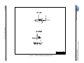
Cirrus Proprietary GUI. Figure 2-1 shows the relationship between the CDB47xxx and the optional PC.
OPTIONAL
PC
USB Port
CDB47xxx
Figure 2-1. CDB47xxx System Block Diagram
This document will concentrate on the features and basic operation of the CDB47xxx kit. Detailed
information regarding the operation and programming of the CS470xx Audio SOC is covered by the
CS470xx Data Sheet, CS470xx Hardware User’s Manual and application note AN333 See Section 1.6
“Other Useful Information” on page 17 for more details.
The CDB47xxx is a convenient and easy-to-operate evaluation platform. It has been designed to
demonstrate the majority of the CS470xx functions on a small base board. These features include:
2-1
•
PC control of the CS470xx using the DSP Composer™ graphical user interface
•
Serial control of audio devices on CDB47xxx via I2C™ or SPI™ protocols
•
Digital audio input of PCM or compressed data via optical or coaxial S/PDIF
•
Up to 4-channels of simultaneous analog audio input via the integrated ADCs of the CS470xx
•
The 5:1 analog multiplexer integrated into one of the CS470xx ADCs
•
Up to 8-channel analog output via the integrated DACs of the CS470xx
•
Digital audio output of PCM data via optical or coaxial S/PDIF
•
Multi-channel digital audio input via the DAI serial audio (I2S) header
•
Capability to support fixed output Fs that is independent of input Fs
Copyright 2009 Cirrus Logic, Inc.
DS886DB4
Identifying CDB47xxx Components
CDB47xxx User’s Manual
•
Fast boot – master boot of custom applications from 32 Mbit serial SPI Flash device or 512 kbit I2C
device.
•
Microphone input with integrated amplifier
•
Supports all members of the CS470xx family in the 100-pin LQFP package.
Note: Not all features of the CS470xx are exercised on the CDB47xxx.
2.2 Identifying CDB47xxx Components
2.2.1 CDB47xxxS Board
Figure 2-2 shows the top side of the CDB47xxxS Board. Section 2.2.1.1 contains the legend for the
reference points called out in red in Figure 2-2.CDB47xxxS Top View (Single-ended)
DS886DB4
Copyright 2009 Cirrus Logic, Inc
2-2
DS886DB4
.
10
24
23
21
Copyright 2009 Cirrus Logic, Inc
22
18
Identifying CDB47xxx Components
CDB47xxx User’s Manual
2-3
Figure 2-2. CDB47xxxS (Single-ended) Top View
11
12
13
14
15
16
17
8
7
6
5
4
3
2
1
9
26
25
20
19
Identifying CDB47xxx Components
CDB47xxx User’s Manual
2.2.1.1 CDB47xxxS Board (Single-Ended) Components
The circled numbers found in Figure 2-2 refer to the CDB47xxxS board (single-ended) components in the
following list.
1. +9V Power In
2. Optical S/PDIF Out
3. Coax S/PDIF Out
4. Optical S/PDIF In
5. Coax S/PDIF In
6. +5V Header
7. Line-Level Analog Outputs
8. CDB47xxS-DC48 Daughter Card Connectors
9. Mac Input
10. Single-Ended Line-Level Inputs
11. MCU Rotary Encoder
12. MCU Buttons
13. SPI Flash
14. I2C EEPROM
15. LCD
16. DSP DAO Header
17. IR Receiver
18. Board Reset
19. MCU Programming Header
20. MCU Control Bypass Header
21. USB Connector
22. DSP External Control Header
23. DSP DAI Header
24. +1.8V Header
25. Power LEDs (4)
26. + 3.3V Header
2.2.2 CDB47xxxD Board
Figure 2-3 shows the top side of the CDB47xxxD Board. Section 2.2.2.1 contains the legend for the
reference points called out in red in Figure 2-3.
DS886DB4
Copyright 2009 Cirrus Logic, Inc
2-4
DS886DB4
.
10
23
21
20
Copyright 2009 Cirrus Logic, Inc
22
18
Identifying CDB47xxx Components
CDB47xxx User’s Manual
2-5
Figure 2-3. CDB47xxxD (Differential) Top View
11
12
13
14
15
16
17
8
7
6
5
4
3
2
1
9
26
25
24
19
Identifying CDB47xxx Components
CDB47xxx User’s Manual
2.2.2.1 CDB47xxxD Board (Differential) Components
The circled numbers found in Figure 2-3 refer to the CDB47xxxD board (differential) components in the
following list.
1. +9V Power In
2. Optical S/PDIF Out
3. Coax S/PDIF Out
4. Optical S/PDIF In
5. Coax S/PDIF In
6. +5V Header
7. Line-Level Analog Outputs
8. CDB47xxD-DC48 Daughter Card Connectors
9. Mic Input
10. Differential Line-Level Inputs
11. MCU Rotary Encoder
12. MCU Buttons
13. SPI Flash
14. I2C EEPROM
15. LCD
16. DSP DAO Header
17. IR Receiver
18. Board Reset
19. MCU Programming Header
20. MCU Control Bypass Header
21. USB Connector
22. DSP External Control Header
23. DSP DAI Header
24. +1.8V Header
25. Power LEDs (4)
26. + 3.3V Header
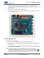
2.2.3 CDB47xxx-DCxx Daughter Card
The layout for the daughter card shipped with the CDB47xxx is the same, regardless of which type of
main board (differential or single-ended) the customer orders. The daughter card can be ordered
populated with either the CS47048, Cs47028, or CS47024 DSP. Figure 2-4 shows the top side of the
CDB47xxx-DC48 daughter card. The accompanying legend identifies the main components of the board.
DS886DB4
Copyright 2009 Cirrus Logic, Inc
2-6
Identifying CDB47xxx Components
CDB47xxx User’s Manual
10
8
11
9
7
6
5
4
3
2
1
Figure 2-4. CDB47xxx-DC48 Daughter Card
2.2.3.1 CDB47xxx-DC48 Daughter Card Components
The circled numbers found in Figure 2-4 refer to the CDB47xxx-DC48 Daughter Card components in the
following list.
1. Cirrus Logic CS47048 DSP
2. Power LEDs (2)
3. MCLK-XTAL_OUT Header
4. DSP GPIO Button
5. DSP GPIO LED
6. DSP GPIO LED
7. DSP GPIO Switch
8. +1.8VD Probe Point
2-7
Copyright 2009 Cirrus Logic, Inc.
DS886DB4
Identifying CDB47xxx Components
CDB47xxx User’s Manual
9. +3.3VD Probe Point
10. +1.8VA Probe Point
11. +3.3VA Probe Point
§§
DS886DB4
Copyright 2009 Cirrus Logic, Inc
2-8
Installation, Setup, and Running First Application
CDB47xxx User’s Manual
Chapter 3
Installation and Setup of Development Board Software
3.1 Installation, Setup, and Running First Application
It is important to install the CDB47xxx Board software before connecting the USB cable
from the PC to the USB port of the CDB47xxx Board. Failure to install the evaluation
software before the initial connection can result in an inability to communicate with the
CDB47xxx.
3.1.1 Evaluation Software Installation
The DSP evaluation software installation will first install the Cirrus Logic® DSP evaluation software
followed by the USB drivers required to communicate with the CDB47xxx board.
1. Run the latest DSP evaluation software installation executable (CS47xxx_eval_kit_build**.exe or
later). This executable is supplied by your Cirrus Logic representative.
2. At the Welcome screen, click Next.
3. At the Cirrus Logic Licensing Agreement window, select the “I accept the agreement” radio button to
agree to the terms and then select Next.
4. Select the default destination directory suggested by the installer for downloading the evaluation kit
files.
5. Select the default directory suggested by the Installer for storing the shortcuts to the programs and
files you are downloading.
6. Clink the Install button to begin the installation process.
7. Click the Finish button to complete the installation process.
3.1.2 Setting up the CDB47xxx Board with a DVD Player
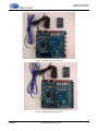
Follow these steps to set up the CDB47xxx Board
1. Place the CDB47xxx and the CDB47XXX-DCxx daughter card on a static-free surface.
2. If the boards are not connected, connect them together as shown in Figure 3-1.
3. Connect the power supply jack to the CDB47xxx Board at J2 and the adapter to a wall power socket
or to a power strip.
Note: Never connect the power supply without the daughter card being connected to the main board.
The switching regulators on the main board rely on voltage sensing paths provided by the
daughter card. Opening these paths will cause the regulator ouput to reach potentially
damaging voltages.
4. Ensure that the D14 (blue), D7 (green), D8 (yellow), and D9 (red) power indicator LEDs on the
CDB47xxx illuminate when power is applied to the board.
3-1
Copyright 2009 Cirrus Logic, Inc.
DS886DB4
Installation, Setup, and Running First Application
CDB47xxx User’s Manual
5. Make Audio Input connections to the CDB47xxx Board.
•
Connect one end of the digital audio S/PDIF optical cable to (J1) on the CDB47xxx Board.
•
Connect the other end of the optical cable to the optical output on the back of a DVD player or other
digital audio source.
6. Make Audio Output connections from the CDB47xxx Board:
•
From the main Analog Line-level Outputs on the CDB47xxx, connect powered speakers to J5 and
J10 using RCA audio cables.
Figure 3-1. CDB47xxx Board with CDB47xxxD (or S)-DC-xx Daughter Card Attached
3.1.3 Connecting to a PC
Follow these steps, to connect the
1. Connect the “B” end of the USB cable to P1 on the USB-Master daughter card.
2. Connect the “A” end of the USB Cable to a USB 2.0 port on a notebook or PC running Windows XP®
operating system.
3. The Windows® operating system should recognize that a new device has been attached and display
a notice saying “Found New Hardware”.
Note: In the Windows® Device Manager, the CDB47xxx appears as a Universal Serial Bus
Controller called “USBXpressDevice”. The Device ID is “CDB47”. The Cirrus Device Manager
(CDM), which is launched after the CDB47xxx Evaluation Kit is installed and thereafter when
the user’s system is rebooted, displays the Device name as “CS47xxx_board”. Look for the
CDM icon at the bottom of the right side of the computer screen.
DS886DB4
Copyright 2009 Cirrus Logic, Inc
3-2
Installation, Setup, and Running First Application
CDB47xxx User’s Manual
Caution: The Cirrus Device Manager must be running in order for the board to operate correctly.
3.1.4 Running a Stereo PCM SPDIF In, DAC Out Application on CDB47xxx
Launch DSP Composer (Start →Program→Cirrus DSP→CS47XXX→DSPComposer).
1. In DSP Composer, go to File→Open and open C:\CirrusDSP\CS47xxx\projects\spdif_in_dacout.cpa.
Note: If the pop up window “Project Out of Date” apprears, click on “Update Devices”.
2. Press the Go button
3. Insert PCM material into the DVD player (e.g., music CD). If a DVD is being used as the audio source,
make sure that the DVD Player (or other digital audio source) is configured to output PCM data.
Note: Press Play on the DVD player (or other digital audio source). You should now hear audio from
the speakers.
3.1.5 Running a Stereo ADC In, DAC Out Application on CDB47xxx
Launch DSP Composer (Start→Program→Cirrus DSP→CS47XXX→DSPComposer)
1. In DSP Composer, go to File→Open and open C:\CirrusDSP\CS47xxx\projects\adc_in_dacout.cpa.
Note: If the pop up window “Project Out of Date” appears, click on “Update Devices”.
2. Press the Go button
3. Provide analog audio input signals to inputs AIN_1A (J14) and AIN_1B (J15) of the CDB47xxx. (Full
scale is approximately 4.3Vrms for a differential signal, and approximately 2.15Vrms for single
ended.)
4. You should now hear audio from the speakers.
§§
3-3
Copyright 2009 Cirrus Logic, Inc.
DS886DB4
Installation, Setup, and Running First Application
CDB47xxx User’s Manual
DS886DB4
Copyright 2009 Cirrus Logic, Inc
3-4
Introduction
CDB47xxx User’s Manual
Chapter 4
Programming the CDB47xxx Board
4.1 Introduction
With the exception of the power selection jumpers, the CDB47xxx is configured exclusively through
software. The DSP Composer™ software is a graphical user interface (GUI) that is used to program the
CS470xx DSP, and to configure the CDB47xxx. This chapter provides basic instructions for using the GUI
to control the CDB47xxx. Detailed information on using the DSP Composer™ can be found in the DSP
Composer™ User's Manual. Your local Cirrus Logic representative can assist you in obtaining both the
DSP Composer software and the User's Manual for the software.
4.2 Running the ADC In / DAC Out Example Application
Follow the instructions in Chapter 3 in order to install the USB drivers on your PC and launch the DSP
Composer software (the GUI used to control the CDB47xxx).
After following the instructions in "Running a Stereo ADC In, DAC Out Application on CDB47xxx"on page
3-3”, the DSP Composer main window will appear as shown in Figure 4-1.
The blocks shown in the main window of DSP Composer can be selected from the folders in the left-hand
window pane, and then connected together by “wires” to indicate the processing path
In this example, the Audio In and Audio Out blocks represent the analog input (ADC) and output (DAC)
ports. These blocks can also be configured to represent various combinations of analog and digital I/O
such as I2S and S/PDIF. This is explained later beginning with Section 4.2.2. The terminals on the Audio
In and the Audio Out blocks represent the I/O ports.
The MPM (Matrix Processing Module), VPM (Virtualizer Processing Module, and PPM (Post-Processing
Module) blocks are intended to implement signal processing. In this example, the MPM and VPM blocks
are pass through blocks containing no internal processing.
4-1
Copyright 2009 Cirrus Logic, Inc.
DS886DB4
Running the ADC In / DAC Out Example Application
CDB47xxx User’s Manual
Figure 4-1. ADC In / DAC Out Example
4.2.1 System Block
All designs must contain the System block. In DSP Composer, when you drag the System block onto the
workspace, the dialog box shown in Figure 4-2 is displayed. This dialog box provides options for selecting
the Target chip associated with the development board, the Firmware version (memory map), Core
Speed, Reference Clock Frequency (Ref. clock freq.), and the Autodetect Fs.
Note: Leave the Autodetect Fs default value as "None" unless the application note for a specific
firmware module used in a Composer project provides a setting that differs from the default
value.
Figure 4-2. CDB47xxx System Properties
DS886DB4
Copyright 2009 Cirrus Logic, Inc
4-2
Running the ADC In / DAC Out Example Application
CDB47xxx User’s Manual
4.2.2 Selecting / Changing Audio Input Sources
Configure the audio inputs to the DSP by dragging and dropping the Audio In block onto the workspace.
The dialog box shown in Figure 4-3 then appears. Choose from one of the supported input combinations
as described in the following sections. ADC is selected by default. The input configuration may be
changed later by right-clicking on the Audio In block and selecting Device Properties.
Figure 4-3. Selecting Audio In Source using Device Properties Dialog
Note: All designs must include the Input Remap block. For details, see Section 4.2.3 “Input
Channel Remap” on page 4-4.
4.2.2.1 Audio In via ADC
To deliver analog audio data to the DSP via the CS470xx ADCs, drag the Audio In block to the workspace
and select an input configuration that includes ADC. The ADC2 input includes a 5:1 input multiplexer that
is controlled by the pull-down list, ADC2 Ch 3+4 Input Sel, shown in Figure 4-4.
Figure 4-4. ADC2 Device Properties.
The ADC2 block's terminal names will change to match the physical input terminals that are now active.
For the configuration shown in Figure 4-4, “Ain_2a” and “Ain_2b” are active. If the selection was “Ain_3A/
3B” instead, the terminals would say “Ain_3a” and “Ain_3b.” On the CDB47xxx board, the microphone
input is connected to terminal 6A.
4-3
Copyright 2009 Cirrus Logic, Inc.
DS886DB4
Running the ADC In / DAC Out Example Application
CDB47xxx User’s Manual
4.2.2.2 Audio In via S/PDIF
To deliver digital audio data to the DSP via the S/PDIF receiver built into the CS47048 and CS47028
devices, drag the Audio In block to the workspace and select an input option that includes S/PDIF as
shown in Figure 4-5.
Figure 4-5. Selecting ADC2 input Terminals using Device Properties Dialog
4.2.2.3 I2S Audio Input
To deliver data to the DSP via I2S, drag the Audio In block to the canvas and choose an input combination
that includes I2S as shown in Figure 4-6. As stated in the dialog box, you must connect an I2S Signal
before pressing “GO!”
Figure 4-6. Selecting Multi-Channel I2S Input
4.2.3 Input Channel Remap
All designs, regardless of the input sources chosen, must include the Input Remap block which maps the
input sources to the internal channels of the DSP. Drag the Input Remap block to the workspace, rightclick on the Remap Audio Input block, and choose Device Properties. Figure 4-7 shows the channel map/
remap options that are available.
DS886DB4
Copyright 2009 Cirrus Logic, Inc
4-4
Running the ADC In / DAC Out Example Application
CDB47xxx User’s Manual
Figure 4-7. Input Remap Device Properties
After selecting the combination of channels to map or remap, the channel wiring options appear in the
Remap Audio Input block. Channels that are not available, now appear as No Connects (NC). By
changing from an option with a smaller number of channels to map, such as “2/0 L/R,” to another option
that maps more channels, such as “3/4 L, C, R, Ls, Rs, Lb, Rb,” all the NO Connects go away and
become available for wiring.
Enter the Wire Mode (Ctrl + w) of DSP Composer to make the following wiring connections:
•
From the outputs of the Audio In block to the inputs of the Input Remap block.
•
From the output of the Input Remap block to the input of the MPM processing block
•
From the output of MPM to the input of VPM
•
From the output of VPM to the input of PPM
•
From the output of PPM to the input of the Output Remap block
•
From the output of the Output Remap block to the input of the Audio Out block
4.2.4 Output Channel Remap
All designs, regardless of the output configuration chosen, must include the Output Remap block which
maps the internal channels of the DSP to the output channels. Drag the Output Remap block to the
workspace.(The Output Remap block has no Device Properties to edit.) Use the Composer Wire mode
(Ctrl + w) and draw wires from the output terminals of the Output Remap block to the desired terminals of
the Audio Output block discussed in the next section, “Selecting the Audio Output Configuration”
4.2.5 Selecting the Audio Output Configuration
Configure the audio outputs to the DSP by dragging and dropping the Audio Out block onto the
workspace. The dialog box shown in Figure 4-8 appears. Choose from one of the supported output
combinations as described in the subsections, Section 4.2.5.1 to Section 4.2.5.3. DAC is selected by
default. The input configuration may be changed later by right clicking on the Audio Out block and
selecting Device Properties.
The Device Properties dialog box allows the user to configure one or more of the following:
4-5
•
DAC
•
I 2S
•
S/PDIF Out
Copyright 2009 Cirrus Logic, Inc.
DS886DB4
Running the ADC In / DAC Out Example Application
CDB47xxx User’s Manual
Note that the Device Properties dialog box allows the user to select analog (DAC) outputs only, digital
outputs only, or a mixture of the two. If digital outputs are enabled, then the two drop down lists at the
bottom of the dialog box allow for DAO2 and DAO3 to be configured to output data in either I2S or S/PDIF
format.
4.2.5.1 Audio Out via DAC
To deliver data from the DSP via the Analog Out DAC outputs, drag the Audio Out block to the workspace.
and check Enable Analog output. See Figure 4-8. Notice that the terminal labels “Aout_1” match those of
the RCA output jacks on the board. Draw wires from the Remap Audio Output block to the DAC block for
the desired mappings.
Figure 4-8. Selecting DAC Outputs Only using Device Properties Dialog
4.2.5.2 Audio Out via S/PDIF Out
To output audio data from the DSP via a S/PDIF output, drag the Audio Out block to the workspace, check
the “Enable DAO {0...3} checkbox, and choose “SPDIF (Optical, J1)” from the DAO3 combo box.See
Figure 4-9. Note that the terminals for DAO3 are replaced by the spdif.L and spdif.R terminals. Draw wires
from the Remap Audio Out put block to the Audio Out block for the desired mappings. DAO2 can also be
configured to be a S/PDIF output.
Figure 4-9. Selecting S/PDIF Outputs and I2S Outputs using Device Properties Dialog
DS886DB4
Copyright 2009 Cirrus Logic, Inc
4-6
Running the ADC In / DAC Out Example Application
CDB47xxx User’s Manual
4.2.5.3 I2S Audio Input Output
To output audio data from the DSP via I2S, drag the Audio In block to the canvas and choose an input
combination that includes I2S as shown in Figure 4-10. Draw wires from the Output Remap block to the
Audio Out block for the desired mappings.
Figure 4-10. Selecting I2S Outputs using Device Properties Dialog
4.2.6 Changing Serial Control Protocol (I2C™ or SPI™) / Flash Type
The CDB47xxx is designed to communicate using either I2C™ or SPI™ protocols. In order to change the
communication mode in the DSP Composer application, go to the menu bar and select File Properties,
which brings up the Project Properties dialog. Click on the Advanced button, as illustrated in Figure 4-11,
in order to set the Master Boot Flash type or put a specified I/O pin into a High-Z state. The Flash Type
pull-down menu is used to select which Flash will be used for a Master Boot. The checkbox, when
checked, puts the corresponding pin into the high-impedance state. See Section 5.1.1 for more details.
4-7
Copyright 2009 Cirrus Logic, Inc.
DS886DB4
Running the ADC In / DAC Out Example Application
CDB47xxx User’s Manual
Figure 4-11. CDB47xxx Communication Modes / Flash Type
§§
DS886DB4
Copyright 2009 Cirrus Logic, Inc
4-8
Programming a Serial Flash Device for Master or Slave Boot Operations
CDB47xxx User’s Manual
Chapter 5
Using DSP Composer or Micro-Condenser Application
to Create and Load a Flash Image
5.1 Programming a Serial Flash Device for Master or Slave Boot
Operations
The CDB47xxx is populated with a 32-Mbit SPI (U17), a 512-kbit I2C (U16), and a 32-Mbit SPI (U14)
Flash devices. The SPI Flash (U17), and I2C Flash (U16), devices can be used to store custom DSP
firmware or run-time firmware configuration files. The SPI Flash U14) device is used to store
microcontroller code and DSP firmware.
The CDB47xxx Board can be used to control the CS470xx DSP in Slave mode via the CDB47xxx onboard microcontroller. Or, a Flash Image can be downloaded to a Flash device on either the CDB47xxx or
a customer board from which the CS470xx DSP can boot itself and operate in Master mode. This chapter
describes the following topics:
•
Using DSP Composer to download an image to either the SPI Flash (U17) or the I2C Flash (U16)
device and initiate Master Boot Operations
•
Using Cirrus Logic’s Micro-Condenser application to download an image containing multiple DSP
Composer projects and snapshots to the SPI Flash (U14) device and to control the DSP in Slave
mode.
5.1.1 Using DSP Composer to Create and Load a Flash Image for Master
Mode Operations
The DSP Composer application allows the user to create a project, compile it into a binary image, deploy
the binary image to the Flash device, and to initiate a Master Boot of the CS470xx DSP.
To create and load a Flash image to the DSP on the CDB47xxx Board or a customer board, follow these
steps:
1. Create a conventional Slave Boot DSP Composer project. Click the Go button and check to see if the
project performs in an acceptable manner when compiled.
2. Open the Project Properties dialog by following the File→Properties menu…path. Select one of the
Master Boot options from the Board boot mode/ comm mode pull-down menu. In the example shown
in Figure 5-1, the user has selected the Master I2C protocol option to load the Flash image to the
DSP.
5-1
Copyright 2009 Cirrus Logic, Inc.
DS886DB4
Programming a Serial Flash Device for Master or Slave Boot Operations
CDB47xxx User’s Manual
Figure 5-1. Project Properties Dialog Showing the Selection of the I2C Protocol for Loading the Flash Image
3. Click the Advanced button and choose one the supported Flash types that will be receiving the Flash
image download. When downloading a Flash image to a customer board, customers should consult
their schematics to determine the Flash type to select. If downloading a Flash image to the CDB47xxx
Board, choose the appropriate I2C or SPI Flash device noted in the Flash Type pull-down menu.
Figure 5-2. Selecting Flash Type via the Advanced Properties Dialog Box
DS886DB4
Copyright 2009 Cirrus Logic, Inc
5-2
Programming a Serial Flash Device for Master or Slave Boot Operations
CDB47xxx User’s Manual
The two JP1 checkboxes allow the user to do one of the following:
•
JP1 Pin 12--Check this box to three-state JP1 Pin 12 signal (mute) which leaves the audio outputs
unmuted on the CDB47xxx. This actions allows the user to install an external mute control such as a
DSP GPO.
•
JP1 Pin 16-- Check this box to three state JP1 Pin 16 signal (flash_hold) which releases the DSP
SPI Flash (U17).
•
Check both boxes
•
Leave both boxes unchecked (Default)-Allows the microcontroller to control both JP1 Pin 12 and
JP1 Pin 16 as necessary.
4. Finally, Click the Go button and DSP Composer will compile the project into a binary image, deploy
the image to the Flash device, and initiate a Master Boot of the CS470xx DSP on the CDB47xxx
Board.
5.1.2 Using Micro-Condenser to Create and Load a Flash Image for Slave
Mode Operations
Cirrus Logic’s Micro-Condenser application allows the user to program the MCU SPI Flash (U14) through
the USB port. Once the Flash device is programmed, the user is able to control the CS470xx DSP in
Slave mode while disconnected from the PC. The user can then load and compile up to 20 DSP
Composer projects with up to 20 snapshots for each project into the microcontroller Flash. The user can
then run any of the loaded projects/snapshots onto the DSP running in Slave mode and control the
operation of the firmware using the CDB47xxx on-board navigation buttons and dials.
5.1.2.1 Micro-Condenser Components
•
flasher_micro.exe
This PC tool builds the Flash image containing the DSP Composer deliverables. This tool uses an
XML file as input.
•
flash_image.xml
This is the input file to flasher_micro.exe. This file specifies the following:
-
The desired output format (for example, .txt, .c)
-
Path and folder name of the DSP Composer deliverable
-
Input/output Fs and display_name of the project
-
The snapshots that are to be built into the Flash image, as well as the display name
(display_name) of the image can be displayed on the CDB47xxx Board LCD
-
The start address of the Flash image
-
Whether little or big endian format is used
-
Optional addition of project or snapshot names to the Flash image
5.1.2.2 Micro-Condenser Restrictions/ Conventions
The Micro-Condenser application has the following restrictions/conventions:
5-3
•
Only analog input is supported.
•
DSP Composer projects and snapshots currently are not identified by the name of the project or
snapshot on the CDB47xxx LCD. They are identified by a number that is derived from the order in
which the project/snapshot appears in the XML file used by Micro-Condenser when it generates the
Flash image. A useful practice is to compile a list of the projects/snapshots created and the number
associated with them in the XML file.
Copyright 2009 Cirrus Logic, Inc.
DS886DB4
Programming a Serial Flash Device for Master or Slave Boot Operations
CDB47xxx User’s Manual
•
Snapshot 0 is the initial configuration that is generated by DSP Composer when the Go button is
pressed and is stored in the file, initial.cfg
5.1.3 Using Micro-Condenser to Create and Load a Flash Image into the
DSP
5.1.3.1 Creating a Flash Image
To use the Micro-Condenser application to create and load a Flash image to the CS470xx DSP on the
CDB47xxx Board, follow these steps:
Follow these steps to create the Flash image:
1. Complete examples are included with the evaluation kits:
C:\CirrusDSP\micro_condenser\CS47XXX\example
2. Use DSP Composer to create the desired Composer Project Archive (.cpa) files. If more than one
setting of the DSP code is desired, you must save the desired settings as snapshots using the
snapshot manager (Tools →Snapshots). This has been done in the .cpa example files.
3. When you have created all the desired snapshots, create the initial setting. Note that the initial setting
is only generated when you press “Go”. This means you must change the configuration in DSP
Composer and then press “Go”, after that save your .cpa file.
4. Generate Deliverables using the drop-down menu option Tools →Generate Deliverables.
5. Repeat steps 1 through 3 for each .cpa file.
6. Specify the projects and snapshots that are to be included in the Flash image, which is accomplished
within an XML file, for the included example refer to:
C:\CirrusDSP\micro_condenser\projects\sample\flash_image.xml
7. Build the Flash image. Open the Console window, navigate to the example folder containing the file,
flash_image.xml
8. Run the file create_flash_image.bat, which contains the statement flasher_micro.exe
flash_image.xml which builds the Flash image.
9. Open flash_image.txt to see the new Flash image data.
5.1.3.2 Programming the Flash Image into the Flash Device
Cirrus provides the usb_flash.exe utility with the CDB47xxx Evaluation Kit and is used to program
memory storage devices. Run program_mcu_spi_flash.bat to program flash_image.txt into the
microcontroller's external SPI Flash. The program_mcu_spi_flash.bat file calls the usb_flash.exe utility to
program the flash_image.txt into the SPI Flash Device.
§§
DS886DB4
Copyright 2009 Cirrus Logic, Inc
5-4
Introduction
CDB47xxx User’s Manual
Chapter 6
CDB47xxx Schematics
6.1 Introduction
The schematics included in this document are the original Revision A schematics of the CDB47xxx and
reflects the board as it was manufactured. Newer schematics may be available that incorporate feature
additions or corrections, and may not match Rev. A hardware.
6.2 CDB47xxS Single-Ended Schematic Descriptions
6.2.1 CDB47xxxS Block Diagram
Figure 6-1 shows the CDB47xxxS block diagram
6.2.2 Daughterboard Connectors
Figure 6-3 shows the schematic for the daughterboard connectors on the CDB47xxxS board.
The digital connector (J2) carries the following signals:
•
Serial Control signals for host control of the CS470xx
•
Serial Control signals from CS470xx to the SPI Flash and I2C EEPROM
•
Serial Audio Data and Clocks going to the DAI of the CS470xx
•
Serial Audio Data and Clocks coming from the DAO of the CS470xx
The analog connector (J3) carries the following signals:
•
8 channels of line-level analog from the CS470xx DACs - can support differential or single-ended
signaling
•
12 channels of line-level analog to the CS470xx ADCs - can support differential or single-ended
signaling
The microphone input is routed to AIN_6A. The AIN_6B channel can be used for mono line-level input.
6.2.3 Digital Audio and Control Connectors
Figure 6-4 shows the schematics for the digital audio and control connectors on the CDB47xxxS board.
The audio input connectors consist of the following:
6-1
•
1 RCA jack for coaxial S/PDIF input
•
1 optical jack for optical S/PDIF input
•
1 2x10 header for serial audio data (I2S)
Copyright 2009 Cirrus Logic, Inc.
DS886DB4
CDB47xxS Single-Ended Schematic Descriptions
CDB47xxx User’s Manual
The audio output connectors consist of the following:
•
1 RCA jack for coaxial S/PDIF output
•
1 optical jack for S/PDIF output
•
1 2x10 header for serial audio data (I2S)
There is one control connector - JP1. This 20-pin connector provides pins for the following functions:
•
Serial control interface for configuring the DSP
•
Reset line for the DSP
•
Proprietary serial debug interface
Jumper (J28) can be used to bypass the on-board MCU and enable use of JP1. While this header is
configured for MCU control (pins 2-3), the MCU will continue to drive all control lines to the CS470xx.
6.2.4 Memory
Figure 6-5 shows the schematic for the SPI Flash and I2C EEPROM devices. The CDB47xxxS is
designed with 32Mbits of SPI Flash and 512 kBit on-board. The serial control port for each device is
routed to the daughtercard connector J2.
6.2.5 Microphone Preamplifier
Figure 6-6 shows the microphone preamplifier for the CDB47xxxS, which has a 1/8” microphone input
jack to allow direct connection to an encapsulated condenser microphone (ECM). Because the output of
the ECM is so small, a pre-amplifier is needed to boost the signal to a line-level voltage.
These specifications for the amplifier are noted on the schematic page. These parameters should be
considered when choosing the microphone to be connected to the CDB47xxxS. Too large of a signal on
the ADC input will result in distortion of the sampled signal.
It is important to note that although the amplifier circuit shown is non-inverting (the input to U19-B is the
same polarity as the output from U19-C), the output of an ECM is inherently inverted since it acts as an
open-collector device. Therefore the microphone signal driven to the CS470xx should be considered an
inverted signal for processing purposes.
6.2.6 Power
Figure 6-7 shows the schematics for power on the CDB47xxxS board.
The DC input connector (J22) for the CDB47xxxS can accept +9 to +12 VDC, and the power supply should
be capable of supplying at least 2 amps of current.
The 4 voltage regulators on the CDB47xxxS generate the +1.8V, +3.3V, +5V and -5V necessary for
powering all of the ICs on the board. Note that the +5V, +3.3V and +1.8V regulators run directly off the DC
input supply connected to the CDB47xxxS. Also notice that the +1.8 V regulator is dependent upon +3.3V
power to enable it (not necessarily the 3.3 V regulator).
The 3 power jumpers (P1-P3) are used to choose between the on-board regulators, and an external
source for +5V, +3.3V, and +1.8V. This is a feature intended only for special applications, so these
jumpers should be left populated for normal operation.
6.2.7 Input Filters
Figure 6-8 shows the input CDB47xxxS. Each input of the CS470xx has its own input filter that consists of
a current limiter, an AC-coupling capacitor (10 μF), and an anti-aliasing capacitor (2200 pF) which is not
DS886DB4
Copyright 2009 Cirrus Logic, Inc
6-2
CDB47xxS Single-Ended Schematic Descriptions
CDB47xxx User’s Manual
populated. The current limiter is scaled to make the CDB47xxxS capable of accepting analog signals of
up to 2 VRMS. The CS470xx analog inputs register full-scale for an input amplitude of 2VRMS with this
input filter.
6.2.8 Output Filters
Figure 6-9 shows the output filters for the CDB47xxxS.
Each output of the CS470xx has an output filter that consists of an AC-coupling cap (22 μF), a pull-down
resistor to prevent the output from floating when not connected to a load, a series resistor (560 Ω) to
provide a voltage drop when the muting transistor is enabled, a filter cap (2200 pF) and a mute transistor
that will pull the output low when the mute control signal is enabled. The series resistor is small enough
that it does not affect the signal in normal operation, assuming a load of at least 5 kΩ is connected to the
analog output of the board.
6.2.9 MCU Block Diagram
Figure 6-10 shows the MCU block diagram for the CDB47xxxS.
6.2.10 MCU
Figure 6-10 shows the MCU for the CDB47xxxS.
The USB connector (J25) is connected directly to the MCU (U15). All PC control must pass through the
MCU, since it has an integrated USB interface.
Due to the way the MCU multiplexes its serial control pins, and the multiplexing of the pin functions on the
CS470xx, there are two I2C bus isolators (U12 and U13) to prevent slave Comm ports from receiving
commands not intended for them.
The MCU has its own 32 Mbit SPI Flash (U14) for storing MCU firmware.
The LCD control port is multiplexed with other functions on the board, so a buffer (U20) is used to isolate
those logic lines from the LCD data when the MCU is refreshing the LCD display.
The button S6 is the board reset. When the MCU is reset, it reboots and re-initializes the entire board
according to the firmware stored in its internal Flash.
J36 is used only for updating the firmware in the MCU, and has no function in relation to the CS470xx.
6.2.11 User Interface Devices
Figure 6-12 shows the buttons, LEDs, and InfraRed receiver which comprise the standalone user
interface for the CDB47xxxS.
The four momentary contact push-button switches (S1-S4) are routed to the ADC in the MCU (U15).
The rotary encoder with integrated push-button switch (S6) is also routed to the ADC in the MCU (U15).
The LCD (LCD1) is the primary feedback device for the MCU user interface.
The LEDs D1-D4 are also part of the MCU feedback interface showing the MCU status.
LED D11 is used to indicate that the USB interface is active.
6-3
Copyright 2009 Cirrus Logic, Inc.
DS886DB4
DS886DB4
SPDIF - IN
COAX
I2S HDRs
SPDIF - IN
OPTICAL
Header will be available to probe / bring in I2S signals
CDB47XXXS
I2S IN HDR
20 Pin HDR
Standard 20 Pin Debug Header (Serial Control & Debug)
Buffer
Mic
Pre-Amp
Circuitry
Digital
DSP Daughtercard
Mic Input
Jack
The Chronos DSP Daughercard will have only the DSP.
This allows us to easily swap out the DSP for different
CS47xxx Family members.
Analog
Digital
DAO Buttons/LEDs
RCA
IN
2 ch (x4)
RCA IN
2ch
DAO pins on Chronos are also GPIO. These buttons/LEDs
Can be used by the new primitives being developed
GPIO
Use
DaughterCard
SRC
SPDIF
Rx
I2S in
(8 ch)
CS47xxx
DSP CORE
I2S out
(8 ch)
DAC
Digital
I2S OUT
HDR
(8 ch)
Analog
Control
Control
EXT CTRL
SEL
ADC
SPDIF Tx
Control
SMALL
20-PIN HDR
5:1
mux
ADC
8ch
RCA
OUT
Digital
SPI_HOLD
SPI
FLASH
I2C
FLASH
USB MCU
Silicon Labs
GPIO
Control (Parallel Port)
Buffer
LCD Panel
USB
(DSP
Composer)
Power In
Wall Adapter
Power
LEDs
SPDIF - OUT
OPTICAL
Buttons
B1
B2
B3
SPDIF - OUT
COAX
B4
6-4
Figure 6-1. CDB47xxxS (Sngle-ended) Board Block Diagram
Rotary Knob
CDB47xxS Single-Ended Schematic Descriptions
CDB47xxx User’s Manual
Copyright 2009 Cirrus Logic, Inc
GPIO
HDR
CDB47xxS Single-Ended Schematic Descriptions
CDB47xxx User’s Manual
Figure 6-2. CDB47xxS (Sngle-ended) Board Schematic Index
6-5
Copyright 2009 Cirrus Logic, Inc.
DS886DB4
DS886DB4
CDB47xxS Single-Ended Schematic Descriptions
CDB47xxx User’s Manual
Copyright 2009 Cirrus Logic, Inc
6-6
Figure 6-3. CDB47xxxS (Sngle-ended) Daughter Card Connectors
DS886DB4
CDB47xxS Single-Ended Schematic Descriptions
CDB47xxx User’s Manual
Copyright 2009 Cirrus Logic, Inc
6-7
Figure 6-4. CDB47xxxS (Sngle-ended) Digital Audio Control Connectors
DS886DB4
6-8
CDB47xxS Single-Ended Schematic Descriptions
CDB47xxx User’s Manual
Copyright 2009 Cirrus Logic, Inc
Figure 6-5. CDB47xxxS (Sngle-ended) Serial Memory
DS886DB4
CDB47xxS Single-Ended Schematic Descriptions
CDB47xxx User’s Manual
Copyright 2009 Cirrus Logic, Inc
6-9
Figure 6-6. CDB47xxxS (Sngle-ended) Mic Pre-Amp
DS886DB4
6-10
CDB47xxS Single-Ended Schematic Descriptions
CDB47xxx User’s Manual
Copyright 2009 Cirrus Logic, Inc
Figure 6-7. CDB47xxxS (Single-ended) Power Connectors
DS886DB4
CDB47xxS Single-Ended Schematic Descriptions
CDB47xxx User’s Manual
Copyright 2009 Cirrus Logic, Inc
6-11
Figure 6-8. CDB47xxxS (Sngle-ended) ADC Filters
DS886DB4
CDB47xxS Single-Ended Schematic Descriptions
CDB47xxx User’s Manual
Copyright 2009 Cirrus Logic, Inc
6-12
Figure 6-9. CDB47xxxS (Sngle-ended) DAC Filters
DS886DB4
CDB47xxS Single-Ended Schematic Descriptions
CDB47xxx User’s Manual
Copyright 2009 Cirrus Logic, Inc
6-13
Figure 6-10. CDB47xxxS (Sngle-ended) Microcontroller Card Interface
DS886DB4
CDB47xxS Single-Ended Schematic Descriptions
CDB47xxx User’s Manual
Copyright 2009 Cirrus Logic, Inc
6-14
Figure 6-11. CDB47xxxS (Sngle-ended) Microcontroller Card User Interface
DS886DB4
CDB47xxS Single-Ended Schematic Descriptions
CDB47xxx User’s Manual
Copyright 2009 Cirrus Logic, Inc
6-15
Figure 6-12. CDB47xxxS (Sngle-ended) Microcontroller Card User Interface
CDB47xxD Differential Schematic Descriptions
CDB47xxx User’s Manual
6.3 CDB47xxD Differential Schematic Descriptions
6.3.1 CDB47xxxD Block Diagram
Figure 6-13 shows the CDB47xxxD block diagram
6.3.2 Daughterboard Connectors
Figure 6-15 shows the schematic for the daughterboard connectors on the CDB47xxxD board.
See section Section 6.2.2 for description of circuitry.
6.3.3 Digital Audio and Control Connectors
Figure 6-16 shows the schematics for the digital audio and control connectors on the CDB47xxxD board.
See section Section 6.2.3 for description of circuitry.
6.3.4 Memory
Figure 6-17 shows the schematic for the Flash memory devices.
See section Section 6.2.4 for description of circuitry.
6.3.5 Microphone Preamplifier
Figure 6-18 shows the microphone preamplifier for the CDB47xxxD.
See section Section 6.2.5 for description of circuitry.
6.3.6 Power
Figure 6-19 shows the schematics for power on the CDB47xxxD board.
See section Section 6.2.6 for description of circuitry.
6.3.7 Input Filters
Figure 6-20 shows the input CDB47xxxD. Each channel of the CS470xx is differential and input has its
own input filter that consists of a current limiter, an AC-coupling capacitor (10 μF), and an anti-aliasing
capacitor (2200 pF) which is not populated. The current limiter is scaled to make the CDB47xxxD capable
of accepting analog signals of up to 4VRMS differentially.
6.3.8 Output Filters
Figure 6-21 shows the output filters for the CDB47xxxD.
Each channel of the CS470xx is differential and is fed to an op-amp that converts the differential signal
into a single-ended output with a maximum swing of 2 VRMS.
Each output has a series resistor (560 Ω) to provide a voltage drop when the muting transistor is enabled,
and a mute transistor that will pull the output low when the mute control signal is enabled. The series
resistor is small enough that it does not affect the signal in normal operation, assuming a load of at least
5 kΩ is connected to the analog output of the board.
DS886DB4
Copyright 2009 Cirrus Logic, Inc
6-16
CDB47xxD Differential Schematic Descriptions
CDB47xxx User’s Manual
6.3.9 MCU Block Diagram
Figure 6-22 shows the MCU block diagram for the CDB47xxxD.
6.3.10 MCU
Figure 6-23 shows the MCU for the CDB47xxxD.
See section Section 6.2.10 for description of circuitry.
6.3.11 User Interface Devices
Figure 6-12 shows the buttons, LEDs, and InfraRed receiver which comprise the standalone user
interface for the CDB47xxxD.
See section Section 6.2.11 for description of circuitry.
6-17
Copyright 2009 Cirrus Logic, Inc.
DS886DB4
DS886DB4
CDB47XXXD
I2S HDRs
SPDIF - IN
COAX
Header will be available to probe / bring in I2S signals
SPDIF - IN
OPTICAL
I2S IN HDR
20 Pin HDR
Standard 20 Pin Debug Header (Serial Control & Debug)
Mic
Pre-Amp
Circuitry
Digital
Buffer
DSP Daughtercard
The Chronos DSP Daughercard will have only the DSP.
Diff
Amp
This allows us to easily swap out the DSP for different
CS47xxx Family members.
DAO Buttons/LEDs
Stereo 1/8"
IN
2 ch (x4)
Analog
Digital
DAO pins on Chronos are also GPIO. These buttons/LEDs
Can be used by the new primitives being developed
GPIO
HDR
Stereo 1/8"
IN
2ch
GPIO
SPDIF
Rx
I2S in
(8 ch)
CS47xxx
SRC
DSP CORE
ADC
I2S out
(8 ch)
Digital
I2S OUT
HDR
(8 ch)
DAC
Analog
Control
Control
SMALL
20-PIN HDR
5:1
mux
ADC
SPDIF Tx
Control
EXT CTRL
SEL
Copyright 2009 Cirrus Logic, Inc
Use
DaughterCard
Diff
Amp
Digital
SPI_HOLD
SPI
FLASH
I2C
FLASH
USB MCU
Silicon Labs
8ch
RCA
OUT
GPIO
Control (Parallel Port)
Buffer
Power In
Wall Adapter
Power
LEDs
B1
B2
B3
SPDIF - OUT
COAX
SPDIF - OUT
OPTICAL
B4
Figure 6-13. CDB47xxD (Differential) Board Block Diagram
Rotary Knob
6-18
CDB47xxD Differential Schematic Descriptions
CDB47xxx User’s Manual
Buttons
LCD Panel
USB
(DSP
Composer)
Mic Input
Jack
CDB47xxD Differential Schematic Descriptions
CDB47xxx User’s Manual
Figure 6-14. CDB47xxD (Differential) Board Schematic Index
6-19
Copyright 2009 Cirrus Logic, Inc.
DS886DB4
DS886DB4
Copyright 2009 Cirrus Logic, Inc
CDB47xxD Differential Schematic Descriptions
CDB47xxx User’s Manual
6-20
Figure 6-15. CDB47xxD (Differential) Daughter Card Connectors
DS886DB4
Copyright 2009 Cirrus Logic, Inc
CDB47xxD Differential Schematic Descriptions
CDB47xxx User’s Manual
6-21
Figure 6-16. CDB47xxD (Differential) Digital Audio Control Connectors
DS886DB4
Copyright 2009 Cirrus Logic, Inc
6-22
CDB47xxD Differential Schematic Descriptions
CDB47xxx User’s Manual
Figure 6-17. CDB47xxD (Differential) Digital Serial Flash
DS886DB4
Copyright 2009 Cirrus Logic, Inc
CDB47xxD Differential Schematic Descriptions
CDB47xxx User’s Manual
6-23
Figure 6-18. CDB47xxD (Differential) Mic Pre-Amp
DS886DB4
Copyright 2009 Cirrus Logic, Inc
CDB47xxD Differential Schematic Descriptions
CDB47xxx User’s Manual
6-24
Figure 6-19. CDB47xxxD (Differential) Power Connectors
DS886DB4
Copyright 2009 Cirrus Logic, Inc
6-25
CDB47xxD Differential Schematic Descriptions
CDB47xxx User’s Manual
Figure 6-20. CDB47xxD (Differential) ADC Filters
DS886DB4
Copyright 2009 Cirrus Logic, Inc
CDB47xxD Differential Schematic Descriptions
CDB47xxx User’s Manual
6-26
Figure 6-21. CDB47xxD (Differential) Voltage Output Circuitry
DS886DB4
Copyright 2009 Cirrus Logic, Inc
6-27
CDB47xxD Differential Schematic Descriptions
CDB47xxx User’s Manual
Figure 6-22. CDB47xxD (Differential) Microcontroller Card Interface
DS886DB4
Copyright 2009 Cirrus Logic, Inc
CDB47xxD Differential Schematic Descriptions
CDB47xxx User’s Manual
6-28
Figure 6-23. CDB47xxD (Differential) Microcontroller Card Schematic
DS886DB4
Copyright 2009 Cirrus Logic, Inc
6-29
CDB47xxD Differential Schematic Descriptions
CDB47xxx User’s Manual
Figure 6-24. CDB47xxD (Differential) Microcontroller Card User Interface
CDB47xxx-DC48 Daughter Card Schematic
CDB47xxx User’s Manual
6.4 CDB47xxx-DC48 Daughter Card Schematic
6.4.1 CDB47xxx-DC48 Block Diagram
Figure 6-25 shows the CDB47xxx-DC48 block diagram
6.4.2 CDB47xxx-DC48 Schematic
The schematic for the CDB47xxx-DC48 daughter card is shown in Figure 6-26. The CDB47xxx-DC48
employs the CS47048 DSP. The DSP is driven by an external crystal circuit. This fixed 24.576 MHz clock
is used to drive the PLL inside the CS470xx for the core DSP clocks, and for all internal audio clocks.
The DSP has a dedicated reset line (DSP_RESET) that must be driven by the host to initialize the
CS470xx’s communication mode and initiate the first boot sequence. This signal is independent of any
other reset on the board and can be used to sequence device power up.
The host communication protocol of the DSP is determined by the state of the HS[3:0] pins at the rising
edge of reset.
The serial host control port (SCP_CLK, SCP_MOSI, SCP_MISO/SDA, SCP_CS, SCP_IRQ, SCP1_BSY)
is used by the host controller to boot and control the DSP. Note that the pull-up resistors on the SCP_IRQ
and SCP_BSY pins are required for both SPI and I2C control, since these are open-drain pins. The pullups on the SCP_CLK and SC1_SDA pins are required only for I2C operation.
The DSP has a debug port (DBDA, DBCK) that allows a developer to debug the DSP during normal
operation. This is a slave port that can be connected to an I2C master, or it can be simply terminated with
pull-up resistors.
The DAI3 digital audio input pin of the CS470xx is driven by a multiplexer on the CDB47xxx main board
that chooses between optical S/PDIF RX, coaxial S/PDIF RX, and DAI3 from the DAI header on the main
board. The remaining DAI pins are driven directly by the DAI header on the main board.
The DAO port of the CS470xx is driven directly to the DAO header on the main CDB47xxx Board.
The DAC outputs are routed directly to the DAC filter circuitry on the CDB47xxx main board.
The ADC inputs are routed directly to the ADC filter circuitry on the CDB47xxx main board.
The Daughtercard ID register (U2) is used to identify which CS470xx chip is populated on the board. This
register is read by the MCU or the PC in order to determine which DSP firmware is appropriate for the
SOC.
DS886DB4
Copyright 2009 Cirrus Logic, Inc
6-30
DS886DB4
CDB47XXX_DC48
Analog
Connector
DC_ID
SHIFT REG
DAC
OUTPUTS
GPIO
I2S In
Copyright 2009 Cirrus Logic, Inc
I2S Out
Analog
Connector
Serial Control
S/PDIF In
S/PDIF Out
ADC
CS47xxx
LED x 2
INPUTS
SWITCH
BUTTON
Digital
Connector
Current
Measure
Point
Current
Measure
Point
+1.8VD +3.3VA
Current
Measure
Point
+1.8VA
POWER
CONNECTOR
Figure 6-25. CDB47xxx-DC48 Daughter Card Block Diagram
6-31
CDB47xxx-DC48 Daughter Card Schematic
CDB47xxx User’s Manual
+3.3VD
Current
Measure
Point
DS886DB4
Copyright 2009 Cirrus Logic, Inc
CDB47xxx-DC48 Daughter Card Schematic
CDB47xxx User’s Manual
6-32
Figure 6-26. CDB47xxx-DC48 Daughter Card Schematic
Obtaining Schematic Updates
CDB47xxx User’s Manual
6.5 Obtaining Schematic Updates
Updates to the schematics for the CDB47xxx Development Board can be can be obtained from your local
Cirrus Logic representative as part of a design package including the associated BOM, and layout
artwork. The schematics are provided in Adobe’s portable document format (PDF) and PADS™ format.
The schematics included in this document are the original Revision A schematics of the CDB47xxS and D
boards and reflect the boards as they were manufactured. Newer schematics may be available that
incorporate feature additions or corrections, and may not match Rev. A hardware.
§§
6-33
Copyright 2009 Cirrus Logic, Inc.
DS886DB4
Obtaining Schematic Updates
CDB47xxx User’s Manual
DS886DB4
Copyright 2009 Cirrus Logic, Inc
6-34
Troubleshooting Guide
CDB47xxx User’s Manual
Chapter 7
Troubleshooting
7.1 Troubleshooting Guide
This section provides solutions to problems that users might experience when using the CDB47xxx.
7.1.1 Power LEDs
Problem: Power LEDs are not illuminated.
•
Possible cause: DC power supply is not connected to CDB47xxx.
Solution: Ensure the DC wall supply is connected to the DC power input jack (J22), and the
supply is plugged into a wall outlet.
•
Possible cause: Power selection headers (P1-P3) are not populated.
Solution: If you are using the DC wall supply provided with the CDB47xxx, all jumpers should
installed.
•
Possible cause: Jumper settings when using an external power supply are set incorrectly.
Solution: If you are using an external power supply for any of the system voltages (5V, 3.3V,
1.8V), ensure that the jumper for that voltage has been removed and power is applied to pin 2
of the appropriate header.
7.1.2 Board not Recognized by PC
Problem: CDB47xxx is not Recognized by PC
•
Possible cause: DC power supply is not connected to CDB47xxx.
Solution: The CDB47xxx is not a USB-powered device. Make sure the DC wall supply is
connected to the DC power input jack (J22), and the supply is plugged into a wall outlet.
•
Possible cause: CDB47xxx USB Drivers not installed before connecting to PC.
Solution: Follow these steps:
1. Pull the DC power plug on the CDB47xxx.
2. Open the Windows® Device Manager on the PC and search for the “USBXpress Device”
under “USB Controllers”.
3. If there is a question mark next to the device, right click on it and open “Properties.” Press
the Update Driver button and let Windows® operating system automatically find the driver.
4. Wait 3 seconds, and plug the DC power supply back into the power input jack.
7-1
Copyright 2009 Cirrus Logic, Inc.
DS886DB4
Revision History
CDB47xxx User’s Manual
7.1.3 Audio is not Heard
Problem: Audio cannot be heard.
Possible cause: Wrong S/PDIF Source is selected.
Solution: Check to make sure that the LED next to the desired S/PDIF source is ON. If not,
use MCU to select the appropriate S/PDIF input.
Revision History
Revision
Date
DB1
March 13, 2009
DB2
July 2, 2009
DB3
July 6 and 15, 2009
Updated Chapters 1, 2, 3, and 4. Additional changes to the remaining chapters will be made
in the next release.
September 4, 2009
Updated Chapter 4, "Programming the CDB47xxx Board" to include latest changes to DSP
Composer. Added reference to the Cirrus Device Manager in the note in Section 3.1.3 and
added a caution statement immediately after the note. Changed references to the board
name from CDB470xx to CDB47xxx to match the silk screen of the name on the board.
DB4
Changes
Initial Release for CDB47xxx-YSB User’s Manual.
Added new contents for Chapter 3 and 4. Added new Chapter 5 that was not in the DB1
release.
§§
DS886DB4
Copyright 2009 Cirrus Logic, Inc
7-2