1
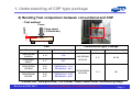
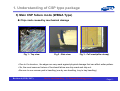
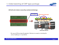
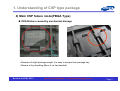
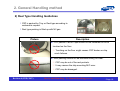
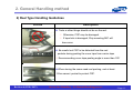
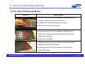
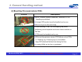
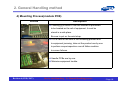
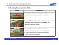
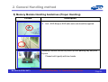
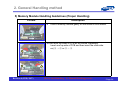
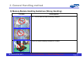
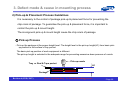
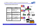
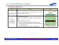
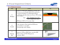
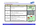
USER’S MANUAL (Chip Scale Package) • To make a win-win situation for CSP products supplier and customer, Samsung provides the information of CSP package’s characteristics and manuals to maintain high quality so that the problems of customer process can be minimized or prevented • Samsung will support the technical information when customer’s request it. Written by Module team .(FEB.2007,Rev.03) Revised by Device Packaging technology team (FEB.2007, Rev.04) Revision 4 (FEB, 2007) One by One Handling, No Manual Handling process - Page 1 - Main contents It says understanding of CSP package, general handling method(box moving, tray, reel, module PCB), defect mode in mounting process(chip crack, cleaning, repair, solder joint reliability) and visual inspection criteria 1. Understanding of CSP 1) Structure comparison between Conventional and CSP 2) Bending Test comparison between conventional and CSP 3) Main CSP failure mode(WBGA Type) 4) Main CSP failure mode(FBGA Type) 5) Operators handling to CSP to be educated thoroughly – Page 3 – Page 4 – Page 5~6 – Page 7 – Page 8 2. General handling method 1) Box conveyance 2) Reel type packing 3) Tray type packing 4) Mounting Process(module PCB) 5) Memory module handling guidelines – Page 9 – Page 10, 11 – Page 12 ~ 14 – Page 15 ~ 22 – Page 23 ~ 28 3. Defect mode in SMT process 1) Chip crack defect 2) Pick-up & Placement Process Guidelines 3) Water cleaning process 4) Repair(reball) method process 5) Solder joint reliability – Page 29 – Page 30 ~ 32 – Page 33 – Page 34 – Page 35 ~ 44 4. Inspection criteria 1) Marking Area 2) Solder Ball Area 3) External area – Page 45 – Page 45~47 – Page 48 ~ 49 Revision 4 (FEB, 2007) One by One Handling, No Manual Handling process - Page 2 - 1. Understanding of CSP type package 1) Structure comparison between Conventional and CSP • CSP type component is very brittle and fragile because of it’s characteristics. That’s why a special attention must be paid to machine jamming and handling before assembled in PCB board and during progress. • CSP(WBGA) has no EMC mold protection, because of it’s size and speed issue so, if it is bumped, dropped or handled carelessly, Mostly function failure occurs. So special caution must be taken.(except : FBGA/TBGA/BOC) Die Substrate (PCB & PI Tape) EMC mold protect Solder ball Gold Wire ENCAP. Die EMC mold protect Gold wire Gold Wire [ BOC ] Die Substrate(PCB) Gold Wire Die Lead frame Die attach adhesive Conventional package Substrate (PCB) EMC mold protect Die Solder ball Gold Wire [ WBGA ] ENCAP. Solder ball Substrate (PCB) [ FBGA ] Chip scale package Revision 4 (FEB, 2007) One by One Handling, No Manual Handling process - Page 3 - 1. Understanding of CSP type package 2) Bending Test comparison between conventional and CSP • Test method Length Force Force speed ( 0.25mm/min) PKG CSP Conventional type Package Device Length (mm) Breakdown point (kgf) 128M SDRAM 54WBGA 0.13 7.16 512M DDR2 60BOC 0.17 5.87 256M GDDR3 144FBGA 0.23 0.48 CHIP Broken : 13.6 PKG Broken: 24.3 256M SDRAM 54FBGA 0.45 0.57 CHIP Broken : 4.30 PKG Broken : 4.85 Device Length (mm) Breakdown point (kgf) 64M SDRAM 54TSOP2 0.17 21.76 256M SDRAM 54TSOP2 0.11 29 • Without EMC Mold protection, CSP is about 4 times weaker than Conventional package. Revision 4 (FEB, 2007) One by One Handling, No Manual Handling process - Page 4 - 1. Understanding of CSP type package 3) Main CSP failure mode (WBGA Type) Chip crack caused by mechanical damage Fig 1 : Top view Fig 2 : Side view Fig 3 : Cell crack(after decap) • Due to it’s structure, the edges are very weak against physical damage that can affect wafer pattern. • So, the most common factors of functional failure are chip crack and chip out. • Be sure to use vacuum pad in handling (one by one handling, tray to tray handling) Revision 4 (FEB, 2007) One by One Handling, No Manual Handling process - Page 5 - 1. Understanding of CSP type package Gold wire broken caused by mechanical damage Encapsulat Mechanical damage Gold wire broken • By very soft Silicone type Encapsulant, Gold wire is covered, so touching this area or handling on it, is prohibited. Revision 4 (FEB, 2007) One by One Handling, No Manual Handling process - Page 6 - 1. Understanding of CSP type package 4) Main CSP failure mode(FBGA Type) PKG Broken caused by mechanical damage • Because of slight package weight, it is easy to escape from package tray. • Becare of tray handling (Move it on tray bended) Revision 4 (FEB, 2007) One by One Handling, No Manual Handling process - Page 7 - 1. Understanding of CSP type package 5) Operators handling to CSP to be educated thoroughly. • CSP(WBGA) is not a conventional package whereby the chip is protected with EMC for physical damage. To handle such a fragile part in the PCB assembly manufacturing environment, exceptional care is required. The operators handling the chip have to be educated thoroughly on the handling procedure. 6) Minimum handling is required. • The layout for CSP package are fully automatic with minimum handling. Revision 4 (FEB, 2007) One by One Handling, No Manual Handling process - Page 8 - 2. General Handling method 1) Box conveyance • Do not open except for approved protective work station • It is recommended surface mount products should be assembled after opening this moisture barrier bag, under 30도/60% R.H within 70 days • deliver the products with specified packing(SEC packing specification) do not change packing material or shape • Do not to strike the box materials with hard objects or step on them • DO not re - packing the box during transfer to user without SEC’s approval • Do not drop the box higher than 70㎝ otherwise inside products will be damaged • Do not fill up more than 6 stack (large size box) Revision 4 (FEB, 2007) One by One Handling, No Manual Handling process - Page 9 - 2. General Handling method 2) Reel Type Handling Guidelines • CSP is packed by Tray or Reel type according to customer’s request. • Reel type packing is filled up with N2 gas. Picture Description z CSP packed Carrier Tape should not be unreeled not to be touched on the floor. ☞ Touching on the floor might causes CSP broken or chip crack failures. z Reel packing should not be distorted during Un-Reel. ☞ CSP may be out of the reel pockets. ☞ It may causes the chip mounting M/C error. ☞ CSP may be damaged. Revision 4 (FEB, 2007) One by One Handling, No Manual Handling process - Page 10 - 2. General Handling method 2) Reel Type Handling Guidelines Picture Description z Tools or other things should not be on the reel. ☞ Otherwise, CSP may be damaged. ☞ If tape hole is damaged, Chip mounting M/C will have error z Be careful not CSP to be distorted from the reel pockets during peeling the cover tape from carrier tape ☞ Recommending cover tape peeling angle is more than 120° z When storing the some-used reel packing, reel at least 50cm vacant pocket to protect CSP. Revision 4 (FEB, 2007) One by One Handling, No Manual Handling process - Page 11 - 2. General Handling method 3) Tray Type Handling Guidelines Picture Description z During CSP handling, use of metallic material (especially tweezers ) is prohibited. z A single CSP must be handled one by one. z Be sure to put on the wrist strap. z Be sure to use vacuum pad in CSP handling. z One by One handling z Keep CSP at a designated location (Tray) and do not deposit a number of CSP in an overlapping way. z Holding or storing CSP in an overlapping way is prohibited. Revision 4 (FEB, 2007) One by One Handling, No Manual Handling process - Page 12 - 2. General Handling method 3) Tray Type Handling Guidelines Picture Description z Be sure to use vacuum pad instead of the hands when inserting or pulling CSP into or from tray. z A single CSP must be handled one by one. z Be sure to put on the wrist strap z Tray containing CSP is susceptible to damage with a slight shock and the secondary damage by dislocation inside tray is possible. z One by One Handling z CSP dislocated inside tray must be moved to its proper position with using vacuum pad. z Loading of tray with CSP dislocated inside tray can cause CSP crack. Revision 4 (FEB, 2007) One by One Handling, No Manual Handling process - Page 13 - 2. General Handling method 3) Tray Type Handling Guidelines Picture Description z when you handle a tray, must check 4 side stacked tray. z when you moves stacked tray, you must benidng it. (minmun 2 side or cross bending) Revision 4 (FEB, 2007) - One by One Handling, No Manual Handling process - Page 14 - 2. General Handling method 4) Mounting Process(module PCB) Picture Description z When jamming occurs in the conveyor belt feeding CSP, those CSP must be stored in tray, handling it one by one with vacuum pad. z Be sure to put on the wrist strap. z If jig loading PCB is kept between equipments during 2nd surface printing process, CSP bumps against equipment , thereby causing WBGA crack. z One by One Handling z If assembled PCBs are handled in an overlapping way, many WBGA cracks might occur. (Never handle assembled products in an overlapping way.) z One by One Handling Revision 4 (FEB, 2007) One by One Handling, No Manual Handling process - Page 15 - 2. General Handling method 4) Mounting Process(module PCB) Picture Description z If assembled PCB falls on the floor, CSP crack occur 100% . z If some PCBs fall on the floor, scope inspection over all fallen PCBs shall be performed. CSP crack defect shall be screened 100% and then subsequent process shall flow. z Be sure to handle it one by one.. z If failure occurs during 2nd surface printing process and 1st surface part with CSP is placed on the equipment bottom, CSP crack will occur. z If product causes failure during printing process, be sure to insert it into Cleaning Jig to clean it. z This is Cleaning Jig insertion status of the modules z failed in the printing process; such products should be z moved also in Jig status after cleaning. z Holding or storing PCB in an overlapping way is prohibited. Revision 4 (FEB, 2007) One by One Handling, No Manual Handling process - Page 16 - 2. General Handling method 4) Mounting Process(module PCB) Picture Description zUse of metallic material (especially Tweezers) in CSP Handling is prohibited. z A single CSP product must be handled one by one. z Be sure to put on the wrist strap z Avoid handling PCBs in an overlapping way when performing visual inspection and never leave modules on the floor. z PCBs must be handled one by one. z When printing process causes PCB failures, store PCBs in Cleaning Jig; if Cleaning Jig is not available, keep CSP attached Surface from facing the floor. z Locating PCBs on the floor is prohibited. Revision 4 (FEB, 2007) One by One Handling, No Manual Handling process - Page 17 - 2. General Handling method 4) Mounting Process(module PCB) Picture Description z Cleaning jig in which PCBs are inserted is prohibited to be located on the rail of equipment; it must be stored in a safe place. Be sure to put on the wrist strap. z If PCB falls on the floor in the unloading process due to equipment jamming, take out the product one by one to perform scope inspection over all fallen modules to screen failures. z Handle PCBs one by one. z Minimize equipment trouble. Revision 4 (FEB, 2007) One by One Handling, No Manual Handling process - Page 18 - 2. General Handling method 4) Mounting Process(module PCB) Picture Description z CSP stored in the scrap box should be taken out one by one for which scope inspection should be performed. Only good products should be flowed to next. z A CSP must be handled one by one. z Be sure to put on the wrist strap. z Placing assembled PCB on Recycle Jig or Recycle Device is prohibited. z One by One Handling z Placing assembled module products on Recycle Jig or Recycle Device is prohibited. z One by One Handling Revision 4 (FEB, 2007) One by One Handling, No Manual Handling process - Page 19 - 2. General Handling method 4) Mounting Process(module PCB) Picture Description z Placing assembled module products on the floor (metallic material, equipment, product) is prohibited. z Jig with PCB attached should be handled as one by one as possible; when Jig is stored in an overlapping way, arrange it in an orderly manner. z Jig with PCB attached must follow Auto Process (loading, unloading, in-process of various equipment) z If manual operation should be performed inevitably, it must be stored in a safe place. Revision 4 (FEB, 2007) One by One Handling, No Manual Handling process - Page 20 - 2. General Handling method 4) Mounting Process(module PCB) Picture Description z When PCBs move (QC X-Ray Inspection, Monitor, etc.) be sure to use the dedicated Jig and it is prohibited to move Jig in an overlapping way. z RIMM products must be handled one by one. z When monitor or QC is performed in unloading stage, it is required to monitor in Jig status, not a single module status. z One by One Handling z When operators take out Jig from Rail to perform monitor or QC in unloading stage, ensure that CSP don’t bump against the equipment. z Holding or storing CSP in an overlapping is prohibited Revision 4 (FEB, 2007) One by One Handling, No Manual Handling process - Page 21 - 2. General Handling method 4) Mounting Process(module PCB) Picture Description z This show the way PCBs are dropped on the equipment due to jamming in the equipment rail; first minimize the equipment trouble and if PCBs fall on the floor, 100% inspection by scope must be performed to screen failures z Minimize equipment trouble when loading PCBs on Recycle Tray in Unloading stage; if loading mistake is occurred, place the products in their proper location and then next process shall flow z Dragging the loaded Recycle Tray on the floor is prohibited. z If the loaded Recycle Tray is dragged on the floor, tray may be tripped on the floor, which causes CSP crack. Revision 4 (FEB, 2007) One by One Handling, No Manual Handling process - Page 22 - 2. General Handling method 5) Memory Module Handling Guidelines (Proper Handling) Picture Description z Anti - ESD Strap or ESD safe work mat should be applied. zMemory module should be picked up from packing tray only one by one. Please hold it gently with two hands Revision 4 (FEB, 2007) One by One Handling, No Manual Handling process - Page 23 - 2. General Handling method 5) Memory Module Handling Guidelines (Proper Handling) Picture Description z Place a memory module gently on the socket in both hands. zPress both top sides of PCB as left thumb, separately. Insert one top side of PCB and then insert the other side. ex) ① → ② or ② → ① 1 1 Revision 4 (FEB, 2007) 2 2 One by One Handling, No Manual Handling process - Page 24 - 2. General Handling method 5) Memory Module Handling Guidelines (Wrong Handling) Picture Description z Do not stack two or more memory modules zDo not grasp two or more memory modules at one time. Revision 4 (FEB, 2007) One by One Handling, No Manual Handling process - Page 25 - 2. General Handling method 5) Memory Module Handling Guidelines (Proper Handling) Picture Description z Do not drop memory modules to the floor. zHandling memory modules near to tool jig is prohibited because Rigid Metals can give memory modules damage. Revision 4 (FEB, 2007) One by One Handling, No Manual Handling process - Page 26 - 2. General Handling method 5) Memory Module Handling Guidelines (Wrong Handling) Picture Description z Do not twist or bow a memory module zDo not stack memory modules in a hand Revision 4 (FEB, 2007) One by One Handling, No Manual Handling process - Page 27 - 2. General Handling method 5) Memory Module Handling Guidelines (Wrong Handling) Picture Description zDo not insert with holding packages and passive elements, it can cause package cracks and detachment of passive elements by higher inserting force zInsert only one memory module at one time, do not insert multiple memory module at the same time. zDo not press both sides of PCB at the same time. zPressing with both hands at the same time may cause solder joint cracks and package cracks by memory module twist and bow, because Inserting force in both sides at the same time is higher about two times than one given separately. Revision 4 (FEB, 2007) One by One Handling, No Manual Handling process - Page 28 - 3. Defect mode & cause in mounting process 1) Chip crack defect • Dislocations of chip on Tray pocket by handling. • Chip-mounter’s improper pick-up position. • Improper Tray loading on Chip - mounter. Recommending Mounting Pick and placer. Picker Collect Steel with bottom side rubber pad(Vacuum sucker) (Steel size should be smaller than Chip size) Placer buffer spring force Max : 250g, Placing conditions (to PCB) The mount height : ±0.1mm (Regarding PCB bow) Pick-up conditions (from Tray and Reel&Tape) The pick-up height : ±0.1mm (Regarding Tray bow) the better the lower ※ Above conditions are for SEC Test and Module process’s conditions, so they might be not suitable for the customer, Please regard them as recommendations. Revision 4 (FEB, 2007) One by One Handling, No Manual Handling process - Page 29 - 3. Defect mode & cause in mounting process 2) Pick-up & Placement Process Guidelines It is necessary to the control of package pick-up & placement force for preventing the chip crack of package. To guarantee the pick up & placement force, it is important to control the pick up & mount height. The incongruent pick up & mount height cause the chip crack of package ① Pick-up Process - Pick-up the package at the proper height level. The height level is the pick-up height(H1) from basic pickup position to the surface of tray pocket. The basic pick-up position of each equipment is different. The pick-up height is selected in the adequate range for preventing excessive down pressure of nozzle Pick-up nozzle Tray or Reel & Tape pocket H1 Package Revision 4 (FEB, 2007) One by One Handling, No Manual Handling process - Page 30 - 3. Defect mode & cause in mounting process ② Placement Process Placement the package at the proper mount level. The mount level is the mount height(H2) from basic pick-up position of package to the surface of PCB. The basic pick-up position of each equipment depends on package size. The mount height is selected in the adequate range for preventing excessive down pressure of nozzle. Pick-up nozzle PCB Revision 4 (FEB, 2007) Package H2 One by One Handling, No Manual Handling process - Page 31 - 3. Defect mode & cause in mounting process ③ Recommend Nozzle & Head unit system -. Recommended the pick-up surface of nozzle is flatness for preventing damage and scratch of package. The nozzle size should be smaller than package size. The inside diameter of nozzle is selected proper size for maintain vacuum pressure for keeping package during nozzle move -. Recommended the head unit system needs an automatic stop function or controller for preventing over pressure to the nozzle or inappropriate mount & pick-up height operation. The head unit must have buffer spring system for decreasing pressure and impact of placement during nozzle down. -. Recommended the placement buffer spring force is maximum 250g. Revision 4 (FEB, 2007) One by One Handling, No Manual Handling process - Page 32 - 3. Defect mode & cause in mounting process 3) Water cleaning process • Basically water cleaning process is not recommended. : Use of No cleaning solder paste is strongly recommended. • If the water cleaning process is inevitably requested, CSP should not contact chain and belt area of the cleaning equipment Fixed manual jig should be used. • Although jig is used for the process, Dip or Ultrasonic cleaning should be avoided. • Sufficient bake after cleaning process is requested to perform completed elimination of moisture and solvent. • Solvent + Ultrasonic cleaning process is not recommended either. ☞ Main point : HCFC141B solvent chemical(or similar chemical)is deadly affected on gold wire broken of the component. Revision 4 (FEB, 2007) One by One Handling, No Manual Handling process - Page 33 - 3. Defect mode & cause in mounting process 4) Repair(reball) method process IC Detach Weak Point Chip crack Side chip thermal stress Gold wire damaged Tape scratch (Cu patter damage) Revision 4 (FEB, 2007) Method - Vacuum tool height optimize - Chip support jig : NO CONTACT JIG - max peak temp:220℃ - No touch on encap - Do cleaning by manual (prohibit : ultrasonic cleaning) - Don’t push the over force on solder ion Vacuum Tool Hot N2 Gas Dressing cleaning Solder Ion Solder burr Copper wicker Detached IC Dressing Cleaning Dry Ball mounting Chip Vacuum Tool CSP Tray One by One Handling, No Manual Handling process Flux bath - Page 34 - 3. Defect mode & cause in mounting process 5) Solder joint reliability(1) Phenomenon • Fig 1,2 : Solder joint crack of the component side after surface mounting : solder joint crack are happened in the side ball of the component • Fig 3 : Magnification the solder joint crack line (fig2) after etching with chemical • Fig 4 : EDX spectrum of IMC( table 1 : IMC composition &, thickness data) Table 1 Fig1 Fig2 Sn Cu Ni Fig3 Revision 4 (FEB, 2007) Metal Atomic % Ni 21 Cu 41 Sn 38 Total 100 IMC THICK 8㎛ Fig4 One by One Handling, No Manual Handling process - Page 35 - 3. Defect mode & cause in mounting process Defect cause • OSP’s (organic solder-ability preservative)pad design does not have any Cu diffusion barrier so, during the re-flow cu in PCB land diffuses to component’s solder ball land and make Cu rich IMC(Ni/Cu/Sn). This Cu rich IMC maker solder joint crack, therefore crack easily occures by mechanical stress Component Cu Ni rich IMC(Ni3Sn) Ni NixCuySnz IMC Cu PCB Cu rich IMC( NixCuySnz) ¾ Cu Diffusion theory : Cu diffuses very fast when it is ¾ It is certain that the Cu rich IMC cannot melted with solder(Sn/Pb) on the high temperature. adhere to the Ni rich IMC, To prevent its outside diffusible speed is more about 10 ~100 times abnormal growth and spalling of the Cu rich than inside speed. IMC, Cu content in solder and reflow condition should be closely controlled Revision 4 (FEB, 2007) One by One Handling, No Manual Handling process - Page 36 - 3. Defect mode & cause in mounting process Fracture mode of pull test comparison between osp and Ni-Au/Cu plating PCB component PCB OSP type Ni-Au/Cu plating type 1% 1% 98% 1% 1% 75% 0% 23% Recommending • PCB Solder ball land type : Non Solder Mask Defined(NSMD), Ni-Au/Cu Plating, • Plating thickness ; Ni : over 3.0㎛, Au : over 0.25 ㎛ • Plating method : electronic plating • PCB land diameter with 1:1 ratio to the component land • Caution (If the using OSP type PCB) -. Rework or repair (thermal stress) - . Mechanical stress (drop, push, etc) Revision 4 (FEB, 2007) One by One Handling, No Manual Handling process - Page 37 - 3. Defect mode & cause in mounting process ※ Remark • Why happened solder joint crack in the side ball of the component ? • Cause : Side ball of the package are take a more stressed than center ball. it is verified by the simulation Component PCB Model :WBGA(double mounting) Component Solder : Sn37Pb PCB Damage point with mechanical stress Revision 4 (FEB, 2007) One by One Handling, No Manual Handling process - Page 38 - 3. Defect mode & cause in mounting process 5) Solder joint reliability(2) Phenomenon Component side PCB side Defect cause Solder ball component PCB No & Insufficient solder paste on PCB solder ball land Package warpage Revision 4 (FEB, 2007) Solder paste PCB bow during SMT re-flow Solder ball cutted One by One Handling, No Manual Handling process - Page 39 - 3. Defect mode & cause in mounting process Recommending • Set up the auto inspection system for check paste volume before component loading step on the PCB • Optimize the the re-flow temperature for surface mounting (PCB bow) • IQC (Component warpage : within 4mil, ball cutting : within 30% of height) • Check the contamination of the solder ball and solder ball land Revision 4 (FEB, 2007) One by One Handling, No Manual Handling process - Page 40 - 3. Defect mode & cause in mounting process 5) Solder joint reliability(3) Phenomenon component PCB Fig 1 Fig 3 Fig 2 Fig 4 Fig 3 : fracture surface of ball on the PCB side The fracture surface become shine by the re-flow heat Fig 4 : fracture surface of ball on the component side The fracture surface become shine by the re-flow heat Revision 4 (FEB, 2007) One by One Handling, No Manual Handling process - Page 41 - 3. Defect mode & cause in mounting process Defect cause • Void in side solder ball that occurred by out gassing from flux of the solder paste in the surface mounting process • Void Generation Mechanism Step 1 CSP Step 1 : There is no solder joint void in component and fracture surface is rough, which is normal. PCB Step 2 Step 2 : During the re-flow, voids can be generated in the ball of the component by the volatilization of the some flux of the paste. Revision 4 (FEB, 2007) One by One Handling, No Manual Handling process - Page 42 - 3. Defect mode & cause in mounting process Step 3 Step 3 : As the re-flow temperature increase, the size of voids are getting bigger by combine small voids. And voids move to the side of the component Step 4 Step 4 : The size of void is maximized at the peak temp of the re-flow. And solder ball can be taken off by the pushing force of gas. The fracture surface become shine by the re-flow heat. Revision 4 (FEB, 2007) One by One Handling, No Manual Handling process - Page 43 - 3. Defect mode & cause in mounting process Recommending • Re - Flow Profile - Dwell time at pre-heating : 150 ~ 175℃ : 60 ~ 100sec - Peak Temp : The better low temperature , MAX 220℃ - dwell time at over 200℃ : 30 ~ 50sec - Profile Condition : should be closely controlled • Solder paste - Paste volume : The better the lower ※ Re-flow condition should be optimized by the design of experience because of difference the component type, PCB type and atmosphere of re-flow process ※ The re-flow profile sharp that the recommended by SEC is tent type. Revision 4 (FEB, 2007) One by One Handling, No Manual Handling process - Page 44 - 4. Visual Inspection Criteria 1.Marking Area Item Criteria Fig. Marking Typography Cutting Reject if marking Typography has been cutting 2. Solder Ball Area Item Criteria Fig. > FBGA(BOC): Reject if Solder ball coplanarity exceeds below criteria 2-1 Ball Coplanarity Ball Size Coplanarity ~0.29 mm 3.2mil (80um) 0.3~0.44mm 4Mil ( 100um) 0.45mm ~ 4.5mil (106.7um) >TBGA : Max 3mil (75um) >FC-BGA / HBGA : Max 6mil(150um) >(U)LGA : Max 4.0mil(100um) > WBGA : Max. 4Mil (100um) Revision 4 (FEB, 2007) One by One Handling, No Manual Handling process - Page 45 - 4. Visual Inspection Criteria 2.Solder Ball Area Item Criteria Fig. • Reject if Solder ball Misplacement exceeds below criteria -. FBGA (BOC) 2-2. Solder Ball Misplacement -. MCP, TBGA, WBGA : Max. 3 mil(75um) -. (U)LGA : Max 80um -. FC-BGA : Max 8mil(200um) 2-3. Double Ball • Reject if Solder Ball is fused or connected with adjacent Balls. It is a defect. 2-4. Missing Ball • REJECT if solder Ball is Missing or incompletely fused in such a way as to cause the PCB Ball Pad pattern to be even slightly exposed. It is a defect. Revision 4 (FEB, 2007) One by One Handling, No Manual Handling process - Page 46 - 4. Visual Inspection Criteria 2.Solder Ball Area Item Criteria 2-5. Damaged Ball • Reject if solder ball cut or crushed over 30% cause the mechnical damage. 2-6. Foreign substance in the ball area Revision 4 (FEB, 2007) Fig. • Conduction Material: Reject for foreign greater then ½ between ball and ball. • Non conduction material: -. Reject if The others Foreign Materials short between ball to ball,and size of foreign material exceeds ball pitch. -. Reject if Spots size exceeds ½ of PCB Size. One by One Handling, No Manual Handling process - Page 47 - 4. Visual Inspection Criteria 3. External area Item 3-1. Warpage Criteria Fig. • Reject if Solder Ball coplanarity exceeds 4Mil • However, even though solder Ball coplanarity is good, if Package is so Bent that Package coplanarity deviates from war-Factor (Wf) criteria. Is is a defect. Wf = PKG Warpage(Unit: Mil) PKG Length(Unit: Inch) Î Reject if Wf is 2.5 or more then. 3-2. Scratch • Any exposure of base matal on PSR areas by scratches is rejectable. (Except edge Area (20mil)) 3-3. Package Burr • Reject if PCB or EMC Burr exceeds 4Mil. • Reject if burr of PCB Plating Line exceeds 10Mil. Revision 4 (FEB, 2007) One by One Handling, No Manual Handling process - Page 48 - 4. Visual Inspection Criteria 3. External area Item 3-4. PSR Coverage 3-5. Flux Contamination 3-6 PCB Broken& Crack (FBGA) Criteria Fig. • Reject if base metal or core is exceeds 6Mil. (Max 150um) • Reject for contamination short between ball and ball ( if there is flux contamination which is romoved by air blow, it is not defect.) • Reject for flux contamination greater then 2.5 x 2.5mm. • If crack Caused by PKG Broken attacks solder ball Land or VIA Hole, it is defect. • If PCB Edge area exceeds 20mils(Length)x20mil (Width), it is defect. • defect if base metal is exposed. (Visual Inspection or scope (X30) Inspection.) THE END Revision 4 (FEB, 2007) One by One Handling, No Manual Handling process - Page 49 -