1
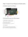
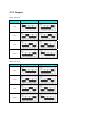
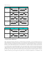
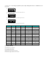
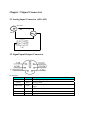
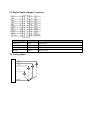
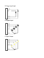
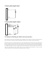
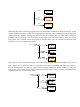
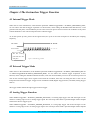
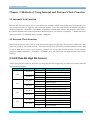
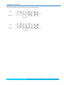
PCI8002A
User’s Manual
Beijing ART Technology Development Co., Ltd.
Contents
Contents.............................................................................................................................................................................. 2
Chapter 1 Overview ........................................................................................................................................................... 3
Chapter 2 Components Layout Diagram and a Brief Description..................................................................................... 5
2.1 The Main Component Layout Diagram................................................................................................................ 5
2.2 The Function Description for the Main Component............................................................................................. 5
2.2.1 Signal Input and Output Connectors ......................................................................................................... 5
2.2.2 Potentiometer ............................................................................................................................................ 5
2.2.3 Jumper ....................................................................................................................................................... 6
2.2.4 Physical ID of DIP Switch......................................................................................................................... 7
2.2.5 Status Indicator.......................................................................................................................................... 8
Chapter 3 Signal Connectors ............................................................................................................................................. 9
3.1 Analog Input Connector (AI0~AI3) ..................................................................................................................... 9
3.2 Signal Input/Output Connector ............................................................................................................................ 9
3.3 Digital Input/Output Connector.......................................................................................................................... 10
3.4 Analog Input....................................................................................................................................................... 10
3.5 Trigger signal input ............................................................................................................................................ 11
3.6 Digital Input ....................................................................................................................................................... 11
3.7 Digital Output..................................................................................................................................................... 11
3.8 Sync pulse signal input....................................................................................................................................... 12
3.9 Sync pulse signal output..................................................................................................................................... 12
3.10 Methods of Realizing the Multi-card Synchronization .................................................................................... 12
Chapter 4 The Instruction Trigger Function .................................................................................................................... 14
4.1 Internal Trigger Mode ........................................................................................................................................ 14
4.2 External Trigger Mode ....................................................................................................................................... 14
4.3 Analog Trigger Function .................................................................................................................................... 14
Chapter 5 Methods of Using Internal and External Clock Function ............................................................................... 16
5.1 Internal Clock Function...................................................................................................................................... 16
5.2 External Clock Function..................................................................................................................................... 16
5.3 A/D Data Bit High Bit Control........................................................................................................................... 16
Chapter 6 Note and Warranty Policy ............................................................................................................................... 18
6.1 Notes .................................................................................................................................................................. 18
6.2 Warranty Policy .................................................................................................................................................. 18
Products Rapid Installation and Self-check...................................................................................................................... 19
Rapid Installation ..................................................................................................................................................... 19
Self-check................................................................................................................................................................. 19
Delete Wrong Installation......................................................................................................................................... 19
Chapter 1 Overview
In the fields of Real-time Signal Processing, Digital Image Processing and others, high-speed and high-precision data
acquisition modules are demanded. ART PCI8002A data acquisition module, which brings in advantages of similar
products that produced in china and other countries, is convenient for use, high cost and stable performance.
ART PCI8002A is a data acquisition module based on PCI bus. It can be directly inserted into IBM-PC/AT or a
computer which is compatible with PCI8002A to constitute the laboratory, product quality testing center and systems
for different areas of data acquisition, waveform analysis and processing. It may also constitute the monitoring system
for industrial production process.
Unpacking Checklist
Check the shipping carton for any damage. If the shipping carton and contents are damaged, notify the local dealer or
sales for a replacement. Retain the shipping carton and packing material for inspection by the dealer.
Check for the following items in the package. If there are any missing items, contact your local dealer or sales.
¾ PCI8002A Data Acquisition Board
¾ ART Disk
a) user’s manual (pdf)
b) drive
c) catalog
¾ Warranty Card
FEATURES
Analog Input
¾
¾
¾
¾
¾
¾
¾
¾
¾
¾
¾
¾
¾
¾
¾
¾
¾
Input Range: ±5V, ±2.5, ±1V, ±0.5V
16-bit resolution
Sampling Rate(sync sample): Max 40MHz; Min 400KHz
Input Channels: 4
Analog Input Mode: Single-ended
Analog Input Impedance: >10MΩ
Chips Number: 4
Data Read Mode: software read mode, DMA mode
Memory: 512K word RAM per channel
Clock Source: Internal clock and external clock
Trigger Mode: software trigger, hardware trigger(external trigger)
Trigger Type: edge trigger
Trigger Direction: negative, positive, either positive or negative trigger
Trigger Level: ±10V
Trigger Sensitivity: 1~65535(819)
Analog Trigger Source: AI0, AI1, AI2, AI3, ATR
System Measurement Accuracy: 0.1%
¾
¾
Operating Temperature Range: 0℃~55℃
Storage Temperature Range: -20℃~70℃
Digital Input
¾
Input channels: 8
¾
¾
¾
¾
Electronic standard: TTL-CMOS
Maximum absorption current: <0.5mA
High level: ≥2V
Low level: ≤0.8V
Digital Output
¾
Output channels: 8
¾
¾
¾
¾
¾
Electronic standard: TTL-CMOS
Pull-down current: ≤20mA
Pull-up current: ≤2.6mA
High level: ≥3.4V
Low level: ≤0.5V
Other features
Board Clock Oscillation: 80MHz
Dimension
170.5mm(L) * 111mm(W)*20mm(H)
Chapter 2 Components Layout Diagram and a Brief Description
2.1 The Main Component Layout Diagram
2.2 The Function Description for the Main Component
2.2.1 Signal Input and Output Connectors
AI0, AI1, AI2, and AI3: Analog signal input ports
J1: Analog signal input and output port
IN: Sync pulse signal input ports
OUT1, OUT2, and OUT3: Sync pulse signal output port
2.2.2 Potentiometer
VR_DAF1: Analog output full-scale adjustment potentiometer
VR_DAZ1: Analog output zero-point adjustment potentiometer
VR_1.25: -2.5V reference power supply adjustment potentiometer
2.2.3 Jumper
Select AI0 range:
Input Range
JP13
JP12
JP15
JP14
±5V
±2.5V
±1V
±0.5V
Select AI1 range
Input Range
±5V
±2.5V
±1V
±0.5V
Select AI2 range
Input Range
JP17
JP16
JP19
JP18
±5V
±2.5V
±1V
±0.5V
Select AI3 range
Input Range
±5V
±2.5V
2.2.4 Physical ID of DIP Switch
DID1: Set physical ID number. When the PC is installed more than one PCI8002A , you can use the DIP switch to set a
physical ID number for each board, which makes it very convenient for users to distinguish and visit each board in the
progress of the hardware configuration and software programming. The following four-bit numbers are expressed by
the binary system: When DIP switch points to "ON", that means "1", and when it points to the other side, that means
"0." As they are shown in the following diagrams: "ID3" is the high bit."ID0" is the low bit, and the black part in the
diagram represents the location of the switch. (Test softwares of the company often use the logic ID management
equipments and at this moment the physical ID DIP switch is invalid. If you want to use more than one device that are
the same type in the same system at the same time, please use the physical ID as much as possible. As for the
differences between logic ID and physical ID, please refer to the function explanations of "CreateDevice" and
"CreateDeviceEx" of The Prototype Explanation of Device Object Management Function in PCI8002AS software
specification).
ON
ID3 ID2 ID1 ID0
ON
DID1
1
2
3
4
The above chart shows"1111", so it means that the physical ID is 15.
ON
ID3 ID2 ID1 ID0
ON
DID1
1
2
3
4
The above chart shows"0111", so it means that the physical ID is 7.
ON
ID3 ID2 ID1 ID0
ON
DID1
1
2
3
4
The above chart shows"0101", so it means that the physical ID is 5.
ID3
OFF(0)
ID2
OFF(0)
ID1
OFF(0)
OFF(0)
0
0
OFF(0)
OFF(0)
OFF(0)
ON(1)
1
1
OFF(0)
OFF(0)
ON(1)
OFF(0)
2
2
OFF(0)
OFF(0)
ON(1)
3
3
OFF(0)
OFF(0)
4
4
OFF(0)
ON(1)
ON(1)
ON(1)
OFF(0)
5
ON(1)
ON(1)
OFF(0)
5
OFF(0)
OFF(0)
ON(1)
6
6
OFF(0)
ON(1)
ON(1)
7
7
ON(1)
OFF(0)
OFF(0)
ON(1)
OFF(0)
8
8
ON(1)
OFF(0)
OFF(0)
9
9
ON(1)
OFF(0)
ON(1)
A
10
ON(1)
OFF(0)
ON(1)
B
11
ON(1)
ON(1)
OFF(0)
C
12
ON(1)
ON(1)
OFF(0)
D
13
ON(1)
ON(1)
ON(1)
ON(1)
OFF(0)
E
14
ON(1)
ON(1)
ON(1)
ON(1)
F
15
2.2.5 Status Indicator
L-ER: Hardware error indicator.
L-TR: Trigger signal indicator.
L-SW: RAM switch indicator.
AD_Busy Led: A/D conversion indicator.
L-PW: Power supply indicator, on for normal.
ID0
ON(1)
OFF(0)
ON(1)
OFF(0)
Physical ID(Hex) Physical ID(Dec)
Chapter 3 Signal Connectors
3.1 Analog Input Connector (AI0~AI3)
BNC Port
Red
+
Black
-
J1
3.2 Signal Input/Output Connector
Pin definition
Name
Color
Description
ATR
Red
AGND
White
Analog ground.
CLKIN/DTR
Green
External clock input.(do not provide for the moment); digital
trigger
CAL
Yellow
1KHz calibrating signal output
SYNOUT
Blue
Internal clock output.
DGND
Black
Digital ground.
Analog trigger signal input.
3.3 Digital Input/Output Connector
Pin Name
Direction
Description
DI0~DI7
Input
Digital input.
DO0~DO7
Output
Digital output
+5V
PWR
+5V power supply
DGND
GND
Digital ground.
3.4 Analog Input
AI0
AI1
AI2
AI3
AGND
3.5 Trigger signal input
ATR
DTR
DGND
AGND
3.6 Digital Input
DI0
DI1
DI2
DI7
DGND
3.7 Digital Output
DO0
DO1
DO2
DO7
DGND
3.8 Sync pulse signal input
IN
DGND
3.9 Sync pulse signal output
OUT1
OUT2
OUT3
DGND
3.10 Methods of Realizing the Multi-card Synchronization
Three methods can realize the synchronization for the PCI8002A, the first method is using the cascade master-slave
card, the second one is using the common external trigger, and the last one is using the common external clock.
When using master-slave cascade card programs, the master card generally uses the internal clock source model, while
the slave card uses the external clock source mode. After the master card and the slave card are initialized according to
the corresponding clock source mode. At first, start all the slave cards, as the main card has not been activated and there
is no output clock signal, so the slave card enters the wait state until the main card was activated. At this moment, the
multi-card synchronization has been realized. When you need to sample more than channels of a card, you could
consider using the multi-card cascaded model to expand the number of channels.
OUT
IN
IN
Master Card
Slave Card 1
Slave Card 2
When using the common external trigger, please make sure all parameters of different PCI8002A are the same. At first,
configure hardware parameters, and use analog or digital signal triggering (ATR or DTR), then connect the signal that
will be sampled by PCI8002A, input triggering signal from ART pin or DTR pin, then click “Start” button, at this time,
PCI8002A does not sample any signal but waits for external trigger signal. When each module is waiting for external
trigger signal, use the common external trigger signal to startup modules, at last, we can realize synchronization data
acquisition in this way. See the following figure:
When using the common external clock trigger, please make sure all parameters of different PCI8002A are the same. At
first, configure hardware parameters, and use external clock, then connect the sampled signal, click “Start” button, at
this time, PCI8002A does not sample any signal, but wait for external clock signal. When all modules are waiting for
external clock signal, use the common external clock signal to startup modules, at last, we realize synchronization data
acquisition in this way. See the following figure:
PCI8002A Data Acquisition
Chapter 4 The Instruction Trigger Function
4.1 Internal Trigger Mode
When A/D is in the initialization, if the hardware parameter ADPara.TriggerMode = PCI8002A_TRIGMODE_SOFT,
we can achieve the internal trigger acquisition. In this function, when calling the StartDeviceProAD function, it will
generate A/D start pulse, A/D immediately access to the conversion process and not wait for the conditions of any other
external hardware. It also can be interpreted as the software trigger.
As for the specific process, please see the figure below, the cycle of the A/D work pulse is decided by the sampling
frequency.
Start Enable
Convert Pulse
The first working
pulse after the A/D
start pulse
Figure 5.1 Internal Trigger Mode
4.2 External Trigger Mode
When A/D is in the initialization, if the hardware parameter ADPara.TriggerMode = PCI8002A_TRIGMODE_DELAY
or ADPara.TriggerMode-PCI8002A_TRIGMODE_MIDL, we can achieve the external trigger acquisition. In this
function, when calling the StartDeviceProAD function, A/D will not immediately access to the conversion process but
wait for the external trigger source signals accord with the condition, then start converting the data. It also can be
interpreted as the hardware trigger. Trigger source includes the DTR (Digital Trigger Source) and ATR (Analog Trigger
Source)
The trigger modes include the edge trigger and level trigger.
4.3 Analog Trigger Function
When ADPara.TriggerDir = PCI8002A_TRIGDIR_NEGATIVE, it is falling edge trigger. The A/D will begin to work
whenever a falling edge occurs on analog trigger signal. The A/D stops when finish a specified length of data sampled
and wait for the next trigger signal.
When ADPara.TriggerDir = PCI8002A_TRIGDIR_POSITIVE, it is rising edge trigger. The A/D will begin to work
whenever a rising edge occurs on analog trigger signal. The A/D stops when finish a specified length of data sampled
BUY ONLINE at art-control.com/englishs or CALL 64862359/64861583(CN)
14
PCI8002A Data Acquisition
and wait for the next trigger signal.
When ADPara.TriggerDir = PCI8002A_TRIGDIR_NEGAT_POSIT, it is either rising or falling edge trigger mode. The
A/D will begin to work whenever a rising edge or falling edge occurs on analog trigger signal. The A/D stops when
finish a specified length of data sampled and wait for the next trigger signal.
BUY ONLINE at art-control.com/englishs or CALL 64862359/64861583(CN)
15
PCI8002A Data Acquisition
Chapter 5 Methods of Using Internal and External Clock Function
5.1 Internal Clock Function
Internal Clock Function refers to the use of on-board clock oscillator and the clock signals which are produced by the
user-specified frequency to trigger the A/D conversion regularly. To use the clock function, the hardware parameters
ADPara.ClockSource = PCI8002A _CLOCKSRC_IN should be installed in the software. The frequency of the clock in
the software depends on the hardware parameters ADPara.Frequency. For example, if Frequency = 100000, that means
A/D work frequency is 100000Hz (that is, 100 KHz, 10uS/point).
5.2 External Clock Function
External Clock Function refers to the use of the outside clock signals to trigger the A/D conversion regularly. The clock
signals are provide by the INCLK pin of J1.
The external clock can be provided by another PCI8002A’s clock output
as well as other device such as clock frequency generators. To use the external clock function, set the hardware
parameters ADPara.ClockSource = PCI8002A_CLOCKSRC_OUT. The A/D sample rate depends on the external clock
frequency.
5.3 A/D Data Bit High Bit Control
Analog input’s data bit is D0~D11, D12 bit is over range flag, D15 bit is trigger flag, D13 and D14 are used to show the
digital input/output status.
Analog Input
Data Bit
AI0_D13
AI0
AI0_D14
AI1_D13
AI1
AI1_D14
AI2_D13
AI2
AI2_D14
AI3_D13
AI3
AI3_D14
Data bit status
Function
0
DI0 edge latch(rising edge valid)
1
DI0 level follow
0
DI1edge latch(rising edge valid)
1
DI1 level follow
0
DI2 edge latch(rising edge valid)
1
DI2 level follow
0
DI3 edge latch(rising edge valid)
1
DI3 level follow
0
DI4 edge latch(rising edge valid)
1
DI4 level follow
0
DI5 edge latch(rising edge valid)
1
DI5 level follow
0
DI6 edge latch (rising edge valid)
1
DI6 level follow
0
DI7 edge latch (rising edge valid)
1
DI7 level follow
BUY ONLINE at art-control.com/englishs or CALL 64862359/64861583(CN)
16
PCI8002A Data Acquisition
Take AI0 for example to show the edge latch and level follow functions:
DI0
AI0_D13
Edge latch
DI0
AI0_D13
Level follow
BUY ONLINE at art-control.com/englishs or CALL 64862359/64861583(CN)
17
PCI8002A Data Acquisition
Chapter 6 Note and Warranty Policy
6.1 Notes
In our products’ packing, user can find a user manual, a PCI8002A module and a quality guarantee card. Users must
keep quality guarantee card carefully, if the products have some problems and need repairing, please send products
together with quality guarantee card to ART, we will provide good after-sale service and solve the problem as quickly
as we can.
When using PCI8002A, in order to prevent the IC (chip) from electrostatic harm, please do not touch IC (chip) in the
front panel of PCI8002A module.
6.2 Warranty Policy
Thank you for choosing ART. To understand your rights and enjoy all the after-sales services we offer, please read the
following carefully.
1. Before using ART’s products please read the user manual and follow the instructions exactly. When sending in
damaged products for repair, please attach an RMA application form which can be downloaded from:
www.art-control.com.
2. All ART products come with a limited two-year warranty:
¾ The warranty period starts on the day the product is shipped from ART’s factory
¾ For products containing storage devices (hard drives, flash cards, etc.), please back up your data before sending
them for repair. ART is not responsible for any loss of data.
¾ Please ensure the use of properly licensed software with our systems. ART does not condone the use of pirated
software and will not service systems using such software. ART will not be held legally responsible for products
shipped with unlicensed software installed by the user.
3. Our repair service is not covered by ART's guarantee in the following situations:
¾ Damage caused by not following instructions in the User's Manual.
¾ Damage caused by carelessness on the user's part during product transportation.
¾ Damage caused by unsuitable storage environments (i.e. high temperatures, high humidity, or volatile chemicals).
¾ Damage from improper repair by unauthorized ART technicians.
¾ Products with altered and/or damaged serial numbers are not entitled to our service.
4. Customers are responsible for shipping costs to transport damaged products to our company or sales office.
5. To ensure the speed and quality of product repair, please download an RMA application form from our company
website.
BUY ONLINE at art-control.com/englishs or CALL 64862359/64861583(CN)
18
PCI8002A Data Acquisition
Products Rapid Installation and Self-check
Rapid Installation
Product-driven procedure is the operating system adaptive installation mode. After inserting the disc, you can select the
appropriate board type on the pop-up interface, click the button【driver installation】; or select CD-ROM drive in
Resource Explorer, locate the product catalog and enter into the APP folder, and implement Setup.exe file. After the
installation, pop-up CD-ROM, shut off your computer, insert the PCI card. If it is a USB product, it can be directly
inserted into the device. When the system prompts that it finds a new hardware, you do not specify a drive path, the
operating system can automatically look up it from the system directory, and then you can complete the installation.
Self-check
At this moment, there should be installation information of the installed device in the Device Manager (when the
device does not work, you can check this item.). Open "Start -> Programs -> ART Demonstration Monitoring and
Control System -> Corresponding Board -> Advanced Testing Presentation System", the program is a standard testing
procedure. Based on the specification of Pin definition, connect the signal acquisition data and test whether AD is
normal or not. Connect the input pins to the corresponding output pins and use the testing procedure to test whether the
switch is normal or not.
Delete Wrong Installation
When you select the wrong drive, or viruses lead to driver error, you can carry out the following operations: In
Resource Explorer, open CD-ROM drive, run Others-> SUPPORT-> PCI.bat procedures, and delete the hardware
information that relevant to our boards, and then carry out the process of section I all over again, we can complete the
new installation.
BUY ONLINE at art-control.com/englishs or CALL 64862359/64861583(CN)
19