1
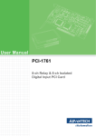
PCI-1763UP
8-Channel Relay & 8-Channel
Isolated Digital Input Low Profile
Card
User Manual
Copyright
The documentation and the software included with this product are copyrighted 2004 by Advantech Co., Ltd. All rights are reserved. Advantech
Co., Ltd. reserves the right to make improvements in the products
described in this manual at any time without notice. No part of this manual may be reproduced, copied, translated or transmitted in any form or
by any means without the prior written permission of Advantech Co., Ltd.
Information provided in this manual is intended to be accurate and reliable. However, Advantech Co., Ltd. assumes no responsibility for its use,
nor for any infringements of the rights of third parties, which may result
from its use.
Acknowledgements
Intel and Pentium are trademarks of Intel Corporation.
Microsoft Windows and MS-DOS are registered trademarks of
Microsoft Corp.
All other product names or trademarks are properties of their respective
owners.
Part No. 2003176300
1st Edition
Printed in Taiwan
Jan 2005
PCI-1763UP User Manual
ii
Product Warranty (2 years)
Advantech warrants to you, the original purchaser, that each of its products will be free from defects in materials and workmanship for two years
from the date of purchase.
This warranty does not apply to any products which have been repaired or
altered by persons other than repair personnel authorized by Advantech,
or which have been subject to misuse, abuse, accident or improper installation. Advantech assumes no liability under the terms of this warranty as
a consequence of such events.
Because of Advantech’s high quality-control standards and rigorous testing, most of our customers never need to use our repair service. If an
Advantech product is defective, it will be repaired or replaced at no
charge during the warranty period. For out-of-warranty repairs, you will
be billed according to the cost of replacement materials, service time and
freight. Please consult your dealer for more details.
If you think you have a defective product, follow these steps:
1.
Collect all the information about the problem encountered. (For
example, CPU speed, Advantech products used, other hardware
and software used, etc.) Note anything abnormal and list any
onscreen messages you get when the problem occurs.
2.
Call your dealer and describe the problem. Please have your manual, product, and any helpful information readily available.
3.
If your product is diagnosed as defective, obtain an RMA (return
merchandize authorization) number from your dealer. This allows
us to process your return more quickly.
4.
Carefully pack the defective product, a fully-completed Repair and
Replacement Order Card and a photocopy proof of purchase date
(such as your sales receipt) in a shippable container. A product
returned without proof of the purchase date is not eligible for warranty service.
5.
Write the RMA number visibly on the outside of the package and
ship it prepaid to your dealer.
iii
CE
This product has passed the CE test for environmental specifications
when shielded cables are used for external wiring. We recommend the use
of shielded cables. This kind of cable is available from Advantech. Please
contact your local supplier for ordering information.
Technical Support and Assistance
Step 1. Visit the Advantech web site at www.advantech.com/support
where you can find the latest information about the product.
Step 2. Contact your distributor, sales representative, or Advantech's customer service center for technical support if you need additional
assistance. Please have the following information ready before
you call:
- Product name and serial number
- Description of your peripheral attachments
- Description of your software (operating system, version, application software, etc.)
- A complete description of the problem
- The exact wording of any error messages
Packing List
Before setting up the system, check that the items listed below are
included and in good condition. If any item does not accord with the
table, please contact your dealer immediately.
1 × PCI-1763UP card
1 × Companion CD-ROM (DLL driver included)
1 × User Manual (this manual)
Safety Precaution - Static Electricity
Follow these simple precautions to protect yourself from harm and the
products from damage.
1.
To avoid electrical shock, always disconnect the power from your
PC chassis before you work on it. Don't touch any components on
the CPU card or other cards while the PC is on.
2.
Disconnect power before making any configuration changes. The
sudden rush of power as you connect a jumper or install a card may
damage sensitive electronic components.
PCI-1763UP User Manual
iv
Contents
Chapter
1 Introduction ......................................................2
1.1
Features ............................................................................. 2
1.1.1
1.1.2
1.1.3
1.1.4
1.1.5
Robust Protection............................................................ 2
Wide Input Range ........................................................... 3
Reset Protection .............................................................. 3
Plug-and-Play Function .................................................. 3
BoardID Switch .............................................................. 3
1.2
1.3
Applications ...................................................................... 4
Installation Guide .............................................................. 4
1.4
Software Overview........................................................... 6
Figure 1.1:Installation Flow Chart.................................. 5
1.4.1
1.4.2
1.5
DLL Driver Programming Roadmap ................................ 7
1.5.1
1.5.2
1.5.3
1.6
Programming Tools ........................................................ 7
Programming with DLL Driver Function Library.......... 8
Troubleshooting DLL Driver Error ................................ 8
Accessories........................................................................ 9
1.6.1
1.6.2
Chapter
DLL Driver ..................................................................... 6
Register-level Programming ........................................... 6
Wiring Cable................................................................... 9
Wiring Boards................................................................. 9
2 Installation ......................................................12
2.1
2.2
Unpacking ....................................................................... 12
Switch and Jumper Settings ............................................ 13
2.2.1
2.3
I/O connectors ................................................................. 15
2.3.1
2.4
Figure 2.1:Card Conn., Jumper & Switch Locations.... 13
Table 2.1:Summary of jumper settings......................... 14
Setting the time to reset the relay outputs..................... 14
Pin Assignments ........................................................... 15
Figure 2.2:I/O Connector Pin Assignments.................. 15
Driver Installation ........................................................... 15
Figure 2.3:Screen of Advantech Automation Software 16
Figure 2.4: Different Options for Driver Setup ............ 17
2.5
Hardware Installation ...................................................... 17
2.6
Device Setup & Configuration........................................ 20
Figure 2.5:Devices Listed on the Device Manager....... 19
2.6.1
2.6.2
Setting Up the Device ................................................... 20
Figure 2.6:The I/O Device Manager Dialog Box ......... 20
Figure 2.7:The "Device(s) Found" Dialog Box ............ 21
Configuring the Device................................................. 21
Figure 2.8:The Device Setting Dialog Box .................. 22
v
Table of Contents
Figure 2.9:The Device Name Appearing on the List of
Devices Box...................................................... 23
Figure 2.10:The Test Dialog Box for Digital Input ...... 24
Figure 2.11:The Test Dialog Box for Digital Output ... 24
Chapter
3 Signal Connections .........................................26
3.1
3.2
Overview ......................................................................... 26
Isolated Digital Input Connections.................................. 26
3.3
Relay Connections........................................................... 27
Figure 3.1:Isolated Digital Input Connections.............. 26
Figure 3.2:Relay Output Connection ............................ 27
Appendix A Specifications ..................................................30
Appendix B Block Diagram ................................................34
Figure B.1:System Block Diagram............................... 34
Appendix C Register Structure and Format.....................36
C.1
C.2
Overview ......................................................................... 36
I/O Port Address Map ..................................................... 36
C.3
Relay I/O Registers - BASE+0H..................................... 38
Table C.1:Register Function ......................................... 37
Table C.2:Register for Relay Output Status ................. 38
Table C.3:Register for Relay Output .......................... 38
C.4
Isolated Digital Input Registers - BASE+1H .................. 39
C.5
Board ID - BASE+2H ..................................................... 39
C.6
Interrupt Status Register - BASE+3H/4H/5H ................. 40
C.7
Interrupt Control Register - BASE+3H/4H/5H............... 41
Table C.4:Register for isolated digital input................. 39
Table C.5:Register for Board ID................................... 39
Table C.6:Register for Interrupt Status......................... 40
Table C.7:Register for Interrupt Control ...................... 41
PCI-1763UP User Manual
vi
CHAPTER
1
Introduction
Sections include:
• Feature
• Application
• Installation Guide
• Software OverView
• DLL Driver Programming Roadmap
• Accessories
Chapter 1 Introduction
Thank you for buying the Advantech PCI-1763UP. The Advantech PCI1763UP is a 8-channel relay actuator and 8-channel isolated digital input
card for the PCI bus.
Its eight on-board SPDT relays are ideal for applications such as device
ON/OFF control or small power switched. For easy monitoring, each
relay is equipped with one red LED to show its ON/OFF status.
The PCI-1763UP's eight optically-isolated digital input channels are ideal
for digital input in noisy environments or with floating potentials.
The following sections of this chapter will provide further information
about features, installation guide, together with some brief information on
software and accessories for the PCI-1763UP card.
1.1 Features
PCI-1763UP offers the following main features:
❏ 8 isolated digital input channels
❏ LED indicators to show activated relays
❏ 8 Form C-type relay output channels
❏ Output status read-back
❏ Keep relay output values when hot system reset
❏ High-voltage isolation on input channels (2,500 VDC)
❏ High ESD protection (2,000 VDC)
❏ High over-voltage protection (70 VDC)
❏ Wide input range (10 ~ 50 VDC)
❏ Interrupt handling capability
❏ BoardID Switch
❏ Low profile
❏ Universal PCI slot, accepts both 3.3 and 5 V
1.1.1 Robust Protection
The PCI-1763UP digital input channels feature a robust isolation protection for industrial, lab and machinery automation applications. It durably
withstands voltage up to 2,500 VDC, preventing your host system from
any incidental harms. If connected to an external input source with surgeprotection, the PCI-1763UP can offer up to a maximum of 2,000 VDC
ESD (Electrostatic Discharge) protection. Even with an input voltage rising up to 70 VDC, the PCI-1763UP can still manage to work properly
albeit only for short period of time.
PCI-1763UP User Manual
2
1.1.2 Wide Input Range
PCI-1763UP has a wide range of input voltage from 10 to 50 VDC, and it
is suitable for most industrial applications with 12 VDC, 24 VDC and 48
VDC input voltage.
1.1.3 Reset Protection
When the system has undergone a hot reset (i.e. without turning off the
system power), the PCI-1763UP can either retain outputs values of each
channel, or return to its default configuration as open status, depending
on its on-board jumper setting. This function protects the system from
wrong operations during unexpected system resets.
1.1.4 Plug-and-Play Function
PCI-1763UP is a Plug-and-Play device, which fully complies with PCI
Specification Rev 2.2. During card installation, there is no need to set
jumpers or DIP switches. Instead, all bus-related configurations such as
base I/O address and interrupt are automatically done by the Plug-andPlay function.
1.1.5 BoardID Switch
PCI-1763UP has a built-in DIP Switch that helps define each card's ID
when multiple PCI-1763UP cards have been installed on the same PC
chassis. The board ID setting function is very useful when users build
their system with multiple PCI-1763UP cards. With correct Board ID settings, you can easily identify and access each card during hardware configuration and software programming.
Note:
✎ For detailed specifications of the PCI-1763UP, please refer to Appendix A, Specifications.
3
Chapter 1
1.2 Applications
❏ Industrial On/Off control
❏ Switch status sensing
❏ Digital I/O control
❏ Industrial and lab automation
❏ SMT/PCB machinery
❏ Semi-conductor machinery
❏ PC-based Industrial Machinery
❏ Testing & Measurement
❏ Laboratory & Education
❏ External relay driving
1.3 Installation Guide
Before you install your PCI-1763UP card, please make sure you have the
following necessary components:
❏ PCI-1763UP card
❏ PCI-1763UP User's Manual
❏ Driver software
Advantech DLL drivers (included in the
companion CD-ROM
❏ Wiring cable
PCL-10144 (optional)
❏ Wiring board
ADAM-3944 (optional)
❏ Computer
Personal computer or workstation with a
PCI-bus slot (running Windows 98/
2000/XP)
Some other optional components are also available for enhanced operation:
❏ Application software
ActiveDAQ, ADAQ-VIEW or other
third-party software packages
After you get the necessary components and maybe some of the accessories for enhanced operation of your DAS card, you can then begin the
Installation procedures. Figure 1-1 provides a concise flow chart to give
users a broad picture of the software and hardware installation procedures.
PCI-1763UP User Manual
4
Figure 1.1: Installation Flow Chart
5
Chapter 1
1.4 Software Overview
Advantech offers a rich set of DLL drivers, third-party driver support and
application software to help fully exploit the functions of your PCI1763UP card:
! DLL driver (on the companion CD-ROM)
! LabVIEW driver
! Advantech ActiveDAQ
! Advantech ADAQ-VIEW
Programming choices for DA&C cards: You may use Advantech application software such as Advantech DLL driver. On the other hand,
advanced users are allowed another option for register-level programming, although not recommended due to its laborious and time-consuming nature.
1.4.1 DLL Driver
The Advantech DLL Drivers software is included on the companion CDROM at no extra charge. It also comes with all the Advantech DA&C
cards. Advantech's DLL driver features a complete I/O function library to
help boost your application performance. The Advantech DLL driver for
Windows 98/2000/XP works seamlessly with development tools such as
Visual C++, Visual Basic, Borland C++ Builder and Borland Delphi.
1.4.2 Register-level Programming
Register-level programming is reserved for experienced programmers
who find it necessary to write codes directly at the level of device registers. Since register-level programming requires much effort and time, we
recommend that you use the Advantech DLL drivers instead. However, if
register-level programming is indispensable, you should refer to the relevant information in Appendix C, Register Structure and Format, or to the
example codes included on the companion CD-ROM.
PCI-1763UP User Manual
6
1.5 DLL Driver Programming Roadmap
This section will provide you a roadmap to demonstrate how to build an
application from scratch using Advantech DLL driver with your favorite
development tools such as Visual C++, Visual Basic, Delphi and C++
Builder. The step-by-step instructions on how to build your own applications using each development tool will be given in the DLL Drivers Manual. Moreover, a rich set of example source codes are also given for your
reference.
1.5.1 Programming Tools
Programmers can develop application programs with their favorite development tools:
❏ Visual C++
❏ Visual Basic
❏ Delphi
❏ C++ Builder
For instructions on how to begin programming works in each development tool, Advantech offers a Tutorial Chapter in the DLL Drivers Manual for your reference. Please refer to the corresponding sections in this
chapter on the DLL Drivers Manual to begin your programming efforts.
You can also take a look at the example source codes provided for each
programming tool, since they can get you very well-oriented.
The DLL Drivers Manual can be found on the companion CD-ROM. Or
if you have already installed the DLL Drivers on your system, The DLL
Drivers Manual can be readily accessed through the Start
button:
Start\Programs\Advantech Automation\Device Manager\Device
Driver’s Manual
The example source codes could be found under the corresponding installation folder such as the default installation path:
\Program Files\Advantech\ADSAPI\Examples
For information about using other function groups or other development
tools, please refer to the Creating Windows 98/2000/XP Application with
DLL Driver chapter and the Function Overview chapter in the DLL Drivers Manual.
7
Chapter 1
1.5.2 Programming with DLL Driver Function Library
Advantech DLL driver offers a rich function library to be utilized in various application programs. This function library consists of numerous
APIs that support many development tools, such as Visual C++, Visual
Basic, Delphi and C++ Builder.
According to their specific functions or services, those APIs can be categorized into several function groups:
❏ Digital Input/Output Function Group
❏ Counter Function Group
❏ Port Function Group (direct I/O)
❏ Event Function Group
For the usage and parameters of each function, please refer to the Function Overview chapter in the DLL Drivers Manual.
1.5.3 Troubleshooting DLL Driver Error
Driver functions will return a status code when they are called to perform
a certain task for the application. When a function returns a code that is
not zero, it means the function has failed to perform its designated function. To troubleshoot the DLL driver error, you can pass the error code to
DRV_GetErrorMessage function to return the error message. Or you
can refer to the DLL Driver Error Codes Appendix in the DLL Drivers
Manual for a detailed listing of the Error Code, Error ID and the Error
Message.
PCI-1763UP User Manual
8
1.6 Accessories
Advantech offers a complete set of accessory products to support the PCI1763UP card. These accessories include:
1.6.1 Wiring Cable
" PCL-10144
The PCL-10144 shielded cable is specially designed
for PCI-1763UP cards to provide high resistance to
noise. To achieve a better signal quality, the signal
wires are twisted in such a way as to form a "twistedpair cable", reducing cross-talk and noise from other
signal sources. Furthermore, its analog and digital
lines are separately sheathed and shielded to neutral
ize EMI/EMC problems.
1.6.2 Wiring Boards
❏ ADAM-3944
The ADAM-3944 is a 44-pin D-type wiring terminal
module for DIN-rail mounting. This terminal module
can be readily connected to the Advantech PC-Lab
cards and allow easy yet reliable access to individual
pin connections for the PCI-1763UP card.
9
Chapter 1
PCI-1763UP User Manual
10
CHAPTER
2
Installation
Sections include:
• Unpacking
• Switch and Jumper Setting
• I/O connectors
• Driver Installation
• Hardware Installation
• Device Setup & Configuration
Chapter 2 Installation
This chapter has a package item checklist, proper instructions about
unpacking and step-by-step procedures for both driver and card installation.
2.1 Unpacking
After receiving your PCI-1763UP package, please inspect ita contents
first. The package should contain the following items:
! PCI-1763UP card
! Companion CD-ROM (DLL driver included)
! User's Manual
The PCI-1763UP card harbors certain electronic components vulnerable
to electrostatic discharge (ESD). ESD could easily damage the integrated
circuits and certain components if preventive measures are not carefully
paid attention to.
Before removing the card from the antistatic plastic bag, you should
take the following precautions to ward off possible ESD damage:
! Touch the metal part of your computer chassis with your hand to dis
charge static electricity accumulated on your body. Or one can also
use a grounding strap.
! Touch the anti-static bag to a metal part of your computer chassis
before opening the bag.
! Take hold of the card only by the metal bracket when removing it out
of the bag.
After taking out the card, you should first:
! Inspect the card for any possible signs of external damage (loose or
damaged components, etc.). If the card is visibly damaged, please
notify our service department or our local sales representative
immediately. Avoid installing a damaged card into your system.
PCI-1763UP User Manual
12
Also pay extra caution to the following aspects to ensure proper installation:
! Avoid physical contact with materials that could hold static electric
ity such as plastic, vinyl and Styrofoam.
! Whenever you handle the card, grasp it only by its edges. DO NOT
TOUCH the exposed metal pins of the connector or the electronic
components.
Note:
✎ Keep the anti-static bag for future use. You might need the original
bag to store the card if you have to remove the card from PC or trans
port it elsewhere.
2.2 Switch and Jumper Settings
The PCI-1763UP card has one function switch settings.
Figure 2.1: Card Connectors, Jumper & Switch Locations
13
Chapter 2
Table 2.1: Summary of jumper settings
Names of Jumpers
Function description
Keep last status after hot
reset
JP2
Default configuration
2.2.1 Setting the time to reset the relay outputs
Some users will want the capability of clearing each relay output when
the system (or PC) issues a reset signal on the PCI bus. Some users will
want to clear their relays only as part of system power-on. The PCI1763UP satisfies both these needs by providing jumper JP2. Depending
on the application, this capability may allow relay outputs to be "OFF"
without requiring a complete shutdown of processes controlled by the
card.
PCI-1763UP User Manual
14
2.3 I/O connectors
2.3.1 Pin Assignments
Figure 2-2 shows the pin assignments for the 44-pin I/O connector on
PCI-1763UP
DInL:
Digital Input Low, Channel n
DInH:
Digital Input High, Channel n
NC n:
Normal close pin of relay n
NO n:
Normal open pin of relay n
COM n:
Common pin of relay n
Figure 2.2: I/O Connector Pin Assignments
2.4 Driver Installation
Note:
✎ We recommend you to install the driver before you install the PCI1763UP card into your system, since this will guarantee a smooth
installation process.
The 32-bit DLL driver Setup program for the PCI-1763UP card is
included on the companion CD-ROM that is shipped with your DA&C
card package. Please follow the steps below to install the driver software:
Step 1: Insert the companion CD-ROM into your CD-ROM drive.
15
Chapter 2
Step 2: The Setup program will be launched automatically if you have
the autoplay function enabled on your system. When the Setup
Program is launched, you'll see the following Setup Screen.
Note:
✎ If the autoplay function is not enabled on your computer, use Win
dows Explorer or Windows Run command to execute Autorun.exe
on the companion CD-ROM.
Figure 2.3: Screen of Advantech Automation Software
Step 3: Select the individual driver.
Step 4: Follow the installation instructions step by step to complete your
DLL driver setup.
PCI-1763UP User Manual
16
Figure 2.4: Different Options for Driver Setup
For further information on driver-related issues, an online version of DLL
Drivers Manual is available by accessing the following path:
Start\Programs\Advantech Automation\Device Manager\Device
Driver’s Manual
2.5 Hardware Installation
Note:
✎ Make sure you have installed the driver first before you install the
card (please refer to 2.4 Driver Installation)
After the DLL driver installation is completed, you can now go on to
install the PCI-1763UP card in any PCI slot on your computer. But it is
suggested that you should refer to the computer user manual or related
documentation if you have any doubt. Please follow the steps below to
install the card on your system.
Step 1: Turn off your computer and unplug the power cord and cables.
TURN OFF your computer before installing or removing any
components on the computer.
Step 2: Remove the cover of your computer.
17
Chapter 2
Step 3: Remove the slot cover on the back panel of your computer.
Step 4: Touch the metal part on the surface of your computer to neutral
ize the static electricity that might be on your body.
Step 5: Insert the PCI-1763UP card into a PCI slot. Hold the card only by
its edges and carefully align it with the slot. Insert the card firmly
into place. Use of excessive force must be avoided, otherwise the
card might be damaged.
Step 6: Fasten the bracket of the PCI card on the back panel rail of the
computer with screws.
Step 7: Connect appropriate accessories (44-pin cable, wiring terminals,
etc. if necessary) to the PCI card.
Step 8: Replace the cover of your computer chassis. Re-connect the
cables you removed in step 2.
Step 9: Plug in the power cord and turn on the computer .
Note:
✎ In case you installed the card without installing the DLL driver first,
Windows 98 will recognize your card as an "unknown device"
after rebooting, and will prompt you to provide the necessary driver.
You should ignore the prompting messages (just click the Cancel
button) and set up the driver according to the steps described in 2.4
Driver Installation.
After the PCI-1763UP card is installed, you can verify whether it is properly installed on your system in the Device Manager:
1. Access the Device Manager through Control Panel/System/Device
Manager.
2. The device name of the PCI-1763UP should be listed on the Device
Manager tab on the System Property Page.
PCI-1763UP User Manual
18
Figure 2.5: Devices Listed on the Device Manager
Note:
✎ If your card is properly installed, you should see the device name of
your card listed on the Device Manager tab. If you do see your
device name listed on it but marked with an exclamation sign
"!", it means your card has not been correctly installed. In this
case, remove the card device from the Device Manager by select
ing its device name and press the Remove button. Then go
through the driver installation process again.
After your card is properly installed on your system, you can now configure your device using the Device Manager Program that has itself already
been installed on your system during driver setup. A complete Device
Manager procedure should include device setup, configuration and testing. The following sections will guide you through the Setup, Configuration and Testing of your device.
19
Chapter 2
2.6 Device Setup & Configuration
The Device Manager program is a utility that allows you to set up, configure and test your device, and later stores your settings on the system
registry. These settings will be used when you call the APIs of Advantech
32-bit DLL drivers.
2.6.1 Setting Up the Device
Step 1: To install the I/O device for your card, you must first run the
Device Manager program (by accessing Start/Programs/
Advantech Automation/Device Manager/
Step 2: On the Device Manager program window, you can see the I/O
Device Manager dialog box (Fig. 2-6).
You can then view the device(s) already installed on your system
(if any) on the supported Devices list box.
Figure 2.6: The I/O Device Manager Dialog Box
Step 3: Scroll down the List of Devices box to find the device that you
wish to install, then click the Add… button to evoke the Device(s)
PCI-1763UP User Manual
20
found dialog box such as one shown in Fig. 2-7. The Device(s)
found dialog box lists all the installed devices on your system.
Select the device you want to configure from the list box and
press the OK button. After you have clicked OK, you will see a
Device Setting dialog box such as the one in Fig. 2-7.
Figure 2.7: The "Device(s) Found" Dialog Box
2.6.2 Configuring the Device
Step 4: On the Device Setting dialog box (Fig. 2-8), you can configure
the ID0 ~ ID7 Interrupt trigger mode either as Rising Edge or
Falling Edge, and Enable or Disable the ID0 ~ ID7.
21
Chapter 2
Figure 2.8: The Device Setting Dialog Box
Step 5: After you have finished configuring the device, click OK and the
device name will appear in the Installed Devices box as seen
in Fig. 2.9
PCI-1763UP User Manual
22
Figure 2.9: The Device Name Appearing on the List of Devices Box
Note:
✎ As we have noted, the device name
“000:<PCI-1763UP BoardID = 12 I/O = b800H >”
begins with a device number "000", which is specifically assigned to
each card. The device number is passed to the driver to specify
which device you wish to control.
After your card is properly installed and configured, you can click the
Test… button to test your hardware by using the testing utility we supplied. For more detailed information, please refer to the DLL Drivers
Manual.
23
Chapter 2
Figure 2.10: The Test Dialog Box for Digital Input
Figure 2.11: The Test Dialog Box for Digital Output
You can also find the useful examples on the CD-ROM to speed up your
programming.
PCI-1763UP User Manual
24
CHAPTER
3
Signal Connections
Sections include:
• Overview
• Isolated Digital Input Connections
• Relay Connections
Chapter 3 Signal Connections
3.1 Overview
Maintaining signal connections is one of the most important factors in
ensuring that your application system is sending and receiving data correctly. A good signal connection can avoid unnecessary and costly damage to your PC and other hardware devices. This chapter provides useful
information about how to connect input and output signals to the PCI1763UP via the I/O connector.
3.2 Isolated Digital Input Connections
The PCI-1763UP has 8 isolated digital input channels designated
DI0~DI7.
Each of isolated digital input channel accepts 10~50 VDC voltage
inputs, and accept bi-directional input. It means that you can apply
positive or negative voltage to an isolated input pin (Vin ). The figure
below shows how to connect an external input source to one of the
card's isolated input channels
Figure 3.1: Isolated Digital Input Connections
PCI-1763UP User Manual
26
3.3 Relay Connections
After power on, the initial relay output status of PCI-1763UP is shown as
below:
Figure 3.2: Relay Output Connection
A write operation to I/O address, BASE +0, will change the output
status of each relay. For example, if Bit 0 of BASE +0 is set "1" (logic
high), relay 0, K0, will switch from position "NORMALLY CLOSED",
R0_NC, to position "NORMALLY OPEN", R0_NO. This means that
LOAD2 will be de-energized, while LOAD1 is energized.
To summarize, the "COMMON" line connect to the "NORMALLY
CLOSED" line, if the corresponding bit is set as 0 (power-on initial
status). Otherwise, if the corresponding bit is set as 1, then the
"COMMON" line will connect to the "NORMALLY OPEN" line.
27
Chapter 3
PCI-1763UP User Manual
28
APPENDIX
A
Specifications
Appendix A Specifications
Table 1: Isolated Digital Input
Number of Input Channels
8
Optical Isolation
Opto-isolator response
time
Over-voltage Protect
2500 V DC
25 µs
70 VDC
Input Voltage
Input Current
VIH (max.)
50 VDC
VIH (min.)
5 VDC
VIL (max.)
3 VDC
10 VDC
3.16mA (typical)
15 VDC
4.94 mA (typical)
24 VDC
8.13 mA (typical)
48 VDC
16.6 mA (typical)
50 VDC
17.3 mA (typical)
Table 2: Relay Output
Number of Output Channels
8
Relay Type
DPDT (8 Form C)
Rating (resistive)
0.25 A* 240 VAC or 1 A* 30 VDC
Max. Switching Power
62.5 AV, 60 W
Max. Switching Voltage
250 VAC, 220 VDC
Max. Switching Current
5A
Operate time
5 ms max.
Release time
4 ms max.
Insulation Resistance
>1X10e9 . (at 500 VDC)1,000 M min. (at 500 VDC)
Life Expectancy
PCI-1763UP User Manual
Mechanical
1X10e8 ops. min.
Electrical
2x10 e5 ops. min.(contact rating)
30
Table 3: General
I/O Connector Type
Dimensions
Power Consumption
44-pin D-type female
120 x 64.4 mm (4.7" x 2.5")
+5V @ 107.5 mA (typical)
+5V @ 301.3 mA (max.)
Operating
Temperature
Storage
Relative Humidity
0 ~ 60 °C (32 ~ 140°F)
(refer to IEC 68-2-1,2)
-20 ~ 70 °C (-4 ~158 °F)
5 - 95 % RH non-condensing
(refer to IEC 68-2-3)
Certification
CE Class A certified
31
Appendix A
PCI-1763UP User Manual
32
APPENDIX
B
Block Diagram
Appendix B Block Diagram
Figure B.1: System Block Diagram
PCI-1763UP User Manual
34
APPENDIX
C
Register Structure and
Format
Appendix C Register Structure and Format
C.1 Overview
The PCI-1763UP is delivered with an easy-to-use 32-bit DLL driver for
user programming under the Windows 98/2000/XP operating system. We
advise users to program the PCI-1763UP using the 32-bit DLL driver
provided by Advantech to avoid the complexity of low-level programming by register.
The most important consideration in programming the PCI-1763UP the
register level is to understand the function of the card's registers. The
information in the following sections is provided only for users who
would like to do their own low-level programming.
C.2 I/O Port Address Map
The PCI-1763UP requires 32 consecutive addresses in the PC's I/O space.
The address of each register is specified as an offset from the card's base
address. For example, BASE+0 is the card's base address and BASE+7 is
the base address plus seven bytes.
Table C-1 shows the function of each register of the PCI-1763UP or
driver and its address relative to the card's base address.
PCI-1763UP User Manual
36
Table C.1: Register Function
Base Addr,
+ Hex
R
0H
W
R
1H
7
6
5
4
RS7
RS6
RS5
RS4
RO7
RO6
RO5
IDI7
IDI
5H
RS1
RS0
RO3
RO2
RO1
RO0
IDI5
IDI4
IDI3
IDI1
IDI0
BD1
BD0
IDI1EN
IDI0EN
IDI1EN
IDI0EN
IDI1RF
IDI0RF
IDI2RF
IDI1RF
IDI0RF
IDI2F
IDI1F
IDI0F
IDI1CLR
IDI0CLR
IDI2
Board ID Register
BD3
BD2
N/A
Interrupt Enable Status
IDI7EN
IDI6EN
IDI5EN
IDI4EN
IDI3EN
IDI2EN
Interrupt Enable Register
IDI7EN
R
RS2
N/A
W
W
0
Isolated Digital Input
W
4H
RS3
RO4
2H
R
1
Relay Output
R
3H
2
Relay Output Status
W
R
3
IDI6EN
IDI5EN
IDI4EN
IDI3EN
IDI2EN
Interrupt Triggering Status
IDI7RF
IDI6RF
IDI5RF
IDI4RF
IDI3RF
IDI2RF
Interrupt Triggering Register
IDI7RF
IDI6RF
IDI5RF
IDI4RF
IDI3RF
Interrupt Flag
IDI7F
IDI6F
IDI5F
IDI4F
IDI3F
Interrupt Clear Register
W
IDI7CLR
IDI6CLR
IDI5CLR
IDI4CLR
37
IDI3CLR
IDI2CLR
Appendix C
C.3 Relay I/O Registers - BASE+0H
The PCI-1763UP offers 8-ch relay actuators. These I/O channels use the
input and output ports at addresses BASE+0H.
Table C.2: Register for Relay Output Status
Read
Bit #
BASE +0H
Relay Output Status
7
6
5
4
3
2
1
0
RS7
RS6
RS5
RS4
RS3
RS2
RS1
RS0
Table C.3: Register for Relay Output
Write
Bit #
BASE +0H
Relay Output
7
6
5
4
3
2
1
0
RO7
RO6
RO5
RO4
RO3
RO2
RO1
RO0
Note:
✎ The default configuration of the digital output channels is a logic 0.
This avoids damaging external devices during system start-up or
reset since the power on status is set to the default value.
PCI-1763UP User Manual
38
C.4 Isolated Digital Input Registers - BASE+1H
The PCI-1763UP offers 8-ch isolated digital input channels. These channels use the input ports at addresses BASE+1H.
Table C.4: Register for isolated digital input
Read
Bit #
BASE +1H
Isolated Digital Input
7
6
5
4
3
2
1
0
IDI7
IDI6
IDI5
IDI4
IDI3
IDI2
IDI1
IDI0
C.5 Board ID - BASE+2H
The PCI-1763UP offers Board ID register BASE+2H. With correct
Board ID settings, user can easily identify and access each card during
hardware configuration and software programming.
Table C.5: Register for Board ID
Read
Bit #
Board ID
7
6
5
4
BASE +2H
BD3 ~ DB0
3
2
1
0
BD3
BD2
BD1
BD0
Board ID
BD0 LSB of the Board ID
BD3 MSB of the Board ID
39
Appendix C
C.6 Interrupt Status Register - BASE+3H/4H/5H
The Interrupt Status Register control the status of eight interrupt signal
sources (IDI0 ~ IDI7).
Table C.6: Register for Interrupt Status
Read
Bit #
Interrupt Status Register
7
6
5
4
3
2
1
0
BASE +3H
IDI7EN
IDI6EN
IDI5EN
IDI4EN
IDI3EN
IDI2EN
IDI1EN
IDI0EN
BASE +4H
IDI7RF
IDI6RF
IDI5RF
IDI4RF
IDI3RF
IDI2RF
IDI1RF
IDI0RF
BASE +5H
IDI7F
IDI6F
IDI5F
IDI4F
IDI3F
IDI2F
IDI1F
IDI0F
IDInF
Interrupt flag bits (n = 0 ~ 7)
This bit is a flag indicating the status of an interrupt.
User can read this bit to get the status of the interrupt
0 No interrupt
1 Interrupt occurred
IDInRF
Interrupt enable control bits (n = 0 ~ 7)
Read this bit to Enable/Disable the interrupt.
0 Disable
1 Enable
IDInEN
Interrupt triggering control bits (n = 0 ~ 7)
The interrupt can be triggered by a rising edge or
falling edge of the interrupt signal, as determined by
the value in this bit.
0 Rising edge trigger
1 Falling edge trigger
PCI-1763UP User Manual
40
C.7 Interrupt Control Register - BASE+3H/4H/5H
The Interrupt Control Register control the status of two interrupt signal
sources (IDI0 ~ IDI7). The user can clear the interrupt by writing its corresponding value to the Interrupt Control Register, as shown in below
table.
Table C.7: Register for Interrupt Control
Write
Interrupt Control Register
7
6
5
4
3
2
1
0
BASE +3H
IDI7EN
IDI6EN
IDI5EN
IDI4EN
IDI3EN
IDI2EN
IDI1EN
IDI0EN
BASE +4H
IDI7RF
IDI6RF
IDI5RF
IDI4RF
IDI3RF
IDI2RF
IDI1RF
IDI0RF
BASE +5H
IDI7CLR
IDI6CLR
IDI5CLR
IDI4CLR
IDI3CLR
IDI2CLR
IDI1CLR
IDI0CLR
Bit #
IDInCLR
Interrupt clear control bits (n = 0 ~ 7)
This bit must first be cleared to service the next inter
rupt.
0 Ignore
1 Clear the interrupt
IDInRF
Interrupt enable control bits (n = 0 ~ 7)
Read this bit to Enable/Disable the interrupt.
0 Disable
1 Enable
IDInEN
Interrupt triggering control bits (n = 0 ~ 7)
The interrupt can be triggered by a rising edge or
falling edge of the interrupt signal, as determined by
the value in this bit.
0 Rising edge trigger
1 Falling edge trigger
41
Appendix C
PCI-1763UP User Manual
42