1
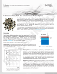
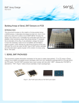
J-Series High-Density Fill Factor Silicon Photomultipliers
IN
A
R
Y
USER MANUAL
High-Density Fill Factor Silicon Photomultipliers
SensL’s J-Series low-light sensors feature an industry-leading low dark count rate and a high PDE that extends
much further into the blue part of the spectrum using a high-volume, P-on-N silicon process. Improvements have
been made to both the standard (anode-cathode) rise time and the recovery time, in addition to the inclusion of
SensL’s unique fast output that offers sub-nanosecond pulse widths. J-Series sensors are available in different sizes
(3mm and 6mm) and use TSV (Through Silicon Via) technology to create a CSP (Chip Scale Package) with minimal
deadspace, that is compatible with industry standard, lead-free, reflow soldering processes.
The J-Series Silicon Photomultipliers (SiPM) form a range of high gain,
single-photon sensitive, UV-to-visible light sensors. They have performance
characteristics similar to a conventional PMT, while benefiting from the
practical advantages of solid-state technology: low operating voltage,
excellent temperature stability, robustness, compactness, output uniformity,
and low cost. For more information on the J-Series sensors please refer to
the datasheet.
Overview
M
J-Series
J-Series SiPM sensors from SensL are based on a P-on-N diode structure
(Figure 1), which provides optimized PDE at the blue end of the visible
spectrum, and feature a number of significant performance upgrades:
P
R
E
LI
PDE: J-Series sensors feature increased microcell density, giving an overall
improvement to PDE (with a peak at >50%), along with other optimizations
that extend the sensitivity into the UV, (>5% PDE at 250nm). This PDE
improvement is achieved while keeping the dark count rate <100kHz/mm2.
Figure 1, P-on-N sensor structure
Timing: J-Series sensors feature reduced microcell recovery time
and standard signal rise time. All J-Series sensors also feature
SensL’s proprietary fast output terminal (Figure 2), which is the
derivative of the internal fast switching of the microcell in response
to the detection of a single photon, which has sub-nanosecond
rise times and pulse-widths.
Package: J-Series sensors are available as either a 3mm or 6mm
chip packaged using a TSV (through-silicon via) process to create
a CSP (Chip Scale Package) with minimal deadspace. The TSV
sensors have a number of ball contacts on the reverse, giving
access to the fast output as well as the anode and cathode.
Figure 2, Simplified microcell level schematic of
the J-Series SiPM.
SensL © 2015
1
J-Series High-Density Fill Factor Silicon Photomultipliers
USER MANUAL
Contents
Overview.............................................................................................................................................................1
IN
A
R
Y
Biasing and Readout...........................................................................................................................................3
Recommended Biasing................................................................................................................................3
Recommended Readout and Amplification...................................................................................................3
Readout of the Fast Output..........................................................................................................................3
J-Series Mounted Sensors..................................................................................................................................4
MicroFJ-SMA...............................................................................................................................................4
MicroFJ-SMTPA...........................................................................................................................................5
Handling and Soldering.......................................................................................................................................6
Safe Handling of Sensors.............................................................................................................................6
Product Packaging.......................................................................................................................................6
Cleaning.......................................................................................................................................................6
M
Solder Reflow Conditions.............................................................................................................................7
Package Drawings (All Dimensions in mm)...........................................................................................................8
MicroFJ-300XX-TSV Package & Solder Footprint.........................................................................................8
LI
MicroFJ-60035-TSV Package & Solder Footprint.........................................................................................9
MicroFJ-SMA-60035.................................................................................................................................10
MicroFJ-SMTPA-60035.............................................................................................................................11
R
E
Further Help......................................................................................................................................................12
P
Appendix A - Biasing Alternatives & Signal Polarity............................................................................................13
SensL © 2015
2
USER MANUAL
Biasing and Readout
Recommended Biasing
IN
A
R
Y
The cathode needs to be held at a positive bias with respect to the anode, as in Figure 3. It is recommended that
bias voltage decoupling, such as the examples shown in Figure 4, is used to provide a stable operating condition.
Please refer to the Appendix for further information on biasing schemes and the resulting signal polarities.
Figure 3, Recommended biasing
Figure 4, Generic biasing set-up with decoupling capacitors.
Recommended Readout and Amplification
R
E
LI
M
Figure 5 shows how the J-Series sensors can be connected to a standard high-speed amplifier, such as the
OPA656, to convert the standard output signal current to a voltage. This particular arrangement is suitable for
either the 3mm or 6mm sensors.
Figure 5, Example circuit for readout of individual sensors.
P
Y
J-Series High-Density Fill Factor Silicon Photomultipliers
Readout of the Fast Output
For extensive information about the fast output and its readout, please consult pages 4-8 of the C-Series User
Manual. In addition, Appendix A of this document shows the resulting signal polarities when various biasing
schemes are used.
SensL © 2015
3
J-Series High-Density Fill Factor Silicon Photomultipliers
USER MANUAL
J-Series Mounted Sensors
MicroFJ-SMA
IN
A
R
Y
J-Series sensors are available ready-mounted on test boards, to allow for easy evaluation. The MicroFJ-SMA-XXXXX
sensors (Figure 6) feature the TSV-packaged SiPM sensor reflow-soldered onto a small PCB. The board is simple to
use, having just three SMA (female) connectors: one delivers the bias voltage (Vbias) and the other two provide the
output signals: standard output from the anode (Sout) and the fast output (Fout). The SMA board requires a positive
bias, which allows the standard output to be referenced to ground rather than the bias. For the complete circuit
schematic, please consult the TSV Board Reference Design document.
Bias
TSV
sensor
Fast
output
Standard
output
M
Mounting
holes
LI
Figure 6, The MicroFJ-SMA-300XX board.
Output
Vbias
Fout
Standard female
SMA connector
R
E
Sout
Connector
Function
bias input (cathode)
Comments
positive bias input
fast output
if unused can be left open
standard output (anode)
if unused can be left open
Table 1, SMA Connections
P
The MicroFJ-SMA board is for users who require a plug-and-play set-up to quickly evaluate the TSV sensors with
optimal timing performance. The board provides outputs which can be connected directly to the oscilloscope or
measurement device. The board also allows the standard output from the anode to be observed at the same time
as the fast output. Table 1 summarizes the connections to the SMA board. Each board has two mounting holes to
allow secure placement during testing.
For more discussion regarding the readout of the fast output signals, please consult pages 4-8 of the C-Series User
Manual. In addition Appendix A of this document shows the signal output polarities when various biasing schemes
are used.
SensL © 2015
4
USER MANUAL
MicroFJ-SMTPA
Pin
No.
Connection
1
IN
A
R
Y
The MicroFJ-SMTPA-XXXXX, or Pin Adapter board (Figure 7), features a TSV-packaged J-Series sensor (type
specified by the XXXXX digits) mounted onto a small PCB board. The PCB has five through-hole pins that allow easy
electrical connections to the electrodes of the TSV sensor. The pins are labeled on the PCB with numbers 1 - 5. Each
of the numbered pins is connected as listed in Table 2, with the option to use either a positive or negative bias. For
the complete circuit schematic, please consult the TSV Board Reference Design document.
Function
Positive bias
Negative bias
anode
standard output
(if unused connect to zero V)
negative bias input
2
fast
fast output
(if unused can be left open)
fast output
(if unused can be left open)
3
cathode
positive bias input
standard output
(if unused connect to zero V)
4
gnd
PCB gnd
PCB gnd
5
n/c
do not connect
do not connect
M
Table 2, Pin assignments for the MicroFC-SMTPA board
The does not include any on-board decoupling on the bias line. Therefore, bias decoupling, such as that in Figure 4,
should be included on the bias line at the relevant pin (see Table 2). The standard output can be connected directly
to an amplifier or 50W load oscilloscope. If the standard output is not used, then that pin should be connected to
zero Volts.
LI
Due to the presence of the pins on the SMTPA board, it is not optimal for evaluation testing where timing with the
fast output signal is critical. For evaluations where the timing performance of the fast output is critical, the use of the
SMA board is recommended.
The connectors from Samtec used are:
R
E
BBL-103-G-E
BBL-102-G-E
Compatible sockets from Samtec are:
SL-103-G-10
SL-102-G-10
Figure 7, The top and bottom of the MicroFJSMTPA-60035 board showing the through-hole pins.
P
Y
J-Series High-Density Fill Factor Silicon Photomultipliers
For more discussion regarding the readout of the fast output signals, please consult pages 4-8 of the C-Series
User Manual. In addition Appendix A of this document shows the signal output polarities when various biasing
schemes are used.
SensL © 2015
5
J-Series High-Density Fill Factor Silicon Photomultipliers
USER MANUAL
Safe Handling of Sensors
R
Y
Handling and Soldering
• When unpacking, care should be taken to prevent dropping or misorienting the sensors. The specific items
contained in the package and the type of packaging will depend on the parts ordered.
• Remember that the SiPM is a sensitive optoelectronic instrument; always handle the sensor as carefully as
possible.
IN
A
• The sensor should be disconnected from the bias supply when not in use.
• SiPM sensors are ESD sensitive. The following precautions are recommended:
• Ensure that personal grounding, environmental controls and work surfaces are compliant with
recommendations in JESD625.
• Ensure that all personnel handling these devices are trained according to the recommendations in
JESD625.
• Devices must be placed in an ESD approved carrier during transport through an uncontrolled area.
M
• Complete handling information can be found in the TSV Handling and Soldering guide.
LI
Product Packaging
E
The sensors are shipped in moisture barrier bags (MBBs) according to J-STD 033 standard. An unopened MBB
should be stored at a temperature below 40OC and relative humidity <90%. After the MBB has been opened, the
devices must be reflow soldered within a period of time depending on the moisture sensitivity level (MSL), which is
MSL3. See Table 3 for details.
Exposure time
Condition
3
168 hours
≤30 °C/60% RH
R
MSL
Table 3, MSL definitions applicable to the J-Series sensors (reference J-STD 020).
P
Cleaning
The parts can be cleaned using Isopropyl alcohol.
SensL © 2015
6
USER MANUAL
Solder Reflow Conditions
IN
A
R
Y
The J-Series sensors must be mounted according to specified soldering pad patterns as given on pages 8 and 9.
The ‘No Connect’ pins are electrically isolated and should be soldered to a ground (or bias) plane to help with heat
dissipation.
Solder paste must be evenly applied to each soldering pad to insure proper bonding and positioning of the
component. After soldering, allow at least three minutes for the component to cool to room temperature before
further operations.
Solder reflow conditions must be in compliance with J-STD-20, table 5.2. This is summarized in Figure 8. The
number of passes shall not be more than 2.
Complete soldering information can be found in the TSV Handling and Soldering guide.
Solder Reflow Profile
300
Max 260OC
Max 4OC/sec
200
217OC
180OC
150
60~100sec
60 to 120 sec
M
Temperature (OC)
250
Max 10sec at 260OC
100
50
LI
0
0
50
100
150
200
250
300
Time (sec)
R
E
Figure 8, Reflow solder profile for use with J-Series sensors.
P
Y
J-Series High-Density Fill Factor Silicon Photomultipliers
SensL © 2015
7
J-Series High-Density Fill Factor Silicon Photomultipliers
USER MANUAL
Package Drawings (All Dimensions in mm)
M
IN
A
R
Y
MicroFJ-300XX-TSV Package & Solder Footprint
Pin #
J-Series
B1
Anode
B3
Fast Output
A1, C3
Cathode
All others
No Connect *
* The ‘No Connect’ pins are electrically
isolated and should be soldered to a
ground (or bias) plane to help with heat
dissipation.
P
R
E
LI
The complete MicroFJ-300XX-TSV CAD can be downloaded from the
website, here.
Pin Assignments
Solder footprint (all dimensions in mm)
SensL © 2015
8
J-Series High-Density Fill Factor Silicon Photomultipliers
USER MANUAL
R
Y
LI
M
IN
A
Y
MicroFJ-60035-TSV Package & Solder Footprint
6.13
MicroFJ-60035-TSV
C1, D1
Anode
A1, F6
Cathode
C6, D6
Fast Output
All others
No Connect *
* The ‘No Connect’ pins are electrically isolated and should be soldered to a ground (or
bias) plane to help with heat dissipation.
1
P
0.4
7
6.13
0.
27
R
0.565
E
The complete MicroFJ-60035-TSV CAD can be downloaded from the
website, here.
Ball Assignments
Ball #
0.565
1
Solder footprint (all dimensions in mm)
SensL © 2015
9
J-Series High-Density Fill Factor Silicon Photomultipliers
USER MANUAL
R
E
LI
M
IN
A
R
Y
MicroFJ-SMA-60035
SND0150
MicroFJ-SMA-60035-TSV
SND0150
P
MicroFJ-SMA-60035-TSV
Full CAD schematics are available to download,
for both the 3mm and 6mm versions of the SMA board.
SensL © 2015
10
J-Series High-Density Fill Factor Silicon Photomultipliers
USER MANUAL
IN
A
R
Y
Y
MicroFJ-SMTPA-60035
R
E
LI
M
Detector
Detector
Detector
P
etector
Full CAD schematics are available to download, for both the 3mm and 6mm versions of the SMTPA board.
Pin Assignments
SensL © 2015
Pin #
1
2
Function
Anode
Fast Output
11
J-Series High-Density Fill Factor Silicon Photomultipliers
USER MANUAL
Further Help
IN
A
R
Y
If more help is required in the set-up or operation of J-Series sensors, there are several SensL resources that can
help.
• The J-Series Datasheet contains more detailed information on the physical and performance characteristics of the
sensors.
• A variety of Tech Notes are available on the website, www.sensl.com, such as:
•The TSV Handling and Soldering guide.
• The TSV Board Reference Design document.
• A guide on creating arrays of close-packed sensors.
• An extensive library of technical and scientific papers on the use of SensL SiPM sensors.
P
R
E
LI
M
• If additional help is needed, please contact [email protected]
www.sensl.com
[email protected]
+353 21 240 7110 (International)
+1 650 641 3278 (North America)
All specifications are subject to change without notice
Rev. 0.6, Preliminary, November 2015
SensL
SensL©©2015
2015
12
USER MANUAL
Appendix A - Biasing Alternatives & Signal Polarity
Vbias = bias voltage
Sout = standard output
Fout = fast output
Rs = load resistor for the standard output
Rf = load resistor for the fast output
Vs = standard output voltage
Vf = fast output voltage
IN
A
R
Y
This Appendix lists all of the possible ways in which a J-Series SiPM can be biased. For each biasing arrangement,
the standard and fast signal polarities are given. A and B are the recommended configurations. C and D will work,
but are not recommended for use with the fast output. The following abbreviations are used throughout:
RQ = quench resistor (included on the SiPM die)
C1 = decoupling capacitor 10nF (50V), low ESR, ceramic
B
R
E
LI
M
A
C
D
P
Y
J-Series High-Density Fill Factor Silicon Photomultipliers
SensL © 2015
13