1
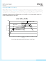
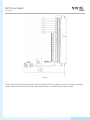
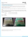
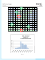
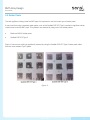
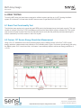
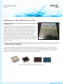
SMT Array Design
TECH NOTE
Building Arrays of SensL SMT Sensors on PCB
INTRODUCTION
This document focusses on the creation of close-packed arrays
of SiPM sensors. It describes the design and test of a 12x12 (144)
pixel array using 3mm surface mount (SMT) SiPM. Primarily, the
design was carried out to investigate the achievable pixel pitch and
planarity when producing arrays using these devices. To evaluate
the functionality of the array, it was decided to design the board
to have the necessary output to be compatible with the Matrix
readout system, which allowed for performance testing of the array.
Although the work here uses the MLP type of SMT sensor package,
all of the information applies equally to the creation of arrays using
SensL TSV parts.
1. SENSL SMT PACKAGES
This document contains information necessary for the user to create close-packed, 1D or 2D arrays of SensL
surface mount (SMT) compatible sensor packages; either the micro leadframe package (MLP) or through-silicon
via (TSV) parts. The MLP-SMT products have a part number with the suffix “-SMT“, whereas the TSV-SMT is
denoted by “-TSV“. Figure 1 below shows examples of each package type.
Figure 1, MLP-SMT parts (left) and TSV-SMT parts (right)
SensL © 2012
1
SMT Array Design
TECH NOTE
2. HANDLING OF MOISTURE SENSITIVE MLP-SMT AND TSV-SMT DEVICES
2.1 Applicable Documents
IPC/JEDEC J-STD-020; IPC/JEDEC J-STD-033.
2.2 Storage Conditions
SMT devices (both MLP and TSV) are moisture sensitive. Moisture can diffuse into the package from atmospheric
humidity. Surface mount soldering of the SMT packages to PCBs exposes the entire package body to
temperatures up to 260OC. Rapid expansion of trapped moisture during this process can result in package
cracking, delamination of critical interfaces within the package or damaged bond wires.
Parts are shipped in moisture barrier bags (MBBs). Unopened MBBs shall be stored at temperature below 40OC
with humidity below 90%RH. After the MBB has been opened, the devices must be reflow soldered within a
specific time period, as defined by the moisture sensitivity level (MSL). The MSL for SensL parts are shown in
Table 1. The parts must be baked according to J-STD-033, table 4.1 if any of the following occurs:
1. The parts are not reflow soldered within the given time period after opening the MBB.
2. The MBB is expired (according to the packing date and conditions on the label).
3. The humidity indicator card (HIC) shows the moisture level within the MBB has increased beyond the required
level.
Table 1, MSL values and details
SensL Package
MSL
Exposure time
Condition
TSV
2
1 year
≤30°C/60% RH
MLP
3
168 hours
≤30°C/60% RH
More detailed information about storing and handling the SMT parts can be found in the following Tech Note.
SensL © 2012
2
SMT Array Design
TECH NOTE
2.3 Solder Reflow Conditions
MLP and TSV products must be mounted according to specified soldering pad patterns. Refer to the product
User Manual for details (e.g. UM-MicroC.pdf). Solder paste (we recommend using no-clean solder paste) must be
evenly applied to each soldering pad to insure proper bonding and positioning of the component. After soldering,
allow at least three minutes for the component to cool to room temperature before further operations.
Solder reflow conditions must be in compliance with J-STD-20, table 5.2. This is summarized in Figure 2. The
number of passes shall not be more than 2.
Solder Reflow Profile
300
Max 260OC
Temperature (OC)
250
217OC
Max 4OC/sec
200
Max 10sec at 260OC
180OC
60~100sec
150
60 to 120 sec
100
50
0
0
50
100
150
200
250
300
Time (sec)
Figure 2, Solder reflow profile for the MLP-SMT and the TSV-SMT parts
SensL © 2012
3
SMT Array Design
TECH NOTE
3. ARRAY BUILD CONSIDERATIONS
The following key parameters should be taken into account when seeking a vendor to assemble the MLP or TSV
array, to ensure the best quality.
•Planarity
•
Minimum gap between sensor parts (fill factor)
•
Component placement accuracy
•
Board material
• Handling to the applicable MSL specifications (see page 2)
3.1 Planarity
The planarity is a measurement of how flat the board is. It is the deviation from 2 diagonal points as a percentage
of the diagonal measurement. For example, if two corners of a 30mm x 40mm board deviate by 0.4mm then the
planarity is:
0.4/50 = 0.8 (Diagonal of board is 50mm)
An example of good values for the key parameters are as follows:
Planarity
Minimum gap
Component placement
0.09% to 0.53%
0.2mm
+/-25um
SensL © 2012
4
SMT Array Design
TECH NOTE
4. TEST ARRAY ELECTRONICS DESIGN
A test array mounted on PCB was fabricated using SensL MLP packaged sensor parts. The array layout was
designed to be compatible with the SensL Matrix System, that could be used for evaluation.
Figure 3
Figure 3 shows one of 9 blocks designed to replicate the function of the 4x4 array used on the Matrix system
detector head, with each element representing an Micro-30035-SMT sensor. The 16 cathodes (N) of each 4x4
block of devices are connected together to create the 9 ARRAY signal lines. The corresponding anode (P) outputs
of each 4x4 block of devices are connected together to create 16 PIXEL signal lines. The positive bias is applied to
the ARRAY side of the device.
However, with alternative readout electronics, other routing of the signals is possible.
SensL © 2012
5
SMT Array Design
TECH NOTE
Figure 4
Figure 4 shows the ribbon cable connector and thermometer IC. This is identical to the circuit used for the Matrix
system detector head. Hence the board is electrically identical to the Matrix system detector head.
SensL © 2012
6
SMT Array Design
TECH NOTE
5. MANUFACTURING THE TEST ARRAY
Figure 5 shows the engineering drawing of the Micro-30035-SMT devices which was used for the test array. The
MLP package is nominally a 4mm x 4mm square housing the SiPM die of 3.16mm x 3.16mm. The information
below could also apply to an array based on the TSV parts, using CAD and pin-out information from the relevant
product User Manual.
The manufacturing challenge for this project was two-fold:
1.
MLP Device Spacing - manufacture a board with the devices as close as possible to ensure the best
possible fill factor.
2.
Planarity - manufacture the board with best planarity measurement as possible
Figure 5
Table 2 - Pad Numbering for the Micro-300XX
PAD
1
2
3
4
Connection
M-Series
B- or C-Series
Cathode
Anode
Fast Output
Fast Output
Anode
Cathode
Not Connected Not Connected
Common practice would be to ground any floating pins such as the NC pin (#4). Grounding the pin helps shielding
and keeps noise interference from external sources (EMI/RF) down but it may also be left floating without issue. In
the production of the PCBs discussed in this document, the NC pin was grounded.
In addition, it should be ensured that the assembly of the array board takes into account the MSL
specifications of the devices.
SensL © 2012
7
SMT Array Design
TECH NOTE
5.1 MLP Solder Footprint
The solder footprint shown in Figure 6 has been shown to work well for the 3mm MLP parts (e.g. Micro-30035SMT). It consists of four square 1.4mm x 1.4mm pads arranged in a square with a pitch of 1.8mm between pad
centres (0.4mm gap between pads). Solder footprint information for the TSV parts can be found in the relevant
product User Manual.
Figure 6
5.2 MLP Device Spacing
The MLP devices are cut from strips with a cut accuracy of +/-50um. Therefore, if the parts were placed with
100um spacing there could be extreme cases where the devices could touch. Therefore, to ensure that there
would always be a minimum spacing of 100um, a component spacing of 200um was chosen.
Figure 7 shows how this results in a variable gap between the devices ranging from 100um to 300um. Regardless
of this variation in outside package size, the position of the inner die will be fixed. Therefore based on a spacing of
200um the active areas will be 1.04mm apart. This gives an array fill factor of: (3.16)2 / (0.52 + 3.16)2 ~ 75%.
Note: The minimum spacing of 200um is too small to allow re-work. Should the user wish to design an array that
can be reworked, then a minimum of 500um spacing is recommended.
Figure 7
SensL © 2012
8
SMT Array Design
TECH NOTE
NOTE: The TSV parts are cut with greater accuracy and as a consequence can be placed with a minimum
spacing of 100um, although a minimum spacing of 500um is required if the user wishes to allow for rework.
5.3 Planarity
The vendor used for the array assembly believed that a simple 6 layer FR4 PCB would be acceptable providing
good care was taken during the manufacturing process.
The planarity of the resulting array is very much dependent on the process of soldering the devices to the board.
It was observed by the vendor that during the re-flow process it was important to hold the boards in a rigid frame
to avoid any warping due to the heat process. By designing a specific frame to hold the boards, less than 220um
warping diagonally from corner to corner was achieved with relative ease.
As the diagonal measurement of the board is 71mm (see Figure 8) this gives a planarity measurement of:
0.22 / 71 = 0.3%
This fits well inside the quoted range of 0.09% to 0.53%.
Figure 8
SensL © 2012
9
SMT Array Design
TECH NOTE
5.4 Detailed Planarity Measurements
Prototype boards were manufactured, as shown in Figure 9 (sensor side) and Figure 10 (rear connector side).
To fully test the planarity, one of the samples was analyzed using a non-contact optical instrument specifically
designed for this type of measurement.
The machine first takes the position of each corner of the board and from 2 diagonal lines it calculates the ideal
plane.
The position of the surface of each sensor pixel is then measured and compared with the ideal plane. An example
result from one of the prototype arrays is shown in Figure 11. It displays a value that tells you how close (+ or -) the
device is from the ideal plane for each pixel.
For example: Pixel 111 Pixel 80 is +0.005mm (5um above the ideal plane)
is -0.013mm (13um below the ideal plane)
Blue = +ve = ABOVE
Green = -ve = BELOW
Figure 9
Figure 10
The graph in Figure 12 shows the 144 values placed in 10um bins from -100 to +100um.
The results shows the range is -80 to +60 = 140um.
SensL © 2012
10
SMT Array Design
TECH NOTE
133
134
135
136
137
138
139
140
141
142
143
144
+0.031
+0.004
+0.001
+0.011
-0.012
-0.001
-0.019
-0.018
+0.014
-0.005
-0.019
+0.014
121
122
123
124
125
126
127
128
129
130
131
132
+0.028
+0.029
+0.003
+0.001
+0.007
-0.017
-0.022
+0.020
+0.003
-0.006
+0.019
+0.023
109
110
111
112
113
114
115
116
117
118
119
120
+0.027
+0.019
+0.005
+0.000
-0.009
-0.016
+0.045
-0.014
-0.003
-0.006
+0.024
+0.032
97
98
99
100
101
102
103
104
105
106
107
108
+0.030
+0.020
+0.001
-0.006
-0.009
+0.034
-0.017
-0.017
+0.007
+0.013
+0.036
+0.037
85
86
87
88
89
90
91
92
93
94
95
96
+0.030
+0.013
+0.001
-0.009
+0.052
-0.009
-0.009
-0.014
+0.015
+0.016
+0.034
+0.041
73
74
75
76
77
78
79
80
81
82
83
84
+0.033
+0.015
-0.002
+0.051
+0.003
-0.009
-0.016
-0.013
+0.014
+0.036
+0.031
+0.032
61
62
63
64
65
66
67
68
69
70
71
72
+0.021
+0.005
+0.040
-0.005
-0.012
-0.012
-0.013
-0.006
+0.026
+0.029
+0.005
+0.033
49
50
51
52
53
54
55
56
57
58
59
60
+0.009
+0.049
+0.008
-0.007
-0.013
-0.012
-0.015
-0.01
+0.013
+0.042
+0.026
+0.023
37
38
39
40
41
42
43
44
45
46
47
48
+0.029
-0.001
-0.011
-0.015
-0.026
-0.032
-0.025
-0.016
+0.002
+0.036
+0.021
+0.018
25
26
27
28
29
30
31
32
33
34
35
36
-0.013
-0.011
-0.029
-0.034
-0.041
-0.033
-0.039
-0.027
-0.001
+0.011
+0.028
+0.004
13
14
15
16
17
18
19
20
21
22
23
24
-0.035
-0.038
-0.047
-0.047
-0.058
-0.057
-0.052
-0.044
-0.011
+0.008
+0.023
+0.035
1
2
3
4
5
6
7
8
9
10
11
12
-0.017
-0.021
-0.013
-0.04
-0.072
-0.077
-0.076
-0.072
-0.059
-0.029
-0.006
+0.004
Figure 11
Figure 12
SensL © 2012
11
SMT Array Design
TECH NOTE
5.5 Solder Paste
To avoid significant voiding under the SMT pads it is important to use the correct type of solder paste.
It was found that using a standard solder paste, such as the Qualitek DSP 875 Type3, resulted in significant solder
voids formed under the SMT pads. This problem was resolved by using one of two solder pastes:
•
Multicore WS300 solder paste
•
Qualitek DSP 875 Type 5
Figure 13 shows how voiding is significantly reduced by using the Qualitek DSP 875 Type 5 solder paste rather
than the more standard Type 3 paste.
Figure 13
SensL © 2012
12
SMT Array Design
TECH NOTE
6. ARRAY TESTING
To test the MLP array, the board was connected to a Matrix system and then on to a PC hosting the Matrix
system GUI software. For these tests the MLP sensors were of type MicroFM-30035-SMT.
6.1 Basic Pixel Functionality Test
The initial test was carried out to prove that each SiPM pixel in the fabricated array functioned correctly. This was
carried out using a 3x3x15mm3 LYSO scintillating crystal and the SensL Matrix system software GUI. The crystal
was moved from pixel to pixel. Each time the GUI was used to verify that the particular pixel was detecting the
intrinsic radioactivity from the Lutetium in the LYSO crystal.
6.2 Cesium-137 Source Energy Resolution Measurement
Using a Cs-137 radioactive source (that produces gamma rays of 662keV) and a 3x3x15mm3 LYSO crystal,
energy resolution measurements were carried out on 9 different pixels. Figure 14 shows a typical energy plot using
the Matrix system GUI. It was found that, in all cases, it was relatively simple to achieve an energy resolution of
<12.5%.
Figure 14
All specifications are subject to change without notice
Rev. 2.1, March 2015
SensL
SensL©©2012
2012
www.sensl.com
[email protected]
+353 21 240 7110 (International)
+1 650 641 3278 (North America)
13