Download USER`S MANUAL ERRATA

Transcript
S3C84H5X/F84H5X_UM_REV 1.10
16
A/D CONVERTER
A/D CONVERTER
OVERVIEW
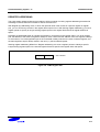
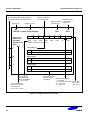
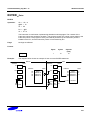
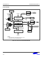
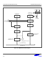
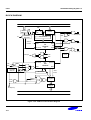
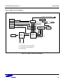
The 10-bit A/D converter (ADC) module uses successive approximation logic to convert analog levels entering at
one of the eight input channels to equivalent 10-bit digital values. The analog input level must lie between the
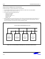
AVREF and AVSS values. The A/D converter has the following components:
•
Analog comparator with successive approximation logic
•
D/A converter logic (resistor string type)
•
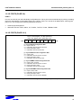
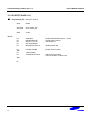
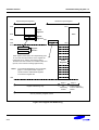
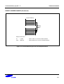
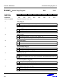
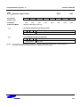
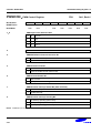
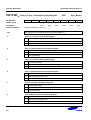
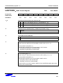
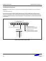
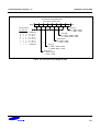
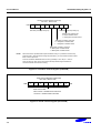
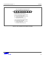
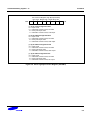
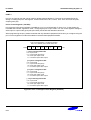
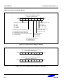
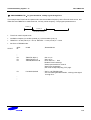
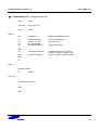
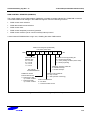
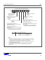
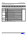
ADC control register, ADCON (set 1, bank 0, F7H, read/write, but ADCON.3 is read only)
•
Eight multiplexed analog data input pins (ADC0−ADC7)
•
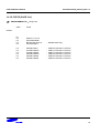
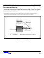
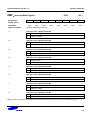
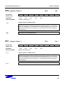
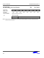
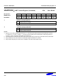
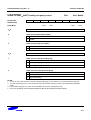
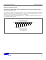
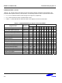
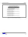
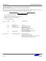
10-bit A/D conversion data output register (ADDATAH, ADDATAL)
FUNCTION DESCRIPTION
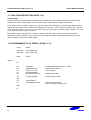
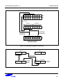
To initiate an analog-to-digital conversion procedure, at first, you must configure P0.0−P0.3, P2.2−P2.3,
P1.4−P1.5 to analog input before A/D conversions because the P0.0−P0.3, P2.2−P2.3, P1.4−P1.5 pins can be
used alternatively as normal data I/O or analog input pins. To do this, you load the appropriate value to the
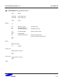
P0CONL, P2CONL and P1CONH (for ADC0−ADC7) register.
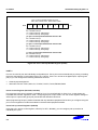
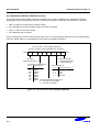
And you write the channel selection data in the A/D converter control register ADCON to select one of the eight
analog input pins (ADCn, n = 0−7) and set the conversion start or enable bit, ADCON.0. A 10-bit conversion
operation can be performed for only one analog input channel at a time. The read-write ADCON register is
located in set 1, bank 0 at address F7H.
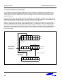
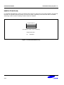
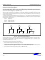
During a normal conversion, ADC logic initially sets the successive approximation register to 200H (the
approximate half-way point of an 10-bit register). This register is then updated automatically during each
conversion step. The successive approximation block performs 10-bit conversions for one input channel at a time.
You can dynamically select different channels by manipulating the channel selection bit value (ADCON.6−.4) in
the ADCON register.
To start the A/D conversion, you should set the enable bit, ADCON.0. When a conversion is completed,
ADCON.3, the end-of-conversion (EOC) bit is automatically set to 1 and the result is dumped into the ADDATAH,
ADDATAL registers where it can be read. The ADC module enters an idle state. Remember to read the contents
of ADDATAH and ADDATAL before another conversion starts. Otherwise, the previous result will be overwritten
by the next conversion result.
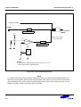
NOTE
Because the ADC does not use sample-and-hold circuitry, it is important that any fluctuations in the
analog level at the ADC0−ADC7 input pins during a conversion procedure be kept to an absolute
minimum. Any change in the input level, perhaps due to circuit noise, will invalidate the result.
16-1