1
USER'S MANUAL
S3F84Q5
8-BIT CMOS
MICROCONTROLLERS
Dec, 2007
REV 1.00
Confidential Proprietary of Samsung Electronics Co., Ltd
Copyright © 2007 Samsung Electronics, Inc. All Rights Reserved
Important Notice
The information in this publication has been carefully
checked and is believed to be entirely accurate at
the time of publication. Samsung assumes no
responsibility, however, for possible errors or
omissions, or for any consequences resulting from
the use of the information contained herein.
Samsung reserves the right to make changes in its
products or product specifications with the intent to
improve function or design at any time and without
notice and is not required to update this
documentation to reflect such changes.
This publication does not convey to a purchaser of
semiconductor devices described herein any license
under the patent rights of Samsung or others.
Samsung makes no warranty, representation, or
guarantee regarding the suitability of its products for
any particular purpose, nor does Samsung assume
any liability arising out of the application or use of
any product or circuit and specifically disclaims any
and all liability, including without limitation any
consequential or incidental damages.
"Typical" parameters can and do vary in different
applications. All operating parameters, including
"Typicals" must be validated for each customer
application by the customer's technical experts.
Samsung products are not designed, intended, or
authorized for use as components in systems
intended for surgical implant into the body, for other
applications intended to support or sustain life, or for
any other application in which the failure of the
Samsung product could create a situation where
personal injury or death may occur.
Should the Buyer purchase or use a Samsung
product for any such unintended or unauthorized
application, the Buyer shall indemnify and hold
Samsung and its officers, employees, subsidiaries,
affiliates, and distributors harmless against all
claims, costs, damages, expenses, and reasonable
attorney fees arising out of, either directly or
indirectly, any claim of personal injury or death that
may be associated with such unintended or
unauthorized use, even if such claim alleges that
Samsung was negligent regarding the design or
manufacture of said product.
S3F84Q5 8-Bit CMOS Microcontrollers
User's Manual, Revision 1.00
Publication Number: 02-1.00-S3-F84Q5-122007
Copyright © 2007 Samsung Electronics Co., Ltd.
All rights reserved. No part of this publication may be reproduced, stored in a retrieval system, or transmitted in
any form or by any means, electric or mechanical, by photocopying, recording, or otherwise, without the prior
written consent of Samsung Electronics.
Samsung Electronics' microcontroller business has been awarded full ISO-14001
certification (BSI Certificate No. FM24653). All semiconductor products are designed
and manufactured in accordance with the highest quality standards and objectives.
Samsung Electronics Co., Ltd.
San #24 Nongseo-Dong, Giheung-Gu
Yongin-City, Gyeonggi-Do, Korea
C.P.O. Box #37, 446-711
TEL: (82)-(31)-209-5238
FAX: (82)-(31)-209-6494
Home Page: http://www.samsung.com
Printed in the Republic of Korea
NOTIFICATION OF REVISIONS
ORIGINATOR:
Samsung Electronics, LSI Development Group, Gi-Heung, South Korea
PRODUCT NAME:
S3F84Q5 8-bit CMOS Microcontroller
DOCUMENT NAME:
S3F84Q5 User's Manual, Revision 1.00
DOCUMENT NUMBER:
21-S3-F84Q5-122007
EFFECTIVE DATE:
December, 2007
DIRECTIONS:
Revision 1.00
REVISION HISTORY
Revision No
Description of Change
Refer to
Author(s)
Date
0.00
Preliminary Spec for internal release only
−
−
Aug, 2006
1.00
First revision
−
HwiTaek. Chung
Dec, 2007
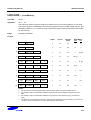
REVISION DESCRIPTIONS FOR REVISION 1.00
Chapter
Chapter Name
1. Overview
Page
1-2
Subjects (Major changes comparing with last version)
1) Changed operation voltage @1-10MHz from 4.0-5.5V to 3.0-5.5V
(also made the corresponding change in chapter 20: electrical Data)
2) Changed one of the LVR levels from 2.3V to 2.2V
(also made the corresponding change in chapter 20: electrical Data)
3) Added one more package 32-pin ELP
(also made the corresponding change in chapter 22:mechanical data)
2. Address
2-3
Changed LVR default status from enable to disable
5. Interrupt
5-17
Added one sentence: Please refer to IRET instruction in chapter 6
to clearly illustrate the proper usage of fast interrupt
19. Embedded Flash
Memory Interface
All Pages
The whole chapter was added in V1.0
20. LVR
All Pages
The whole chapter was added in V1.0
23. Tools
23-3
Redrew figure 23-2 and table 23-2 and table 23-3 to meet the current
version of S3F84Q5 target board.
Preface
The S3F84Q5 Microcontroller User's Manual is designed for application designers and programmers who are
using the S3F84Q5 microcontroller for application development. It is organized in two main parts:
Part I Programming Model
Part II Hardware Descriptions
Part I contains software-related information to familiarize you with the microcontroller's architecture, programming
model, instruction set, and interrupt structure. It has six chapters:
Chapter 1
Product Overview
Chapter 4
Control Registers
Chapter 2
Address Spaces
Chapter 5
Interrupt Structure
Chapter 3
Addressing Modes
Chapter 6
Instruction Set
Chapter 1, "Product Overview," is a high-level introduction to S3F84Q5 with general product descriptions, as well
as detailed information about individual pin characteristics and pin circuit types.
Chapter 2, "Address Spaces," describes program and data memory spaces, the internal register file, and register
addressing. Chapter 2 also describes working register addressing, as well as system stack and user-defined
stack operations.
Chapter 3, "Addressing Modes," contains detailed descriptions of the addressing modes that are supported by the
S3C8-series CPU.
Chapter 4, "Control Registers," contains overview tables for all mapped system and peripheral control register
values, as well as detailed one-page descriptions in a standardized format. You can use these easy-to-read,
alphabetically organized, register descriptions as a quick-reference source when writing programs.
Chapter 5, "Interrupt Structure," describes the S3F84Q5 interrupt structure in detail and further prepares you for
additional information presented in the individual hardware module descriptions in Part II.
Chapter 6, "Instruction Set," describes the features and conventions of the instruction set used for all S3C8-series
microcontrollers. Several summary tables are presented for orientation and reference. Detailed descriptions of
each instruction are presented in a standard format. Each instruction description includes one or more practical
examples of how to use the instruction when writing an application program.
A basic familiarity with the information in Part I will help you to understand the hardware module descriptions in
Part II. If you are not yet familiar with the S3C8-series microcontroller family and are reading this manual for the
first time, we recommend that you first read Chapters 1−3 carefully. Then, briefly look over the detailed
information in Chapters 4, 5, and 6. Later, you can reference the information in Part I as necessary.
Part II "hardware Descriptions," has detailed information about specific hardware components of the S3F84Q5
microcontroller. Also included in Part II are electrical, mechanical, OTP, and development tools data. It has 17
chapters:
Chapter 7
Clock Circuit
Chapter 16
14-bit PWM(pulse width modulation)
Chapter 8
RESET and Power-Down
Chapter 17
10-Bit Analog-To-Digital Converter
Chapter 9
I/O Ports
Chapter 18
Watch Timer
Chapter 10
Basic Timer
Chapter 19
Embedded Flash Memory Interface
Chapter 11
8-bit Timer A/B
Chapter 20
Low Voltage Reset
Chapter 12
16-bit Timer 1
Chapter 21
Electrical Data
Chapter 13
Timer 0
Chapter 22
Mechanical Data
Chapter 14
UART
Chapter 23
Development Tools
Chapter 15
Serial I/O Interface
S3F84Q5_UM_REV 1.00 MICROCONTROLLER
iii
Table of Contents
Part I — Programming Model
Chapter 1
Product Overview
S3C8-Series Microcontrollers ........................................................................................................................1-1
S3F84Q5 Microcontroller ...............................................................................................................................1-1
Features .........................................................................................................................................................1-2
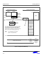
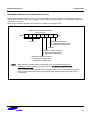
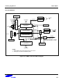
Block Diagram................................................................................................................................................1-3
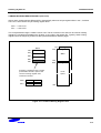
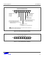
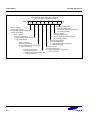
Pin Assignment ..............................................................................................................................................1-4
Pin Assignment ..............................................................................................................................................1-5
Pin Descriptions .............................................................................................................................................1-7
Pin Circuits .....................................................................................................................................................1-10
Chapter 2
Address Spaces
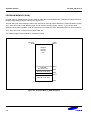
Overview ........................................................................................................................................................2-1
Program Memory (ROM) ...............................................................................................................................2-2
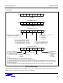
Register Architecture .....................................................................................................................................2-4
Register Page Pointer (PP) ..................................................................................................................2-6
Register Set 1 .......................................................................................................................................2-8
Register Set 2 .......................................................................................................................................2-8
Prime Register Space...........................................................................................................................2-9
Working Registers ................................................................................................................................2-10
Using the Register Pointers..................................................................................................................2-11
Register Addressing.......................................................................................................................................2-13
Common Working Register Area (C0H−CFH) .....................................................................................2-15
4-Bit Working Register Addressing ......................................................................................................2-16
8-Bit Working Register Addressing ......................................................................................................2-18
System and User Stack .................................................................................................................................2-20
Chapter 3
Addressing Modes
Overview ........................................................................................................................................................3-1
Register Addressing Mode (R).......................................................................................................................3-2
Indirect Register Addressing Mode (IR).........................................................................................................3-3
Indexed Addressing Mode (X) .......................................................................................................................3-7
Direct Address Mode (DA) .............................................................................................................................3-10
Indirect Address Mode (IA) ............................................................................................................................3-12
Relative Address Mode (RA) .........................................................................................................................3-13
Immediate Mode (IM) .....................................................................................................................................3-14
S3F84Q5_UM_REV 1.00 MICROCONTROLLER
v
Table of Contents (Continued)
Chapter 4
Control Registers
Overview........................................................................................................................................................ 4-1
Chapter 5
Interrupt Structure
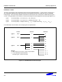
Overview........................................................................................................................................................ 5-1
Interrupt Types ..................................................................................................................................... 5-2
S3F84Q5 Interrupt Structure................................................................................................................ 5-3
System-Level Interrupt Control Registers............................................................................................ 5-6
Interrupt Processing Control Points ..................................................................................................... 5-7
Peripheral Interrupt Control Registers ................................................................................................. 5-8
System Mode Register (SYM) ............................................................................................................. 5-9
Interrupt Mask Register (IMR) ............................................................................................................. 5-10
Interrupt Priority Register (IPR)............................................................................................................ 5-11
Interrupt Request Register (IRQ)......................................................................................................... 5-13
Interrupt Pending Function Types........................................................................................................ 5-14
Interrupt Source Polling Sequence ...................................................................................................... 5-15
Interrupt Service Routines ................................................................................................................... 5-15
Generating interrupt Vector Addresses ............................................................................................... 5-16
Nesting of Vectored Interrupts ............................................................................................................. 5-16
Instruction Pointer (IP) ......................................................................................................................... 5-16
Fast Interrupt Processing..................................................................................................................... 5-16
Procedure for Initiating Fast Interrupts ................................................................................................ 5-17
Fast Interrupt Service Routine ............................................................................................................. 5-17
Relationship to Interrupt Pending Bit Types ........................................................................................ 5-17
Programming Guidelines ..................................................................................................................... 5-17
Chapter 6
Instruction Set
Overview........................................................................................................................................................ 6-1
Data Types........................................................................................................................................... 6-1
Register Addressing............................................................................................................................. 6-1
Addressing Modes ............................................................................................................................... 6-1
Flags Register (FLAGS)....................................................................................................................... 6-6
Flag Descriptions ................................................................................................................................. 6-7
Instruction Set Notation........................................................................................................................ 6-8
Condition Codes .................................................................................................................................. 6-12
Instruction Descriptions........................................................................................................................ 6-13
vi
S3F84Q5_UM_REV 1.00 MICROCONTROLLER
Table of Contents (Continued)
Part II Hardware Descriptions
Chapter 7
Clock Circuit
Overview ........................................................................................................................................................7-1
System Clock Circuit ............................................................................................................................7-1
Main Oscillator Circuits.........................................................................................................................7-2
Sub Oscillator Circuits ..........................................................................................................................7-2
Clock Status During Power-Down Modes ............................................................................................7-3
System Clock Control Register (CLKCON) ..........................................................................................7-4
Main/Subsystem Oscillator Selection (OSCCON)................................................................................7-5
Switching the CPU Clock......................................................................................................................7-6
Chapter 8
RESET and Power-Down
System Reset.................................................................................................................................................8-1
Overview...............................................................................................................................................8-1
Power-Down Modes.......................................................................................................................................8-4
Stop Mode ............................................................................................................................................8-4
Idle Mode ..............................................................................................................................................8-4
Hardware Reset Values........................................................................................................................8-5
Chapter 9
I/O Ports
Overview ........................................................................................................................................................9-1
Port Data Registers ..............................................................................................................................9-2
Port 0 ....................................................................................................................................................9-3
Port 1 ....................................................................................................................................................9-5
Port 2 ....................................................................................................................................................9-9
Port 3 ....................................................................................................................................................9-12
Chapter 10
Basic Timer
Overview ........................................................................................................................................................10-1
Basic Timer (BT) ............................................................................................................................................10-2
Basic Timer Control Register (BTCON) ...............................................................................................10-2
Basic Timer Function Description.........................................................................................................10-3
S3F84Q5_UM_REV 1.00 MICROCONTROLLER
vii
Table of Contents (Continued)
Chapter 11
8-Bit Timer A/B
8-Bit Timer A.................................................................................................................................................. 11-1
Overview .............................................................................................................................................. 11-1
Function Description ............................................................................................................................ 11-2
Timer A Control Register (TACON) ..................................................................................................... 11-3
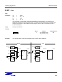
Block Diagram...................................................................................................................................... 11-5
8-Bit Timer B.................................................................................................................................................. 11-6
Overview .............................................................................................................................................. 11-6
Chapter 12
16-Bit Timer 1
Overview........................................................................................................................................................ 12-1
Function Description ............................................................................................................................ 12-2
Timer 1 Control Register (T1CON) ...................................................................................................... 12-3
Block Diagram...................................................................................................................................... 12-5
Chapter 13
Timer 0
One 16-Bit Timer Mode (Timer 0) ................................................................................................................. 13-1
Overview .............................................................................................................................................. 13-1
Function Description ............................................................................................................................ 13-1
Block Diagram ............................................................................................................................................... 13-3
Two 8-Bit Timers Mode (Timer C and D) ...................................................................................................... 13-4
Overview .............................................................................................................................................. 13-4
Function Description ............................................................................................................................ 13-7
Chapter 14
UART
Overview........................................................................................................................................................ 14-1
Programming Procedure...................................................................................................................... 14-1
UART Control Register (UARTCON)................................................................................................... 14-2
UART Interrupt Pending Register (UARTPND) ................................................................................... 14-3
Uart Data Register (UDATA)................................................................................................................ 14-4
Uart Baud Rate Data Register (BRDATA) ........................................................................................... 14-4
Baud Rate Calculations ....................................................................................................................... 14-5
Block Diagram ............................................................................................................................................... 14-6
Uart Mode 0 Function Description ....................................................................................................... 14-7
Uart Mode 1 Function Description ....................................................................................................... 14-8
Uart Mode 2 Function Description ....................................................................................................... 14-9
Serial Communication for Multiprocessor Configurations ................................................................... 14-11
viii
S3F84Q5_UM_REV 1.00
MICROCONTROLLER
Table of Contents (Continued)
Chapter 15
Serial I/O Interface
Overview ........................................................................................................................................................15-1
Programming Procedure ......................................................................................................................15-1
Serial I/O Control Registers (SIOCON) ................................................................................................15-2
SIO Prescaler Register (SIOPS) ..........................................................................................................15-3
Chapter 16
14-Bit PWM (Pulse Width Modulation)
Overview ........................................................................................................................................................16-1
Function Description ......................................................................................................................................16-1
PWM .....................................................................................................................................................16-1
PWM Control Register (PWMCON) .....................................................................................................16-5
Chapter 17
10-Bit Analog-To-Digital Converter
Overview ........................................................................................................................................................17-1
Function Description ......................................................................................................................................17-1
Conversion Timing................................................................................................................................17-2
A/D Converter Control Register (ADCON) ...........................................................................................17-2
Internal Reference Voltage Levels .......................................................................................................17-3
Block Diagram ...............................................................................................................................................17-4
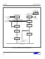
Internal A/D Conversion Procedure......................................................................................................17-5
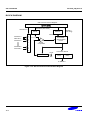
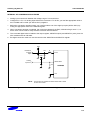
Chapter 18
Watch Timer
Overview ........................................................................................................................................................18-1
Watch Timer Control Register (WTCON) .............................................................................................18-2
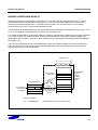
Watch Timer Circuit Diagram ...............................................................................................................18-3
S3F84Q5_UM_REV 1.00 MICROCONTROLLER
ix
Table of Contents (Continued)
Chapter 19
Embedded Flash Memory Interface
Overview........................................................................................................................................................ 19-1
User Program Mode ...................................................................................................................................... 19-2
Flash Memory Control Registers (User Program Mode) ..................................................................... 19-2
TM
ISP (On-Board Programming) Sector ....................................................................................................... 19-5
Sector Erase.................................................................................................................................................. 19-7
Programming ................................................................................................................................................. 19-9
Reading ......................................................................................................................................................... 19-10
Hard Lock Protection..................................................................................................................................... 19-11
Chapter 20
Low Voltage Reset
Overview ....................................................................................................................................................... 20-1
Chapter 21
Electrical Data
Overview ....................................................................................................................................................... 21-1
Chapter 22
Mechanical Data
Overview........................................................................................................................................................ 22-1
Chapter 23
Development Tools
Overview........................................................................................................................................................ 23-1
SHINE .................................................................................................................................................. 23-1
SASM ................................................................................................................................................... 23-1
SAMA Assembler ................................................................................................................................. 23-1
HEX2ROM ........................................................................................................................................... 23-1
Target Boards ...................................................................................................................................... 23-2
TB84Q5 Target Board.......................................................................................................................... 23-3
IDLE LED ............................................................................................................................................. 23-5
STOP LED ........................................................................................................................................... 23-5
OTP/MTP Programmer (Writer) ........................................................................................................... 23-9
x
S3F84Q5_UM_REV 1.00 MICROCONTROLLER
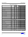
List of Figures
Figure
Number
Title
Page
Number
1-1
1-2
1-3
1-4
1-5
1-6
1-7
1-8
1-9
1-10
1-11
1-12
1-13
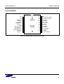
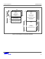
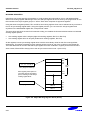
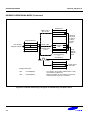
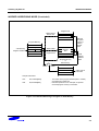
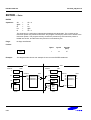
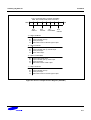
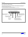
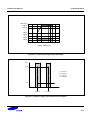
S3F84Q5 Block Diagram............................................................................................1-3
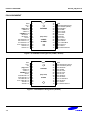
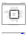
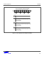
S3F84Q5 Pin Assignment (32-DIP, 32-SOP) ............................................................1-4
S3F84Q5 Pin Assignment (28-SOP)..........................................................................1-4
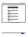
S3F84Q5 Pin Assignment (30-SDIP) .........................................................................1-5
S3F84Q5 Pin Assignment (32-ELP)...........................................................................1-6
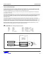
Pin Circuit Type 1 .......................................................................................................1-10
Pin Circuit Type 2 .......................................................................................................1-10
Pin Circuit Type 2-1 (P2.2, P2.4, P2.6, P3.0).............................................................1-10
Pin Circuit Type 1-1 (P0.0-0.1, P1.4-1.7, P2.0-2.1, P2.3, P2.5, P2.7, P3.1-3.2) .......1-10
Pin Circuit Type 1-2 (P1.0-1.1, P3.1-3.2) ...................................................................1-11
Pin Circuit Type 2-2 (P3.3-3.6, P3.0) .........................................................................1-11
Pin Circuit Type 2-3 (P0.2) .........................................................................................1-12
Pin Circuit Type 2-4 (P1.2-1.3) ...................................................................................1-12
2-1
2-2
2-3
2-4
2-5
2-6
2-7
2-8
2-9
2-10
2-11
2-12
2-13
2-14
2-15
2-16
Program Memory Address Space ..............................................................................2-2
Smart Option...............................................................................................................2-3
Internal Register File Organization (S3F84Q5)..........................................................2-5
Register Page Pointer (PP) ........................................................................................2-6
Set 1, Set 2, Prime Area Register Map ......................................................................2-9
8-Byte Working Register Areas (Slices) .....................................................................2-10
Contiguous 16-Byte Working Register Block .............................................................2-11
Non-Contiguous 16-Byte Working Register Block .....................................................2-12
16-Bit Register Pair ....................................................................................................2-13
Register File Addressing ............................................................................................2-14
Common Working Register Area................................................................................2-15
4-Bit Working Register Addressing ............................................................................2-17
4-Bit Working Register Addressing Example .............................................................2-17
8-Bit Working Register Addressing ............................................................................2-18
8-Bit Working Register Addressing Example .............................................................2-19
Stack Operations ........................................................................................................2-20
3-1
3-2
3-3
3-4
3-5
3-6
3-7
3-8
3-9
3-10
3-11
3-12
3-13
3-14
Register Addressing ...................................................................................................3-2
Working Register Addressing.....................................................................................3-2
Indirect Register Addressing to Register File.............................................................3-3
Indirect Register Addressing to Program Memory .....................................................3-4
Indirect Working Register Addressing to Register File ..............................................3-5
Indirect Working Register Addressing to Program or Data Memory ..........................3-6
Indexed Addressing to Register File ..........................................................................3-7
Indexed Addressing to Program or Data Memory with Short Offset ..........................3-8
Indexed Addressing to Program or Data Memory......................................................3-9
Direct Addressing for Load Instructions .....................................................................3-10
Direct Addressing for Call and Jump Instructions ......................................................3-11
Indirect Addressing.....................................................................................................3-12
Relative Addressing....................................................................................................3-13
Immediate Addressing................................................................................................3-14
S3F84Q5_UM_REV 1.00 MICROCONTROLLER
xi
List of Figures (Continued)
Figure
Number
Title
Page
Number
4-1
Register Description Format ...................................................................................... 4-4
5-1
5-2
5-3
5-4
5-5
5-6
5-7
5-8
5-9
S3C8/S3F8-Series Interrupt Types............................................................................ 5-2
S3F84Q5 Interrupt Structure ..................................................................................... 5-4
ROM Vector Address Area ........................................................................................ 5-5
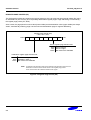
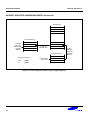
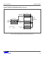
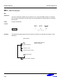
Interrupt Function Diagram ........................................................................................ 5-7
System Mode Register (SYM) ................................................................................... 5-9
Interrupt Mask Register (IMR) ................................................................................... 5-10
Interrupt Request Priority Groups .............................................................................. 5-11
Interrupt Priority Register (IPR) ................................................................................. 5-12
Interrupt Request Register (IRQ)............................................................................... 5-13
6-1
System Flags Register (FLAGS) ............................................................................... 6-6
7-1
7-2
7-3
7-4
7-5
7-6
7-7
7-8
Crystal/Ceramic Oscillator (fx) ................................................................................... 7-2
External Oscillator (fx)................................................................................................ 7-2
Crystal/Ceramic Oscillator (fxt) .................................................................................. 7-2
External Oscillator (fxt)............................................................................................... 7-2
System Clock Circuit Diagram ................................................................................... 7-3
System Clock Control Register (CLKCON) ............................................................... 7-4
Oscillator Control Register (OSCCON) ..................................................................... 7-5
STOP Control Register (STPCON)............................................................................ 7-7
8-1
8-2
8-3
Low Voltage Reset Circuit ......................................................................................... 8-2
Reset Block Diagram ................................................................................................. 8-3
Timing for S3F84Q5 after RESET ............................................................................. 8-3
9-1
9-2
9-3
9-4
9-5
9-6
9-7
9-8
9-9
9-10
Port 0 Control Register (P0CON) .............................................................................. 9-4
Port 1 High-Byte Control Register (P1CONH)........................................................... 9-6
Port 1 Low-Byte Control Register (P1CONL) ............................................................ 9-7
Port 1 Interrupt Control Register (P1INT) .................................................................. 9-8
Port 2 High-Byte Control Register (P2CONH)........................................................... 9-10
Port 2 Low-Byte Control Register (P2CONL) ............................................................ 9-11
Port 3 High-Byte Control Register (P3CONH)........................................................... 9-13
Port 3 Low-Byte Control Register (P3CONL) ............................................................ 9-14
Port 3 Interrupt Control Register (P3INT) .................................................................. 9-15
Port 3 Interrupt Pending Register (P3PND)............................................................... 9-15
10-1
10-2
10-3
Basic Timer Control Register (BTCON)..................................................................... 10-2
Oscillation Stabilization Time on RESET................................................................... 10-4
Oscillation Stabilization Time on STOP Mode Release............................................. 10-5
xii
S3F84Q5_UM_REV 1.00 MICROCONTROLLER
List of Figures (Concluded)
Figure
Number
Title
Page
Number
11-1
11-2
11-3
11-4
11-5
11-6
11-7
Timer A Control Register (TACON)............................................................................11-3
Timer Interrupts Pending Register (TINTPND) ..........................................................11-4
Timer A DATA Register (TADATA) ............................................................................11-4
Simplified Timer A Functional Block Diagram ............................................................11-5
Simplified Timer B Functional Block Diagram ............................................................11-6
Timer B Control Register (TBCON)............................................................................11-7
Timer B DATA Registers (TBDATA) ..........................................................................11-7
12-1
12-2
12-3
Timer 1 Control Register (T1CON).............................................................................12-3
Timer A/B/D and TIMER 1 Pending Register (TINTPND)..........................................12-4
Timer 1 Functional Block Diagram .............................................................................12-5
13-1
13-2
13-3
13-4
13-5
13-6
Timer 0 Control Register (TCCON) ............................................................................13-2
Timer 0 Functional Block Diagram .............................................................................13-3
Timer C Control Register (TCCON) ...........................................................................13-5
Timer D Control Register (TDCON) ...........................................................................13-6
Timer C and D Function Block Diagram.....................................................................13-8
Timer D PWM Function Block Diagram......................................................................13-9
14-1
14-2
14-3
14-4
14-5
14-6
14-7
14-8
14-9
14-10
UART Control Register (UARTCON) .........................................................................14-2
UART Interrupt Pending Register (UARTPND)..........................................................14-3
UART Data Register (UDATA) ...................................................................................14-4
UART Baud Rate Data Register (BRDATA) ..............................................................14-4
UART Functional Block Diagram................................................................................14-6
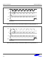
Timing Diagram for UART Mode 0 Operation ............................................................14-7
Timing Diagram for UART Mode 1 Operation ............................................................14-8
Timing Diagram for UART Mode 2 Operation ............................................................14-9
Timing Diagram for UART Mode 3 Operation ............................................................14-10
Connection Example for Multiprocessor Serial Data Communications .....................14-12
15-1
15-2
15-3
15-4
15-5
15-6
Serial I/O Interface Control Register (SIOCON).........................................................15-2
SIO Pre-Scaler Register (SIOPS) ..............................................................................15-3
SIO Functional Block Diagram ...................................................................................15-3
Serial I/O Timing in Transmit-Receive Mode (Tx at falling, SIOCON.4 = 0) ..............15-4
Serial I/O Timing in Transmit-Receive Mode (Tx at rising, SIOCON.4 = 1)...............15-4
Serial I/O Timing in Receive-Only Mode ....................................................................15-5
16-1
16-2
16-3
16-4
14-Bit PWM Basic Waveform .....................................................................................16-3
14-Bit Extended PWM Waveform...............................................................................16-4
PWM/Capture Module Control Register (PWMCON).................................................16-5
PWM Module Functional Block Diagram....................................................................16-6
S3F84Q5_UM_REV 1.00 MICROCONTROLLER
xiii
List of Figures (Concluded)
Figure
Number
Title
Page
Number
17-1
17-2
17-3
17-4
A/D Converter Control Register (ADCON) ................................................................ 17-2
A/D Converter Data Register (ADDATAH/L) ............................................................. 17-3
A/D Converter Functional Block Diagram.................................................................. 17-4
Recommended A/D Converter Circuit for Highest Absolute Accuracy...................... 17-5
18-1
18-2
Watch Timer Control Register (WTCON) .................................................................. 18-2
Watch Timer Circuit Diagram..................................................................................... 18-3
19-1
19-2
19-3
19-4
19-5
19-6
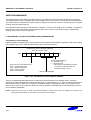
Flash Memory Control Register (FMCON) ................................................................ 19-2
Flash Memory User Programming Enable Register (FMUSR).................................. 19-3
Flash Memory Sector Address Register, High Byte (FMSECH) ............................... 19-4
Flash Memory Sector Address Register, Low Byte (FMSECL)................................. 19-4
Program Memory Address Space.............................................................................. 19-5
Sector Configurations in User Program Mode........................................................... 19-7
20-1
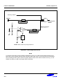
Low Voltage Reset Circuit ......................................................................................... 20-2
21-1
21-2
21-3
21-4
21-5
Input Timing Measurement Points ............................................................................. 21-4
Operating Voltage Range (S3F84Q5) ....................................................................... 21-5
Schmitt Trigger Input Characteristic Diagram............................................................ 21-5
Stop Mode Release Timing When Initiated by a RESET .......................................... 21-7
Definition of DLE and ILE........................................................................................... 21-9
22-1
22-2
22-3
22-4
22-5
32-SOP-450A Package Dimensions ......................................................................... 22-1
32-SDIP-400 Package Dimensions ........................................................................... 22-2
28-SOP-375 Package Dimensions ............................................................................ 22-3
30-Pin SDIP Package Dimensions ............................................................................ 22-4
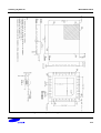
32-Pin ELP Package Dimensions.............................................................................. 22-5
23-1
23-2
23-3
23-4
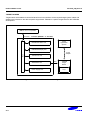
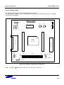
SMDS+ or SK-1000 Product Configuration ............................................................... 23-2
S3F84Q5 Target Board Configuration ....................................................................... 23-3
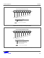
40-Pin Connector Pin Assignment for TB84Q5 ......................................................... 23-6
TB84Q5 Adapter Cable.............................................................................................. 23-7
xiv
S3F84Q5_UM_REV 1.00
MICROCONTROLLER
List of Tables
Table
Number
Title
Page
Number
1-1
1-2
1-3
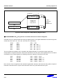
Pin Descriptions of 28-SOP (32-SOP, 32-SDIP / 30-SDIP) .......................................1-7
Pin Descriptions of 28-SOP (32-SOP,32-SDIP / 30-SDIP) ........................................1-8
Descriptions of Pins Used to Read/Write the Flash ROM..........................................1-9
2-1
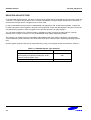
S3F84Q5 Register Type Summary ............................................................................2-4
4-1
4-2
4-3
Set 1 Registers ...........................................................................................................4-1
Set 1, Bank 0 Registers..............................................................................................4-2
Set 1, Bank 1 Registers..............................................................................................4-3
5-1
5-2
Interrupt Control Register Overview ...........................................................................5-6
Interrupt Source Control and Data Registers .............................................................5-8
6-1
6-2
6-3
6-4
6-5
6-6
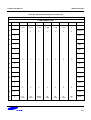
Instruction Group Summary........................................................................................6-2
Flag Notation Conventions .........................................................................................6-8
Instruction Set Symbols..............................................................................................6-8
Instruction Notation Conventions ...............................................................................6-9
Opcode Quick Reference ...........................................................................................6-10
Condition Codes .........................................................................................................6-12
8-1
8-2
8-3
S3F84Q5 Set1 Registers Values after RESET ..........................................................8-5
S3F84Q5 Set1 Bank0 Registers Values after RESET...............................................8-6
S3F84Q5 Set1 Bank1 Registers Values after RESET...............................................8-7
9-1
9-2
S3F84Q5 Port Configuration Overview ......................................................................9-1
Port Data Register Summary......................................................................................9-2
13-1
13-2
PWM Control and Data Registers ..............................................................................13-2
PWM output "stretch" Values for Extension Data Register (PWMDATAL .1–.0) .......13-3
14-1
Commonly Used Baud Rates Generated by 8-bit BRDATA ......................................14-5
16-1
16-2
PWM Control and Data Registers ..............................................................................16-2
PWM output "stretch" Values for Extension Registers...............................................16-3
19-1
19-2
ISP Sector Size...........................................................................................................19-6
Reset Vector Address.................................................................................................19-6
S3F84Q5_UM_REV 1.00 MICROCONTROLLER
xv
List of Tables
Table
Number
Title
Page
Number
21-1
21-2
21-3
21-4
21-5
21-6
21-7
21-8
21-9
Absolute Maximum Ratings ....................................................................................... 21-2
D.C. Electrical Characteristics ................................................................................... 21-3
A.C. Electrical Characteristics ................................................................................... 21-4
Oscillator Characteristics ........................................................................................... 21-6
Oscillation Stabilization Time..................................................................................... 21-6
Data Retention Supply Voltage in Stop Mode ........................................................... 21-7
LVR(Low Voltage Reset) Circuit Characteristics .................................................... 21-7
A/D Converter Electrical Characteristics ................................................................... 21-8
AC Electrical Characteristics for Internal Flash ROM (S3F84Q5 only) ..................... 21-9
23-1
23-2
23-3
23-4
Power Selection Settings for TB84Q5 ....................................................................... 23-4
DIP Switch for Smart Option Configuration ............................................................... 23-4
DIP Switch for Sub Oscillator Alternative Pins .......................................................... 23-4
Using Single Header Pins as the Input Path for External Trigger Sources ............... 23-5
xvi
S3F84Q5_UM_REV 1.00 MICROCONTROLLER
List of Programming Tips
Description
Chapter 2:
Page
Number
Address Spaces
Using the Page Pointer for RAM Clear (Page 0, Page 1)..............................................................................2-7
Setting the Register Pointers .........................................................................................................................2-11
Using the RPs to Calculate the Sum of a Series of Registers.......................................................................2-12
Addressing the Common Working Register Area..........................................................................................2-16
Standard Stack Operations Using PUSH and POP.......................................................................................2-21
Chapter 7:
Clock Circuit
Switching the CPU clock................................................................................................................................7-6
Chapter 10:
Basic Timer
Configuring the Basic Timer...........................................................................................................................10-6
Chapter 12:
16-bit Timer 1
Using the Timer 1...........................................................................................................................................12-6
Chapter 15:
Serial I/O Interface
SIO .................................................................................................................................................................15-5
Chapter 16:
14-Bit PWM (Pulse Width Modulation)
Programming the PWM Module to Sample Specifications ............................................................................16-7
Chapter 19:
Embedded Flash Memory Interface
Sector Erase ..................................................................................................................................................19-8
Program .........................................................................................................................................................19-9
Reading ..........................................................................................................................................................19-10
Hard Lock Protection .....................................................................................................................................19-11
S3F84Q5_UM_REV 1.00 MICROCONTROLLER
xvii
List of Register Descriptions
Register
Identifier
FLAGS
FMCON
FMSECH
FMSECL
FMUSR
IPH
IPL
IRQ
OSCCON
P0CON
P1CONH
P1CONL
P1INT
P2CONH
P2CONL
P3CONH
P3CONL
P3INT
P3PND
P3PND
PP
PWMCON
RP0
RP1
SIOCON
SIOPS
SPH
STPCON
SYM
T1CON
TBCON
TCCON
TDCON
TINTPND
UARTCON
UARTPND
WTCON
Full Register Name
Page
Number
System Flags Register ............................................................................................... 4-8
Flash Memory Control Register ................................................................................. 4-9
Flash Memory Sector Address Register (High Byte) ................................................. 4-10
Flash Memory Sector Address Register (Low Byte) .................................................. 4-10
Flash Memory User Programming Enable Register .................................................. 4-11
Instruction Pointer (High Byte) ................................................................................... 4-13
Instruction Pointer (Low Byte) .................................................................................... 4-13
Interrupt Request Register ......................................................................................... 4-15
Oscillator Control Register ......................................................................................... 4-16
Port 0 Control Register............................................................................................... 4-17
Port 1 Control Register (High Byte)............................................................................ 4-18
Port 1 Control Register (Low Byte) ............................................................................ 4-19
Port 1 Interrupt Control Register ................................................................................ 4-20
Port 2 Control Register (High Byte)............................................................................ 4-21
Port 2 Control Register (Low Byte) ............................................................................ 4-22
Port 3 Control Register (High Byte)............................................................................ 4-23
Port 3 Control Register (Low Byte) ............................................................................ 4-24
Port 3 Interrupt Enable Register................................................................................. 4-25
Port 3 Interrupt Pending Register............................................................................... 4-26
Port 3 Interrupt Pending Register............................................................................... 4-27
Register Page Pointer ................................................................................................ 4-28
PWM Control Register................................................................................................ 4-29
Register Pointer 0....................................................................................................... 4-30
Register Pointer 1....................................................................................................... 4-30
Serial I/O Module Control Registers........................................................................... 4-31
SIO Prescaler Register .............................................................................................. 4-32
Stack Pointer (High Byte) ........................................................................................... 4-32
Stop Control Register ................................................................................................. 4-33
System Mode Register ............................................................................................... 4-34
Timer 1 Control Register ............................................................................................ 4-35
Timer B Control Register............................................................................................ 4-37
Timer C Control Register ........................................................................................... 4-38
Timer D Control Register ........................................................................................... 4-39
Interrupt Pending Register ......................................................................................... 4-40
UART Control Register .............................................................................................. 4-41
UART Pending and Parity Control ............................................................................. 4-42
Watch Timer Control Register.................................................................................... 4-43
S3F84Q5_UM_REV 1.00 MICROCONTROLLER
xix
List of Instruction Descriptions
Instruction
Mnemonic
ADC
ADD
AND
BAND
BCP
BITC
BITR
BITR
BITS
BOR
BTJRF
BTJRT
BXOR
CALL
CCF
CLR
COM
CP
CPIJE
CPIJNE
DA
DA
DEC
DECW
DI
DIV
DJNZ
EI
ENTER
EXIT
IDLE
INC
INCW
IRET
JP
JR
LD
LD
LDB
Full Register Name
Page
Number
Add with Carry............................................................................................................ 6-14
Add ............................................................................................................................. 6-15
Logical AND ............................................................................................................... 6-16
Bit AND....................................................................................................................... 6-17
Bit Compare ............................................................................................................... 6-18
Bit Complement.......................................................................................................... 6-19
Bit Reset ..................................................................................................................... 6-20
Bit Reset ..................................................................................................................... 6-20
Bit Set ......................................................................................................................... 6-21
Bit OR ......................................................................................................................... 6-22
Bit Test, Jump Relative on False ............................................................................... 6-23
Bit Test, Jump Relative on True................................................................................. 6-24
Bit XOR....................................................................................................................... 6-25
Call Procedure............................................................................................................ 6-26
Complement Carry Flag ............................................................................................. 6-27
Clear ........................................................................................................................... 6-28
Complement ............................................................................................................... 6-29
Compare..................................................................................................................... 6-30
Compare, Increment, and Jump on Equal ................................................................. 6-31
Compare, Increment, and Jump on Non-Equal ......................................................... 6-32
Decimal Adjust ........................................................................................................... 6-33
Decimal Adjust ........................................................................................................... 6-34
Decrement.................................................................................................................. 6-35
Decrement Word ........................................................................................................ 6-36
Disable Interrupts ....................................................................................................... 6-37
Divide (Unsigned)....................................................................................................... 6-38
Decrement and Jump if Non-Zero.............................................................................. 6-39
Enable Interrupts ........................................................................................................ 6-40
Enter ........................................................................................................................... 6-41
Exit.............................................................................................................................. 6-42
Idle Operation............................................................................................................. 6-43
Increment ................................................................................................................... 6-44
Increment Word.......................................................................................................... 6-45
Interrupt Return .......................................................................................................... 6-46
Jump........................................................................................................................... 6-47
Jump Relative............................................................................................................. 6-48
Load............................................................................................................................ 6-49
Load............................................................................................................................ 6-50
Load Bit ...................................................................................................................... 6-51
S3F84Q5_UM_REV 1.00 MICROCONTROLLER
xxi
List of Instruction Descriptions (Continued)
Instruction
Mnemonic
LDC/LDE
LDC/LDE
LDCD/LDED
LDCI/LDEI
`LDCPD/LDEPD
LDCPD/LDEPD
LDCPI/LDEPI
LDW
MULT
NEXT
NOP
OR
POP
POPUD
POPUI
PUSH
PUSHUD
PUSHUI
RCF
RET
RL
RLC
RR
RRC
SB0
SB1
SBC
SCF
SRA
SRP/SRP0/SRP1
STOP
SUB
SWAP
TCM
TM
WFI
XOR
xxii
Full Register Name
Page
Number
Load Memory..............................................................................................................6-52
Load Memory..............................................................................................................6-53
Load Memory and Decrement ....................................................................................6-54
Load Memory and Increment......................................................................................6-55
Load Memory with Pre-Decrement.............................................................................6-55
Load Memory with Pre-Decrement.............................................................................6-56
Load Memory with Pre-Increment ..............................................................................6-57
Load Word ..................................................................................................................6-58
Multiply (Unsigned) .....................................................................................................6-59
Next.............................................................................................................................6-60
No Operation ..............................................................................................................6-61
Logical OR ..................................................................................................................6-62
Pop from Stack ...........................................................................................................6-63
Pop User Stack (Decrementing).................................................................................6-64
Pop User Stack (Incrementing) ..................................................................................6-65
Push to Stack..............................................................................................................6-66
Push User Stack (Decrementing)...............................................................................6-67
Push User Stack (Incrementing) ................................................................................6-68
Reset Carry Flag.........................................................................................................6-69
Return .........................................................................................................................6-70
Rotate Left ..................................................................................................................6-71
Rotate Left through Carry ...........................................................................................6-72
Rotate Right................................................................................................................6-73
Rotate Right through Carry.........................................................................................6-74
Select Bank 0..............................................................................................................6-75
Select Bank 1..............................................................................................................6-76
Subtract with Carry .....................................................................................................6-77
Set Carry Flag.............................................................................................................6-78
Shift Right Arithmetic ..................................................................................................6-79
Set Register Pointer....................................................................................................6-80
Stop Operation............................................................................................................6-81
Subtract ......................................................................................................................6-82
Swap Nibbles..............................................................................................................6-83
Test Complement under Mask ...................................................................................6-84
Test under Mask .........................................................................................................6-85
Wate for Interrupt........................................................................................................6-86
Logical Exclusive OR..................................................................................................6-87
S3F84Q5_UM_REV 1.00 MICROCONTROLLER
SF84Q5_UM_REV1.00
1
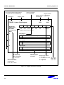
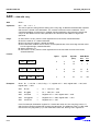
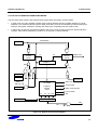
PRODUCT OVERVIEW
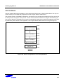
PRODUCT OVERVIEW
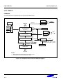
S3C8-SERIES MICROCONTROLLERS
Samsung's SAM8RC family of 8-bit single-chip CMOS microcontrollers offer a fast and efficient CPU, a wide
range of integrated peripherals, and various mask-programmable ROM sizes.
An address/data bus architecture and a large number of bit-configurable I/O ports provide a flexible programming
environment for applications with varied memory and I/O requirements. Timer/counters with selectable operating
modes are included to support real-time operations.
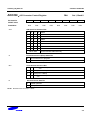
S3F84Q5 MICROCONTROLLER
The S3F84Q5 single-chip CMOS microcontrollers are fabricated using the highly advanced CMOS process
technology based on Samsung’s latest CPU architecture.
The S3F84Q5 is a microcontroller with a 16K-byte full-flash ROM embedded.
Using a proven modular design approach, Samsung engineers have successfully developed the S3F84Q5 by
integrating the following peripheral modules with the powerful SAM8 RC core:
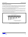
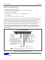
•
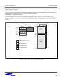
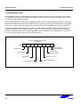
Four configurable I/O ports (22 pins / 24pins / 26pin)
•
Twenty-three interrupt sources with twenty-three vectors and eight interrupt level
•
One watchdog timer function (Basic Timer)
•
One 8-bit basic timer for oscillation stabilization
•
Four 8-bit timer/counters with time interval, PWM, and Capture mode
(Timer C and Timer D can be used for 16-bit Timer 0)
•
One 16-bit timer/counter with three operating modes; Interval timer, Capture and PWM mode
(If Timer C and Timer D are used for Timer 0, S3F84Q5 has two 16-bit Timer; Timer 0 and Timer 1)
•
Analog to digital converter with 8 input channels and 10-bit resolution
•
One asynchronous UART and one synchronous SIO
•
One Watch timer for real time operation
•
High current LED drive I/O ports (High current output: typical 12 mA)
The S3F84Q5 microcontroller is ideal for use in a wide range of home applications requiring simple timer/counter,
ADC, etc. They are currently available in 32-pin SOP/SDIP, 28-pin SOP, 30-pin SDIP and 32-ELP-0505 package.
NOTE
The S3F84Q5 is perfectly “pin-to-pin” compatible with the SAM88RCRI product S3C9498/F9498.
1-1
PRODUCT OVERVIEW
SF84Q5_UM_REV1.00
FEATURES
CPU
•
SAM8RC CPU core
Memory
•
•
528-byte general purpose register (RAM)
16K-byte internal multi time program memory
Full-Flash
√ Sector size: 128 Bytes
√ 10 Years data retention
√ Fast programming time:
+ Chip erase: 10ms
+ Sector erase: 10ms
+ Byte program: 30us
√ User programmable by ‘LDC’ instruction
√ Endurance: 10,000 erase/program cycles
√ Sector(128-bytes) erase available
√ Byte programmable
√ External serial programming support
√ Expandable OBPTM(On board program)
sector
Oscillation Sources
•
•
•
Crystal, or ceramic for main clock (10MHz max)
Crystal for sub clock (32.768kHz)
CPU clock divider (1/1, 1/2, 1/8, 1/16)
Instruction Set
•
•
78 instructions
IDLE and STOP instructions added for powerdown modes
Instruction Execution Time
•
400 ns at 10-MHz fxx (minimum, main clock)
•
122 µs at 32.768kHz (minimum, sub clock)
Interrupts
•
23 interrupt sources (9 external and 14 internal)
with 23 vectors / 8 levels
I/O Ports
•
•
•
Timer 0 Timer/Counters
•
•
•
•
1-2
One 8-bit timer/counter (Timer A) with three
operating modes; Interval mode, capture mode
and PWM mode
Real-time and interval time measurement
•
Four frequency output (0.5/1/2/4kHz) to BUZ pin
PWM module
•
•
14-bit PWM
8-bit base + 6-bit extension frame
A/D Converter
•
•
Eight analog input channels
10-bit conversion resolution
Serial I/O
•
•
One synchronous serial I/O module
Selectable transmit and receive rates.
Asynchronous UART
•
•
Programmable baud rate generator
Support serial data transmit/receive operations
with 8-bit, 9-bit UART
Low Voltage Reset (LVR)
•
•
Low Voltage Check to make system reset
VLVR = 2.2V, 3.0V, 4.0V (by smart option)
Operating Temperature Range
•
−40 °C to + 85 °C
Operating Voltage Range
•
Total 22/24/26 bit-programmable pins
One programmable 8-bit basic timer (BT) for
Oscillation stabilization control
Timers
The programmable 8-bit timer/counters
Configurable as one 16-bit timer/counter
Watch Timer
Basic Timer
•
One 8-bit timer/counter (Timer B) with 2
operating modes: interval mode and PWM mode
One 16-bit capture timer/counter (Timer 1) with
three operating modes; Interval mode, Capture
mode for pulse period or duty and PWM mode.
2.0 V to 5.5 V @ 1 ~ 4MHz (LVR Disable)
LVR to 5.5 V @ 1 ~ 4MHz (LVR Enable)
3.0 V to 5.5 V @ 1 ~ 10MHz
Package Type
•
28-pin SOP, 30-pin SDIP, 32-pin SDIP/SOP,
32-pin ELP
SF84Q5_UM_REV1.00
PRODUCT OVERVIEW
BLOCK DIAGRAM
PWM
(ADC0-7)
PWM
A/D
XIN
XOUT,XTOUT
nRESET
P0.0P0.2
Port 1
P1.0P1.7
Port 2
P2.0P2.7
Port 3
P3.0P3.6
SIO
SI
SO
SCK
UART
TXD
RXD
OSC/nRESET
8-Bit
Basic Timer
TAOUT
TACK
TACAP
8-Bit
Timer
/Counter A
T1OUT
T1CK
T1CAP
16-bit
Timer
/Counter 1
TBOUT
8-Bit
Timer
/Counter B
TDOUT
Port 0
I/O Port and Interrupt Control
SAM8RC CPU
8/16-Kbyte
ROM
272/528-Byte
RAM
8-Bit timer
C/D
Watch Timer
BUZ
Figure 1-1. S3F84Q5 Block Diagram
1-3
PRODUCT OVERVIEW
SF84Q5_UM_REV1.00
PIN ASSIGNMENT
VSS
XOUT
XIN
(Vpp)TEST
RxD/P0.0
TxD/P0.1
nRESET/P0.2
INT5/P3.3
INT6/P3.4
AVREF
INT0/ADC0/P1.0
INT1/ADC1/P1.1
XTIN/ADC2/P1.2
XTOUT/ADC3/P1.3
ADC4/P1.4
ADC5/P1.5
1
2
3
4
5
6
7
8
9
10
11
12
13
14
15
16
S3F84Q5
(Top View)
32-SOP
32-SDIP
32
31
30
29
28
27
26
25
24
23
22
21
20
19
18
17
VDD
P3.2/SCK/INT4(SCLK)
P3.1/SO/INT3(SDAT)
P3.0/SI/INT2
P2.7/PWM
P2.6/T1CAP
P2.5/T1OUT
P3.6/INT8
P3.5/INT7
P2.4/T1CK
P2.3/TBOUT
P2.2/TACAP
P2.1/TACK/BUZ
P2.0/TAOUT
P1.7/ADC7
P1.6/ADC6/TDOUT
Figure 1-2. S3F84Q5 Pin Assignment (32-DIP, 32-SOP)
VSS
XOUT
XIN
(Vpp)TEST
RxD/P0.0
TxD/P0.1
nRESET/P0.2
AVREF
INT0/ADC0/P1.0
INT1/ADC1/P1.1
XTIN/ADC2/P1.2
XTOUT/ADC3/P1.3
ADC4/P1.4
ADC5/P1.5
1
2
3
4
5
6
7
8
9
10
11
12
13
14
S3F84Q5
(Top View)
28-SOP
28
27
26
25
24
23
22
21
20
19
18
17
16
15
VDD
P3.2/SCK/INT4 (SCLK)
P3.1/SO/INT3 (SDAT)
P3.0/SI/INT2
P2.7/PWM
P2.6/T1CAP
P2.5/T1OUT
P2.4/T1CK
P2.3/TBOUT
P2.2/TACAP
P2.1/TACK/BUZ
P2.0/TAOUT
P1.7/ADC7
P1.6/ADC6/TDOUT
Figure 1-3. S3F84Q5 Pin Assignment (28-SOP)
1-4
SF84Q5_UM_REV1.00
PRODUCT OVERVIEW
PIN ASSIGNMENT
VSS
XOUT
XIN
(Vpp)TEST
RxD/P0.0
TxD/P0.1
nRESET/P0.2
INT5/P3.3
AVREF
INT0/ADC0/P1.0
INT1/ADC1/P1.1
XTIN/ADC2/P1.2
XTOUT/ADC3/P1.3
ADC4/P1.4
ADC5/P1.5
1
2
3
4
5
6
7
8
9
10
11
12
13
14
15
S3F84Q5
(Top View)
30-SDIP
30
29
28
27
26
25
24
23
22
21
20
19
18
17
16
VDD
P3.2/SCK/INT4 (SCLK)
P3.1/SO/INT3 (SDAT)
P3.0/SI/INT2
P2.7/PWM
P2.6/T1CAP
P2.5/T1OUT
P3.5/INT7
P2.4/T1CK
P2.3/TBOUT
P2.2/TACAP
P2.1/TACK/BUZ
P2.0/TAOUT
P1.7/ADC7
P1.6/ADC6/TDOUT
Figure 1-4. S3F84Q5 Pin Assignment (30-SDIP)
1-5
P3.5/INT7
P2.4/T1CK
P2.3/TBOUT
20
19
18
P2.2/TACAP
P3.6/INT8
21
17
P2.5/T1OUT
22
25
P2.6/T1CAP
24
INT2/SI/P3.0
23
SF84Q5_UM_REV1.00
P2.7/PWM
PRODUCT OVERVIEW
16
P2.1/TACK/BUZ
12
P1.5/ADC5
Xout
30
(32-ELP)
11
P1.4/ADC4
Xin
31
10
P1.3/ADC3/XTOUT
(Vpp)TEST
32
9
INT1/ADC1/P1.1
Top View
8
29
7
VSS
INT0/ADC0/P1.0
P1.6/ADC6/TDOUT
6
13
AVREF
S3F84Q5
5
28
INT6/P3.4
VDD
4
P1.7/ADC7
INT5/P3.3
14
3
27
nRESET/P0.2
(SCLK)INT4/SCK/P3.2
2
P2.0/TAOUT
TxD/P0.1
15
1
26
RxD/P0.0
(SDAT)INT3/SO/P3.1
Figure 1-5. S3F84Q5 Pin Assignment (32-ELP)
1-6
P1.2/ADC2/XTIN
SF84Q5_UM_REV1.00
PRODUCT OVERVIEW
PIN DESCRIPTIONS
Table 1-1. Pin Descriptions of 28-SOP (32-SOP, 32-SDIP / 30-SDIP)
Pin
Names
P0.0, P0.1
Pin
Type
Pin Description
Circuit
Type
Pin
No.
Shared
Functions
I/O
I/O port with bit-programmable pins.
Configurable to input or push-pull output
mode. P0.2 can be configured to open
drain output mode. Pull-up resistors can
be assigned by software. Pins can also
be assigned individually as alternative
function pins.
1-1
5-7
RxD, TxD
I/O port with bit-programmable pins.
Configurable to input or push-pull output
mode. Pull-up resistors can be assigned
by software. Pins can also be assigned
individually as alternative function pins.
1-2
I/O port with bit-programmable pins.
Configurable to input mode, push-pull
output mode. pin2.6,2.4,2.2 can be
configured to n-channel open-drain
output mode. Input mode with pull-up
resistors can be assigned by software.
Pins can also be assigned individually as
alternative function pins.
1-1
P0.2
P1.0, P1.1
P1.4-P1.7
I/O
P1.2, P1.3
P2.0,P2.1,P2.3
I/O
P2.5,P2.7
P2.2,P2.4,P2.6
P3.0
I/O
P3.1,P3.2
(P3.3-P3.6)
XOUT, XIN
I/O
I/O port with bit-programmable pins.
Configurable to input or push-pull output
mode. P3.0,P3.3-3.6 can be configured
to open drain output mode. Pull-up
resistors can be assigned by software.
Pins can also be assigned individually as
alternative function pins.
2-3
RESETB
9-16
( 11-18 /
11-18 )
XTIN, XTOUT
2-4
2-1
2-2
1-2
2-2
INT0-INT1
ADC0-ADC7
TDOUT
17-24
( 19-23,
26-28 /
19-23,
24-26)
TAOUT/TACK
TACAP
TBOUT
T1CAP/T1CK/BUZ
T1OUT
PWM
25-27
( 29-31,
8-9,
24-25
/ 27-29,
8, 23 )
SI/SO/SCK/INT2INT4 (INT5-INT8)
System clock input and output pins
−
2,3
−
TEST
I
Test signal input pin (for factory use only;
must be connected to VSS in normal
mode). Pull-down register is connected
internally.
−
4
_
VDD
−
Power supply input pin
−
28 (32/30)
−
VSS
−
Ground pin
−
1
−
1-7
PRODUCT OVERVIEW
SF84Q5_UM_REV1.00
Table 1-2. Pin Descriptions of 28-SOP (32-SOP,32-SDIP / 30-SDIP)
Pin
Names
Pin
Type
Pin Description
Circuit
Type
Pin
No.
Shared
Functions
SCK
I/O
Serial interface clock input or output
1-2
27(31/29)
P3.2
SO
O
Serial data output
1-2
26(30/28)
P3.1
SI
I
Serial data Input
2-2
25(29/27)
P3.0
PWM
O
PWM output
1-1
24(28/26)
P2.7
ADC0-1
I
A/D converter analog input channels
1-2
9-16
(11-18
/ 10-17)
P1.0-P1.7
ADC2-3
2-4
ADC 4-7
1-1
AVREF
I
A/D converter reference voltage
−
8(10/9)
RxD
I/O
Serial data RXD pin for receive input and
transmit output (mode 0)
1-1
5
P0.0
TxD
O
Serial data TXD pin for transmit output
and shift clock output (mode 0)
1-1
6
P0.1
INT0,INT1, INT3,
INT4
I
External interrupts.
1-2
9-10,
25-27
(11,12
29-31,
8-9,
24-25
/10-11,
27-29
8, 23)
P1.0-P1.1
P3.0-P3.2
(P3.3-P3.6)
INT2, (INT5INT8)
2-2
TAOUT
O
Timer/counter(A) match output, or
Timer/counter(A) PWM output
1-1
17(19/18)
P2.0
TACK
I
Timer/counter(A) external clock input
1-1
18(20/19)
P2.1
BUZ
O
Frequency output to buzzer
1-1
18(20/19)
P2.1
TACAP
I
Timer/counter(A) external capture input
2-1
19(21/20)
P2.2
T1OUT
O
Timer/counter(1) match output, or
Timer/counter(1) PWM output
1-1
22(26/24)
P2.5
T1CK
I
Timer/counter(1) external clock input
2-1
21(23/22)
P2.4
T1CAP
I
Timer/counter(1) external capture input
2-1
23(27/25)
P2.6
TBOUT
O
Timer/counter(B) match output, or
Timer/counter(B) PWM output
1-1
20(22/21)
P2.3
TDOUT
O
Timer/counter(D) match output, or
Timer/counter(D) PWM output
1-1
15(17/16)
P1.6
ADC6
RESETB
I
System reset signal input pin
2-3
7
P0.2
1-8
SF84Q5_UM_REV1.00
PRODUCT OVERVIEW
Table 1-3. Descriptions of Pins Used to Read/Write the Flash ROM
Main Chip
During Programming
Pin Name
Pin Name
Pin No.
I/O
Function
P3.1/SO
SDAT
30 (32-pin)
28 (30-pin)
26 (28-pin)
I/O
P3.2/SCK
SCLK
31 (32-pin)
29 (30-pin)
27 (28-pin)
I
Serial clock pin. Input only pin
TEST
VPP
4
I
Power supply pin for flash ROM cell writing
(indicates that MTP enters writing mode). When
12 V is applied, MTP is in writing mode and
when 5 V is applied, MTP is in reading mode.
nRESET/P0.2
nRESET
7
I
Chip initialization
VDD/VSS
VDD/VSS
1 / 32 (32-pin)
1 / 30 (30-pin)
1 / 28 (28-pin)
I
Power supply pin for logic circuit.
Serial data pin. Output port when reading and
input port when writing. Can be assigned as an
Input or push-pull output port.
1-9
PRODUCT OVERVIEW
SF84Q5_UM_REV1.00
PIN CIRCUITS
VDD
VDD
Open drain enable
P-Channel
Data
Out
N-Channel
Output
Disable
P-Channel
Data
Figure 1-6. Pin Circuit Type 1
Out
Figure 1-7. Pin Circuit Type 2
Pull-up register VDD
(50 kohm typical)
Pull-up
Enable
Open drain
enable
Data
Output
Disable
N-Channel
Output
Disable
Pull-up register
(50 kohm typical)
VDD
Pull-up
Enable
Pin Circuit
Type 2
I/O
Data
Output
Disable
Pin Circuit
Type 1
Schmitt Trigger
Figure 1-8. Pin Circuit Type 2-1
(P2.2, P2.4, P2.6, P3.0)
1-10
Figure 1-9. Pin Circuit Type 1-1
(P0.0-0.1, P1.4-1.7, P2.0-2.1, P2.3,
P2.5, P2.7, P3.1-3.2)
SF84Q5_UM_REV1.00
PRODUCT OVERVIEW
Pull-up register
(50 kohm typical)
VDD
Pull-up
Enable
Data
Pin Circuit
Type 1
Output
Disable
I/O
Pin config bits
Input
Ext.INT
Noise
Filter
MUX
Figure 1-10. Pin Circuit Type 1-2
(P1.0-1.1, P3.1-3.2)
Pull-up register
(50 kohm typical)
Pull-up
Enable
Open drain
Enable
Pin Circuit
Type 2
Data
Output
Disable
I/O
Pin config bits
Input
Ext.INT
VDD
Noise
Filter
MUX
Figure 1-11. Pin Circuit Type 2-2
(P3.3-3.6, P3.0)
1-11
PRODUCT OVERVIEW
SF84Q5_UM_REV1.00
VDD
Pull-up register
(50 kohm typical)
Pull-up
enable
Open drain
enable
Data
Output DIsable
(input mode)
Pin Circuit
Type 2
I/O
Smart
option
Input Data
MUX
nRESET
Figure 1-12. Pin Circuit Type 2-3
(P0.2)
Pull-up register
(50 kohm typical)
VDD
Pull-up
enable
Data
Output Disable
(input mode)
XTout
XTin
Input
Pin Circuit
Type 1
MUX
Smart
option
MUX
MUX
Figure 1-13. Pin Circuit Type 2-4
(P1.2-1.3)
1-12
I/O
S3F84Q5_UM_REV1.00
2
ADDRESS SPACES
ADDRESS SPACES
OVERVIEW
The S3F84Q5 microcontroller has two kinds of address space:
•
Internal program memory (ROM)
•
Internal register file
A 16-bit address bus supports program memory operations. A separate 8-bit register bus carries addresses and
data between the CPU and the internal register file.
The S3F84Q5 have 16-Kbytes of on-chip program memory, which is configured as the Internal ROM mode, all of
the 16-Kbyte internal program memory is used.
The S3F84Q5 microcontroller has 528 general-purpose registers in its internal register file. 64 bytes in the
register file are mapped for system and peripheral control functions.
2-1
ADDRESS SPACES
S3F84Q5_UM_REV1.00
PROGRAM MEMORY (ROM)
Program memory (ROM) stores program codes or table data. The S3F84Q5 have 16Kbytes of internal multi time
programmable (MTP) program memory (see Figure 2-1).
The first 256 bytes of the ROM (0H−0FFH) are reserved for interrupt vector addresses. Unused locations (except
3CH, 3DH, 3EH, 3FH) in this address range can be used as normal program memory. If you use the vector
address area to store a program code, be careful not to overwrite the vector addresses stored in these locations.
3CH, 3DH, 3EH, 3FH is used as smart option ROM cell.
The default program Reset address in the ROM is 0100H.
(Decimal)
16383
(HEX)
3FFFH
16-Kbyte
Program
Memory
Area
Available
ISP Sector Area
08FFH
0100H
Interrupt Vector Area
Smart option ROM cell
003FH
003CH
Interrupt Vector Area
0
0000H
Figure 2-1. Program Memory Address Space
2-2
S3F84Q5_UM_REV1.00
ADDRESS SPACES
Smart Option
ROM Address: 003CH
MSB
.7
.6
.5
.4
.3
.2
.1
.0
LSB
.1
.0
LSB
.1
.0
Not used
ROM Address: 003DH
MSB
.7
.6
.5
.4
.3
.2
Not used
ROM Address: 003EH
MSB
.7
.6
.5
.4
.3
.2
ISP protection size selection: (note)
00 = 256 bytes
01 = 512 bytes
10 = 1024 bytes
11 = 2048 bytes
Not used
ISP reset vector change enable/disable bit:
0 = OBP reset vector address
1 = Normal vector (address 0100H)
ISP reset vector address selection bit:
00 = 200H (ISP area size: 256 byte)
01 = 300H (ISP area size: 512 byte)
10 = 500H (ISP area size: 1024 byte)
11 = 900H (ISP area size: 2048 byte)
LSB
ISP protection enable/disable bit:
0 = Enable (not erasable by LDC)
1 = Disable (erasable by LDC)
ROM Address: 003FH
MSB
.7
.6
.5
.4
.3
.2
.1
.0
LSB
P1.2/XTin, P1.3/XTout
P0.2/nRESET pin
LVR level selection bits:
pin function selection bit:
selection bit:
LVR enable
10 = 2.2 V
0 = XTin/Xtout pin enable
0 = Nomal I/O P0.2
or disable bit: 11 = 3.0 V
Not
used
1 = Normal I/O pin enable
pin enable
0 = Enable
01 = 4.0 V
1 = nRESET
1 = Disable
Pin enable
NOTES:
1. The unused bits of 3CH, 3DH, 3EH, 3FH must be logic "1".
2. When LVR is enabled, LVR level must be set to appropriate value.
3. You must determine P1.2-P1.3 function on smart option. In other words, after reset operation, you can’t change P1.2P1.3 function. For example, if you select XTIN (P1.2)/XTOUT (P1.3) function by smart option, you can’t change on Normal
I/O after reset operation.
4. After selecting ISP reset vector address in selecting ISP protection size, don't select upper than ISP area size.
Figure 2-2. Smart Option
Smart option is the ROM option for start condition of the chip. The ROM address used by smart option is from
003EH to 003FH. 003CH and 003DH are not used in S3F84Q5.
2-3
ADDRESS SPACES
S3F84Q5_UM_REV1.00
REGISTER ARCHITECTURE
In the S3F84Q5 implementation, the upper 64-byte area of register files is expanded two 64-byte areas, called set
1 and set 2. The upper 32-byte area of set 1 is further expanded two 32-byte register banks (bank 0 and bank 1),
and the lower 32-byte area is a single 32-byte common area.
In case of S3C84Q5 the total number of addressable 8-bit registers is 592. Of these 592 registers, 15 bytes are
for CPU and system control registers, 49 bytes are for peripheral control and data registers, 16 bytes are used as
a shared working registers, and 512 registers are for general-purpose use, page 0-page 1.
You can always address set 1 register locations, regardless of which of the two register pages is currently
selected. Set 1 location, however, can only be addressed using register addressing modes.
The extension of register space into separately addressable areas (sets, banks, and pages) is supported by
various addressing mode restrictions, the select bank instructions, SB0 and SB1, and the register page pointer
(PP).
Specific register types and the area (in bytes) that they occupy in the register file are summarized in Table 2-1.
Table 2-1. S3F84Q5 Register Type Summary
Register Type
2-4
Number of Bytes
System and peripheral registers
64
General-purpose registers (including the 16-bit
common working register area)
528
Total Addressable Bytes
592
S3F84Q5_UM_REV1.00
ADDRESS SPACES
Set1
FFH
Bank 1
FFH
32
Bytes
64
Bytes
E0H
DFH
D0H
CFH
Bank
0 and
System
Peripheral Control
System
and
Registers
Peripheral Control
Registers
(Register Addressing Mode)
Page 1
FFH
Page 0
Set 2
General-Purpose
Data Registers
E0H
(Indirect Register, Indexed
Mode, and Stack
Operations)
System Registers
(Register Addressing Mode)
256
Bytes
C0H
BFH
General Purpose Register
(Register Addressing Mode)
Page 0
C0H
~
192
Bytes
~
Prime
Data Registers
~
~
~
(All Addressing Modes)
00H
Figure 2-3. Internal Register File Organization (S3F84Q5)
2-5
ADDRESS SPACES
S3F84Q5_UM_REV1.00
REGISTER PAGE POINTER (PP)
The S3C8-series architecture supports the logical expansion of the physical 256-byte internal register file (using
an 8-bit data bus) into as many as 16 separately addressable register pages. Page addressing is controlled by
the register page pointer (PP, DFH).
After a reset, the page pointer's source value (lower nibble) and the destination value (upper nibble) are always
"0000", automatically selecting page 0 as the source and destination page for register addressing.
Register Page Pointer (PP)
DFH, Set 1, R/W
MSB
.7
.6
.5
.4
.3
.2
.1
.0
LSB
Source register page selection bits:
0000
0001
others
Source: Page 0
Source: Page 1
Not used for the S3F84Q5
Destination register page selection bits:
0000
0001
others
Destination: Page 0
Destination: Page 1
Not used for the S3F84Q5
NOTE:
A hardware reset operation writes the A hardware reset operation writes the 4-bit
destination and source values shown above to the register page pointer.
These values should be modified to address other pages.
Figure 2-4. Register Page Pointer (PP)
2-6
S3F84Q5_UM_REV1.00
ADDRESS SPACES
PROGRAMMING TIP − Using the Page Pointer for RAM Clear (Page 0, Page 1)
RAMCL0
RAMCL1
LD
SRP
LD
CLR
DJNZ
CLR
PP,#00H
#0C0H
R0,#0FFH
@R0
R0,RAMCL0
@R0
LD
LD
CLR
DJNZ
CLR
PP,#10H
R0,#0FFH
@R0
R0,RAMCL1
@R0
; Destination ← 0, Source ← 0
; Page 0 RAM clear starts
; R0 = 00H
; Destination ← 1, Source ← 0
; Page 1 RAM clear starts
; R0 = 00H
NOTE: You should refer to page 6-39 and use DJNZ instruction properly when DJNZ instruction is used in your program.
2-7
ADDRESS SPACES
S3F84Q5_UM_REV1.00
REGISTER SET 1
The term set 1 refers to the upper 64 bytes of the register file, locations C0H−FFH.
The upper 32-byte area of this 64-byte space (E0H−FFH) is expanded two 32-byte register banks, bank 0 and
bank 1. The set register bank instructions, SB0 or SB1, are used to address one bank or the other. A hardware
reset operation always selects bank 0 addressing.
The upper two 32-byte areas (bank 0 and bank 1) of set 1 (E0H−FFH) contains 46 mapped system and
peripheral control registers. The lower 32-byte area contains 14 system registers (D0H−DFH) and a 16-byte
common working register area (C0H−CFH). You can use the common working register area as a “scratch” area
for data operations being performed in other areas of the register file.
Registers in set 1 locations are directly accessible at any time using Register addressing mode. The 16-byte
working register area can only be accessed using working register addressing (For more information about
working register addressing, please refer to Chapter 3, "Addressing Modes.")
REGISTER SET 2
The same 64-byte physical space that is used for set 1 locations C0H−FFH is logically duplicated to add another
64 bytes of register space. This expanded area of the register file is called set 2. For the S3F84Q5, the set 2
address range (C0H−FFH) is accessible on page 0 only. (S3F84Q5 has implemented only page 0.)
The logical division of set 1 and set 2 is maintained by means of addressing mode restrictions. You can use only
Register addressing mode to access set 1 location. In order to access registers in set 2, you must use Register
Indirect addressing mode or Indexed addressing mode.
The set 2 register area is commonly used for stack operations.
2-8
S3F84Q5_UM_REV1.00
ADDRESS SPACES
PRIME REGISTER SPACE
The lower 192 bytes (00H−BFH) of the S3F84Q5's 256-byte register page 0 is called prime register area. Prime
registers can be accessed using any of the seven addressing modes
(see Chapter 3, "Addressing Modes.")
The prime register area on page 0 is immediately addressable following a reset. In order to address prime
registers on pages 0, or 1 you must set the register page pointer (PP) to the appropriate source and destination
values.
FFH
Set 1
Bank 0
Bank 1
FFH
FFH
Page 1
Page 0
Set 2
Set 2
FCH
E0H
D0H
C0H
BFH
C0H
Page 0
Prime
Space
CPU and system control
General-purpose
Peripheral and I/O
LCD data register
00H
Figure 2-5. Set 1, Set 2, Prime Area Register Map
2-9
ADDRESS SPACES
S3F84Q5_UM_REV1.00
WORKING REGISTERS
Instructions can access specific 8-bit registers or 16-bit register pairs using either 4-bit or 8-bit address fields.
When 4-bit working register addressing is used, the 256-byte register file can be seen by the programmer as one
that consists of 32 8-byte register groups or "slices." Each slice comprises of eight 8-bit registers.
Using the two 8-bit register pointers, RP1 and RP0, two working register slices can be selected at any one time to
form a 16-byte working register block. Using the register pointers, you can move this 16-byte register block
anywhere in the addressable register file, except the set 2 area.
The terms slice and block are used in this manual to help you visualize the size and relative locations of selected
working register spaces:
•
One working register slice is 8 bytes (eight 8-bit working registers, R0−R7 or R8−R15)
•
One working register block is 16 bytes (sixteen 8-bit working registers, R0−R15)
All the registers in an 8-byte working register slice have the same binary value for their five most significant
address bits. This makes it possible for each register pointer to point to one of the 24 slices in the register file.
The base addresses for the two selected 8-byte register slices are contained in register pointers RP0 and RP1.
After a reset, RP0 and RP1 always point to the 16-byte common area in set 1 (C0H−CFH).
FFH
F8H
F7H
F0H
Slice 32
Slice 31
1 1 1 1 1 X X X
Set 1
Only
RP1 (Registers R8-R15)
Each register pointer points to
one 8-byte slice of the register
space, selecting a total 16-byte
working register block.
CFH
C0H
~
~
0 0 0 0 0 X X X
RP0 (Registers R0-R7)
Slice 2
Slice 1
10H
FH
8H
7H
0H
Figure 2-6. 8-Byte Working Register Areas (Slices)
2-10
S3F84Q5_UM_REV1.00
ADDRESS SPACES
USING THE REGISTER POINTS
Register pointers RP0 and RP1, mapped to addresses D6H and D7H in set 1, are used to select two movable
8-byte working register slices in the register file. After a reset, they point to the working register common area:
RP0 points to addresses C0H−C7H, and RP1 points to addresses C8H−CFH.
To change a register pointer value, you load a new value to RP0 and/or RP1 using an SRP or LD instruction.
(see Figures 2-8 and 2-9).
With working register addressing, you can only access those two 8-bit slices of the register file that are currently
pointed to by RP0 and RP1. You cannot, however, use the register pointers to select a working register space in
set 2, C0H−FFH, because these locations can be accessed only using the Indirect Register or Indexed
addressing modes.
The selected 16-byte working register block usually consists of two contiguous 8-byte slices. As a general
programming guideline, it is recommended that RP0 point to the "lower" slice and RP1 point to the "upper" slice
(see Figure 2-8). In some cases, it may be necessary to define working register areas in different (noncontiguous) areas of the register file. In Figure 2-9, RP0 points to the "upper" slice and RP1 to the "lower" slice.
Because a register pointer can point to either of the two 8-byte slices in the working register block, you can
flexibly define the working register area to support program requirements.
PROGRAMMING TIP − Setting the Register Pointers
SRP
SRP1
SRP0
CLR
LD
#70H
#48H
#0A0H
RP0
RP1, #0F8H
;
;
;
;
;
RP0
RP0
RP0
RP0
RP0
←
←
←
←
←
70H, RP1 ← 78H
no change, RP1 ← 48H,
A0H, RP1 ← no change
00H, RP1 ← no change
no change, RP1 ← 0F8H
Register File
Contains 32
8-Byte Slices
0 0 0 0 1 X X X
8-Byte Slice
RP1
0 0 0 0 0 X X X
8-Byte Slice
FH (R15)
8H
7H
0H (R0)
16-Byte
Contiguous
Working
Register block
RP0
Figure 2-7. Contiguous 16-Byte Working Register Block
2-11
ADDRESS SPACES
S3F84Q5_UM_REV1.00
F7H (R7)
8-Byte Slice
F0H (R0)
1 1 1 1 0
X X X
Register File
Contains 32
8-Byte Slices
X X X
8-Byte Slice
16-Byte
Contiguous
working
Register block
RP0
0 0 0 0 0
7H (R15)
0H (R0)
RP1
Figure 2-8. Non-Contiguous 16-Byte Working Register Block
PROGRAMMING TIP − Using the RPs to Calculate the Sum of a Series of Registers
Calculate the sum of registers 80H–85H using the register pointer. The register addresses from 80H through 85H
contain the values 10H, 11H, 12H, 13H, 14H, and 15 H, respectively:
SRP0
ADD
ADC
ADC
ADC
ADC
#80H
R0,R1
R0,R2
R0,R3
R0,R4
R0,R5
;
;
;
;
;
;
RP0 ← 80H
R0 ← R0 +
R0 ← R0 +
R0 ← R0 +
R0 ← R0 +
R0 ← R0 +
R1
R2 + C
R3 + C
R4 + C
R5 + C
The sum of these six registers, 6FH, is located in the register R0 (80H). The instruction string used in this
example takes 12 bytes of instruction code and its execution time is 36 cycles. If the register pointer is not used to
calculate the sum of these registers, the following instruction sequence would have to be used:
ADD
ADC
ADC
ADC
ADC
80H,81H
80H,82H
80H,83H
80H,84H
80H,85H
;
;
;
;
;
80H
80H
80H
80H
80H
←
←
←
←
←
(80H)
(80H)
(80H)
(80H)
(80H)
+
+
+
+
+
(81H)
(82H)
(83H)
(84H)
(85H)
+
+
+
+
C
C
C
C
Now, the sum of the six registers is also located in register 80H. However, this instruction string takes 15 bytes of
instruction code rather than 12 bytes, and its execution time is 50 cycles rather than 36 cycles.
2-12
S3F84Q5_UM_REV1.00
ADDRESS SPACES
REGISTER ADDRESSING
The S3C8-series register architecture provides an efficient method of working register addressing that takes full
advantage of shorter instruction formats to reduce execution time.
With Register (R) addressing mode, in which the operand value is the content of a specific register or register
pair, you can access any location in the register file except for set 2. With working register addressing, you use a
register pointer to specify an 8-byte working register space in the register file and an 8-bit register within that
space.
Registers are addressed either as a single 8-bit register or as a paired 16-bit register space. In a 16-bit register
pair, the address of the first 8-bit register is always an even number and the address of the next register is always
an odd number. The most significant byte of the 16-bit data is always stored in the even-numbered register, and
the least significant byte is always stored in the next (+1) odd-numbered register.
Working register addressing differs from Register addressing as it uses a register pointer to identify a specific
8-byte working register space in the internal register file and a specific 8-bit register within that space.
MSB
LSB
Rn
Rn+1
n = Even address
Figure 2-9. 16-Bit Register Pair
2-13
ADDRESS SPACES
S3F84Q5_UM_REV1.00
Special-Purpose Registers
Bank 1
General-Purpose Register
Bank 0
FFH
FFH
Control
Registers
E0H
Set 2
System
Registers
D0H
CFH
C0H
C0H
BFH
RP1
Register
Pointers
RP0
Each register pointer (RP) can independently point
to one of the 24 8-byte "slices" of the register file
(other than set 2). After a reset, RP0 points to
locations C0H-C7H and RP1 to locations C8H-CFH
(that is, to the common working register area).
NOTE:
Prime
Registers
In the S3F84Q5 microcontroller,
page 0-1 are implemented.
00H
Register Addressing Only
Can be Pointed by Register Pointer
Figure 2-10. Register File Addressing
2-14
Page 0
Page 0
All
Addressing
Modes
Indirect Register,
Indexed
Addressing
Modes
S3F84Q5_UM_REV1.00
ADDRESS SPACES
COMMON WORKING REGISTER AREA (C0H–CFH)
After a reset, register pointers RP0 and RP1 automatically select two 8-byte register slices in set 1, locations
C0H−CFH, as the active 16-byte working register block:
RP0 → C0H−C7H
RP1 → C8H−CFH
This 16-byte address range is called common area. That is, locations in this area can be used as working
registers by operations that address any location on any page in the register file. Typically, these working
registers serve as temporary buffers for data operations between different pages.
FFH
Set 1
FFH
FFH
Page 1
Page 0
Set 2
FCH
Set 2
E0H
D0H
C0H
BFH
C0H
Following a hardware reset, register
pointers RP0 and RP1 point to the
common working register area,
locations C0H-CFH.
RP0 =
1100
0000
RP1 =
1100
1000
Page 0
~
Prime
Space
~
~
00H
Figure 2-11. Common Working Register Area
2-15
ADDRESS SPACES
S3F84Q5_UM_REV1.00
PROGRAMMING TIP − Addressing the Common Working Register Area
As the following examples show, you should access working registers in the common area, locations C0H−CFH,
using working register addressing mode only.
Examples
1. LD
0C2H, 40H
; Invalid addressing mode!
Use working register addressing instead:
SRP
LD
#0C0H
R2, 40H
; R2 (C2H) ← the value in location 40H
2. ADD
0C3H, #45H
; Invalid addressing mode!
Use working register addressing instead:
SRP
ADD
#0C0H
R3, #45H
; R3 (C3H) ← R3 + 45H
4-BIT WORKING REGISTER ADDRESSING
Each register pointer defines a movable 8-byte slice of working register space. The address information stored in
a register pointer serves as an addressing "window" that makes it possible for instructions to access working
registers very efficiently using short 4-bit addresses. When an instruction addresses a location in the selected
working register area, the address bits are concatenated in the following way to form a complete 8-bit address:
•
The high-order bit of the 4-bit address selects one of the register pointers ("0" selects RP0, "1" selects RP1).
•
The five high-order bits in the register pointer select an 8-byte slice of the register space.
•
The three low-order bits of the 4-bit address select one of the eight registers in the slice.
As shown in Figure 2-12, the result of this operation is that the five high-order bits from the register pointer are
concatenated with the three low-order bits from the instruction address to form the complete address. As long as
the address stored in the register pointer remains unchanged, the three bits from the address will always point to
an address in the same 8-byte register slice.
Figure 2-14 shows a typical example of 4-bit working register addressing. The high-order bit of the instruction
"INC R6" is "0", which selects RP0. The five high-order bits stored in RP0 (01110B) are concatenated with the
three low-order bits of the instruction's 4-bit address (110B) to produce the register address 76H (01110110B).
2-16
S3F84Q5_UM_REV1.00
ADDRESS SPACES
RP0
RP1
Selects
RP0 or RP1
Address
OPCODE
4-bit address
provides three
low-order bits
Register pointer
provides five
high-order bits
Together they create an
8-bit register address
Figure 2-12. 4-Bit Working Register Addressing
RP1
RP0
0 1 1 1 0
0 0 0
0 1 1 1 1
0 0 0
Selects RP0
0 1 1 1 0
1 1 0
Register
address
(76H)
R6
OPCODE
0 1 1 0
1 1 1 0
Instruction
'INC R6'
Figure 2-13. 4-Bit Working Register Addressing Example
2-17
ADDRESS SPACES
S3F84Q5_UM_REV1.00
8-BIT WORKING REGISTER ADDRESSING
You can also use 8-bit working register addressing to access registers in a selected working register area. To
initiate 8-bit working register addressing, the upper four bits of the instruction address must contain the value
"1100B." This 4-bit value (1100B) indicates that the remaining four bits have the same effect as 4-bit working
register addressing.
As shown in Figure 2-14, the lower nibble of the 8-bit address is concatenated in much the same way as for 4-bit
addressing: Bit 3 selects either RP0 or RP1, which then supplies the five high-order bits of the final address; the
three low-order bits of the complete address are provided by the original instruction.
Figure 2-15 shows an example of 8-bit working register addressing. The four high-order bits of the instruction
address (1100B) specify 8-bit working register addressing. Bit 4 ("1") selects RP1 and the five high-order bits in
RP1 (10101B) become the five high-order bits of the register address. The three low-order bits of the register
address (011) are provided by the three low-order bits of the 8-bit instruction address. The five address bits from
RP1 and the three address bits from the instruction are concatenated to form the complete register address,
0ABH (10101011B).
RP0
RP1
Selects
RP0 or RP1
Address
These address
bits indicate 8-bit
working register
addressing
1
1
0
0
Register pointer
provides five
high-order bits
8-bit logical
address
Three low-order bits
8-bit physical address
Figure 2-14. 8-Bit Working Register Addressing
2-18
S3F84Q5_UM_REV1.00
ADDRESS SPACES
RP1
RP0
0 1 1 0 0
0 0 0
1 0 1 0 1
0 0 0
1 0 1 0 1
0 1 1
Selects RP1
R11
1 1 0 0
1
0 1 1
8-bit address
form instruction
'LD R11, R2'
Register
address
(0ABH)
Specifies working
register addressing
Figure 2-15. 8-Bit Working Register Addressing Example
2-19
ADDRESS SPACES
S3F84Q5_UM_REV1.00
SYSTEM AND USER STACK
The S3C8-series microcontrollers use the system stack for data storage, subroutine calls and returns. The PUSH
and POP instructions are used to control system stack operations. The S3F84Q5 architecture supports stack
operations in the internal register file.
Stack Operations
Return addresses for procedure calls, interrupts, and data are stored on the stack. The contents of the PC are
saved to stack by a CALL instruction and restored by the RET instruction. When an interrupt occurs, the contents
of the PC and the FLAGS register are pushed to the stack. The IRET instruction then pops these values back to
their original locations. The stack address value is always decreased by one before a push operation and
increased by one after a pop operation. The stack pointer (SP) always points to the stack frame stored on the top
of the stack, as shown in Figure 2-16.
High Address
PCL
PCL
PCH
Top of
stack
PCH
Top of
stack
Stack contents
after a call
instruction
Flags
Stack contents
after an
interrupt
Low Address
Figure 2-16. Stack Operations
User-Defined Stacks
You can freely define stacks in the internal register file as data storage locations. The instructions PUSHUI,
PUSHUD, POPUI, and POPUD support user-defined stack operations.
Stack Pointers (SPL, SPH)
Register locations D8H and D9H contain the 16-bit stack pointer (SP) that is used for system stack operations.
The most significant byte of the SP address, SP15−SP8, is stored in the SPH register (D8H), and the least
significant byte, SP7−SP0, is stored in the SPL register (D9H). After a reset, the SP value is undetermined.
Because only internal memory space is implemented in the S3F84Q5, the SPL must be initialized to an 8-bit
value in the range 00H−FFH. The SPH register is not needed and can be used as a general-purpose register, if
necessary.
When the SPL register contains the only stack pointer value (that is, when it points to a system stack in the
register file), you can use the SPH register as a general-purpose data register. However, if an overflow or
underflow condition occurs as a result of increasing or decreasing the stack address value in the SPL register
during normal stack operations, the value in the SPL register will overflow (or underflow) to the SPH register,
overwriting any other data that is currently stored there. To avoid overwriting data in the SPH register, you can
initialize the SPL value to "FFH" instead of "00H".
2-20
S3F84Q5_UM_REV1.00
ADDRESS SPACES
PROGRAMMING TIP − Standard Stack Operations Using PUSH and POP
The following example shows you how to perform stack operations in the internal register file using PUSH and
POP instructions:
LD
SPL,#0FFH
; SPL ← FFH
; (Normally, the SPL is set to 0FFH by the initialization
; routine)
PP
RP0
RP1
R3
;
;
;
;
Stack address 0FEH
Stack address 0FDH
Stack address 0FCH
Stack address 0FBH
R3
RP1
RP0
PP
;
;
;
;
R3 ← Stack address 0FBH
RP1 ← Stack address 0FCH
RP0 ← Stack address 0FDH
PP ← Stack address 0FEH
•
•
•
PUSH
PUSH
PUSH
PUSH
←
←
←
←
PP
RP0
RP1
R3
•
•
•
POP
POP
POP
POP
2-21
S3F84Q5_UM_REV1.00
3
ADDRESSING MODES
ADDRESSING MODES
OVERVIEW
Instructions that are stored in program memory are fetched for execution using the program counter. Instructions
indicate the operation to be performed and the data to be operated on. Addressing mode is the method used to
determine the location of the data operand. The operands specified in SAM8RC instructions may be condition
codes, immediate data, or a location in the register file, program memory, or data memory.
The S3C-series instruction set supports seven explicit addressing modes. Not all of these addressing modes are
available for each instruction. The seven addressing modes and their symbols are:
•
Register (R)
•
Indirect Register (IR)
•
Indexed (X)
•
Direct Address (DA)
•
Indirect Address (IA)
•
Relative Address (RA)
•
Immediate (IM)
3-1
ADDRESSING MODES
S3F84Q5_UM_REV1.00
REGISTER ADDRESSING MODE (R)
In Register addressing mode (R), the operand value is the content of a specified register or register pair
(see Figure 3-1).
Working register addressing differs from Register addressing in that it uses a register pointer to specify an 8-byte
working register space in the register file and an 8-bit register within that space (see Figure 3-2).
Program Memory
8-bit Register
File Address
dst
OPCODE
One-Operand
Instruction
(Example)
Register File
Point to One
Register in Register
File
OPERAND
Value used in
Instruction Execution
Sample Instruction:
DEC
CNTR
;
Where CNTR is the label of an 8-bit register address
Figure 3-1. Register Addressing
Register File
MSB Point to
RP0 ot RP1
RP0 or RP1
Selected
RP points
to start
of working
register
block
Program Memory
4-bit
Working Register
dst
3 LSBs
src
Point to the
Working Register
(1 of 8)
OPCODE
Two-Operand
Instruction
(Example)
OPERAND
Sample Instruction:
ADD
R1, R2
;
Where R1 and R2 are registers in the currently
selected working register area.
Figure 3-2. Working Register Addressing
3-2
S3F84Q5_UM_REV1.00
ADDRESSING MODES
INDIRECT REGISTER ADDRESSING MODE (IR)
In Indirect Register (IR) addressing mode, the content of the specified register or register pair is the address of the
operand. Depending on the instruction used, the actual address may point to a register in the register file, to
program memory (ROM), or to an external memory space (see Figures 3-3 through 3-6).
You can use any 8-bit register to indirectly address another register. Any 16-bit register pair can be used to
indirectly address another memory location. Please note, however, that you cannot access locations C0H−FFH in
set 1 using the Indirect Register addressing mode.
Program Memory
8-bit Register
File Address
dst
OPCODE
One-Operand
Instruction
(Example)
Register File
Point to One
Register in Register
File
ADDRESS
Address of Operand
used by Instruction
Value used in
Instruction Execution
OPERAND
Sample Instruction:
RL
@SHIFT
;
Where SHIFT is the label of an 8-bit register address
Figure 3-3. Indirect Register Addressing to Register File
3-3
ADDRESSING MODES
S3F84Q5_UM_REV1.00
INDIRECT REGISTER ADDRESSING MODE (Continued)
Register File
Program Memory
Example
Instruction
References
Program
Memory
dst
OPCODE
REGISTER
PAIR
Points to
Register Pair
Program Memory
Sample Instructions:
CALL
JP
@RR2
@RR2
Value used in
Instruction
OPERAND
Figure 3-4. Indirect Register Addressing to Program Memory
3-4
16-Bit
Address
Points to
Program
Memory
S3F84Q5_UM_REV1.00
ADDRESSING MODES
INDIRECT REGISTER ADDRESSING MODE (Continued)
Register File
MSB Points to
RP0 or RP1
RP0 or RP1
Program Memory
4-bit
Working
Register
Address
dst
src
OPCODE
~
~
3 LSBs
Point to the
Working Register
(1 of 8)
ADDRESS
~
Sample Instruction:
OR
R3, @R6
Value used in
Instruction
Selected
RP points
to start fo
working register
block
~
OPERAND
Figure 3-5. Indirect Working Register Addressing to Register File
3-5
ADDRESSING MODES
S3F84Q5_UM_REV1.00
INDIRECT REGISTER ADDRESSING MODE (Concluded)
Register File
MSB Points to
RP0 or RP1
RP0 or RP1
Selected
RP points
to start of
working
register
block
Program Memory
4-bit Working
Register Address
Example Instruction
References either
Program Memory or
Data Memory
dst
src
OPCODE
Next 2-bit Point
to Working
Register Pair
(1 of 4)
LSB Selects
Value used in
Instruction
Register
Pair
Program Memory
or
Data Memory
16-Bit
address
points to
program
memory
or data
memory
OPERAND
Sample Instructions:
LCD
LDE
LDE
R5,@RR6
R3,@RR14
@RR4, R8
; Program memory access
; External data memory access
; External data memory access
Figure 3-6. Indirect Working Register Addressing to Program or Data Memory
3-6
S3F84Q5_UM_REV1.00
ADDRESSING MODES
INDEXED ADDRESSING MODE (X)
Indexed (X) addressing mode adds an offset value to a base address during instruction execution in order to
calculate the effective operand address (see Figure 3-7). You can use Indexed addressing mode to access
locations in the internal register file or in external memory. Please note, however, that you cannot access
locations C0H−FFH in set 1 using Indexed addressing mode.
In short offset Indexed addressing mode, the 8-bit displacement is treated as a signed integer in the range −128
to +127. This applies to external memory accesses only (see Figure 3-8.)
For register file addressing, an 8-bit base address provided by the instruction is added to an 8-bit offset contained
in a working register. For external memory accesses, the base address is stored in the working register pair
designated in the instruction. The 8-bit or 16-bit offset given in the instruction is then added to that base address
(see Figure 3-9).
The only instruction that supports Indexed addressing mode for the internal register file is the Load instruction
(LD). The LDC and LDE instructions support Indexed addressing mode for internal program memory and for
external data memory, when implemented.
Register File
RP0 or RP1
~
Value used in
Instruction
+
Program Memory
Two-Operand
Instruction
Example
Base Address
dst/src
x
3 LSBs
Point to One of the
Woking Register
(1 of 8)
OPCODE
~
Selected RP
points to
start of
working
register
block
OPERAND
~
~
INDEX
Sample Instruction:
LD
R0, #BASE[R1]
;
Where BASE is an 8-bit immediate value
Figure 3-7. Indexed Addressing to Register File
3-7
ADDRESSING MODES
S3F84Q5_UM_REV1.00
INDEXED ADDRESSING MODE (Continued)
Register File
MSB Points to
RP0 or RP1
RP0 or RP1
~
~
Program Memory
4-bit Working
Register Address
OFFSET
dst/src
x
OPCODE
Selected
RP points
to start of
working
register
block
NEXT 2 Bits
Point to Working
Register Pair
(1 of 4)
LSB Selects
+
8-Bits
Register
Pair
Program Memory
or
Data Memory
16-Bit
address
added to
offset
16-Bits
16-Bits
OPERAND
Value used in
Instruction
Sample Instructions:
LDC
R4, #04H[RR2]
LDE
R4,#04H[RR2]
; The values in the program address (RR2 + 04H)
are loaded into register R4.
; Identical operation to LDC example, except that
external program memory is accessed.
Figure 3-8. Indexed Addressing to Program or Data Memory with Short Offset
3-8
S3F84Q5_UM_REV1.00
ADDRESSING MODES
INDEXED ADDRESSING MODE (Concluded)
Register File
MSB Points to
RP0 or RP1
RP0 or RP1
Program Memory
~
~
OFFSET
4-bit Working
Register Address
OFFSET
src
dst/src
OPCODE
Selected
RP points
to start of
working
register
block
NEXT 2 Bits
Point to Working
Register Pair
LSB Selects
+
8-Bits
Register
Pair
Program Memory
or
Data Memory
16-Bit
address
added to
offset
16-Bits
16-Bits
OPERAND
Value used in
Instruction
Sample Instructions:
LDC
R4, #1000H[RR2]
LDE
R4,#1000H[RR2]
; The values in the program address (RR2 + 1000H)
are loaded into register R4.
; Identical operation to LDC example, except that
external program memory is accessed.
Figure 3-9. Indexed Addressing to Program or Data Memory
3-9
ADDRESSING MODES
S3F84Q5_UM_REV1.00
DIRECT ADDRESS MODE (DA)
In Direct Address (DA) mode, the instruction provides the operand's 16-bit memory address. Jump (JP) and Call
(CALL) instructions use this addressing mode to specify the 16-bit destination address that is loaded into the PC
whenever a JP or CALL instruction is executed.
The LDC and LDE instructions can use Direct Address mode to specify the source or destination address for
Load operations to program memory (LDC) or to external data memory (LDE), if implemented.
Program or
Data Memory
Program Memory
Upper Address Byte
Lower Address Byte
dst/src "0" or "1"
OPCODE
Memory
Address
Used
LSB Selects Program
Memory or Data Memory:
"0" = Program Memory
"1" = Data Memory
Sample Instructions:
LDC
R5,1234H
;
LDE
R5,1234H
;
The values in the program address (1234H)
are loaded into register R5.
Identical operation to LDC example, except that
external program memory is accessed.
Figure 3-10. Direct Addressing for Load Instructions
3-10
S3F84Q5_UM_REV1.00
ADDRESSING MODES
DIRECT ADDRESS MODE (Continued)
Program Memory
Next OPCODE
Memory
Address
Used
Upper Address Byte
Lower Address Byte
OPCODE
Sample Instructions:
JP
CALL
C,JOB1
DISPLAY
;
;
Where JOB1 is a 16-bit immediate address
Where DISPLAY is a 16-bit immediate address
Figure 3-11. Direct Addressing for Call and Jump Instructions
3-11
ADDRESSING MODES
S3F84Q5_UM_REV1.00
INDIRECT ADDRESS MODE (IA)
In Indirect Address (IA) mode, the instruction specifies an address located in the lowest 256 bytes of the program
memory. The selected pair of memory locations contains the actual address of the next instruction to be executed.
Only the CALL instruction can use the Indirect Address mode.
Because the Indirect Address mode assumes that the operand is located in the lowest 256 bytes of program
memory, only an 8-bit address is supplied in the instruction; the upper bytes of the destination address are
assumed to be all zeros.
Program Memory
Next Instruction
LSB Must be Zero
Current
Instruction
dst
OPCODE
Lower Address Byte
Upper Address Byte
Program Memory
Locations 0-255
Sample Instruction:
CALL
#40H
; The 16-bit value in program memory addresses 40H
and 41H is the subroutine start address.
Figure 3-12. Indirect Addressing
3-12
S3F84Q5_UM_REV1.00
ADDRESSING MODES
RELATIVE ADDRESS MODE (RA)
In Relative Address (RA) mode, a twos-complement signed displacement between − 128 and + 127 is specified
in the instruction. The displacement value is then added to the current PC value. The result is the address of the
next instruction to be executed. Before this addition occurs, the PC contains the address of the instruction
immediately following the current instruction.
Several program control instructions use the Relative Address mode to perform conditional jumps. The
instructions that support RA addressing are BTJRF, BTJRT, DJNZ, CPIJE, CPIJNE, and JR.
Program Memory
Next OPCODE
Program Memory
Address Used
Displacement
OPCODE
Current Instruction
Current
PC Value
+
Signed
Displacement Value
Sample Instructions:
JR
ULT,$+OFFSET
;
Where OFFSET is a value in the range +127 to -128
Figure 3-13. Relative Addressing
3-13
ADDRESSING MODES
S3F84Q5_UM_REV1.00
IMMEDIATE MODE (IM)
In Immediate (IM) addressing mode, the operand value used in the instruction is the value supplied in the operand
field itself. The operand may be one byte or one word in length, depending on the instruction used. Immediate
addressing mode is useful for loading constant values into registers.
Program Memory
OPERAND
OPCODE
(The Operand value is in the instruction)
Sample Instruction:
LD
R0,#0AAH
Figure 3-14. Immediate Addressing
3-14
S3F84Q5_UM_REV1.00
4
CONTROL REGISTER
CONTROL REGISTERS
OVERVIEW
Control register descriptions are arranged in alphabetical order according to register mnemonic. More detailed
information about control registers is presented in the context of the specific peripheral hardware descriptions in
Part II of this manual.
The locations and read/write characteristics of all mapped registers in the S3F84Q5 register file are listed in Table
4-1, 4-2 and 4-3. The hardware reset value for each mapped register is described in Chapter 8, “RESET and
Power-Down."
Table 4-1. Set 1 Registers
Register Name
Mnemonic
Address
R/W
Hex
RESET Values (bit)
7
6
5
4
3
2
1
0
Location D0H is not mapped.
STOP Control Register
STPCON
D1H
R/W
0
0
0
0
0
0
0
0
Oscillator Control Register
OSCCON
D2H
R/W
−
−
−
−
0
0
−
0
BTCON
D3H
R/W
0
0
0
0
0
0
0
0
CLKCON
D4H
R/W
−
−
−
0
0
−
−
−
FLAGS
D5H
R/W
x
x
x
x
x
x
0
0
Register Pointer 0
RP0
D6H
R/W
1
1
0
0
0
−
−
−
Register Pointer 1
RP1
D7H
R/W
1
1
0
0
1
−
−
−
Basic Timer Control Register
System Clock Control Register
System Flags Register
Location D8H is not mapped.
Stack Pointer (Low Byte)
SPL
D9H
R/W
x
x
x
x
x
x
x
x
Instruction Pointer (High Byte)
IPH
DAH
R/W
x
x
x
x
x
x
x
x
Instruction Pointer (Low Byte)
IPL
DBH
R/W
x
x
x
x
x
x
x
x
Interrupt Request Register
IRQ
DCH
R
0
0
0
0
0
0
0
0
Interrupt Mask Register
IMR
DDH
R/W
x
x
x
x
x
x
x
x
System Mode Register
SYM
DEH
R/W
0
−
−
x
x
x
0
0
Register Page Pointer
PP
DFH
R/W
0
0
0
0
0
0
0
0
4-1
CONTROL REGISTERS
S3F84Q5_UM_REV1.00
Table 4-2. Set 1, Bank 0 Registers
Register Name
Mnemonic
Address
R/W
Hex
RESETB Value (bit)
7
6
5
4
3
2
1
0
Port 0 Data Register
P0
E0H
R/W
0
0
0
0
0
0
0
0
Port 1 Data Register
P1
E1H
R/W
0
0
0
0
0
0
0
0
Port 2 Data Register
P2
E2H
R/W
0
0
0
0
0
0
0
0
Port 3 Data Register
P3
E3H
R/W
0
0
0
0
0
0
0
0
PWMDATA
E4H
R/W
0
0
0
0
0
0
0
0
PWM extension data register
PWMEX
E5H
R/W
0
0
0
0
0
0
−
−
Port 0 control register
P0CON
E6H
R/W
−
−
0
0
0
0
0
0
P1 interrupt control register
P1INT
E7H
R/W
−
−
0
0
0
0
0
0
Port 1 control High register
P1CONH
E8H
R/W
0
0
0
0
0
0
0
0
Port 1 control Low register
P1CONL
E9H
R/W
0
0
0
0
0
0
0
0
Port 2 control High register
P2CONH
EAH
R/W
0
0
0
0
0
0
0
0
Port 2 control Low register
P2CONL
EBH
R/W
0
0
0
0
0
0
0
0
Port 3 control High register
P3CONH
ECH
R/W
0
0
0
0
0
0
0
0
Port 3 control Low register
P3CONL
EDH
R/W
0
0
0
0
0
0
0
0
P3 interrupt control register
P3INT
EEH
R/W
0
0
0
0
0
0
0
0
P3 interrupt pending register
P3PND
EFH
R/W
0
0
0
0
0
0
0
0
PWMCON
F0H
R/W
0
0
0
0
0
0
0
0
PWM data register
PWM control register
Location F1H is not mapped
Serial I/O control register
SIOCON
F2H
R/W
0
0
0
0
0
0
0
0
SIOPS
F3H
R/W
0
0
0
0
0
0
0
0
SIO data register
SIODATA
F4H
R/W
0
0
0
0
0
0
0
0
UART control register
UARTCON
F5H
R/W
0
0
0
0
0
0
0
0
UART pending register
UARTPND
F6H
R/W
−
−
−
−
−
−
0
0
BRDATA
F7H
R/W
1
1
1
1
1
1
1
1
UDATA
F8H
R/W
1
1
1
1
1
1
1
1
A/D converter data register(high byte)
ADDATAH
F9H
R
x
x
x
x
x
x
x
x
A/D converter data register(low byte)
ADDATAL
FAH
R
−
−
−
−
−
−
x
x
ADCON
FBH
R/W
0
0
0
0
0
0
0
0
R
0
0
0
0
0
0
0
0
R/W
x
x
x
x
x
x
x
x
SIO pre-scalar register
UART Baud rate data register
UART data register
A/D converter control register
Location FCH is not mapped
Basic timer counter
BTCNT
FDH
Location FEH is not mapped
Interrupt priority register
4-2
IPR
FFH
S3F84Q5_UM_REV1.00
CONTROL REGISTER
Table 4-3. Set 1, Bank 1 Registers
Register Name
Mnemonic
Address
R/W
Hex
RESETB Value (bit)
7
6
5
4
3
2
1
0
Timer C control register
TCCON
E0H
R/W
0
0
0
0
0
0
0
0
Timer D control register
TDCON
E1H
R/W
0
0
0
0
0
0
0
0
Timer C data register
TCDATA
E2H
R/W
1
1
1
1
1
1
1
1
Timer D data register
TDDATA
E3H
R/W
1
1
1
1
1
1
1
1
Timer A control register
TACON
E4H
R/W
0
0
0
0
0
0
0
0
Timer B control register
TBCON
E5H
R/W
0
0
−
0
0
0
0
0
Timer A data register
TADATA
E6H
R/W
1
1
1
1
1
1
1
1
Timer B data register
TBDATA
E7H
R/W
1
1
1
1
1
1
1
1
Timer 1 control register
T1CON
E8H
R/W
0
0
0
0
0
0
0
0
Timer 1 data register(high byte)
T1DATAH
E9H
R/W
1
1
1
1
1
1
1
1
Timer 1 data register(low byte)
T1DATAL
EAH
R/W
1
1
1
1
1
1
1
1
Timer C counter
TCCNT
EBH
R
x
x
x
x
x
x
x
x
Timer D counter
TDCNT
ECH
R
x
x
x
x
x
x
x
x
Timer A counter
TACNT
EDH
R
x
x
x
x
x
x
x
x
Timer B counter
TBCNT
EEH
R
x
x
x
x
x
x
x
x
Timer 1 counter (high byte)
T1CNTH
EFH
R
x
x
x
x
x
x
x
x
Timer 1 counter (low byte)
T1CNTL
F0H
R
x
x
x
x
x
x
x
x
Timer Interrupt pending register
TINTPND
F1H
R/W
0
0
0
0
0
0
0
0
Location F2H is not mapped
Watch Timer Control Register
WTCON
F3H
R/W
0
0
0
0
0
0
0
0
Flash memory control register
FMCON
F4H
R/W
0
0
0
0
0
−
−
0
FMUSR
F5H
R/W
0
0
0
0
0
0
0
0
Flash memory sector address register (high
byte)
FMSECH
F6H
R/W
0
0
0
0
0
0
0
0
Flash memory sector address register
(low byte)
FMSECL
F7H
R/W
0
0
0
0
0
0
0
0
Flash memory user programming enable
register
Locations F8H-FFH are not mapped
4-3
CONTROL REGISTERS
S3F84Q5_UM_REV1.00
Name of individual
bit or related bits
Bit number(s) that is/are appended to
the register name for bit addressing
Register ID
Register name
Register location
Register address in the internal
register file
(hexadecimal)
FLAGS - System Flags Register
Bit Identifier
RESET Value
Read/Write
Bit Addressing
.7
.6
D5H
.5
.4
x
x
x
x
R/W
R/W
R/W
R/W
Register addressing mode only
Set 1
.3
.2
.1
.0
x
R/W
x
R/W
0
R
0
R/W
Mode
.7
Carry Flag (C)
.6
0
Operation does not generate a carry or borrow condition
0
Operation generates carry-out or borrow into high-order bit 7
Zero Flag (Z)
0
Operation result is a non-zero value
0
Operation result is zero
Sign Flag (S)
.5
0
Operation generates positive number (MSB = "0")
0
Operation generates negative number (MSB = "1")
R = Read-only
W = Write-only
R/W = Read/write
'-' = Not used
Type of addressing
that must be used to
address the bit
(1-bit, 4-bit, or 8-bit)
Description of the
effect of specific
bit settings
RESETvalue notation:
'-' = Not used
'x' = Undetermined value Bit number:
MSB = Bit 7
'0' = Logic zero
LSB = Bit 0
'1' = Logic one
Figure 4-1. Register Description Format
4-4
S3F84Q5_UM_REV1.00
CONTROL REGISTER
ADCON − A/D Converter Control Register
FBH
Set 1, Bank 0
Bit Identifier
.7
.6
.5
.4
.3
.2
.1
.0
RESET Value
0
0
0
0
0
0
0
0
R/W
R/W
R/W
R/W
R/W
R/W
R/W
R/W
Read/Write
.7-.4
A/D Input Pin Selection Bits
0
0
0
0
ADC0
0
0
0
1
ADC1
0
0
1
0
ADC2
0
0
1
1
ADC3
0
1
0
0
ADC4
0
1
0
1
ADC5
0
1
1
0
ADC6
0
1
1
1
ADC7
Other value
.3
.2-.1
.0
Connected with GND internally
End-Of-Conversion (EOC) Status Bit
0
A/D conversion is in progress
1
A/D conversion complete
Clock Source Selection Bits
0
0
fxx/16 (fOSC = 8MHz)
0
1
fxx/8 (fOSC = 8MHz)
1
0
fxx/4 (fOSC = 8MHz)
1
1
fxx (fOSC = 2.5MHz)
A/D Conversion Start Bit
0
Disable operation
1
Start operation
NOTE: Maximum ADC clock input = 4MHz.
4-5
CONTROL REGISTERS
S3F84Q5_UM_REV1.00
BTCON − Basic Timer Control Register
D3H
Set 1
Bit Identifier
.7
.6
.5
.4
.3
.2
.1
.0
RESET Value
0
0
0
0
0
0
0
0
R/W
R/W
R/W
R/W
R/W
R/W
R/W
R/W
Read/Write
.7-.4
Watchdog Timer Function Enable Bit
1
0
1
0
Others
.3-.2
.1
.0
Disable watchdog timer function
Enable watchdog timer function
Basic Timer Input Clock Selection Code
0
0
fOSC/4096
0
1
fOSC/1024
1
0
fOSC/128
1
1
Invalid setting
Basic Timer 8-Bit Counter Clear Bit
0
No effect
1
Clear the basic timer counter value
Basic Timer Divider Clear Bit
0
No effect
1
Clear both dividers
NOTE: When you write a "1" to BTCON.0 (or BTCON.1), the basic timer counter (or basic timer divider) is cleared.
The bit is then cleared automatically to "0".
4-6
S3F84Q5_UM_REV1.00
CONTROL REGISTER
CLKCON − System Clock Control Register
D4H
Set 1
Bit Identifier
.7
.6
.5
.4
.3
.2
.1
.0
RESET Value
−
−
−
0
0
−
−
−
Read/Write
−
−
−
R/W
R/W
−
−
−
.7-.5
Not used for the S3F84Q5
.4-.3
CPU Clock (System Clock) Selection Bits (note)
.2-.0
0
0
fxx/16
0
1
fxx/8
1
0
fxx/2
1
1
fxx/1 (non-divided)
Not used for the S3F84Q5
NOTE: After a reset, the slowest clock (divided by 16) is selected as the system clock. To select faster clock speeds, load
the appropriate values to CLKCON.3 and CLKCON.4.
4-7
CONTROL REGISTERS
S3F84Q5_UM_REV1.00
FLAGS − System Flags Register
Bit Identifier
.7
.6
D5H
.5
Reset Value
Read/Write
Addressing Mode
x
x
x
R/W
R/W
R/W
Register addressing mode only
.7
Carry Flag (C)
.6
.5
.4
.3
.2
.1
.0
4-8
Set 1
.4
.3
.2
.1
.0
x
R/W
x
R/W
x
R/W
0
R
0
R/W
0
Operation does not generate a carry or borrow condition
1
Operation generates a carry-out or borrow into high-order bit 7
Zero Flag (Z)
0
Operation result is a non-zero value
1
Operation result is zero
Sign Flag (S)
0
Operation generates a positive number (MSB = "0")
1
Operation generates a negative number (MSB = "1")
Overflow Flag (V)
0
Operation result is ≤ +127 or < −128
1
Operation result is > +127 or < −128
Decimal Adjust Flag (D)
0
Add operation completed
1
Subtraction operation completed
Half-Carry Flag (H)
0
No carry-out of bit 3 or no borrow into bit 3 by addition or subtraction
1
Addition generated carry-out of bit 3 or subtraction generated borrow into bit 3
Fast Interrupt Status Flag (FIS)
0
Interrupt return (IRET) in progress (when read)
1
Fast interrupt service routine in progress (when read)
Bank Address Selection Flag (BA)
0
Bank 0 is selected
1
Bank 1 is selected
S3F84Q5_UM_REV1.00
CONTROL REGISTER
FMCON − Flash Memory Control Register
F4H
Set 1, Bank 1
Bit Identifier
.7
.6
.5
.4
.3
.2
.1
.0
Reset Value
0
0
0
0
−
−
−
0
Read/Write
R/W
R/W
R/W
R/W
−
−
−
R/W
Addressing Mode
Register addressing mode only
.7-.4
Flash Memory Mode Selection Bits
0
1
0
1
Programming mode
1
0
1
0
Sector erase mode
0
1
1
0
Hard lock mode
Other values
Not available
.3-.1
Not used for the S3F84Q5
.0
Flash Operation Start Bit
0
Operation stop
1
Operation start (This bit will be cleared automatically just after the erase or
hardlock operation completed).
4-9
CONTROL REGISTERS
S3F84Q5_UM_REV1.00
FMSECH − Flash Memory Sector Address Register (High Byte)
F6H
Set 1, Bank 1
Bit Identifier
.7
.6
.5
.4
.3
.2
.1
.0
Reset Value
0
0
0
0
0
0
0
0
Read/Write
R/W
R/W
R/W
R/W
R/W
R/W
R/W
R/W
Addressing Mode
Register addressing mode only
.7-.0
Flash Memory Sector Address Bits (High Byte)
The 15th - 8th bits to select a sector of flash ROM
NOTE: The high-byte flash memory sector address pointer value is the higher eight bits of the 16-bit pointer address.
FMSECL − Flash Memory Sector Address Register (Low Byte)
F7H
Set 1, Bank 1
Bit Identifier
.7
.6
.5
.4
.3
.2
.1
.0
Reset Value
0
0
0
0
0
0
0
0
Read/Write
R/W
R/W
R/W
R/W
R/W
R/W
R/W
R/W
Addressing Mode
Register addressing mode only
.7
Flash Memory Sector Address Bit (Low Byte)
The 7th bit to select a sector of flash ROM
.6-.0
Bits 6−0
Don't care
NOTE: The low-byte flash memory sector address pointer value is the lower eight bits of the 16-bit pointer address.
4-10
S3F84Q5_UM_REV1.00
CONTROL REGISTER
FMUSR − Flash Memory User Programming Enable Register
F5H
Set 1, Bank 1
Bit Identifier
.7
.6
.5
.4
.3
.2
.1
.0
Reset Value
0
0
0
0
0
0
0
0
Read/Write
R/W
R/W
R/W
R/W
R/W
R/W
R/W
R/W
Addressing Mode
Register addressing mode only
.7-.0
Flash Memory User Programming Enable Bits
1 0 1 0 0 1 0 1 Enable user programming mode
Other values
Disable user programming mode
4-11
CONTROL REGISTERS
S3F84Q5_UM_REV1.00
IMR − Interrupt Mask Register
DDH
Set 1
Bit Identifier
.7
.6
.5
.4
.3
.2
.1
.0
RESET Value
x
x
x
x
x
x
x
x
R/W
R/W
R/W
R/W
R/W
R/W
R/W
R/W
Read/Write
Addressing Mode
Register addressing mode only
.7
Interrupt Level 7 (IRQ7) Enable Bit; SIO, UART Transmit, UART Receive
.6
.5
.4
.3
.2
.1
.0
0
Disable (mask)
1
Enable (unmask)
Interrupt Level 6 (IRQ6) Enable Bit; P3.0 ~ P3.6
0
Disable (mask)
1
Enable (unmask)
Interrupt Level 5 (IRQ5) Enable Bit; P1.0, P1.1
0
Disable (mask)
1
Enable (unmask)
Interrupt Level 4 (IRQ4) Enable Bit; Timer 1 match/capture or overflow
0
Disable (mask)
1
Enable (unmask)
Interrupt Level 3 (IRQ3) Enable Bit; Watch Timer or PWM overflow
0
Disable (mask)
1
Enable (unmask)
Interrupt Level 2 (IRQ2) Enable Bit; Timer C match, Timer D match or overflow
0
Disable (mask)
1
Enable (unmask)
Interrupt Level 1 (IRQ1) Enable Bit; Timer B match or overflow
0
Disable (mask)
1
Enable (unmask)
Interrupt Level 0 (IRQ0) Enable Bit; Timer A match or overflow
0
Disable (mask)
1
Enable (unmask)
NOTE: When an interrupt level is masked, any interrupt requests that may be issued are not recognized by the CPU.
4-12
S3F84Q5_UM_REV1.00
CONTROL REGISTER
IPH − Instruction Pointer (High Byte)
DAH
Set 1
Bit Identifier
.7
.6
.5
.4
.3
.2
.1
.0
RESET Value
x
x
x
x
x
x
x
x
R/W
R/W
R/W
R/W
R/W
R/W
R/W
R/W
Read/Write
Addressing Mode
Register addressing mode only
.7-.0
Instruction Pointer Address (High Byte)
The high-byte instruction pointer value is the upper eight bits of the 16-bit instruction
pointer address (IP15−IP8). The lower byte of the IP address is located in the IPL
register (DBH).
IPL − Instruction Pointer (Low Byte)
DBH
Set 1
Bit Identifier
.7
.6
.5
.4
.3
.2
.1
.0
RESET Value
x
x
x
x
x
x
x
x
R/W
R/W
R/W
R/W
R/W
R/W
R/W
R/W
Read/Write
Addressing Mode
Register addressing mode only
.7-.0
Instruction Pointer Address (Low Byte)
The low-byte instruction pointer value is the lower eight bits of the 16-bit instruction
pointer address (IP7−IP0). The upper byte of the IP address is located in the IPH
register (DAH).
4-13
CONTROL REGISTERS
S3F84Q5_UM_REV1.00
IPR − Interrupt Priority Register
FFH
Set 1, Bank 0
Bit Identifier
.7
.6
.5
.4
.3
.2
.1
.0
RESET Value
x
x
x
x
x
x
x
x
R/W
R/W
R/W
R/W
R/W
R/W
R/W
R/W
Read/Write
Addressing Mode
Register addressing mode only
.7, .4, and .1
Priority Control Bits for Interrupt Groups A, B, and C (note)
.6
.5
.3
.2
.0
0
0
0
Group priority undefined
0
0
1
B > C > A
0
1
0
A > B > C
0
1
1
B > A > C
1
0
0
C > A > B
1
0
1
C > B > A
1
1
0
A > C > B
1
1
1
Group priority undefined
Interrupt Subgroup C Priority Control Bit
0
IRQ6 > IRQ7
1
IRQ7 > IRQ6
Interrupt Group C Priority Control Bit
0
IRQ5 > (IRQ6, IRQ7)
1
(IRQ6, IRQ7) > IRQ5
Interrupt Subgroup B Priority Control Bit
0
IRQ3 > IRQ4
1
IRQ4 > IRQ3
Interrupt Group B Priority Control Bit
0
IRQ2 > (IRQ3, IRQ4)
1
(IRQ3, IRQ4) > IRQ2
Interrupt Group A Priority Control Bit
0
IRQ0 > IRQ1
1
IRQ1 > IRQ0
NOTE: Interrupt Group A - IRQ0, IRQ1
Interrupt Group B - IRQ2, IRQ3, IRQ4
Interrupt Group C - IRQ5, IRQ6, IRQ7
4-14
S3F84Q5_UM_REV1.00
CONTROL REGISTER
IRQ − Interrupt Request Register
DCH
Set 1
Bit Identifier
.7
.6
.5
.4
.3
.2
.1
.0
RESET Value
0
0
0
0
0
0
0
0
Read/Write
R
R
R
R
R
R
R
R
Addressing Mode
Register addressing mode only
.7
Level 7 (IRQ7) Request Pending Bit; SIO, UART Transmit, UART Receive
.6
.5
.4
.3
.2
.1
.0
0
Not pending
1
Pending
Level 6 (IRQ6) Request Pending Bit; P1.0, P1.1
0
Not pending
1
Pending
Level 5 (IRQ5) Request Pending Bit; Timer 1 match/capture or overflow
0
Not pending
1
Pending
Level 4 (IRQ4) Request Pending Bit; Watch Timer
0
Not pending
1
Pending
Level 3 (IRQ3) Request Pending Bit; PWM overflow
0
Not pending
1
Pending
Level 2 (IRQ2) Request Pending Bit; Timer C match, Timer D match or overflow
0
Not pending
1
Pending
Level 1 (IRQ1) Request Pending Bit; Timer B match or overflow
0
Not pending
1
Pending
Level 0 (IRQ0) Request Pending Bit; Timer A match or overflow
0
Not pending
1
Pending
4-15
CONTROL REGISTERS
S3F84Q5_UM_REV1.00
OSCCON − Oscillator Control Register
D2H
Set 1
Bit Identifier
.7
.6
.5
.4
.3
.2
.1
.0
RESET Value
−
−
−
−
0
0
−
0
Read/Write
−
−
−
−
R/W
R/W
−
R/W
.7-.4
Not used for S3F84Q5
.3
Main Oscillator Control Bit
.2
0
Main oscillator RUN
1
Main oscillator STOP
Sub Oscillator Control Bit
0
Sub oscillator RUN
1
Sub oscillator STOP
.1
Not used for S3F84Q5
.0
System Clock Selection Bit
4-16
0
Select main oscillator for system clock
1
Select sub oscillator for system clock
S3F84Q5_UM_REV1.00
CONTROL REGISTER
P0CON − Port 0 Control Register
E6H
Set 1, Bank 0
Bit Identifier
.7
.6
.5
.4
.3
.2
.1
.0
RESET Value
−
−
0
0
0
0
0
0
Read/Write
−
−
R/W
R/W
R/W
R/W
R/W
R/W
.7-.6
Not used for S3F84Q5
.5-.4
P0.2
.3-.2
.1-.0
0
0
Input mode
0
1
Input mode with pull-up
1
0
Push-pull output
1
1
Open-drain Output
P0.1/TxD
0
0
Input mode
0
1
Input mode with pull-up
1
0
Push-pull output
1
1
Alternative function, TxD output
P0.0/RxD
0
0
Input mode; RxD input
0
1
Input mode with pull-up; RxD input
1
0
Push-pull output
1
1
Alternative function: RxD output
NOTE: When users use Port 0, users must be care of the pull-up resistance status.
4-17
CONTROL REGISTERS
S3F84Q5_UM_REV1.00
P1CONH − Port 1 Control Register (High Byte)
E8H
Set 1, Bank 0
Bit Identifier
.7
.6
.5
.4
.3
.2
.1
.0
RESET Value
0
0
0
0
0
0
0
0
R/W
R/W
R/W
R/W
R/W
R/W
R/W
R/W
Read/Write
.7-.6
.5-.4
.3-.2
.1-.0
4-18
P1.7/ADC7
0
0
Input mode
0
1
Input mode with pull-up
1
0
Push-pull output
1
1
Alternative function; ADC7 input
P1.6/ADC6/TDOUT
0
0
Input mode
0
1
Alternative function; TDOUT output
1
0
Push-pull output
1
1
Alternative function; ADC6 input
P1.5/ADC5
0
0
Input mode
0
1
Input mode with pull-up
1
0
Push-pull output
1
1
Alternative function; ADC5 input
P1.4/ADC4
0
0
Input mode
0
1
Input mode with pull-up
1
0
Push-pull output
1
1
Alternative function; ADC4 input
S3F84Q5_UM_REV1.00
CONTROL REGISTER
P1CONL − Port 1 Control Register (Low Byte)
E9H
Set 1, Bank 0
Bit Identifier
.7
.6
.5
.4
.3
.2
.1
.0
RESET Value
0
0
0
0
0
0
0
0
R/W
R/W
R/W
R/W
R/W
R/W
R/W
R/W
Read/Write
.7-.6
.5-.4
.3-.2
.1-.0
P1.3/ADC3
0
0
Input mode
0
1
Input mode with pull-up
1
0
Push-pull output
1
1
Alternative function; ADC3 input
P1.2/ADC2
0
0
Input mode
0
1
Input mode with pull-up
1
0
Push-pull output
1
1
Alternative function; ADC2 input
P1.1/ADC1/INT1
0
0
Input mode; INT1 input
0
1
Input mode with pull-up; INT1 input
1
0
Push-pull output
1
1
Alternative function; ADC1 input
P1.0/ADC0/INT0
0
0
Input mode; INT0 input
0
1
Input mode with pull-up; INT0 input
1
0
Push-pull output
1
1
Alternative function; ADC0 input
4-19
CONTROL REGISTERS
P1INT −
S3F84Q5_UM_REV1.00
Port 1 Interrupt Control Register
E7H
Set 1, Bank 0
Bit Identifier
.7
.6
.5
.4
.3
.2
.1
.0
RESET Value
−
−
0
0
0
0
0
0
Read/Write
−
−
R/W
R/W
R/W
R/W
R/W
R/W
.7-.6
Not used for S3F84Q5
.5-.4
P1.1/ INT1 Interrupt Enable/Disable Selection Bits
.3-.2
.1
.0
4-20
0
X
Interrupt Disable
1
0
Interrupt Enable; falling edge
1
1
Interrupt Enable; rising edge
P1.0/ INT0 Interrupt Enable/Disable Selection Bits
0
X
Interrupt Disable
1
0
Interrupt Enable; falling edge
1
1
Interrupt Enable; rising edge
INT1 Interrupt Pending Bit
0
No interrupt pending (Clear pending bit when write)
1
Interrupt pending
INT0 Interrupt Pending Bit
0
No interrupt pending (Clear pending bit when write)
1
Interrupt pending
S3F84Q5_UM_REV1.00
CONTROL REGISTER
P2CONH − Port 2 Control Register (High Byte)
EAH
Set 1, Bank 0
Bit Identifier
.7
.6
.5
.4
.3
.2
.1
.0
RESET Value
0
0
0
0
0
0
0
0
R/W
R/W
R/W
R/W
R/W
R/W
R/W
R/W
Read/Write
.7-.6
.5-.4
.3-.2
.1-.0
P2.7/PWM
0
0
Input mode
0
1
Input mode with pull-up
1
0
Push-pull output
1
1
Alternative function; PWM signal output
P2.6/T1CAP
0
0
Input mode; T1CAP input
0
1
Input mode with pull-up; T1CAP input
1
0
Push-pull output
1
1
Open-drain output
P2.5/T1OUT
0
0
Input mode
0
1
Input mode with pull-up
1
0
Push-pull output
1
1
Alternative function; T1OUT signal output
P2.4/T1CK
0
0
Input mode; T1CK input
0
1
Input mode with pull-up; T1CK input
1
0
Push-pull output
1
1
Open-drain output
4-21
CONTROL REGISTERS
S3F84Q5_UM_REV1.00
P2CONL − Port 2 Control Register (Low Byte)
EBH
Set 1, Bank 0
Bit Identifier
.7
.6
.5
.4
.3
.2
.1
.0
RESET Value
0
0
0
0
0
0
0
0
R/W
R/W
R/W
R/W
R/W
R/W
R/W
R/W
Read/Write
.7-.6
.5-.4
.3-.2
.1-.0
4-22
P2.3/TBOUT
0
0
Input mode
0
1
Input mode with pull-up
1
0
Push-pull output
1
1
Alternative function; TBOUT signal output
P2.2/TACAP
0
0
Input mode; TACAP input
0
1
Input mode with pull-up; TACAP input
1
0
Push-pull output
1
1
Open-drain output
P2.1/TACK/BUZ
0
0
Input mode; TACK input
0
1
Input mode with pull-up; TACK input
1
0
Push-pull output
1
1
Alternative function: BUZ output
P2.0/TAOUT
0
0
Input mode
0
1
Input mode with pull-up
1
0
Push-pull output
1
1
Alternative function: TAOUT signal output
S3F84Q5_UM_REV1.00
CONTROL REGISTER
P3CONH − Port 3 Control Register (High Byte)
ECH
Set 1, Bank 0
Bit Identifier
.7
.6
.5
.4
.3
.2
.1
.0
RESET Value
−
−
0
0
0
0
0
0
Read/Write
−
−
R/W
R/W
R/W
R/W
R/W
R/W
.7-.6
Not used for S3F84Q5
.5-.4
P3.6/INT8
.3-.2
.1-.0
0
0
Input mode/INT8 falling edge interrupt
0
1
Input mode with pull-up/INT8 falling edge interrupt
1
0
Push-pull output
1
1
Open-drain output
P3.5/INT7
0
0
Input mode/INT7 falling edge interrupt
0
1
Input mode with pull-up/INT7 falling edge interrupt
1
0
Push-pull output
1
1
Open-drain output
P3.4/INT6
0
0
Input mode/INT6 falling edge interrupt
0
1
Input mode with pull-up/INT6 falling edge interrupt
1
0
Push-pull output
1
1
Open-drain output
4-23
CONTROL REGISTERS
S3F84Q5_UM_REV1.00
P3CONL − Port 3 Control Register (Low Byte)
EDH
Set 1, Bank 0
Bit Identifier
.7
.6
.5
.4
.3
.2
.1
.0
RESET Value
0
0
0
0
0
0
0
0
R/W
R/W
R/W
R/W
R/W
R/W
R/W
R/W
Read/Write
.7-.6
.5-.4
.3-.2
.1-.0
4-24
P3.3/INT5
0
0
Input mode/INT5 falling edge interrupt
0
1
Input mode with pull-up/INT5 falling edge interrupt
1
0
Push-pull output
1
1
Open-drain output
P3.2/SCK/INT4
0
0
Input mode/SCK input/INT4 falling edge interrupt
0
1
Input mode with pull-up/SCK input/INT4 falling edge interrupt
1
0
Push-pull output
1
1
Alternative output mode (SCK output)
P3.1/SO/INT3
0
0
Input mode/INT3 falling edge interrupt
0
1
Input mode with pull-up/INT3 falling edge interrupt
1
0
Push-pull output
1
1
Alternative output mode (SO)
P3.0/SI/INT2
0
0
Input mode/SI/INT2 falling edge interrupt
0
1
Input mode with pull-up/SI/INT2 falling edge interrupt
1
0
Push-pull output
1
1
Open-drain output
S3F84Q5_UM_REV1.00
CONTROL REGISTER
P3INT − Port 3 Interrupt Enable Register
EEH
Set 1, Bank 0
Bit Identifier
.7
.6
.5
.4
.3
.2
.1
.0
Reset Value
−
0
0
0
0
0
0
0
Read/Write
−
R/W
R/W
R/W
R/W
R/W
R/W
R/W
Addressing Mode
Register addressing mode only
.7
Not used for S3F84Q5
.6
P3.6/INT8, External Interrupt Enable Bit
.5
.4
.3
.2
.1
.0
0
INT8 falling edge interrupt disable
1
INT8 falling edge interrupt enable
P3.5/INT7, External Interrupt Enable Bit
0
INT7 falling edge interrupt disable
1
INT7 falling edge interrupt enable
P3.4/INT6, External Interrupt Enable Bit
0
INT6 falling edge interrupt disable
1
INT6 falling edge interrupt enable
P3.3/INT5, External Interrupt Enable Bit
0
INT5 falling edge interrupt disable
1
INT5 falling edge interrupt enable
P3.2/INT4, External Interrupt Enable Bit
0
INT4 falling edge interrupt disable
1
INT4 falling edge interrupt enable
P3.1/INT3, External Interrupt Enable Bit
0
INT3 falling edge interrupt disable
1
INT3 falling edge interrupt enable
P3.0/INT2, External Interrupt Enable Bit
0
INT2 falling edge interrupt disable
1
INT2 falling edge interrupt enable
4-25
CONTROL REGISTERS
S3F84Q5_UM_REV1.00
P3PND − Port 3 Interrupt Pending Register
EFH
Set 1, Bank 0
Bit Identifier
.7
.6
.5
.4
.3
.2
.1
.0
Reset Value
−
0
0
0
0
0
0
0
Read/Write
−
R/W
R/W
R/W
R/W
R/W
R/W
R/W
Addressing Mode
Register addressing mode only
.7
Not used for S3F84Q5
.6
Port 3.6/INT8, External Interrupt Pending Bit
.5
.4
4-26
0
No interrupt pending (when read)
0
Pending bit clear (when write)
1
Interrupt is pending (when read)
1
No effect (when write)
Port 3.5/INT7, External Interrupt Pending Bit
0
No interrupt pending (when read)
0
Pending bit clear (when write)
1
Interrupt is pending (when read)
1
No effect (when write)
Port 3.4/INT6, External Interrupt Pending Bit
0
No interrupt pending (when read)
0
Pending bit clear (when write)
1
Interrupt is pending (when read)
1
No effect (when write)
S3F84Q5_UM_REV1.00
CONTROL REGISTER
P3PND − Port 3 Interrupt Pending Register
EFH
Set 1, Bank 0
Bit Identifier
.7
.6
.5
.4
.3
.2
.1
.0
Reset Value
−
0
0
0
0
0
0
0
Read/Write
−
R/W
R/W
R/W
R/W
R/W
R/W
R/W
Addressing Mode
Register addressing mode only
.3
Port 3.3/INT5, External Interrupt Pending Bit
.2
.1
.0
0
No interrupt pending (when read)
0
Pending bit clear (when write)
1
Interrupt is pending (when read)
1
No effect (when write)
Port 3.2/INT4, External Interrupt Pending Bit
0
No interrupt pending (when read)
0
Pending bit clear (when write)
1
Interrupt is pending (when read)
1
No effect (when write)
Port 3.1/INT3, External Interrupt Pending Bit
0
No interrupt pending (when read)
0
Pending bit clear (when write)
1
Interrupt is pending (when read)
1
No effect (when write)
Port 3.0/INT2, External Interrupt Pending Bit
0
No interrupt pending (when read)
0
Pending bit clear (when write)
1
Interrupt is pending (when read)
1
No effect (when write)
4-27
CONTROL REGISTERS
S3F84Q5_UM_REV1.00
PP − Register Page Pointer
DFH
Set 1, Bank 0
Bit Identifier
.7
.6
.5
.4
.3
.2
.1
.0
RESET Value
0
0
0
0
0
0
0
0
R/W
R/W
R/W
R/W
R/W
R/W
R/W
R/W
Read/Write
Addressing Mode
Register addressing mode only
.7-.4
Destination Register Page Selection Bits
0
0
0
0
Destination: page 0
0
0
0
1
Destination: page 1
Other values
.3-.0
Don’t care
Source Register Page Selection Bits
0
0
0
0
Source: page 0
0
0
0
1
Source: page 1
Other values
Don’t care
NOTE: In the S3F84Q5 microcontroller, the internal register file is configured as two pages (Page 0, Page 1).
4-28
S3F84Q5_UM_REV1.00
CONTROL REGISTER
PWMCON − PWM Control Register
F0H
Set 1, Bank 0
Bit Identifier
.7
.6
.5
.4
.3
.2
.1
.0
RESET Value
0
0
0
0
0
0
0
0
R/W
R/W
R/W
R/W
R/W
R/W
R/W
R/W
Read/Write
.7-.6
PWM Input Clock Selection Bit
0
0
fosc/256
0
1
fosc/64
1
0
fosc/8
1
1
fosc/1
.5-.4
Not used for S3F84Q5
.3
PWM Counter Clear Bit
.2
.1
.0
0
No effect
1
Clear 14-bit up counter (when write)
PWM Counter Enable Bit
0
Stop counter
1
Start (Resume counting)
PWM Overflow Interrupt Enable bit (14-bit Counter Overflow)
0
Disable interrupt
1
Enable interrupt
PWM 14-Bit Counter Overflow Interrupt Pending Bit
0
No interrupt pending
0
Clear pending condition (when write)
1
Interrupt pending (Clear pending bit when write)
4-29
CONTROL REGISTERS
S3F84Q5_UM_REV1.00
RP0 − Register Pointer 0
D6H
Set 1, Bank 0
Bit Identifier
.7
.6
.5
.4
.3
.2
.1
.0
RESET Value
1
1
0
0
0
−
−
−
R/W
R/W
R/W
R/W
R/W
−
−
−
Read/Write
Addressing Mode
Register addressing only
.7-.3
Register Pointer 0 Address Value
Register pointer 0 can independently point to one of the 256-byte working register
areas in the register file. Using the register pointers RP0 and RP1, you can select
two 8-byte register slices at one time as active working register space. After a reset,
RP0 points to address C0H in register set 1, selecting the 8-byte working register
slice C0H−C7H.
.2-.0
Not used for the S3F84Q5
RP1 − Register Pointer 1
D7H
Set 1, Bank 0
Bit Identifier
.7
.6
.5
.4
.3
.2
.1
.0
RESET Value
1
1
0
0
1
−
−
−
R/W
R/W
R/W
R/W
R/W
−
−
−
Read/Write
Addressing Mode
Register addressing only
.7-.3
Register Pointer 1 Address Value
Register pointer 1 can independently point to one of the 256-byte working register
areas in the register file. Using the register pointers RP0 and RP1, you can select
two 8-byte register slices at one time as active working register space. After a reset,
RP1 points to address C8H in register set 1, selecting the 8-byte working register
slice C8H−CFH.
.2-.0
4-30
Not used for the S3F84Q5
S3F84Q5_UM_REV1.00
CONTROL REGISTER
SIOCON − Serial I/O Module Control Registers
F2H
Set 1, Bank 0
Bit Identifier
.7
.6
.5
.4
.3
.2
.1
.0
RESET Value
0
0
0
0
0
0
0
0
R/W
R/W
R/W
R/W
R/W
R/W
R/W
R/W
Read/Write
.7
.6
.5
.4
.3
.2
.1
.0
SIO Shift Clock Selection Bit
0
Interval clock (P.S Clock)
1
External clock (SCK)
Data Direction Control Bit
0
MSB-first mode
1
LSB-first mode
SIO Mode Selection Bit
0
Receive-only mode
1
Transmit/Receive mode
Shift Clock Edge Selection Bit
0
Tx at falling edges, Rx at rising edges.
1
Tx at rising edges, Rx at falling edges.
SIO Counter Clear and Shift Start Bit
0
No action
1
Clear 3-bit counter and start shifting
SIO Shift Operation Enable Bit
0
Disable shift and clock counter
1
Enable shift and clock counter
SIO Interrupt Enable Bit
0
Disable SIO interrupt
1
Enable SIO interrupt
SIO Interrupt Pending Bit
0
No interrupt pending (Clear pending bit when write)
1
Interrupt pending
4-31
CONTROL REGISTERS
S3F84Q5_UM_REV1.00
SIOPS − SIO Prescaler Register
F3H
Set 1, Bank1
Bit Identifier
.7
.6
.5
.4
.3
.2
.1
.0
RESET Value
0
0
0
0
0
0
0
0
R/W
R/W
R/W
R/W
R/W
R/W
R/W
R/W
Read/Write
Addressing Mode
Register addressing mode only
.7-.0
Baud rate = Input clock (fxx)/[(SIOPS + 1) × 4] or SCK input clock
SPH − Stack Pointer (High Byte)
D8H
Set 1,Bank0
Bit Identifier
.7
.6
.5
.4
.3
.2
.1
.0
RESET Value
x
x
x
x
x
x
x
x
R/W
R/W
R/W
R/W
R/W
R/W
R/W
R/W
Read/Write
Addressing Mode
Register addressing mode only
.7-.0
Stack Pointer Address (High Byte)
The high-byte stack pointer value is the upper eight bits of the 16-bit stack pointer
address (SP15−SP8). The lower byte of the stack pointer value is located in register
SPL (D9H). The SP value is undefined following a reset.
SPL − Stack Pointer
D9H
Set 1
Bit Identifier
.7
.6
.5
.4
.3
.2
.1
.0
RESET Value
x
x
x
x
x
x
x
X
R/W
R/W
R/W
R/W
R/W
R/W
R/W
R/W
Read/Write
.7-.0
Stack Pointer Address
The SP value is undefined following a reset.
4-32
S3F84Q5_UM_REV1.00
CONTROL REGISTER
STPCON − Stop Control Register
D1H
Set 1,Bank0
Bit Identifier
.7
.6
.5
.4
.3
.2
.1
.0
RESET Value
0
0
0
0
0
0
0
0
R/W
R/W
R/W
R/W
R/W
R/W
R/W
R/W
Read/Write
.7-.0
STOP Control Bits
10100101
Enable stop instruction
Other values
Disable stop instruction
NOTE: Before executing the STOP instruction, you must set this STPCON register as “10100101b”. Otherwise the STOP
instruction will not be executed.
4-33
CONTROL REGISTERS
S3F84Q5_UM_REV1.00
SYM − System Mode Register
DEH
Set 1
Bit Identifier
.7
.6
.5
.4
.3
.2
.1
.0
Reset Value
0
−
−
x
x
x
0
0
Read/Write
R/W
−
−
R/W
R/W
R/W
R/W
R/W
.7
Tri-state External Interface Control Bit (1)
0
Normal operation (disable tri-state operation)
1
Set external interface lines to high impedance (enable tri-state operation)
.6-.5
Not used for the S3F84Q5
.4-.2
Fast Interrupt Level Selection Bits (2)
.1
.0
0
0
0
IRQ0
0
0
1
IRQ1
0
1
0
IRQ2
0
1
1
IRQ3
1
0
0
IRQ4
1
0
1
IRQ5
1
1
0
IRQ6
1
1
1
IRQ7
Fast Interrupt Enable Bit (3)
0
Disable fast interrupt processing
1
Enable fast interrupt processing
Global Interrupt Enable Bit (4 )
0
Disable all interrupt processing
1
Enable all interrupt processing
NOTES:
1. Because an external interface is not implemented, SYM.7 must always be ‘0’.
2. You can select only one interrupt level at a time for fast interrupt processing.
3. Setting SYM.1 to "1" enables fast interrupt processing for the interrupt level currently selected by SYM.2-SYM.4.
4. Following a reset, you must enable global interrupt processing by executing an EI instruction
(not by writing a "1" to SYM.0).
4-34
S3F84Q5_UM_REV1.00
CONTROL REGISTER
T1CON − Timer 1 Control Register
E8H
Set 1, Bank 1
Bit Identifier
.7
.6
.5
.4
.3
.2
.1
.0
RESET Value
0
0
0
0
0
0
0
0
R/W
R/W
R/W
R/W
R/W
R/W
R/W
R/W
Read/Write
Addressing Mode
Register addressing mode only
.7-.5
Timer 1 Input Clock Selection Bits
.4-.3
.2
.1
.0
0
0
0
fxx/1024
0
0
1
fxx (Non-divide)
0
1
0
fxx/256
0
1
1
External clock falling edge
1
0
0
fxx/64
1
0
1
External clock rising edge
1
1
0
fxx/8
1
1
1
Counter stop
Timer 1 Operating Mode Selection Bits
0
0
Interval mode
0
1
Capture mode (Capture on rising edge, OVF can occur)
1
0
Capture mode (Capture on falling edge, OVF can occur)
1
1
PWM mode
Timer 1 Counter Clear Bit
0
No effect
1
Clear the timer 1 counter (Auto-clear bit)
Timer 1 Match/Capture Interrupt Enable Bit
0
Disable interrupt
1
Enable interrupt
Timer 1 Overflow Interrupt Enable
0
Disable overflow interrupt
1
Enable overflow interrupt
4-35
CONTROL REGISTERS
S3F84Q5_UM_REV1.00
TACON − Timer A Control Register
E4H
Set 1, Bank 1
Bit Identifier
.7
.6
.5
.4
.3
.2
.1
.0
RESET Value
0
0
0
0
0
0
0
0
R/W
R/W
R/W
R/W
R/W
R/W
R/W
R/W
Read/Write
.7-.6
.5-.4
.3
.2
.1
.0
4-36
Timer A Input Clock Selection Bits
0
0
fxx/1024
0
1
fxx/256
1
0
fxx/64
1
1
External clock (TACK)
Timer A Operating Mode Selection Bits
0
0
Internal mode (TAOUT mode)
0
1
Capture mode (capture on rising edge, counter running, OVF can occur)
1
0
Capture mode (capture on falling edge, counter running, OVF can occur)
1
1
PWM mode (OVF interrupt can occur)
Timer A Counter Clear Bit
0
No effect
1
Clear the timer A counter (After clearing, return to zero)
Timer A Overflow Interrupt Enable Bit
0
Disable interrupt
1
Enable interrupt
Timer A Match/Capture Interrupt Enable Bit
0
Disable interrupt
1
Enable interrupt
Timer A Start/Stop Bit
0
Stop Timer A
1
Start Timer A
S3F84Q5_UM_REV1.00
CONTROL REGISTER
TBCON − Timer B Control Register
E5H
Set 1, Bank 1
Bit Identifier
.7
.6
.5
.4
.3
.2
.1
.0
RESET Value
0
0
0
−
0
0
0
0
R/W
R/W
R/W
−
R/W
R/W
R/W
R/W
Read/Write
.7-.6
.5
.4
.3
.2
.1
.0
Timer B Input Clock Selection Bits
0
0
fxx/8
0
1
fxx/4
1
0
fxx/2
1
1
fxx/1
Not used for S3F84Q5
0
Interval mode (TBOUT mode)
1
PWM mode (OVF interrupt can occur)
Timer B Counter Clear Bit
0
No effect
1
Clear the timer B counter (After clearing, return to zero)
Timer B Overflow Interrupt Enable Bit
0
Disable interrupt
1
Enable interrupt
Timer B Match Interrupt Enable Bit
0
Disable interrupt
1
Enable interrupt
Timer B Start/Stop Bit
0
Stop Timer B
1
Start Timer B
4-37
CONTROL REGISTERS
S3F84Q5_UM_REV1.00
TCCON − Timer C Control Register
E0H
Set 1, Bank 1
Bit Identifier
.7
.6
.5
.4
.3
.2
.1
.0
RESET Value
0
0
0
0
0
0
0
0
R/W
R/W
R/W
R/W
R/W
R/W
R/W
R/W
Read/Write
.7
Timer 0 operation mode selection bit
0
Two 8-bit timers mode (Timer C/D)
1
One 16-bit timer mode (Timer 0)
.6
Not used for S3F84Q5 (Must kept ‘0’)
.5-.4
Timer C Input Clock Selection Bits
.3
.2
.1
.0
4-38
0
0
Fxx/1024
0
1
fxx/512
1
0
fxx/8
1
1
fxx
Timer C Counter Clear Bit
0
No affect
1
Clear the timer C counter (when write)
Timer C Counter Run Enable Bit
0
Disable counter running
1
Enable counter running
Timer C Interrupt Enable Bit
0
Disable Interrupt
1
Enable Interrupt
Timer C Interrupt pending Bit
0
No interrupt pending (Clear pending bit when write)
1
Interrupt pending
S3F84Q5_UM_REV1.00
CONTROL REGISTER
TDCON − Timer D Control Register
E3H
Set 1, Bank 1
Bit Identifier
.7
.6
.5
.4
.3
.2
.1
.0
RESET Value
0
0
0
0
0
0
0
0
R/W
R/W
R/W
R/W
R/W
R/W
R/W
R/W
Read/Write
Addressing Mode
Register addressing mode only
.7-.6
Timer D operating Mode Selection Bits
.5-.4
.3
.2
.1
.0
0
0
Interval mode
0
1
6-bit PWM mode (OVF interrupt can occur)
1
0
7-bit PWM mode (OVF interrupt can occur)
1
1
8-bit PWM mode (OVF interrupt can occur)
Timer D Clock Selection Bits
0
0
fxx/8
0
1
fxx/4
1
0
fxx/2
1
1
fxx
Timer D Counter Clear Bit
0
No effect
1
Clear the timer D counter (when write)
Timer D Count Enable Bit
0
Disable count operation
1
Enable count operation
Timer D match Interrupt Enable Bit
0
Disable interrupt
1
Enable interrupt
Timer D overflow interrupt enable bit
0
Disable interrupt
1
Enable interrupt
4-39
CONTROL REGISTERS
S3F84Q5_UM_REV1.00
TINTPND − Interrupt Pending Register
F1H
Set 1, Bank 1
Bit Identifier
.7
.6
.5
.4
.3
.2
.1
.0
RESET Value
0
0
0
0
0
0
0
0
R/W
R/W
R/W
R/W
R/W
R/W
R/W
R/W
Read/Write
.7
.6
.5
.4
.3
.2
.1
.0
4-40
Timer 1 Overflow Interrupt Pending Bit
0
No interrupt pending (Clear pending bit when write)
1
Interrupt pending
Timer 1 Match/Capture Interrupt Pending Bit
0
No interrupt pending (Clear pending bit when write)
1
Interrupt pending
Timer D Overflow Interrupt Pending Bit
0
No interrupt pending (Clear pending bit when write)
1
Interrupt pending
Timer D Match Interrupt Pending Bit
0
No interrupt pending (Clear pending bit when write)
1
Interrupt pending
Timer B Overflow Interrupt Pending Bit
0
No interrupt pending (Clear pending bit when write)
1
Interrupt pending
Timer B Match/Capture Interrupt Pending Bit
0
No interrupt pending (Clear pending bit when write)
1
Interrupt pending
Timer A Overflow Interrupt Pending Bit
0
No interrupt pending (Clear pending bit when write)
1
Interrupt pending
Timer A Match/Capture Interrupt Pending Bit
0
No interrupt pending (Clear pending bit when write)
1
Interrupt pending
S3F84Q5_UM_REV1.00
CONTROL REGISTER
UARTCON − UART Control Register
F5H
Set 1, Bank 0
Bit Identifier
.7
.6
.5
.4
.3
.2
.1
.0
RESET Value
0
0
0
0
0
0
0
0
R/W
R/W
R/W
R/W
R/W
R/W
R/W
R/W
Read/Write
Addressing Mode
Register addressing mode only
.7-.6
Operating mode and baud rate selection bits
.5
.4
0
0
Mode 0: SIO mode [fxx/(16 × (BRDATA1 + 1))]
0
1
Mode 1: 8-bit UART [fxx/(16 × (BRDATA1 + 1))]
1
0
Mode 2: 9-bit UART [fxx/16]
1
1
Mode 3: 9-bit UART [fxx/(16 × (BRDATA1 + 1))]
Multiprocessor communication(1) enable bit (for modes 2 and 3 only)
0
Disable
1
Enable
Serial data receive enable bit
0
Disable
1
Enable
.3
Location of the 9th data bit to be transmitted in UART mode 2 or 3 ("0" or "1")
.2
Location of the 9th data bit that was received in UART mode 2 or 3 ("0" or "1")
.1
Receive interrupt enable bit
.0
0
Disable Receive interrupt
1
Enable Receive interrupt
Transmit interrupt enable bit
0
Disable Transmit interrupt
1
Enable Transmit Interrupt
NOTES:
1. In mode 2 or 3, if the MCE (UARTCON.5) bit is set to "1", then the receive interrupt will not be activated if the received
9th data bit is "0". In mode 1, if MCE = "1”, then the receive interrupt will not be activated if a valid stop bit was not
received. In mode 0, the MCE(UARTCON.5) bit should be "0".
2. The descriptions for 8-bit and 9-bit UART mode do not include start and stop bits for serial data receive and transmit.
4-41
CONTROL REGISTERS
S3F84Q5_UM_REV1.00
UARTPND − UART Pending and Parity Control
F6H
Set 1, Bank 0
Bit Identifier
.7
.6
.5
.4
.3
.2
.1
.0
RESET Value
−
−
−
−
−
−
0
0
Read/Write
−
−
−
−
−
−
R/W
R/W
.7-.3
Not used for the S3F84Q5
.1
UART receive interrupt pending flag
.0
0
Not pending
0
Clear pending bit (when write)
1
Interrupt pending
UART transmit interrupt pending flag
0
Not pending
0
Clear pending bit (when write)
1
Interrupt pending
NOTES:
1. In order to clear a data transmit or receive interrupt pending flag, you must write a "0" to the appropriate pending bit.
2. To avoid programming errors, we recommend using load instruction (except for LDB), when manipulating UARTPND
values.
4-42
S3F84Q5_UM_REV1.00
CONTROL REGISTER
WTCON − Watch Timer Control Register
F3H
Set 1, Bank1
Bit Identifier
.7
.6
.5
.4
.3
.2
.1
.0
RESET Value
0
0
0
0
0
0
0
0
R/W
R/W
R/W
R/W
R/W
R/W
R/W
R/W
Read/Write
.7
.6
.5-.4
.3-.2
.1
.0
Watch Timer Clock Selection Bit
0
Select main clock divided by 27 (fx/128)
1
Select sub clock(fxt)
Watch Timer Interrupt Enable Bit
0
Disable watch timer interrupt
1
Enable watch timer interrupt
Buzzer Signal Selection Bits
0
0
0.5 kHz
0
1
1 kHz
1
0
2 kHz
1
1
4 kHz
Watch Timer Speed Selection Bits
0
0
Set watch timer interrupt to 1s
0
1
Set watch timer interrupt to 0.5s
1
0
Set watch timer interrupt to 0.25s
1
1
Set watch timer interrupt to 3.91ms
Watch Timer Enable Bit
0
Disable watch timer; Clear frequency dividing circuits
1
Enable watch timer
Watch Timer Interrupt Pending Bit
0
No interrupt pending (when read)
0
Clear pending bit (when write)
1
Interrupt is pending (when read)
4-43
S3F84Q5_UM_REV1.00
5
INTERRUPT STRUCTURE
INTERRUPT STRUCTURE
OVERVIEW
The S3C8/S3F8-series interrupt structure has three basic components: levels, vectors, and sources. The
SAM8RC CPU recognizes up to eight interrupt levels and supports up to 128 interrupt vectors. When a specific
interrupt level has more than one vector address, the vector priorities are established in hardware. A vector
address can be assigned to one or more sources.
Levels
Interrupt levels are the main unit for interrupt priority assignment and recognition. All peripherals and I/O blocks
can issue interrupt requests. In other words, peripheral and I/O operations are interrupt-driven. There are eight
possible interrupt levels: IRQ0−IRQ7, also called level 0−level 7. Each interrupt level directly corresponds to an
interrupt request number (IRQn). The total number of interrupt levels used in the interrupt structure varies from
device to device. The S3F84Q5 interrupt structure recognizes eight interrupt levels.
The interrupt level numbers 0 through 7 do not necessarily indicate the relative priority of the levels. They are just
identifiers for the interrupt levels that are recognized by the CPU. The relative priority of different interrupt levels is
determined by settings in the interrupt priority register, IPR. Interrupt group and subgroup logic controlled by IPR
settings let you define more complex priority relationships between different levels.
Vectors
Each interrupt level can have one or more interrupt vectors, or it may have no vector address assigned at all. The
maximum number of vectors that can be supported for a given level is 128 (The actual number of vectors used for
S3C8/S3F8-series devices is always much smaller). If an interrupt level has more than one vector address, the
vector priorities are set in hardware. S3F84Q5 uses 23 vectors.
Sources
A source is any peripheral that generates an interrupt. A source can be an external pin or a counter overflow.
Each vector can have several interrupt sources. In S3F84Q5 interrupt structure there are 23 possible interrupt
sources, that means every source has its own vector.
When a service routine starts, the respective pending bit should be either cleared automatically by hardware or
cleared "manually" by software. The characteristics of the source's pending mechanism determine which method
would be used to clear its respective pending bit.
5-1
INTERRUPT STRUCTURE
S3F84Q5_UM_REV1.00
INTERRUPT TYPES
The three components of the S3C8/S3F8 interrupt structure described before — levels, vectors, and sources —
are combined to determine the interrupt structure of an individual device and to make full use of its available
interrupt logic. There are three possible combinations of interrupt structure components, called interrupt types 1,
2, and 3. The types differ in the number of vectors and interrupt sources assigned to each level (see Figure 5-1):
Type 1:
One level (IRQn) + one vector (V1) + one source (S1)
Type 2:
One level (IRQn) + one vector (V1) + multiple sources (S1 − Sn)
Type 3:
One level (IRQn) + multiple vectors (V1 − Vn) + multiple sources (S1 − Sn , Sn+1 − Sn+m)
In the S3F84Q5 microcontroller, two interrupt types are implemented.
Type 1:
Levels
Vectors
Sources
IRQn
V1
S1
S1
Type 2:
IRQn
V1
S2
S3
Sn
Type 3:
IRQn
V1
S1
V2
S2
V3
S3
Vn
Sn
NOTES:
1. The number of S n and V n value is expandable.
2. In the S3F84Q5 implementation,
interrupt types 1 and 2 are used.
Figure 5-1. S3C8/S3F8-Series Interrupt Types
5-2
Sn + 1
Sn + 2
Sn + m
S3F84Q5_UM_REV1.00
INTERRUPT STRUCTURE
S3F84Q5 INTERRUPT STRUCTURE
The S3F84Q5 microcontroller supports 23 interrupt sources. Every interrupt source has a corresponding interrupt
address. Eight interrupt levels are recognized by the CPU in this device-specific interrupt structure, as shown in
Figure 5-2.
When multiple interrupt levels are active, the interrupt priority register (IPR) determines the order in which
contending interrupts are to be serviced. If multiple interrupts occur within the same interrupt level, the interrupt
with the lowest vector address is usually processed first (The relative priorities of multiple interrupts within a single
level are fixed in hardware).
When the CPU grants an interrupt request, interrupt processing starts. All other interrupts are disabled and the
program counter value and status flags are pushed to stack. The starting address of the service routine is fetched
from the appropriate vector address (plus the next 8-bit value to concatenate the full 16-bit address) and the
service routine is executed.
5-3
INTERRUPT STRUCTURE
S3F84Q5_UM_REV1.00
Levels
Vectors
RESET
100H
IRQ0
IRQ1
IRQ2
IRQ3
IRQ4
IRQ5
IRQ6
IRQ7
Sources
Reset/Clear
Basic timer overflow
H/W
D0H
Timer A overflow
H/W,S/W
D2H
Timer A match/capture
S/W
D4H
Timer B overflow
H/W,S/W
D6H
Timer B match
S/W
D8H
Timer D overflow
H/W,S/W
DAH
Timer D match
S/W
DCH
Timer C match
S/W
DEH
Watch timer interrupt
S/W
E0H
PWM Counter Overflow
H/W,S/W
E2H
Timer 1 overflow
H/W,S/W
E4H
Timer 1 match/capture
S/W
E6H
P1.0 external interrupt(INT0) S/W
E8H
P1.1 external interrupt(INT1) S/W
EAH
P3.0 external interrupt(INT2) S/W
ECH
P3.1 external interrupt(INT3) S/W
EEH
P3.2 external interrupt(INT4) S/W
F0H
P3.3 external interrupt(INT5) S/W
F2H
P3.4 external interrupt(INT6) S/W
F4H
P3.5 external interrupt(INT7) S/W
F6H
P3.6 external interrupt(INT8) S/W
F8H
UART Transmit interrupt
S/W
FAH
UART Receive interrupt
S/W
FCH
SIO interrupt
S/W
NOTES:
1. Within a given interrupt level, the low vector address has high priority.
For example, D0H has higher priority than D2H within the level IRQ0. The priorities
within each level are set at the factory.
2. External interrupts are triggered by a rising or falling edge, depending on the
corresponding control register setting.
Figure 5-2. S3F84Q5 Interrupt Structure
5-4
S3F84Q5_UM_REV1.00
INTERRUPT STRUCTURE
Interrupt Vector Addresses
All interrupt vector addresses for the S3F84Q5 interrupt structure is stored in the vector address area of the first
256 bytes of the program memory (ROM).
You can allocate unused locations in the vector address area as normal program memory. If you do so, please be
careful not to overwrite any of the stored vector addresses.
The default program reset address in the ROM is 0100H.
(HEX)
(Decimal)
3FFFH
16,383
16K-byte
Program Memory
Area
100H
FFH
255
Interrupt Vector
Address Area
0
Default
Reset
Address
00H
Figure 5-3. ROM Vector Address Area
5-5
INTERRUPT STRUCTURE
S3F84Q5_UM_REV1.00
Enable/Disable Interrupt Instructions (EI, DI)
Executing the Enable Interrupts (EI) instruction globally enables the interrupt structure. All interrupts are then
serviced as they occur according to the established priorities.
NOTE
The system initialization routine executed after a reset must always contain an EI instruction to globally
enable the interrupt structure.
During the normal operation, you can execute the DI (Disable Interrupt) instruction at any time to globally disable
interrupt processing. The EI and DI instructions change the value of bit 0 in the SYM register.
SYSTEM-LEVEL INTERRUPT CONTROL REGISTERS
In addition to the control registers for specific interrupt sources, four system-level registers control interrupt
processing:
•
The interrupt mask register, IMR, enables (un-masks) or disables (masks) interrupt levels.
•
The interrupt priority register, IPR, controls the relative priorities of interrupt levels.
•
The interrupt request register, IRQ, contains interrupt pending flags for each interrupt level (as opposed to
each interrupt source).
•
The system mode register, SYM, enables or disables global interrupt processing (SYM settings also enable
fast interrupts and control the activity of external interface, if implemented).
Table 5-1. Interrupt Control Register Overview
Control Register
ID
R/W
Function Description
Interrupt mask register
IMR
R/W
Bit settings in the IMR register enable or disable interrupt
processing for each of the eight interrupt levels: IRQ0−IRQ7.
Interrupt priority register
IPR
R/W
Controls the relative processing priorities of the interrupt levels.
The eight levels of S3F84Q5 are organized into three groups:
A, B, and C. Group A is IRQ0 and IRQ1, group B is IRQ2,
IRQ3 and IRQ4, and group C is IRQ5, IRQ6, and IRQ7.
Interrupt request register
IRQ
R
This register contains a request pending bit for each interrupt
level.
System mode register
SYM
R/W
This register enables/disables fast interrupt processing, and
dynamic global interrupt processing.
NOTE: All interrupts must be disabled before IMR register is changed to any value. Using DI instruction is recommended.
5-6
S3F84Q5_UM_REV1.00
INTERRUPT STRUCTURE
INTERRUPT PROCESSING CONTROL POINTS
Interrupt processing can therefore be controlled in two ways: globally or by specific interrupt level and source. The
system-level control points in the interrupt structure are:
•
Global interrupt enable and disable (by EI and DI instructions or by direct manipulation of SYM.0)
•
Interrupt level enable/disable settings (IMR register)
•
Interrupt level priority settings (IPR register)
•
Interrupt source enable/disable settings in the corresponding peripheral control registers
NOTE
When writing an application program that handles interrupt processing, be sure to include the necessary
register file address (register pointer) information.
EI
S
nRESET
R
Q
Interrupt Request Register
(Read-only)
Polling
Cycle
IRQ0-IRQ7,
Interrupts
Interrupt Priority
Register
Vector
Interrupt
Cycle
Interrupt Mask
Register
Global Interrupt Control
(EI, DI or SYM.0
manipulation)
Figure 5-4. Interrupt Function Diagram
5-7
INTERRUPT STRUCTURE
S3F84Q5_UM_REV1.00
PERIPHERAL INTERRUPT CONTROL REGISTERS
For each interrupt source there is one or more corresponding peripheral control registers that let you control the
interrupt generated by the related peripheral (see Table 5-2).
Table 5-2. Interrupt Source Control and Data Registers
Interrupt Source
Timer A match/capture
Timer A overflow
Interrupt Level
IRQ0
Timer B match
Timer B overflow
IRQ1
Timer C match
IRQ2
Timer D match
Timer D overflow
PWM overflow interrupt
IRQ3
Watch timer interrupt
Timer 1 match/capture
Timer 1 overflow
IRQ4
P1.0 external interrupt
P1.1 external interrupt
P3.0 external interrupt
P3.1 external interrupt
P3.2 external interrupt
P3.3 external interrupt
P3.4 external interrupt
P3.5 external interrupt
P3.6 external interrupt
SIO interrupt
UART Transmit interrupt
UART Receive interrupt
NOTE:
5-8
IRQ5
IRQ6
IRQ7
Register(s)
TACON
TADATA
TACNT
TINTPND
TBCON
TBDATA
TBCNT
TINTPND
TCCON
TCDATA
TCCNT
TDCON
TDDATA
TDCNT
TINTPND
PWMCON
P2CONH
WTCON
T1CON
T1DATAH
T1DATAL
T1CNTH
T1CNTL
P1INT
P1CONL
P3CONH
P3CONL
P3INT
P3PND
Location(s)
E4H, BANK1
E6H, BANK1
EAH, BANK1
F1H, BANK1
E5H, BANK1
E7H, BANK1
EBH, BANK1
F1H, BANK1
E0H, BANK1
E2H, BANK1
E8H, BANK1
E1H, BANK1
E3H, BANK1
E9H, BANK1
F1H, BANK1
EDH, BANK0
EAH, BANK0
EFH, BANK1
F0H, BANK1
EEH, BANK1
EFH, BANK1
ECH, BANK1
EDH, BANK1
E7H, BANK0
E9H, BANK0
ECH, BANK0
EDH, BANK0
EEH, BANK0
EFH, BANK0
SIOCON
SIOPS
SIODATA
UARTCON
UARTPND
BRDATA
UDATA
F2H, BANK0
F3H, BANK0
F4H, BANK0
F5H, BANK0
F6H, BANK0
F7H, BANK0
F8H, BANK0
If an interrupt is un-masked(Enable interrupt level) in the IMR register, a DI instruction should be executed before
clearing the pending bit or changing the enable bit of the corresponding interrupt.
S3F84Q5_UM_REV1.00
INTERRUPT STRUCTURE
SYSTEM MODE REGISTER (SYM)
The system mode register, SYM (DEH, Set1), is used to globally enable and disable interrupt processing and to
control fast interrupt processing (see Figure 5-5).
A reset clears SYM.1, and SYM.0 to "0". The 3-bit value for fast interrupt level selection, SYM.4−SYM.2, is
undetermined.
The instructions EI and DI enable and disable global interrupt processing, respectively, by modifying the bit 0
value of the SYM register. In order to enable interrupt processing an Enable Interrupt (EI) instruction must be
included in the initialization routine, which follows a reset operation. Although you can manipulate SYM.0 directly
to enable and disable interrupts during the normal operation, it is recommended to use the EI and DI instructions
for this purpose.
System Mode Register (SYM)
DEH, Set1, R/W
MSB
.7
.6
.5
.4
.3
.2
Always logic "0".
Fast interrupt level
selection bits:
Not used for the
S3F84Q5
0
0
0
0
1
1
1
1
0
0
1
1
0
0
1
1
0
1
0
1
0
1
0
1
IRQ0
IRQ1
IRQ2
IRQ3
IRQ4
IRQ5
IRQ6
IRQ7
.1
.0
LSB
Global interrupt enable bit:
0 = Disable all interrupts processing
1 = Enable all interrupts processing
Fast interrupt enable bit:
0 = Disable fast interrupts processing
1 = Enable fast interrupts processing
Figure 5-5. System Mode Register (SYM)
5-9
INTERRUPT STRUCTURE
S3F84Q5_UM_REV1.00
INTERRUPT MASK REGISTER (IMR)
The interrupt mask register, IMR (DDH, Set1) is used to enable or disable interrupt processing for individual
interrupt levels. After a reset, all IMR bit values are undetermined and must therefore be written to their required
settings by the initialization routine.
Each IMR bit corresponds to a specific interrupt level: bit 1 to IRQ1, bit 2 to IRQ2, and so on. When the IMR bit of
an interrupt level is cleared to "0", interrupt processing for that level is disabled (masked). When you set a level's
IMR bit to "1", interrupt processing for the level is enabled (not masked).
The IMR register is mapped to register location DDH, Set1. Bit values can be read and written by instructions
using the Register addressing mode.
Interrupt Mask Register (IMR)
DDH, Set1, R/W
MSB
.7
IRQ7
NOTE:
.6
IRQ6
.5
IRQ5
.4
IRQ4
.3
IRQ3
.2
IRQ2
.1
IRQ1
LSB
IRQ0
Interrupt level enable bit:
0 = Disable (mask) interrupt level
1 = Enable (un-mask) interrupt level
Before IMR register is changed to any value,
all interrupts must be disable.
Using DI instruction is recommended.
Figure 5-6. Interrupt Mask Register (IMR)
5-10
.0
S3F84Q5_UM_REV1.00
INTERRUPT STRUCTURE
INTERRUPT PRIORITY REGISTER (IPR)
The interrupt priority register, IPR (FFH, Set1, Bank0), is used to set the relative priorities of the interrupt levels in
the microcontroller’s interrupt structure. After a reset, all IPR bit values are undetermined and must therefore be
written to their required settings by the initialization routine.
When more than one interrupt sources are active, the source with the highest priority level is serviced first. If two
sources belong to the same interrupt level, the source with the lower vector address usually has the priority (This
priority is fixed in hardware).
To support programming of the relative interrupt level priorities, they are organized into groups and subgroups by
the interrupt logic. Please note that these groups (and subgroups) are used only by IPR logic for the IPR register
priority definitions (see Figure 5-7):
Group A
IRQ0, IRQ1
Group B
IRQ2, IRQ3, IRQ4
Group C
IRQ5, IRQ6, IRQ7
IPR
Group A
A1
IPR
Group B
A2
B1
IPR
Group C
B2
B21
IRQ0
IRQ1
IRQ2 IRQ3
C1
B22
IRQ4
C2
C21
IRQ5 IRQ6
C22
IRQ7
Figure 5-7. Interrupt Request Priority Groups
As you can see in Figure 5-8, IPR.7, IPR.4, and IPR.1 control the relative priority of interrupt groups A, B, and C.
For example, the setting "001B" for these bits would select the group relationship B > C > A. The setting "101B"
would select the relationship C > B > A.
The functions of the other IPR bit settings are as follows:
•
IPR.5 controls the relative priorities of group C interrupts.
•
Interrupt group C includes a subgroup that has an additional priority relationship among the interrupt levels 5,
6, and 7. IPR.6 defines the subgroup C relationship. IPR.5 controls the interrupt group C.
•
IPR.0 controls the relative priority setting of IRQ0 and IRQ1 interrupts.
5-11
INTERRUPT STRUCTURE
S3F84Q5_UM_REV1.00
Interrupt Priority Register (IPR)
FFH, Set1, Bank0, R/W
MSB
.7
.6
.5
.4
.3
.2
.1
.0
Group priority:
Group A
0 = IRQ0 > IRQ1
1 = IRQ1 > IRQ0
D7 D4 D1
0
0
0
0
1
1
1
1
0
0
1
1
0
0
1
1
0
1
0
1
0
1
0
1
= Undefined
=B>C>A
=A>B>C
=B>A>C
=C>A>B
=C>B>A
=A>C>B
= Undefined
Group B
0 = IRQ2 > (IRQ3, IRQ4)
1 = (IRQ3, IRQ4) > IRQ2
Subgroup B
0 = IRQ3 > IRQ4
1 = IRQ4 > IRQ3
Group C
0 = IRQ5 > (IRQ6, IRQ7)
1 = (IRQ6, IRQ7) > IRQ5
Subgroup C
0 = IRQ6 > IRQ7
1 = IRQ7 > IRQ6
Figure 5-8. Interrupt Priority Register (IPR)
5-12
LSB
S3F84Q5_UM_REV1.00
INTERRUPT STRUCTURE
INTERRUPT REQUEST REGISTER (IRQ)
You can poll bit values in the interrupt request register, IRQ (DCH, Set1), to monitor interrupt request status for all
levels in the microcontroller’s interrupt structure. Each bit corresponds to the interrupt level of the same number:
bit 0 to IRQ0, bit 1 to IRQ1, and so on. A "0" indicates that no interrupt request is currently being issued for that
level. A "1" indicates that an interrupt request has been generated for that level.
IRQ bit values are read-only addressable using Register addressing mode. You can read (test) the contents of the
IRQ register at any time using bit or byte addressing to determine the current interrupt request status of specific
interrupt levels. After a reset, all IRQ status bits are cleared to “0”.
You can poll IRQ register values even if a DI instruction has been executed (that is, if global interrupt processing
is disabled). If an interrupt occurs while the interrupt structure is disabled, the CPU will not service it. You can,
however, still detect the interrupt request by polling the IRQ register. In this way, you can determine which events
occurred while the interrupt structure was globally disabled.
In te rru p t R e q u e st R e g iste r (IR Q )
D C H , S e t1 , R e a d-o n ly
MSB
.7
IR Q 7
.6
IR Q 6
.5
IR Q 5
.4
.3
IR Q 4
IR Q 3
.2
IR Q 2
.1
IR Q 1
.0
LSB
IR Q 0
In te rru p t le ve l re q u e st p e n d in g b its:
0 = In te rru p t le ve l is n o t p e n d in g
1 = In te rru p t le ve l is p e n d in g
Figure 5-9. Interrupt Request Register (IRQ)
5-13
INTERRUPT STRUCTURE
S3F84Q5_UM_REV1.00
INTERRUPT PENDING FUNCTION TYPES
Overview
There are two types of interrupt pending bits: one type that is automatically cleared by hardware after the interrupt
service routine is acknowledged and executed; the other that must be cleared in the interrupt service routine.
Pending Bits Cleared Automatically by Hardware
For interrupt pending bits that are cleared automatically by hardware, interrupt logic sets the corresponding
pending bit to "1" when a request occurs. It then issues an IRQ pulse to inform the CPU that an interrupt is waiting
to be serviced. The CPU acknowledges the interrupt source by sending an IACK, executes the service routine,
and clears the pending bit to "0". This type of pending bit is not mapped and cannot, therefore, be read or written
by application software.
In S3F84Q5 interrupt structure, TimerA, TimerB, TimerD ,Timer1 and PWM counter overflow interrupts belong to
this category of interrupts in which pending bits can be cleared automatically by hardware.
Pending Bits Cleared by the Service Routine
The second type of pending bit is the one that should be cleared by program software. The service routine must
clear the appropriate pending bit before a return-from-interrupt subroutine (IRET) occurs. To do this, a "0" must be
written to the corresponding pending bit location in the source’s mode or control register.
5-14
S3F84Q5_UM_REV1.00
INTERRUPT STRUCTURE
INTERRUPT SOURCE POLLING SEQUENCE
The interrupt request polling and servicing sequence is as follows:
1. A source generates an interrupt request by setting the interrupt request bit to "1".
2. The CPU polling procedure identifies a pending condition for that source.
3. The CPU checks the source's interrupt level.
4. The CPU generates an interrupt acknowledge signal.
5. Interrupt logic determines the interrupt's vector address.
6. The service routine starts and the source's pending bit is cleared to "0" (by hardware or by software).
7. The CPU continues polling for interrupt requests.
INTERRUPT SERVICE ROUTINES
Before an interrupt request is serviced, the following conditions must be met:
•
Interrupt processing must be globally enabled (EI, SYM.0 = "1")
•
The interrupt level must be enabled (IMR register)
•
The interrupt level must have the highest priority if more than one level is currently requesting service
•
The interrupt must be enabled at the interrupt's source (peripheral control register)
When all the above conditions are met, the interrupt request is acknowledged at the end of the instruction cycle.
The CPU then initiates an interrupt machine cycle that completes the following processing sequence:
1. Reset (clear to "0") the interrupt enable bit in the SYM register (SYM.0) to disable all subsequent interrupts.
2. Save the program counter (PC) and status flags to the system stack.
3. Branch to the interrupt vector to fetch the address of the service routine.
4. Pass control to the interrupt service routine.
When the interrupt service routine is completed, the CPU issues an Interrupt Return (IRET). The IRET restores
the PC and status flags, setting SYM.0 to "1". It allows the CPU to process the next interrupt request.
5-15
INTERRUPT STRUCTURE
S3F84Q5_UM_REV1.00
GENERATING INTERRUPT VECTOR ADDRESSES
The interrupt vector area in the ROM (00H−FFH) contains the addresses of interrupt service routines that
correspond to each level in the interrupt structure. Vectored interrupt processing follows this sequence:
1. Push the program counter's low-byte value to the stack.
2. Push the program counter's high-byte value to the stack.
3. Push the FLAG register values to the stack.
4. Fetch the service routine's high-byte address from the vector location.
5. Fetch the service routine's low-byte address from the vector location.
6. Branch to the service routine specified by the concatenated 16-bit vector address.
NOTE
A 16-bit vector address always begins at an even-numbered ROM address within the range of 00H–FFH.
NESTING OF VECTORED INTERRUPTS
It is possible to nest a higher-priority interrupt request while a lower-priority request is being serviced. To do this,
you must follow these steps:
1. Push the current 8-bit interrupt mask register (IMR) value to the stack (PUSH IMR).
2. Load the IMR register with a new mask value that enables only the higher priority interrupt.
3. Execute an EI instruction to enable interrupt processing (a higher priority interrupt will be processed if it
occurs).
4. When the lower-priority interrupt service routine ends, execute DI, restore the IMR to its original value by
returning the previous mask value from the stack (POP IMR).
5. Execute an IRET.
Depending on the application, you may be able to simplify the procedure above to some extent.
INSTRUCTION POINTER (IP)
The instruction pointer (IP) is adopted by all the S3C8/S3F8-series microcontrollers to control the optional highspeed interrupt processing feature called fast interrupts. The IP consists of register pair DAH and DBH. The
names of IP registers are IPH (high byte, IP15−IP8) and IPL (low byte, IP7−IP0).
FAST INTERRUPT PROCESSING
The feature called fast interrupt processing allows an interrupt within a given level to be completed in
approximately 6 clock cycles rather than the usual 16 clock cycles. To select a specific interrupt level for fast
interrupt processing, you write the appropriate 3-bit value to SYM.4−SYM.2. Then, to enable fast interrupt
processing for the selected level, you set SYM.1 to “1”.
5-16
S3F84Q5_UM_REV1.00
INTERRUPT STRUCTURE
FAST INTERRUPT PROCESSING (Continued)
Two other system registers support fast interrupt processing:
•
The instruction pointer (IP) contains the starting address of the service routine (and is later used to swap the
program counter values), and
•
When a fast interrupt occurs, the contents of the FLAGS register are stored in an unmapped, dedicated
register called FLAGS' ("FLAGS prime").
NOTE
For the S3F84Q5 microcontroller, the service routine for any one of the eight interrupt levels: IRQ0−IRQ7,
can be selected for fast interrupt processing.
PROCEDURE FOR INITIATING FAST INTERRUPTS
To initiate fast interrupt processing, follow these steps:
1. Load the start address of the service routine into the instruction pointer (IP).
2. Load the interrupt level number (IRQn) into the fast interrupt selection field (SYM.4−SYM.2)
3. Write a "1" to the fast interrupt enable bit in the SYM register.
FAST INTERRUPT SERVICE ROUTINE
When an interrupt occurs in the level selected for fast interrupt processing, the following events occur:
1. The contents of the instruction pointer and the PC are swapped.
2. The FLAG register values are written to the FLAGS' (“FLAGS prime”) register.
3. The fast interrupt status bit in the FLAGS register is set.
4. The interrupt is serviced.
5. Assuming that the fast interrupt status bit is set, when the fast interrupt service routine ends, the instruction
pointer and PC values are swapped back.
6. The content of FLAGS' ("FLAGS prime") is copied automatically back to the FLAGS register.
7. The fast interrupt status bit in FLAGS is cleared automatically.
RELATIONSHIP TO INTERRUPT PENDING BIT TYPES
As described previously, there are two types of interrupt pending bits: One type that is automatically cleared by
hardware after the interrupt service routine is acknowledged and executed; the other that must be cleared by the
application program's interrupt service routine. You can select fast interrupt processing for interrupts with either
type of pending condition clear function — by hardware or by software.
PROGRAMMING GUIDELINES
Remember that the only way to enable/disable a fast interrupt is to set/clear the fast interrupt enable bit in the
SYM register, SYM.1. Executing an EI or DI instruction globally enables or disables all interrupt processing,
including fast interrupts. If you use fast interrupts, remember to load the IP with a new start address when
the fast interrupt service routine ends. Please refer to IRET instruction in chapter 6.
5-17
S3F84Q5_UM_REV1.00
6
INSTRUCTION SET
INSTRUCTION SET
OVERVIEW
The SAM8RC instruction set is specifically designed to support the large register files that are typical of most
SAM8 microcontrollers. There are 78 instructions. The powerful data manipulation capabilities and features of the
instruction set include:
•
A full complement of 8-bit arithmetic and logic operations, including multiply and divide
•
No special I/O instructions (I/O control/data registers are mapped directly into the register file)
•
Decimal adjustment included in binary-coded decimal (BCD) operations
•
16-bit (word) data can be incremented and decremented
•
Flexible instructions for bit addressing, rotate, and shift operations
DATA TYPES
The SAM8 CPU performs operations on bits, bytes, BCD digits, and two-byte words. Bits in the register file can
be set, cleared, complemented, and tested. Bits within a byte are numbered from 7 to 0, where bit 0 is the least
significant (right-most) bit.
REGISTER ADDRESSING
To access an individual register, an 8-bit address in the range 0-255 or the 4-bit address of a working register is
specified. Paired registers can be used to construct 16-bit data or 16-bit program memory or data memory
addresses. For detailed information about register addressing, please refer to Chapter 2, "Address Spaces."
ADDRESSING MODES
There are seven explicit addressing modes: Register (R), Indirect Register (IR), Indexed (X), Direct (DA), Relative
(RA), Immediate (IM), and Indirect (IA). For detailed descriptions of these addressing modes, please refer to
Chapter 3, "Addressing Modes."
6-1
INSTRUCTION SET
S3F84Q5_UM_REV1.00
Table 6-1. Instruction Group Summary
Mnemonic
Operands
Instruction
Load Instructions
CLR
dst
Clear
LD
dst,src
Load
LDB
dst,src
Load bit
LDE
dst,src
Load external data memory
LDC
dst,src
Load program memory
LDED
dst,src
Load external data memory and decrement
LDCD
dst,src
Load program memory and decrement
LDEI
dst,src
Load external data memory and increment
LDCI
dst,src
Load program memory and increment
LDEPD
dst,src
Load external data memory with pre-decrement
LDCPD
dst,src
Load program memory with pre-decrement
LDEPI
dst,src
Load external data memory with pre-increment
LDCPI
dst,src
Load program memory with pre-increment
LDW
dst,src
Load word
POP
dst
Pop from stack
POPUD
dst,src
Pop user stack (decrementing)
POPUI
dst,src
Pop user stack (incrementing)
PUSH
src
Push to stack
PUSHUD
dst,src
Push user stack (decrementing)
PUSHUI
dst,src
Push user stack (incrementing)
6-2
S3F84Q5_UM_REV1.00
INSTRUCTION SET
Table 6-1. Instruction Group Summary (Continued)
Mnemonic
Operands
Instruction
Arithmetic Instructions
ADC
dst,src
Add with carry
ADD
dst,src
Add
CP
dst,src
Compare
DA
dst
Decimal adjust
DEC
dst
Decrement
DECW
dst
Decrement word
DIV
dst,src
Divide
INC
dst
Increment
INCW
dst
Increment word
MULT
dst,src
Multiply
SBC
dst,src
Subtract with carry
SUB
dst,src
Subtract
AND
dst,src
Logical AND
COM
dst
Complement
OR
dst,src
Logical OR
XOR
dst,src
Logical exclusive OR
Logic Instructions
6-3
INSTRUCTION SET
S3F84Q5_UM_REV1.00
Table 6-1. Instruction Group Summary (Continued)
Mnemonic
Operands
Instruction
Program Control Instructions
BTJRF
dst,src
Bit test and jump relative on false
BTJRT
dst,src
Bit test and jump relative on true
CALL
dst
Call procedure
CPIJE
dst,src
Compare, increment and jump on equal
CPIJNE
dst,src
Compare, increment and jump on non-equal
DJNZ
r,dst
Decrement register and jump on non-zero
ENTER
Enter
EXIT
Exit
IRET
Interrupt return
JP
cc,dst
Jump on condition code
JP
dst
Jump unconditional
JR
cc,dst
Jump relative on condition code
NEXT
Next
RET
Return
WFI
Wait for interrupt
Bit Manipulation Instructions
BAND
dst,src
Bit AND
BCP
dst,src
Bit compare
BITC
dst
Bit complement
BITR
dst
Bit reset
BITS
dst
Bit set
BOR
dst,src
Bit OR
BXOR
dst,src
Bit XOR
TCM
dst,src
Test complement under mask
TM
dst,src
Test under mask
6-4
S3F84Q5_UM_REV1.00
INSTRUCTION SET
Table 6-1. Instruction Group Summary (Concluded)
Mnemonic
Operands
Instruction
Rotate and Shift Instructions
RL
dst
Rotate left
RLC
dst
Rotate left through carry
RR
dst
Rotate right
RRC
dst
Rotate right through carry
SRA
dst
Shift right arithmetic
SWAP
dst
Swap nibbles
CPU Control Instructions
CCF
Complement carry flag
DI
Disable interrupts
EI
Enable interrupts
IDLE
Enter Idle mode
NOP
No operation
RCF
Reset carry flag
SB0
Set bank 0
SB1
Set bank 1
SCF
Set carry flag
SRP
src
Set register pointers
SRP0
src
Set register pointer 0
SRP1
src
Set register pointer 1
STOP
Enter Stop mode
6-5
INSTRUCTION SET
S3F84Q5_UM_REV1.00
FLAGS REGISTER (FLAGS)
The flags register FLAGS contains eight bits that describe the current status of CPU operations. Four of these
bits, FLAGS.7−FLAGS.4, can be tested and used with conditional jump instructions; two others FLAGS.3 and
FLAGS.2 are used for BCD arithmetic.
The FLAGS register also contains a bit to indicate the status of fast interrupt processing (FLAGS.1) and a bank
address status bit (FLAGS.0) to indicate whether bank 0 or bank 1 is currently being addressed. FLAGS register
can be set or reset by instructions as long as its outcome does not affect the flags, such as, Load instruction.
Logical and Arithmetic instructions such as, AND, OR, XOR, ADD, and SUB can affect the Flags register. For
example, the AND instruction updates the Zero, Sign and Overflow flags based on the outcome of the AND
instruction. If the AND instruction uses the Flags register as the destination, then simultaneously, two write will
occur to the Flags register producing an unpredictable result.
System Flags Register (FLAGS)
D5H, R/W
MSB
.7
.6
.5
.4
.3
.2
.1
.0
Bank address
status flag (BA)
Carry flag (C)
Fast interrupt
status flag (FIS)
Zero flag (Z)
Sign flag (S)
Overflow flag (V)
Half-carry flag (H)
Decimal adjust flag (D)
Figure 6-1. System Flags Register (FLAGS)
6-6
LSB
S3F84Q5_UM_REV1.00
INSTRUCTION SET
FLAG DESCRIPTIONS
C
Carry Flag (FLAGS.7)
The C flag is set to "1" if the result from an arithmetic operation generates a carry-out from or a borrow to
the bit 7 position (MSB). After rotate and shift operations, it contains the last value shifted out of the
specified register. Program instructions can set, clear, or complement the carry flag.
Z
Zero Flag (FLAGS.6)
For arithmetic and logic operations, the Z flag is set to "1" if the result of the operation is zero. For
operations that test register bits, and for shift and rotate operations, the Z flag is set to "1" if the result is
logic zero.
S
Sign Flag (FLAGS.5)
Following arithmetic, logic, rotate, or shift operations, the sign bit identifies the state of the MSB of the
result. A logic zero indicates a positive number and a logic one indicates a negative number.
V
Overflow Flag (FLAGS.4)
The V flag is set to "1" when the result of a two's-complement operation is greater than + 127 or less than
− 128. It is also cleared to "0" following logic operations.
D
Decimal Adjust Flag (FLAGS.3)
The DA bit is used to specify what type of instruction was executed last during BCD operations, so that a
subsequent decimal adjust operation can execute correctly. The DA bit is not usually accessed by
programmers, and cannot be used as a test condition.
H
Half-Carry Flag (FLAGS.2)
The H bit is set to "1" whenever an addition generates a carry-out of bit 3, or when a subtraction borrows
out of bit 4. It is used by the Decimal Adjust (DA) instruction to convert the binary result of a previous
addition or subtraction into the correct decimal (BCD) result. The H flag is seldom accessed directly by a
program.
FIS
Fast Interrupt Status Flag (FLAGS.1)
The FIS bit is set during a fast interrupt cycle and reset during the IRET following interrupt servicing.
When set, it inhibits all interrupts and causes the fast interrupt return to be executed when the IRET
instruction is executed.
BA
Bank Address Flag (FLAGS.0)
The BA flag indicates which register bank in the set 1 area of the internal register file is currently selected,
bank 0 or bank 1. The BA flag is cleared to "0" (select bank 0) when you execute the SB0 instruction and
is set to "1" (select bank 1) when you execute the SB1 instruction.
6-7
INSTRUCTION SET
S3F84Q5_UM_REV1.00
INSTRUCTION SET NOTATION
Table 6-2. Flag Notation Conventions
Flag
Description
C
Carry flag
Z
Zero flag
S
Sign flag
V
Overflow flag
D
Decimal-adjust flag
H
Half-carry flag
0
Cleared to logic zero
1
Set to logic one
*
Set or cleared according to operation
−
Value is unaffected
x
Value is undefined
Table 6-3. Instruction Set Symbols
Symbol
dst
Destination operand
src
Source operand
@
Indirect register address prefix
PC
Program counter
IP
Instruction pointer
FLAGS
RP
Flags register (D5H)
Register pointer
#
Immediate operand or register address prefix
H
Hexadecimal number suffix
D
Decimal number suffix
B
Binary number suffix
opc
6-8
Description
Opcode
S3F84Q5_UM_REV1.00
INSTRUCTION SET
Table 6-4. Instruction Notation Conventions
Notation
cc
Description
Actual Operand Range
Condition code
See list of condition codes in Table 6-6.
r
Working register only
Rn (n = 0−15)
rb
Bit (b) of working register
Rn.b (n = 0−15, b = 0−7)
r0
Bit 0 (LSB) of working register
Rn (n = 0−15)
rr
Working register pair
RRp (p = 0, 2, 4, ..., 14)
R
Register or working register
reg or Rn (reg = 0−255, n = 0−15)
Rb
Bit 'b' of register or working register
reg.b (reg = 0−255, b = 0−7)
RR
Register pair or working register pair
reg or RRp (reg = 0−254, even number only, where
p = 0, 2, ..., 14)
IA
Indirect addressing mode
addr (addr = 0−254, even number only)
Ir
Indirect working register only
@Rn (n = 0−15)
IR
Indirect register or indirect working register @Rn or @reg (reg = 0−255, n = 0−15)
Irr
Indirect working register pair only
@RRp (p = 0, 2, ..., 14)
Indirect register pair or indirect working
register pair
@RRp or @reg (reg = 0−254, even only, where
p = 0, 2, ..., 14)
Indexed addressing mode
#reg [Rn] (reg = 0−255, n = 0−15)
XS
Indexed (short offset) addressing mode
#addr [RRp] (addr = range −128 to +127, where
p = 0, 2, ..., 14)
xl
Indexed (long offset) addressing mode
#addr [RRp] (addr = range 0−65535, where
p = 0, 2, ..., 14)
da
Direct addressing mode
addr (addr = range 0−65535)
ra
Relative addressing mode
addr (addr = number in the range +127 to −128 that is
an offset relative to the address of the next instruction)
im
Immediate addressing mode
#data (data = 0−255)
iml
Immediate (long) addressing mode
#data (data = range 0−65535)
IRR
X
6-9
INSTRUCTION SET
S3F84Q5_UM_REV1.00
Table 6-5. Opcode Quick Reference
OPCODE MAP
LOWER NIBBLE (HEX)
−
0
1
2
3
4
5
6
7
U
0
DEC
R1
DEC
IR1
ADD
r1,r2
ADD
r1,Ir2
ADD
R2,R1
ADD
IR2,R1
ADD
R1,IM
BOR
r0–Rb
P
1
RLC
R1
RLC
IR1
ADC
r1,r2
ADC
r1,Ir2
ADC
R2,R1
ADC
IR2,R1
ADC
R1,IM
BCP
r1.b, R2
P
2
INC
R1
INC
IR1
SUB
r1,r2
SUB
r1,Ir2
SUB
R2,R1
SUB
IR2,R1
SUB
R1,IM
BXOR
r0–Rb
E
3
JP
IRR1
SRP/0/1
IM
SBC
r1,r2
SBC
r1,Ir2
SBC
R2,R1
SBC
IR2,R1
SBC
R1,IM
BTJR
r2.b, RA
R
4
DA
R1
DA
IR1
OR
r1,r2
OR
r1,Ir2
OR
R2,R1
OR
IR2,R1
OR
R1,IM
LDB
r0–Rb
5
POP
R1
POP
IR1
AND
r1,r2
AND
r1,Ir2
AND
R2,R1
AND
IR2,R1
AND
R1,IM
BITC
r1.b
N
6
COM
R1
COM
IR1
TCM
r1,r2
TCM
r1,Ir2
TCM
R2,R1
TCM
IR2,R1
TCM
R1,IM
BAND
r0–Rb
I
7
PUSH
R2
PUSH
IR2
TM
r1,r2
TM
r1,Ir2
TM
R2,R1
TM
IR2,R1
TM
R1,IM
BIT
r1.b
B
8
DECW
RR1
DECW
IR1
PUSHUD
IR1,R2
PUSHUI
IR1,R2
MULT
R2,RR1
MULT
IR2,RR1
MULT
IM,RR1
LD
r1, x, r2
B
9
RL
R1
RL
IR1
POPUD
IR2,R1
POPUI
IR2,R1
DIV
R2,RR1
DIV
IR2,RR1
DIV
IM,RR1
LD
r2, x, r1
L
A
INCW
RR1
INCW
IR1
CP
r1,r2
CP
r1,Ir2
CP
R2,R1
CP
IR2,R1
CP
R1,IM
LDC
r1, Irr2, xL
E
B
CLR
R1
CLR
IR1
XOR
r1,r2
XOR
r1,Ir2
XOR
R2,R1
XOR
IR2,R1
XOR
R1,IM
LDC
r2, Irr2, xL
C
RRC
R1
RRC
IR1
CPIJE
Ir,r2,RA
LDC
r1,Irr2
LDW
RR2,RR1
LDW
IR2,RR1
LDW
RR1,IML
LD
r1, Ir2
H
D
SRA
R1
SRA
IR1
CPIJNE
Irr,r2,RA
LDC
r2,Irr1
CALL
IA1
LD
IR1,IM
LD
Ir1, r2
E
E
RR
R1
RR
IR1
LDCD
r1,Irr2
LDCI
r1,Irr2
LD
R2,R1
LD
R2,IR1
LD
R1,IM
LDC
r1, Irr2, xs
X
F
SWAP
R1
SWAP
IR1
LDCPD
r2,Irr1
LDCPI
r2,Irr1
CALL
IRR1
LD
IR2,R1
CALL
DA1
LDC
r2, Irr1, xs
6-10
S3F84Q5_UM_REV1.00
INSTRUCTION SET
Table 6-5. Opcode Quick Reference (Continued)
OPCODE MAP
LOWER NIBBLE (HEX)
−
8
9
A
B
C
D
E
F
U
0
LD
r1,R2
LD
r2,R1
DJNZ
r1,RA
JR
cc,RA
LD
r1,IM
JP
cc,DA
INC
r1
NEXT
P
1
↓
↓
↓
↓
↓
↓
↓
ENTER
P
2
EXIT
E
3
WFI
R
4
SB0
5
SB1
N
6
IDLE
I
7
B
8
DI
B
9
EI
L
A
RET
E
B
IRET
C
RCF
H
D
E
E
X
F
↓
↓
↓
↓
↓
↓
↓
↓
↓
↓
↓
↓
↓
↓
STOP
SCF
CCF
LD
r1,R2
LD
r2,R1
DJNZ
r1,RA
JR
cc,RA
LD
r1,IM
JP
cc,DA
INC
r1
NOP
6-11
INSTRUCTION SET
S3F84Q5_UM_REV1.00
CONDITION CODES
The opcode of a conditional jump always contains a 4-bit field called the condition code (cc). This specifies under
which conditions it is to execute the jump. For example, a conditional jump with the condition code for "equal"
after a compare operation only jumps if the two operands are equal. Condition codes are listed in Table 6-6.
The carry (C), zero (Z), sign (S), and overflow (V) flags are used to control the operation of conditional jump
instructions.
Table 6-6. Condition Codes
Binary
0000
Mnemonic
Description
Flags Set
F
Always false
−
T
Always true
−
0111
(note)
C
Carry
C=1
1111
(note)
NC
No carry
C=0
0110
(note)
Z
Zero
Z=1
1110 (note)
NZ
Not zero
Z=0
1101
PL
Plus
S=0
0101
MI
Minus
S=1
0100
OV
Overflow
V=1
1100
NOV
No overflow
V=0
0110 (note)
EQ
Equal
Z=1
1110 (note)
NE
Not equal
Z=0
1001
GE
Greater than or equal
(S XOR V) = 0
0001
LT
Less than
(S XOR V) = 1
1010
GT
Greater than
(Z OR (S XOR V)) = 0
0010
LE
Less than or equal
(Z OR (S XOR V)) = 1
1111 (note)
UGE
Unsigned greater than or equal
C=0
0111 (note)
ULT
Unsigned less than
C=1
1011
UGT
Unsigned greater than
(C = 0 AND Z = 0) = 1
0011
ULE
Unsigned less than or equal
(C OR Z) = 1
1000
NOTES:
1. It indicates condition codes that are related to two different mnemonics but which test the same flag. For
example, Z and EQ are both true if the zero flag (Z) is set, but after an ADD instruction, Z would probably be used;
after a CP instruction, however, EQ would probably be used.
2. For operations involving unsigned numbers, the special condition codes UGE, ULT, UGT, and ULE must be used.
6-12
S3F84Q5_UM_REV1.00
INSTRUCTION SET
INSTRUCTION DESCRIPTIONS
This section contains detailed information and programming examples for each instruction in the SAM8
instruction set. Information is arranged in a consistent format for improved readability and for fast referencing. The
following information is included in each instruction description:
•
Instruction name (mnemonic)
•
Full instruction name
•
Source/destination format of the instruction operand
•
Shorthand notation of the instruction's operation
•
Textual description of the instruction's effect
•
Specific flag settings affected by the instruction
•
Detailed description of the instruction's format, execution time, and addressing mode(s)
•
Programming example(s) explaining how to use the instruction
6-13
INSTRUCTION SET
S3F84Q5_UM_REV1.00
ADC — Add with carry
ADC
dst,src
Operation:
dst ← dst + src + c
The source operand, along with the setting of the carry flag, is added to the destination operand
and the sum is stored in the destination. The contents of the source are unaffected. Two'scomplement addition is performed. In multiple precision arithmetic, this instruction permits the
carry from the addition of low-order operands to be carried into the addition of high-order
operands.
Flags:
C: Set if there is a carry from the most significant bit of the result; cleared otherwise.
Z: Set if the result is "0"; cleared otherwise.
S: Set if the result is negative; cleared otherwise.
V: Set if arithmetic overflow occurs, that is, if both operands are of the same sign and the result
is of the opposite sign; cleared otherwise.
D: Always cleared to "0".
H: Set if there is a carry from the most significant bit of the low-order four bits of the result;
cleared otherwise.
Format:
opc
dst | src
opc
src
opc
Examples:
dst
dst
src
Bytes
Cycles
Opcode
(Hex)
2
4
12
r
r
6
13
r
lr
6
14
R
R
6
15
R
IR
6
16
R
IM
3
3
Addr Mode
dst
src
Given: R1 = 10H, R2 = 03H, C flag = "1", register 01H = 20H, register 02H = 03H, and
register 03H = 0AH:
ADC
R1,R2
→
R1 = 14H, R2 = 03H
ADC
R1,@R2
→
R1 = 1BH, R2 = 03H
ADC
01H,02H
→
Register 01H = 24H, register 02H = 03H
ADC
01H,@02H
→
Register 01H = 2BH, register 02H = 03H
ADC
01H,#11H
→
Register 01H = 32H
In the first example, destination register R1 contains the value 10H, the carry flag is set to "1",
and the source working register R2 contains the value 03H. The statement "ADC R1,R2" adds
03H and the carry flag value ("1") to the destination value 10H, leaving 14H in register R1.
6-14
S3F84Q5_UM_REV1.00
ADD
INSTRUCTION SET
— Add
ADD
dst,src
Operation:
dst ← dst + src
The source operand is added to the destination operand and the sum is stored in the destination.
The contents of the source are unaffected. Two's-complement addition is performed.
Flags:
C: Set if there is a carry from the most significant bit of the result; cleared otherwise.
Z: Set if the result is "0"; cleared otherwise.
S: Set if the result is negative; cleared otherwise.
V: Set if arithmetic overflow occurred, that is, if both operands are of the same sign and the result
is of the opposite sign; cleared otherwise.
D: Always cleared to "0".
H: Set if a carry from the low-order nibble occurred.
Format:
opc
dst | src
opc
src
opc
Examples:
dst
dst
src
Bytes
Cycles
Opcode
(Hex)
2
4
02
r
r
6
03
r
lr
6
04
R
R
6
05
R
IR
6
06
R
IM
3
3
Addr Mode
dst
src
Given: R1 = 12H, R2 = 03H, register 01H = 21H, register 02H = 03H, register 03H = 0AH:
ADD
R1,R2
→
R1 = 15H, R2 = 03H
ADD
R1,@R2
→
R1 = 1CH, R2 = 03H
ADD
01H,02H
→
Register 01H = 24H, register 02H = 03H
ADD
01H,@02H
→
Register 01H = 2BH, register 02H = 03H
ADD
01H,#25H
→
Register 01H = 46H
In the first example, destination working register R1 contains 12H and the source working register
R2 contains 03H. The statement "ADD R1,R2" adds 03H to 12H, leaving the value 15H in
register R1.
6-15
INSTRUCTION SET
AND
S3F84Q5_UM_REV1.00
— Logical AND
AND
dst,src
Operation:
dst ← dst AND src
The source operand is logically ANDed with the destination operand. The result is stored in the
destination. The AND operation results in a "1" bit being stored whenever the corresponding bits
in the two operands are both logic ones; otherwise a "0" bit value is stored. The contents of the
source are unaffected.
Flags:
C: Unaffected.
Z: Set if the result is "0"; cleared otherwise.
S: Set if the result bit 7 is set; cleared otherwise.
V: Always cleared to "0".
D: Unaffected.
H: Unaffected.
Format:
opc
dst | src
opc
src
opc
Examples:
dst
dst
src
Bytes
Cycles
Opcode
(Hex)
2
4
52
r
r
6
53
r
lr
6
54
R
R
6
55
R
IR
6
56
R
IM
3
3
Addr Mode
dst
src
Given: R1 = 12H, R2 = 03H, register 01H = 21H, register 02H = 03H, register 03H = 0AH:
AND
R1,R2
→
R1 = 02H, R2 = 03H
AND
R1,@R2
→
R1 = 02H, R2 = 03H
AND
01H,02H
→
Register 01H = 01H, register 02H = 03H
AND
01H,@02H
→
Register 01H = 00H, register 02H = 03H
AND
01H,#25H
→
Register 01H = 21H
In the first example, destination working register R1 contains the value 12H and the source
working register R2 contains 03H. The statement "AND R1,R2" logically ANDs the source
operand 03H with the destination operand value 12H, leaving the value 02H in register R1.
6-16
S3F84Q5_UM_REV1.00
BAND
INSTRUCTION SET
— Bit AND
BAND
dst,src.b
BAND
dst.b,src
Operation:
dst(0) ← dst(0) AND src(b)
or
dst(b) ← dst(b) AND src(0)
The specified bit of the source (or the destination) is logically ANDed with the zero bit (LSB) of
the destination (or source). The resultant bit is stored in the specified bit of the destination. No
other bits of the destination are affected. The source is unaffected.
Flags:
C: Unaffected.
Z: Set if the result is "0"; cleared otherwise.
S: Cleared to "0".
V: Undefined.
D: Unaffected.
H: Unaffected.
Format:
Bytes
Cycles
Opcode
(Hex)
Addr Mode
dst
src
opc
dst | b | 0
src
3
6
67
r0
Rb
opc
src | b | 1
dst
3
6
67
Rb
r0
NOTE: In the second byte of the 3-byte instruction formats, the destination (or source) address is four bits,
the bit address 'b' is three bits, and the LSB address value is one bit in length.
Examples:
Given: R1 = 07H and register 01H = 05H:
BAND R1,01H.1
→
R1 = 06H, register 01H = 05H
BAND 01H.1,R1
→
Register 01H = 05H, R1 = 07H
In the first example, source register 01H contains the value 05H (00000101B) and destination
working register R1 contains 07H (00000111B). The statement "BAND R1,01H.1" ANDs the bit 1
value of the source register ("0") with the bit 0 value of register R1 (destination), leaving the value
06H (00000110B) in register R1.
6-17
INSTRUCTION SET
S3F84Q5_UM_REV1.00
BCP — Bit Compare
BCP
dst,src.b
Operation:
dst(0) – src(b)
The specified bit of the source is compared to (subtracted from) bit zero (LSB) of the destination.
The zero flag is set if the bits are the same; otherwise it is cleared. The contents of both
operands are unaffected by the comparison.
Flags:
C: Unaffected.
Z: Set if the two bits are the same; cleared otherwise.
S: Cleared to "0".
V: Undefined.
D: Unaffected.
H: Unaffected.
Format:
opc
dst | b | 0
src
Bytes
Cycles
Opcode
(Hex)
3
6
17
Addr Mode
dst
src
r0
Rb
NOTE: In the second byte of the instruction format, the destination address is four bits, the bit address 'b' is
three bits, and the LSB address value is one bit in length.
Example:
Given: R1 = 07H and register 01H = 01H:
BCP
R1,01H.1
→
R1 = 07H, register 01H = 01H
If destination working register R1 contains the value 07H (00000111B) and the source register
01H contains the value 01H (00000001B), the statement "BCP R1,01H.1" compares bit one of
the source register (01H) and bit zero of the destination register (R1). Because the bit values are
not identical, the zero flag bit (Z) is cleared in the FLAGS register (0D5H).
6-18
S3F84Q5_UM_REV1.00
BITC
INSTRUCTION SET
— Bit Complement
BITC
dst.b
Operation:
dst(b) ← NOT dst(b)
This instruction complements the specified bit within the destination without affecting any other
bits in the destination.
Flags:
C: Unaffected.
Z: Set if the result is "0"; cleared otherwise.
S: Cleared to "0".
V: Undefined.
D: Unaffected.
H: Unaffected.
Format:
opc
dst | b | 0
Bytes
Cycles
Opcode
(Hex)
Addr Mode
dst
2
4
57
rb
NOTE: In the second byte of the instruction format, the destination address is four bits, the bit address 'b'
is three bits, and the LSB address value is one bit in length.
Example:
Given: R1 = 07H
BITC
R1.1
→
R1 = 05H
If working register R1 contains the value 07H (00000111B), the statement "BITC R1.1"
complements bit one of the destination and leaves the value 05H (00000101B) in register R1.
Because the result of the complement is not "0", the zero flag (Z) in the FLAGS register (0D5H) is
cleared.
6-19
INSTRUCTION SET
S3F84Q5_UM_REV1.00
BITR — Bit Reset
BITR
dst.b
Operation:
dst(b) ← 0
The BITR instruction clears the specified bit within the destination without affecting any other bits
in the destination.
Flags: No flags are affected.
Format:
opc
dst | b | 0
Bytes
Cycles
Opcode
(Hex)
Addr Mode
dst
2
4
77
rb
NOTE: In the second byte of the instruction format, the destination address is four bits, the bit address 'b'
is three bits, and the LSB address value is one bit in length.
Example:
Given: R1 = 07H:
BITR
R1.1
→
R1 = 05H
If the value of working register R1 is 07H (00000111B), the statement "BITR R1.1" clears bit one
of the destination register R1, leaving the value 05H (00000101B).
6-20
S3F84Q5_UM_REV1.00
INSTRUCTION SET
BITS — Bit Set
BITS
dst.b
Operation:
dst(b) ← 1
The BITS instruction sets the specified bit within the destination without affecting any other bits in
the destination.
Flags:
No flags are affected.
Format:
opc
dst | b | 1
Bytes
Cycles
Opcode
(Hex)
Addr Mode
dst
2
4
77
rb
NOTE: In the second byte of the instruction format, the destination address is four bits, the bit address 'b'
is three bits, and the LSB address value is one bit in length.
Example:
Given: R1 = 07H:
BITS
R1.3
→
R1 = 0FH
If working register R1 contains the value 07H (00000111B), the statement "BITS R1.3" sets bit
three of the destination register R1 to "1", leaving the value 0FH (00001111B).
6-21
INSTRUCTION SET
S3F84Q5_UM_REV1.00
BOR — Bit OR
BOR
dst,src.b
BOR
dst.b,src
Operation:
dst(0) ← dst(0) OR src(b)
or
dst(b) ← dst(b) OR src(0)
The specified bit of the source (or the destination) is logically ORed with bit zero (LSB) of the
destination (or the source). The resulting bit value is stored in the specified bit of the destination.
No other bits of the destination are affected. The source is unaffected.
Flags:
C: Unaffected.
Z: Set if the result is "0"; cleared otherwise.
S: Cleared to "0".
V: Undefined.
D: Unaffected.
H: Unaffected.
Format:
Bytes
Cycles
Opcode
(Hex)
Addr Mode
dst
src
opc
dst | b | 0
src
3
6
07
r0
Rb
opc
src | b | 1
dst
3
6
07
Rb
r0
NOTE: In the second byte of the 3-byte instruction formats, the destination (or source) address is four bits,
the bit address 'b' is three bits, and the LSB address value is one bit.
Examples:
Given: R1 = 07H and register 01H = 03H:
BOR
R1, 01H.1
→
R1 = 07H, register 01H = 03H
BOR
01H.2, R1
→
Register 01H = 07H, R1 = 07H
In the first example, destination working register R1 contains the value 07H (00000111B) and
source register 01H the value 03H (00000011B). The statement "BOR R1,01H.1" logically ORs
bit one of register 01H (source) with bit zero of R1 (destination). This leaves the same value
(07H) in working register R1.
In the second example, destination register 01H contains the value 03H (00000011B) and the
source working register R1 the value 07H (00000111B). The statement "BOR 01H.2,R1" logically
ORs bit two of register 01H (destination) with bit zero of R1 (source). This leaves the value 07H
in register 01H.
6-22
S3F84Q5_UM_REV1.00
BTJRF
INSTRUCTION SET
— Bit Test, Jump Relative on False
BTJRF
dst,src.b
Operation:
If src(b) is a "0", then PC ← PC + dst
The specified bit within the source operand is tested. If it is a "0", the relative address is added to
the program counter and control passes to the statement whose address is now in the PC;
otherwise, the instruction following the BTJRF instruction is executed.
Flags: No flags are affected.
Format:
Bytes
Cycles
Opcode
(Hex)
3
10
37
(Note 1)
opc
src | b | 0
dst
Addr Mode
dst
src
RA
rb
NOTE: In the second byte of the instruction format, the source address is four bits, the bit address 'b' is
three bits, and the LSB address value is one bit in length.
Example:
Given: R1 = 07H:
BTJRF SKIP,R1.3
→
PC jumps to SKIP location
If working register R1 contains the value 07H (00000111B), the statement "BTJRF SKIP,R1.3"
tests bit 3. Because it is "0", the relative address is added to the PC and the PC jumps to the
memory location pointed to by the SKIP. (Remember that the memory location must be within the
allowed range of + 127 to – 128.)
6-23
INSTRUCTION SET
S3F84Q5_UM_REV1.00
BTJRT — Bit Test, Jump Relative on True
BTJRT
dst,src.b
Operation:
If src(b) is a "1", then PC ← PC + dst
The specified bit within the source operand is tested. If it is a "1", the relative address is added to
the program counter and control passes to the statement whose address is now in the PC;
otherwise, the instruction following the BTJRT instruction is executed.
Flags:
No flags are affected.
Format:
Bytes
Cycles
Opcode
(Hex)
3
10
37
(Note 1)
opc
src | b | 1
dst
Addr Mode
dst
src
RA
rb
NOTE: In the second byte of the instruction format, the source address is four bits, the bit address 'b' is
three bits, and the LSB address value is one bit in length.
Example:
Given: R1 = 07H:
BTJRT
SKIP,R1.1
If working register R1 contains the value 07H (00000111B), the statement "BTJRT SKIP,R1.1"
tests bit one in the source register (R1). Because it is a "1", the relative address is added to the
PC and the PC jumps to the memory location pointed to by the SKIP. (Remember that the
memory location must be within the allowed range of + 127 to – 128.)
6-24
S3F84Q5_UM_REV1.00
INSTRUCTION SET
BXOR — Bit XOR
BXOR
dst,src.b
BXOR
dst.b,src
Operation:
dst(0) ← dst(0) XOR src(b)
or
dst(b) ← dst(b) XOR src(0)
The specified bit of the source (or the destination) is logically exclusive-ORed with bit zero (LSB)
of the destination (or source). The result bit is stored in the specified bit of the destination. No
other bits of the destination are affected. The source is unaffected.
Flags:
C: Unaffected.
Z: Set if the result is "0"; cleared otherwise.
S: Cleared to "0".
V: Undefined.
D: Unaffected.
H: Unaffected.
Format:
Bytes
Cycles
Opcode
(Hex)
Addr Mode
dst
src
opc
dst | b | 0
src
3
6
27
r0
Rb
opc
src | b | 1
dst
3
6
27
Rb
r0
NOTE: In the second byte of the 3-byte instruction formats, the destination (or source) address is four bits,
the bit address 'b' is three bits, and the LSB address value is one bit in length.
Examples:
Given: R1 = 07H (00000111B) and register 01H = 03H (00000011B):
BXOR R1,01H.1
→
R1 = 06H, register 01H = 03H
BXOR 01H.2,R1
→
Register 01H = 07H, R1 = 07H
In the first example, destination working register R1 has the value 07H (00000111B) and source
register 01H has the value 03H (00000011B). The statement "BXOR R1,01H.1" exclusive-ORs
bit one of register 01H (source) with bit zero of R1 (destination). The result bit value is stored in
bit zero of R1, changing its value from 07H to 06H. The value of source register 01H is
unaffected.
6-25
INSTRUCTION SET
S3F84Q5_UM_REV1.00
CALL — Call Procedure
CALL
dst
Operation:
SP
@SP
SP
@SP
PC
←
←
←
←
←
SP – 1
PCL
SP –1
PCH
dst
The current contents of the program counter are pushed onto the top of the stack. The program
counter value used is the address of the first instruction following the CALL instruction. The
specified destination address is then loaded into the program counter and points to the first
instruction of a procedure. At the end of the procedure the return instruction (RET) can be used
to return to the original program flow. RET pops the top of the stack back into the program
counter.
Flags:
No flags are affected.
Format:
opc
Examples:
dst
Bytes
Cycles
Opcode
(Hex)
Addr Mode
dst
3
14
F6
DA
opc
dst
2
12
F4
IRR
opc
dst
2
14
D4
IA
Given: R0 = 35H, R1 = 21H, PC = 1A47H, and SP = 0002H:
CALL
3521H →
SP = 0000H
(Memory locations 0000H = 1AH, 0001H = 4AH, where
4AH is the address that follows the instruction.)
CALL
@RR0 →
CALL
#40H
→
SP = 0000H (0000H = 1AH, 0001H = 49H)
SP = 0000H (0000H = 1AH, 0001H = 49H)
In the first example, if the program counter value is 1A47H and the stack pointer contains the
value 0002H, the statement "CALL 3521H" pushes the current PC value onto the top of the
stack. The stack pointer now points to memory location 0000H. The PC is then loaded with the
value 3521H, the address of the first instruction in the program sequence to be executed.
If the contents of the program counter and stack pointer are the same as in the first example, the
statement "CALL @RR0" produces the same result except that the 49H is stored in stack
location 0001H (because the two-byte instruction format was used). The PC is then loaded with
the value 3521H, the address of the first instruction in the program sequence to be executed.
Assuming that the contents of the program counter and stack pointer are the same as in the first
6-26
S3F84Q5_UM_REV1.00
INSTRUCTION SET
example, if program address 0040H contains 35H and program address 0041H contains 21H, the
statement "CALL #40H" produces the same result as in the second example.
6-27
INSTRUCTION SET
S3F84Q5_UM_REV1.00
CCF — Complement Carry Flag
CCF
Operation:
C ← NOT C
The carry flag (C) is complemented. If C = "1", the value of the carry flag is changed to logic
zero; if C = "0", the value of the carry flag is changed to logic one.
Flags:
C: Complemented.
No other flags are affected.
Format:
opc
Example:
Bytes
Cycles
Opcode
(Hex)
1
4
EF
Given: The carry flag = "0":
CCF
If the carry flag = "0", the CCF instruction complements it in the FLAGS register (0D5H),
changing its value from logic zero to logic one.
6-28
S3F84Q5_UM_REV1.00
INSTRUCTION SET
CLR — Clear
CLR
dst
Operation:
dst ← "0"
The destination location is cleared to "0".
Flags: No flags are affected.
Format:
opc
Examples:
dst
Bytes
Cycles
Opcode
(Hex)
Addr Mode
dst
2
4
B0
R
4
B1
IR
Given: Register 00H = 4FH, register 01H = 02H, and register 02H = 5EH:
→
CLR
00H
CLR
@01H →
Register 00H = 00H
Register 01H = 02H, register 02H = 00H
In Register (R) addressing mode, the statement "CLR 00H" clears the destination register 00H
value to 00H. In the second example, the statement "CLR @01H" uses Indirect Register (IR)
addressing mode to clear the 02H register value to 00H.
6-29
INSTRUCTION SET
S3F84Q5_UM_REV1.00
COM — Complement
COM
dst
Operation:
dst ← NOT dst
The contents of the destination location are complemented (one's complement); all "1s" are
changed to "0s", and vice-versa.
Flags:
C: Unaffected.
Z: Set if the result is "0"; cleared otherwise.
S: Set if the result bit 7 is set; cleared otherwise.
V: Always reset to "0".
D: Unaffected.
H: Unaffected.
Format:
opc
Examples:
dst
Bytes
Cycles
Opcode
(Hex)
Addr Mode
dst
2
4
60
R
4
61
IR
Given: R1 = 07H and register 07H = 0F1H:
COM
R1
→
R1 = 0F8H
COM
@R1
→
R1 = 07H, register 07H = 0EH
In the first example, destination working register R1 contains the value 07H (00000111B). The
statement "COM R1" complements all the bits in R1: all logic ones are changed to logic zeros,
and vice-versa, leaving the value 0F8H (11111000B).
In the second example, Indirect Register (IR) addressing mode is used to complement the value
of destination register 07H (11110001B), leaving the new value 0EH (00001110B).
6-30
S3F84Q5_UM_REV1.00
INSTRUCTION SET
CP — Compare
CP
dst,src
Operation:
dst – src
The source operand is compared to (subtracted from) the destination operand, and the
appropriate flags are set accordingly. The contents of both operands are unaffected by the
comparison.
Flags:
C: Set if a "borrow" occurred (src > dst); cleared otherwise.
Z: Set if the result is "0"; cleared otherwise.
S: Set if the result is negative; cleared otherwise.
V: Set if arithmetic overflow occurred; cleared otherwise.
D: Unaffected.
H: Unaffected.
Format:
opc
dst |
src
opc
src
opc
Examples:
dst
dst
Bytes
Cycles
Opcode
(Hex)
2
4
A2
r
r
6
A3
r
lr
6
A4
R
R
6
A5
R
IR
6
A6
R
IM
3
src
3
Addr Mode
dst
src
1. Given: R1 = 02H and R2 = 03H:
CP
R1,R2 →
Set the C and S flags
Destination working register R1 contains the value 02H and source register R2 contains the value
03H. The statement "CP R1,R2" subtracts the R2 value (source/subtrahend) from the R1 value
(destination/minuend). Because a "borrow" occurs and the difference is negative, C and S are
"1".
2. Given: R1 = 05H and R2 = 0AH:
SKIP
CP
JP
INC
LD
R1,R2
UGE,SKIP
R1
R3,R1
In this example, destination working register R1 contains the value 05H which is less than the
contents of the source working register R2 (0AH). The statement "CP R1,R2" generates C = "1"
and the JP instruction does not jump to the SKIP location. After the statement "LD R3,R1"
executes, the value 06H remains in working register R3.
6-31
INSTRUCTION SET
S3F84Q5_UM_REV1.00
CPIJE — Compare, Increment, and Jump on Equal
CPIJE
dst,src,RA
Operation:
If dst – src = "0", PC ← PC + RA
Ir ← Ir + 1
The source operand is compared to (subtracted from) the destination operand. If the result is "0",
the relative address is added to the program counter and control passes to the statement whose
address is now in the program counter. Otherwise, the instruction immediately following the
CPIJE instruction is executed. In either case, the source pointer is incremented by one before the
next instruction is executed.
Flags:
No flags are affected.
Format:
opc
src
dst
RA
Bytes
Cycles
Opcode
(Hex)
3
12
C2
Addr Mode
dst
src
r
Ir
NOTE: Execution time is 18 cycles if the jump is taken or 16 cycles if it is not taken.
Example:
Given: R1 = 02H, R2 = 03H, and register 03H = 02H:
CPIJE R1,@R2,SKIP →
R2 = 04H, PC jumps to SKIP location
In this example, working register R1 contains the value 02H, working register R2 the value 03H,
and register 03 contains 02H. The statement "CPIJE R1,@R2,SKIP" compares the @R2 value
02H (00000010B) to 02H (00000010B). Because the result of the comparison is equal, the
relative address is added to the PC and the PC then jumps to the memory location pointed to by
SKIP. The source register (R2) is incremented by one, leaving a value of 04H. (Remember that
the memory location must be within the allowed range of + 127 to – 128.)
6-32
S3F84Q5_UM_REV1.00
INSTRUCTION SET
CPIJNE — Compare, Increment, and Jump on Non-Equal
CPIJNE
dst,src,RA
Operation:
If dst – src "0", PC ← PC + RA
Ir ← Ir + 1
The source operand is compared to (subtracted from) the destination operand. If the result is not
"0", the relative address is added to the program counter and control passes to the statement
whose address is now in the program counter; otherwise the instruction following the CPIJNE
instruction is executed. In either case the source pointer is incremented by one before the next
instruction.
Flags:
No flags are affected.
Format:
opc
src
dst
RA
Bytes
Cycles
Opcode
(Hex)
3
12
D2
Addr Mode
dst
src
r
Ir
NOTE: Execution time is 18 cycles if the jump is taken or 16 cycles if it is not taken.
Example:
Given: R1 = 02H, R2 = 03H, and register 03H = 04H:
CPIJNE R1,@R2,SKIP →
R2 = 04H, PC jumps to SKIP location
Working register R1 contains the value 02H, working register R2 (the source pointer) the value
03H, and general register 03 the value 04H. The statement "CPIJNE R1,@R2,SKIP" subtracts
04H (00000100B) from 02H (00000010B). Because the result of the comparison is non-equal, the
relative address is added to the PC and the PC then jumps to the memory location pointed to by
SKIP. The source pointer register (R2) is also incremented by one, leaving a value of 04H.
(Remember that the memory location must be within the allowed range of + 127 to – 128.)
6-33
INSTRUCTION SET
S3F84Q5_UM_REV1.00
DA — Decimal Adjust
DA
dst
Operation:
dst ← DA dst
The destination operand is adjusted to form two 4-bit BCD digits following an addition or
subtraction operation. For addition (ADD, ADC) or subtraction (SUB, SBC), the following table
indicates the operation performed. (The operation is undefined if the destination operand was not
the result of a valid addition or subtraction of BCD digits):
Instruction
Carry
Before DA
Bits 4–7
Value (Hex)
H Flag
Before DA
Bits 0–3
Value (Hex)
Number Added
to Byte
Carry
After DA
0
0–9
0
0–9
00
0
0
0–8
0
A–F
06
0
0
0–9
1
0–3
06
0
ADD
0
A–F
0
0–9
60
1
ADC
0
9–F
0
A–F
66
1
0
A–F
1
0–3
66
1
1
0–2
0
0–9
60
1
1
0–2
0
A–F
66
1
1
0–3
1
0–3
66
1
0
0–9
0
0–9
00 = – 00
0
SUB
0
0–8
1
6–F
FA = – 06
0
SBC
1
7–F
0
0–9
A0 = – 60
1
1
6–F
1
6–F
9A = – 66
1
Flags:
Z:
S:
V:
D:
H:
C:
Set if there was a carry from the most significant bit; cleared otherwise (see table).
Set if result is "0"; cleared otherwise.
Set if result bit 7 is set; cleared otherwise.
Undefined.
Unaffected.
Unaffected.
Format:
opc
6-34
dst
Bytes
Cycles
Opcode
(Hex)
Addr Mode
dst
2
4
40
R
4
41
IR
S3F84Q5_UM_REV1.00
INSTRUCTION SET
DA — Decimal Adjust
DA
(Continued)
Example:
Given: Working register R0 contains the value 15 (BCD), working register R1 contains
27 (BCD), and address 27H contains 46 (BCD):
ADD
DA
R1,R0 ;
R1
;
C ← "0", H ← "0", Bits 4–7 = 3, bits 0–3 = C, R1 ← 3CH
R1 ← 3CH + 06
If addition is performed using the BCD values 15 and 27, the result should be 42. The sum is
incorrect, however, when the binary representations are added in the destination location using
standard binary arithmetic:
0001
+ 0010
0101
0111
0011
1100
15
27
=
3CH
The DA instruction adjusts this result so that the correct BCD representation is obtained:
0011
+ 0000
1100
0110
0100
0010
=
42
Assuming the same values given above, the statements
SUB
27H,R0 ;
C ← "0", H ← "0", Bits 4–7 = 3, bits 0–3 = 1
DA
@R1
@R1 ← 31–0
;
leave the value 31 (BCD) in address 27H (@R1).
6-35
INSTRUCTION SET
S3F84Q5_UM_REV1.00
DEC — Decrement
DEC
dst
Operation:
dst ← dst – 1
The contents of the destination operand are decremented by one.
Flags:
C: Unaffected.
Z: Set if the result is "0"; cleared otherwise.
S: Set if result is negative; cleared otherwise.
V: Set if arithmetic overflow occurred; cleared otherwise.
D: Unaffected.
H: Unaffected.
Format:
opc
Examples:
dst
Bytes
Cycles
Opcode
(Hex)
Addr Mode
dst
2
4
00
R
4
01
IR
Given: R1 = 03H and register 03H = 10H:
DEC
R1
→
R1 = 02H
DEC
@R1
→
Register 03H = 0FH
In the first example, if working register R1 contains the value 03H, the statement "DEC R1"
decrements the hexadecimal value by one, leaving the value 02H. In the second example, the
statement "DEC @R1" decrements the value 10H contained in the destination register 03H by
one, leaving the value 0FH.
6-36
S3F84Q5_UM_REV1.00
INSTRUCTION SET
DECW — Decrement Word
DECW
dst
Operation:
dst ← dst – 1
The contents of the destination location (which must be an even address) and the operand
following that location are treated as a single 16-bit value that is decremented by one.
Flags:
C: Unaffected.
Z: Set if the result is "0"; cleared otherwise.
S: Set if the result is negative; cleared otherwise.
V: Set if arithmetic overflow occurred; cleared otherwise.
D: Unaffected.
H: Unaffected.
Format:
opc
Examples:
dst
Bytes
Cycles
Opcode
(Hex)
Addr Mode
dst
2
8
80
RR
8
81
IR
Given: R0 = 12H, R1 = 34H, R2 = 30H, register 30H = 0FH, and register 31H = 21H:
DECW RR0
→
R0 = 12H, R1 = 33H
DECW @R2
→
Register 30H = 0FH, register 31H = 20H
In the first example, destination register R0 contains the value 12H and register R1 the value
34H. The statement "DECW RR0" addresses R0 and the following operand R1 as a 16-bit word
and decrements the value of R1 by one, leaving the value 33H.
NOTE:
A system malfunction may occur if you use a Zero flag (FLAGS.6) result together with a DECW
instruction. To avoid this problem, we recommend that you use DECW as shown in the following
example:
LOOP: DECW RR0
LD
R2,R1
OR
R2,R0
JR
NZ,LOOP
6-37
INSTRUCTION SET
S3F84Q5_UM_REV1.00
DI — Disable Interrupts
DI
Operation:
SYM (0) ← 0
Bit zero of the system mode control register, SYM.0, is cleared to "0", globally disabling all
interrupt processing. Interrupt requests will continue to set their respective interrupt pending bits,
but the CPU will not service them while interrupt processing is disabled.
Flags: No flags are affected.
Format:
opc
Example:
Bytes
Cycles
Opcode
(Hex)
1
4
8F
Given: SYM = 01H:
DI
If the value of the SYM register is 01H, the statement "DI" leaves the new value 00H in the
register and clears SYM.0 to "0", disabling interrupt processing.
Before changing IMR, interrupt pending and interrupt source control register, be sure DI state.
6-38
S3F84Q5_UM_REV1.00
INSTRUCTION SET
DIV — Divide (Unsigned)
DIV
dst,src
Operation:
dst ÷ src
dst (UPPER) ← REMAINDER
dst (LOWER) ← QUOTIENT
The destination operand (16 bits) is divided by the source operand (8 bits). The quotient (8 bits)
is stored in the lower half of the destination. The remainder (8 bits) is stored in the upper half of
the destination. When the quotient is ≥ 28, the numbers stored in the upper and lower halves of
the destination for quotient and remainder are incorrect. Both operands are treated as unsigned
integers.
Flags:
C: Set if the V flag is set and quotient is between 28 and 29 –1; cleared otherwise.
Z: Set if divisor or quotient = "0"; cleared otherwise.
S: Set if MSB of quotient = "1"; cleared otherwise.
V: Set if quotient is ≥ 28 or if divisor = "0"; cleared otherwise.
D: Unaffected.
H: Unaffected.
Format:
opc
src
dst
Bytes
Cycles
Opcode
(Hex)
Addr Mode
dst
src
3
26/10
94
RR
R
26/10
95
RR
IR
26/10
96
RR
IM
NOTE: Execution takes 10 cycles if the divide-by-zero is attempted; otherwise it takes 26 cycles.
Examples:
Given: R0 = 10H, R1 = 03H, R2 = 40H, register 40H = 80H:
DIV
RR0,R2
→
R0 = 03H, R1 = 40H
DIV
RR0,@R2
→
R0 = 03H, R1 = 20H
DIV
RR0,#20H
→
R0 = 03H, R1 = 80H
In the first example, destination working register pair RR0 contains the values 10H (R0) and 03H
(R1), and register R2 contains the value 40H. The statement "DIV RR0,R2" divides the 16-bit
RR0 value by the 8-bit value of the R2 (source) register. After the DIV instruction, R0 contains the
value 03H and R1 contains 40H. The 8-bit remainder is stored in the upper half of the destination
register RR0 (R0) and the quotient in the lower half (R1).
6-39
INSTRUCTION SET
S3F84Q5_UM_REV1.00
DJNZ — Decrement and Jump if Non-Zero
DJNZ
r,dst
Operation:
r ← r – 1
If r ≠ 0, PC ← PC + dst
The working register being used as a counter is decremented. If the contents of the register are
not logic zero after decrementing, the relative address is added to the program counter and
control passes to the statement whose address is now in the PC. The range of the relative
address is +127 to –128, and the original value of the PC is taken to be the address of the
instruction byte following the DJNZ statement.
NOTE: In case of using DJNZ instruction, the working register being used as a counter should be set at
the one of location 0C0H to 0CFH with SRP, SRP0, or SRP1 instruction.
Flags: No flags are affected.
Format:
Bytes
r | opc
dst
2
Cycles
8 (jump taken)
8 (no jump)
Example:
Opcode
(Hex)
Addr Mode
dst
rA
RA
r = 0 to F
Given: R1 = 02H and LOOP is the label of a relative address:
SRP
#0C0H
DJNZ
R1,LOOP
DJNZ is typically used to control a "loop" of instructions. In many cases, a label is used as the
destination operand instead of a numeric relative address value. In the example, working register
R1 contains the value 02H, and LOOP is the label for a relative address.
The statement "DJNZ R1, LOOP" decrements register R1 by one, leaving the value 01H.
Because the contents of R1 after the decrement are non-zero, the jump is taken to the relative
address specified by the LOOP label.
6-40
S3F84Q5_UM_REV1.00
INSTRUCTION SET
EI — Enable Interrupts
EI
Operation:
SYM (0) ← 1
An EI instruction sets bit zero of the system mode register, SYM.0 to "1". This allows interrupts to
be serviced as they occur (assuming they have highest priority). If an interrupt's pending bit was
set while interrupt processing was disabled (by executing a DI instruction), it will be serviced
when you execute the EI instruction.
Flags: No flags are affected.
Format:
opc
Example:
Bytes
Cycles
Opcode
(Hex)
1
4
9F
Given: SYM = 00H:
EI
If the SYM register contains the value 00H, that is, if interrupts are currently disabled, the
statement "EI" sets the SYM register to 01H, enabling all interrupts. (SYM.0 is the enable bit for
global interrupt processing.)
6-41
INSTRUCTION SET
S3F84Q5_UM_REV1.00
ENTER — Enter
ENTER
Operation:
SP
@SP
IP
PC
IP
←
←
←
←
←
SP – 2
IP
PC
@IP
IP + 2
This instruction is useful when implementing threaded-code languages. The contents of the
instruction pointer are pushed to the stack. The program counter (PC) value is then written to the
instruction pointer. The program memory word that is pointed to by the instruction pointer is
loaded into the PC, and the instruction pointer is incremented by two.
Flags:
No flags are affected.
Format:
Bytes
Cycles
Opcode
(Hex)
1
14
1F
opc
Example:
The diagram below shows one example of how to use an ENTER statement.
Before
Address
IP
After
Data
Address
0050
IP
Address
PC
0040
SP
0022
22
Data
Stack
6-42
40
41
42
43
Data
0043
Data
Enter
Address H
Address L
Address H
Memory
1F
01
10
Address
PC
0110
SP
0020
20
21
22
IPH
IPL
Data
Stack
40
41
42
43
00
50
110
Data
Enter
Address H
Address L
Address H
Routine
Memory
1F
01
10
S3F84Q5_UM_REV1.00
INSTRUCTION SET
EXIT — Exit
EXIT
Operation:
←
←
←
←
IP
SP
PC
IP
@SP
SP + 2
@IP
IP + 2
This instruction is useful when implementing threaded-code languages. The stack value is
popped and loaded into the instruction pointer. The program memory word that is pointed to by
the instruction pointer is then loaded into the program counter, and the instruction pointer is
incremented by two.
Flags:
No flags are affected.
Format:
Bytes
Cycles
Opcode (Hex)
1
14 (internal stack)
2F
opc
16 (internal stack)
Example:
The diagram below shows one example of how to use an EXIT statement.
Before
Address
IP
After
Data
Address
0050
IP
Address
PC
SP
0022
20
21
22
IPH
IPL
Data
140
Stack
Address
PC
00
50
0052
Data
0040
50
51
Data
PCL old
PCH
Exit
Memory
Data
0060
60
00
60
SP
0022
22
Data
Main
2F
Memory
Stack
6-43
INSTRUCTION SET
S3F84Q5_UM_REV1.00
IDLE — Idle Operation
IDLE
Operation:
The IDLE instruction stops the CPU clock while allowing system clock oscillation to continue. Idle
mode can be released by an interrupt request (IRQ) or an external reset operation.
In application programs, a IDLE instruction must be immediately followed by at least three NOP
instructions. This ensures an adeguate time interval for the clock to stabilize before the next
instruction is executed. If three or more NOP instructons are not used after IDLE instruction,
leakage current could be flown because of the floating state in the internal bus.
Flags:
No flags are affected.
Format:
opc
Example:
Cycles
Opcode
(Hex)
1
4
6F
The instruction
IDLE
NOP
NOP
NOP
6-44
Bytes
; stops the CPU clock but not the system clock
Addr Mode
dst
src
–
–
S3F84Q5_UM_REV1.00
INSTRUCTION SET
INC — Increment
INC
dst
Operation:
dst ← dst + 1
The contents of the destination operand are incremented by one.
Flags:
C: Unaffected.
Z: Set if the result is "0"; cleared otherwise.
S: Set if the result is negative; cleared otherwise.
V: Set if arithmetic overflow occurred; cleared otherwise.
D: Unaffected.
H: Unaffected.
Format:
dst | opc
Bytes
Cycles
Opcode
(Hex)
Addr Mode
dst
1
4
rE
r
r = 0 to F
opc
Examples:
dst
2
4
20
R
4
21
IR
Given: R0 = 1BH, register 00H = 0CH, and register 1BH = 0FH:
INC
R0
→
R0 = 1CH
INC
00H
→
Register 00H = 0DH
INC
@R0
→
R0 = 1BH, register 01H = 10H
In the first example, if destination working register R0 contains the value 1BH, the statement "INC
R0" leaves the value 1CH in that same register.
The next example shows the effect an INC instruction has on register 00H, assuming that it
contains the value 0CH.
In the third example, INC is used in Indirect Register (IR) addressing mode to increment the
value of register 1BH from 0FH to 10H.
6-45
INSTRUCTION SET
S3F84Q5_UM_REV1.00
INCW — Increment Word
INCW
dst
Operation:
dst ← dst + 1
The contents of the destination (which must be an even address) and the byte following that
location are treated as a single 16-bit value that is incremented by one.
Flags:
C: Unaffected.
Z: Set if the result is "0"; cleared otherwise.
S: Set if the result is negative; cleared otherwise.
V: Set if arithmetic overflow occurred; cleared otherwise.
D: Unaffected.
H: Unaffected.
Format:
opc
Examples:
dst
Bytes
Cycles
Opcode
(Hex)
Addr Mode
dst
2
8
A0
RR
8
A1
IR
Given: R0 = 1AH, R1 = 02H, register 02H = 0FH, and register 03H = 0FFH:
INCW RR0
→
R0 = 1AH, R1 = 03H
INCW @R1
→
Register 02H = 10H, register 03H = 00H
In the first example, the working register pair RR0 contains the value 1AH in register R0 and 02H
in register R1. The statement "INCW RR0" increments the 16-bit destination by one, leaving the
value 03H in register R1. In the second example, the statement "INCW @R1" uses Indirect
Register (IR) addressing mode to increment the contents of general register 03H from 0FFH to
00H and register 02H from 0FH to 10H.
NOTE:
A system malfunction may occur if you use a Zero (Z) flag (FLAGS.6) result together with an
INCW instruction. To avoid this problem, we recommend that you use INCW as shown in the
following example:
LOOP:
6-46
INCW
LD
OR
JR
RR0
R2,R1
R2,R0
NZ,LOOP
S3F84Q5_UM_REV1.00
INSTRUCTION SET
IRET — Interrupt Return
IRET
IRET (Normal)
IRET (Fast)
Operation:
FLAGS ← @SP
SP ← SP + 1
PC ← @SP
SP ← SP + 2
SYM(0) ← 1
PC ↔ IP
FLAGS ← FLAGS'
FIS ← 0
This instruction is used at the end of an interrupt service routine. It restores the flag register and
the program counter. It also re-enables global interrupts. A "normal IRET" is executed only if the
fast interrupt status bit (FIS, bit one of the FLAGS register, 0D5H) is cleared (= "0"). If a fast
interrupt occurred, IRET clears the FIS bit that was set at the beginning of the service routine.
Flags: All flags are restored to their original settings (that is, the settings before the interrupt occurred).
Format:
IRET
(Normal)
Bytes
Cycles
Opcode (Hex)
opc
1
10 (internal stack)
BF
12 (internal stack)
Example:
IRET
(Fast)
Bytes
Cycles
Opcode (Hex)
opc
1
6
BF
In the figure below, the instruction pointer is initially loaded with 100H in the main program before
interrupts are enabled. When an interrupt occurs, the program counter and instruction pointer are
swapped. This causes the PC to jump to address 100H and the IP to keep the return address.
The last instruction in the service routine normally is a jump to IRET at address FFH. This causes
the instruction pointer to be loaded with 100H "again" and the program counter to jump back to
the main program. Now, the next interrupt can occur and the IP is still correct at 100H.
0H
FFH
100H
IRET
Interrupt
Service
Routine
JP to FFH
FFFFH
NOTE:
In the fast interrupt example above, if the last instruction is not a jump to IRET, you must pay
attention to the order of the last two instructions. The IRET cannot be immediately proceeded by
a clearing of the interrupt status (as with a reset of the IPR register).
6-47
INSTRUCTION SET
S3F84Q5_UM_REV1.00
JP — Jump
JP
cc,dst
(Conditional)
JP
dst
(Unconditional)
Operation:
If cc is true, PC ← dst
The conditional JUMP instruction transfers program control to the destination address if the
condition specified by the condition code (cc) is true; otherwise, the instruction following the JP
instruction is executed. The unconditional JP simply replaces the contents of the PC with the
contents of the specified register pair. Control then passes to the statement addressed by the
PC.
Flags:
No flags are affected.
Format: (1)
Bytes
Cycles
Opcode
(Hex)
Addr Mode
dst
3
8
ccD
DA
(2)
dst
cc | opc
cc = 0 to F
opc
dst
2
8
30
IRR
NOTES:
1. The 3-byte format is used for a conditional jump and the 2-byte format for an unconditional jump.
2. In the first byte of the three-byte instruction format (conditional jump), the condition code and the
opcode are both four bits.
Examples:
Given: The carry flag (C) = "1", register 00 = 01H, and register 01 = 20H:
JP
C,LABEL_W
→
LABEL_W = 1000H, PC = 1000H
JP
@00H
→
PC = 0120H
The first example shows a conditional JP. Assuming that the carry flag is set to "1", the statement
"JP C,LABEL_W" replaces the contents of the PC with the value 1000H and transfers control to
that location. Had the carry flag not been set, control would then have passed to the statement
immediately following the JP instruction.
The second example shows an unconditional JP. The statement "JP @00" replaces the contents
of the PC with the contents of the register pair 00H and 01H, leaving the value 0120H.
6-48
S3F84Q5_UM_REV1.00
INSTRUCTION SET
JR — Jump Relative
JR
cc,dst
Operation:
If cc is true, PC ← PC + dst
If the condition specified by the condition code (cc) is true, the relative address is added to the
program counter and control passes to the statement whose address is now in the program
counter; otherwise, the instruction following the JR instruction is executed. (See list of condition
codes).
The range of the relative address is +127, –128, and the original value of the program counter is
taken to be the address of the first instruction byte following the JR statement.
Flags:
No flags are affected.
Format:
Bytes
Cycles
Opcode
(Hex)
Addr Mode
dst
2
6
ccB
RA
(1)
cc | opc
dst
cc = 0 to F
NOTE: In the first byte of the two-byte instruction format, the condition code and the opcode are each
four bits.
Example:
Given: The carry flag = "1" and LABEL_X = 1FF7H:
JR
C,LABEL_X
→
PC = 1FF7H
If the carry flag is set (that is, if the condition code is true), the statement "JR C,LABEL_X" will
pass control to the statement whose address is now in the PC. Otherwise, the program
instruction following the JR would be executed.
6-49
INSTRUCTION SET
S3F84Q5_UM_REV1.00
LD — Load
LD
dst,src
Operation:
dst ← src
The contents of the source are loaded into the destination. The source's contents are unaffected.
Flags:
No flags are affected.
Format:
dst | opc
src | opc
src
dst
Bytes
Cycles
Opcode
(Hex)
2
4
rC
r
IM
4
r8
r
R
4
r9
R
r
2
Addr Mode
dst
src
r = 0 to F
opc
opc
opc
6-50
dst | src
src
dst
2
dst
src
3
3
4
C7
r
lr
4
D7
Ir
r
6
E4
R
R
6
E5
R
IR
6
E6
R
IM
6
D6
IR
IM
opc
src
dst
3
6
F5
IR
R
opc
dst | src
x
3
6
87
r
x [r]
opc
src | dst
x
3
6
97
x [r]
r
S3F84Q5_UM_REV1.00
INSTRUCTION SET
LD — Load
LD
(Continued)
Examples:
Given: R0 = 01H, R1 = 0AH, register 00H = 01H, register 01H = 20H,
register 02H = 02H, LOOP = 30H, and register 3AH = 0FFH:
LD
R0,#10H
→
R0 = 10H
LD
R0,01H
→
R0 = 20H, register 01H = 20H
LD
01H,R0
→
Register 01H = 01H, R0 = 01H
LD
R1,@R0
→
R1 = 20H, R0 = 01H
LD
@R0,R1
→
R0 = 01H, R1 = 0AH, register 01H = 0AH
LD
00H,01H
→
Register 00H = 20H, register 01H = 20H
LD
02H,@00H
→
Register 02H = 20H, register 00H = 01H
LD
00H,#0AH
→
Register 00H = 0AH
LD
@00H,#10H
→
Register 00H = 01H, register 01H = 10H
LD
@00H,02H
→
Register 00H = 01H, register 01H = 02, register 02H = 02H
LD
R0,#LOOP[R1] →
R0 = 0FFH, R1 = 0AH
LD
#LOOP[R0],R1 →
Register 31H = 0AH, R0 = 01H, R1 = 0AH
6-51
INSTRUCTION SET
S3F84Q5_UM_REV1.00
LDB — Load Bit
LDB
dst,src.b
LDB
dst.b,src
Operation:
dst(0) ← src(b)
or
dst(b) ← src(0)
The specified bit of the source is loaded into bit zero (LSB) of the destination, or bit zero of the
source is loaded into the specified bit of the destination. No other bits of the destination are
affected. The source is unaffected.
Flags:
No flags are affected.
Format:
Bytes
Cycles
Opcode
(Hex)
Addr Mode
dst
src
opc
dst | b | 0
src
3
6
47
r0
Rb
opc
src | b | 1
dst
3
6
47
Rb
r0
NOTE: In the second byte of the instruction formats, the destination (or source) address is four bits, the bit
address 'b' is three bits, and the LSB address value is one bit in length.
Examples:
Given: R0 = 06H and general register 00H = 05H:
LDB
LDB
R0,00H.2
00H.0,R0
→
R0 = 07H, register 00H = 05H
→
R0 = 06H, register 00H = 04H
In the first example, destination working register R0 contains the value 06H and the source
general register 00H the value 05H. The statement "LD R0,00H.2" loads the bit two value of the
00H register into bit zero of the R0 register, leaving the value 07H in register R0.
In the second example, 00H is the destination register. The statement "LD 00H.0,R0" loads bit
zero of register R0 to the specified bit (bit zero) of the destination register, leaving 04H in general
register 00H.
6-52
S3F84Q5_UM_REV1.00
INSTRUCTION SET
LDC/LDE — Load Memory
LDC/LDE
dst,src
Operation:
dst ← src
This instruction loads a byte from program or data memory into a working register or vice-versa.
The source values are unaffected. LDC refers to program memory and LDE to data memory. The
assembler makes 'Irr' or 'rr' values an even number for program memory and odd an odd number
for data memory.
Flags:
No flags are affected.
Format:
Bytes
Cycles
Opcode
(Hex)
Addr Mode
dst
src
1.
opc
dst | src
2
10
C3
r
Irr
2.
opc
src | dst
2
10
D3
Irr
r
3.
opc
dst | src
XS
3
12
E7
r
XS [rr]
4.
opc
src | dst
XS
3
12
F7
XS [rr]
r
5.
opc
dst | src
XLL
XLH
4
14
A7
r
XL [rr]
6.
opc
src | dst
XLL
XLH
4
14
B7
XL [rr]
r
7.
opc
dst | 0000
DAL
DAH
4
14
A7
r
DA
8.
opc
src | 0000
DAL
DAH
4
14
B7
DA
r
9.
opc
dst | 0001
DAL
DAH
4
14
A7
r
DA
10.
opc
src | 0001
DAL
DAH
4
14
B7
DA
r
NOTES:
1. The source (src) or working register pair [rr] for formats 5 and 6 cannot use register pair 0–1.
2. For formats 3 and 4, the destination address 'XS [rr]' and the source address 'XS [rr]' are each one
byte.
3. For formats 5 and 6, the destination address 'XL [rr] and the source address 'XL [rr]' are each two
bytes.
4. The DA and r source values for formats 7 and 8 are used to address program memory; the second set
of values, used in formats 9 and 10, are used to address data memory.
6-53
INSTRUCTION SET
6-54
S3F84Q5_UM_REV1.00
S3F84Q5_UM_REV1.00
INSTRUCTION SET
LDC/LDE — Load Memory
LDC/LDE
(Continued)
Examples:
Given: R0 = 11H, R1 = 34H, R2 = 01H, R3 = 04H; Program memory locations
0103H = 4FH, 0104H = 1A, 0105H = 6DH, and 1104H = 88H. External data memory
locations 0103H = 5FH, 0104H = 2AH, 0105H = 7DH, and 1104H = 98H:
LDC
R0,@RR2
LDE
R0,@RR2
LDC (note)@RR2,R0
LDE
@RR2,R0
LDC
R0,#01H[RR2]
LDE
R0,#01H[RR2]
LDC (note) #01H[RR2],R0
LDE
#01H[RR2],R0
LDC
R0,#1000H[RR2]
LDE
R0,#1000H[RR2]
LDC
R0,1104H
LDE
R0,1104H
LDC (note)1105H,R0
LDE
1105H,R0
; R0 ← contents of program memory location 0104H
; R0 = 1AH, R2 = 01H, R3 = 04H
; R0 ← contents of external data memory location 0104H
; R0 = 2AH, R2 = 01H, R3 = 04H
; 11H (contents of R0) is loaded into program memory
; location 0104H (RR2),
; working registers R0, R2, R3 → no change
; 11H (contents of R0) is loaded into external data memory
; location 0104H (RR2),
; working registers R0, R2, R3 → no change
; R0 ← contents of program memory location 0105H
; (01H + RR2),
; R0 = 6DH, R2 = 01H, R3 = 04H
; R0 ← contents of external data memory location 0105H
; (01H + RR2), R0 = 7DH, R2 = 01H, R3 = 04H
; 11H (contents of R0) is loaded into program memory location
; 0105H (01H + 0104H)
; 11H (contents of R0) is loaded into external data memory
; location 0105H (01H + 0104H)
; R0 ← contents of program memory location 1104H
; (1000H + 0104H), R0 = 88H, R2 = 01H, R3 = 04H
; R0 ← contents of external data memory location 1104H
; (1000H + 0104H), R0 = 98H, R2 = 01H, R3 = 04H
; R0 ← contents of program memory location 1104H,
; R0 = 88H
; R0 ← contents of external data memory location 1104H,
; R0 = 98H
; 11H (contents of R0) is loaded into program memory location
; 1105H, (1105H) ← 11H
; 11H (contents of R0) is loaded into external data memory
; location 1105H, (1105H) ← 11H
NOTE: These instructions are not supported by masked ROM type devices.
6-55
INSTRUCTION SET
S3F84Q5_UM_REV1.00
LDCD/LDED — Load Memory and Decrement
LDCD/LDED
dst,src
Operation:
dst ← src
rr ← rr – 1
These instructions are used for user stacks or block transfers of data from program or data
memory to the register file. The address of the memory location is specified by a working register
pair. The contents of the source location are loaded into the destination location. The memory
address is then decremented. The contents of the source are unaffected.
LDCD references program memory and LDED references external data memory. The assembler
makes 'Irr' an even number for program memory and an odd number for data memory.
Flags:
No flags are affected.
Format:
opc
Examples:
dst | src
Bytes
Cycles
Opcode
(Hex)
2
10
E2
Addr Mode
dst
src
r
Given: R6 = 10H, R7 = 33H, R8 = 12H, program memory location 1033H = 0CDH, and
external data memory location 1033H = 0DDH:
LDCD
R8,@RR6
; 0CDH (contents of program memory location 1033H) is loaded
; into R8 and RR6 is decremented by one
; R8 = 0CDH, R6 = 10H, R7 = 32H (RR6 ← RR6 – 1)
LDED
R8,@RR6
; 0DDH (contents of data memory location 1033H) is loaded
; into R8 and RR6 is decremented by one (RR6 ← RR6 – 1)
; R8 = 0DDH, R6 = 10H, R7 = 32H
6-56
Irr
S3F84Q5_UM_REV1.00
INSTRUCTION SET
LDCI/LDEI — Load Memory and Increment
LDCI/LDEI
dst,src
Operation:
dst ← src
rr ← rr + 1
These instructions are used for user stacks or block transfers of data from program or data
memory to the register file. The address of the memory location is specified by a working register
pair. The contents of the source location are loaded into the destination location. The memory
address is then incremented automatically. The contents of the source are unaffected.
LDCI refers to program memory and LDEI refers to external data memory. The assembler makes
'Irr' even for program memory and odd for data memory.
Flags:
No flags are affected.
Format:
opc
Examples:
dst | src
Bytes
Cycles
Opcode
(Hex)
2
10
E3
Addr Mode
dst
src
r
Irr
Given: R6 = 10H, R7 = 33H, R8 = 12H, program memory locations 1033H = 0CDH and
1034H = 0C5H; external data memory locations 1033H = 0DDH and 1034H = 0D5H:
LDCI
R8,@RR6
; 0CDH (contents of program memory location 1033H) is loaded
; into R8 and RR6 is incremented by one (RR6 ← RR6 + 1)
; R8 = 0CDH, R6 = 10H, R7 = 34H
LDEI
R8,@RR6
; 0DDH (contents of data memory location 1033H) is loaded
; into R8 and RR6 is incremented by one (RR6 ← RR6 + 1)
; R8 = 0DDH, R6 = 10H, R7 = 34H
6-57
INSTRUCTION SET
S3F84Q5_UM_REV1.00
LDCPD/LDEPD — Load Memory with Pre-Decrement
LDCPD/
LDEPD
dst,src
Operation:
rr ← rr – 1
dst ← src
These instructions are used for block transfers of data from program or data memory from the
register file. The address of the memory location is specified by a working register pair and is first
decremented. The contents of the source location are then loaded into the destination location.
The contents of the source are unaffected.
LDCPD refers to program memory and LDEPD refers to external data memory. The assembler
makes 'Irr' an even number for program memory and an odd number for external data memory.
Flags:
No flags are affected.
Format:
opc
Examples:
src | dst
Bytes
Cycles
Opcode
(Hex)
2
14
F2
Addr Mode
dst
src
Irr
Given: R0 = 77H, R6 = 30H, and R7 = 00H:
LDCPD @RR6,R0
; (RR6 ← RR6 – 1)
; 77H (contents of R0) is loaded into program memory location
; 2FFFH (3000H – 1H)
; R0 = 77H, R6 = 2FH, R7 = 0FFH
LDEPD @RR6,R0
; (RR6 ← RR6 – 1)
; 77H (contents of R0) is loaded into external data memory
; location 2FFFH (3000H – 1H)
; R0 = 77H, R6 = 2FH, R7 = 0FFH
6-58
r
S3F84Q5_UM_REV1.00
INSTRUCTION SET
LDCPI/LDEPI — Load Memory with Pre-Increment
LDCPI/
LDEPI
dst,src
Operation:
rr ← rr + 1
dst ← src
These instructions are used for block transfers of data from program or data memory from the
register file. The address of the memory location is specified by a working register pair and is first
incremented. The contents of the source location are loaded into the destination location. The
contents of the source are unaffected.
LDCPI refers to program memory and LDEPI refers to external data memory. The assembler
makes 'Irr' an even number for program memory and an odd number for data memory.
Flags:
No flags are affected.
Format:
opc
Examples:
Bytes
Cycles
Opcode
(Hex)
2
14
F3
src | dst
Addr Mode
dst
src
Irr
r
Given: R0 = 7FH, R6 = 21H, and R7 = 0FFH:
LDCPI @RR6,R0
; (RR6 ← RR6 + 1)
; 7FH (contents of R0) is loaded into program memory
; location 2200H (21FFH + 1H)
; R0 = 7FH, R6 = 22H, R7 = 00H
LDEPI @RR6,R0
; (RR6 ← RR6 + 1)
; 7FH (contents of R0) is loaded into external data memory
; location 2200H (21FFH + 1H)
; R0 = 7FH, R6 = 22H, R7 = 00H
6-59
INSTRUCTION SET
S3F84Q5_UM_REV1.00
LDW — Load Word
LDW
dst,src
Operation:
dst ← src
The contents of the source (a word) are loaded into the destination. The contents of the source
are unaffected.
Flags:
No flags are affected.
Format:
opc
opc
Examples:
src
dst
dst
src
Bytes
Cycles
Opcode
(Hex)
3
8
C4
RR
RR
8
C5
RR
IR
8
C6
RR
IML
4
Addr Mode
dst
src
Given: R4 = 06H, R5 = 1CH, R6 = 05H, R7 = 02H, register 00H = 1AH,
register 01H = 02H, register 02H = 03H, and register 03H = 0FH:
LDW
RR6,RR4
→
R6 = 06H, R7 = 1CH, R4 = 06H, R5 = 1CH
LDW
00H,02H
→
Register 00H = 03H, register 01H = 0FH,
register 02H = 03H, register 03H = 0FH
LDW
RR2,@R7
→
R2 = 03H, R3 = 0FH,
LDW
04H,@01H
→
Register 04H = 03H, register 05H = 0FH
LDW
RR6,#1234H
→
R6 = 12H, R7 = 34H
LDW
02H,#0FEDH
→
Register 02H = 0FH, register 03H = 0EDH
In the second example, please note that the statement "LDW 00H,02H" loads the contents of the
source word 02H, 03H into the destination word 00H, 01H. This leaves the value 03H in general
register 00H and the value 0FH in register 01H.
The other examples show how to use the LDW instruction with various addressing modes and
formats.
6-60
S3F84Q5_UM_REV1.00
INSTRUCTION SET
MULT — Multiply (Unsigned)
MULT
dst,src
Operation:
dst ← dst × src
The 8-bit destination operand (even register of the register pair) is multiplied by the source
operand (8 bits) and the product (16 bits) is stored in the register pair specified by the destination
address. Both operands are treated as unsigned integers.
Flags:
C: Set if result is > 255; cleared otherwise.
Z: Set if the result is "0"; cleared otherwise.
S: Set if MSB of the result is a "1"; cleared otherwise.
V: Cleared.
D: Unaffected.
H: Unaffected.
Format:
opc
Examples:
src
dst
Bytes
Cycles
Opcode
(Hex)
Addr Mode
dst
src
3
22
84
RR
R
22
85
RR
IR
22
86
RR
IM
Given: Register 00H = 20H, register 01H = 03H, register 02H = 09H, register 03H = 06H:
MULT 00H, 02H
→
Register 00H = 01H, register 01H = 20H, register 02H = 09H
MULT 00H, @01H
→
Register 00H = 00H, register 01H = 0C0H
MULT 00H, #30H
→
Register 00H = 06H, register 01H = 00H
In the first example, the statement "MULT 00H,02H" multiplies the 8-bit destination operand (in
the register 00H of the register pair 00H, 01H) by the source register 02H operand (09H). The
16-bit product, 0120H, is stored in the register pair 00H, 01H.
6-61
INSTRUCTION SET
S3F84Q5_UM_REV1.00
NEXT — Next
NEXT
Operation:
PC ← @ IP
IP ← IP + 2
The NEXT instruction is useful when implementing threaded-code languages. The program
memory word that is pointed to by the instruction pointer is loaded into the program counter. The
instruction pointer is then incremented by two.
Flags:
No flags are affected.
Format:
Bytes
Cycles
Opcode
(Hex)
1
10
0F
opc
Example:
The following diagram shows one example of how to use the NEXT instruction.
Before
Address
After
Data
IP
0043
PC
0120
Address
Address
43
44
45
120
IP
0045
PC
0130
Data
Address H
Address L
Address H
Next
Memory
6-62
Data
01
10
Address
43
44
45
130
Data
Address H
Address L
Address H
Routine
Memory
S3F84Q5_UM_REV1.00
INSTRUCTION SET
NOP — No Operation
NOP
Operation:
No action is performed when the CPU executes this instruction. Typically, one or more NOPs are
executed in sequence in order to effect a timing delay of variable duration.
Flags:
No flags are affected.
Format:
opc
Example:
Bytes
Cycles
Opcode
(Hex)
1
4
FF
When the instruction
NOP
is encountered in a program, no operation occurs. Instead, there is a delay in instruction
execution time.
6-63
INSTRUCTION SET
S3F84Q5_UM_REV1.00
OR — Logical OR
OR
dst,src
Operation:
dst ← dst OR src
The source operand is logically ORed with the destination operand and the result is stored in the
destination. The contents of the source are unaffected. The OR operation results in a "1" being
stored whenever either of the corresponding bits in the two operands is a "1"; otherwise a "0" is
stored.
Flags:
C: Unaffected.
Z: Set if the result is "0"; cleared otherwise.
S: Set if the result bit 7 is set; cleared otherwise.
V: Always cleared to "0".
D: Unaffected.
H: Unaffected.
Format:
opc
dst | src
opc
src
opc
Examples:
dst
dst
src
Bytes
Cycles
Opcode
(Hex)
2
4
42
r
r
6
43
r
lr
6
44
R
R
6
45
R
IR
6
46
R
IM
3
3
Addr Mode
dst
src
Given: R0 = 15H, R1 = 2AH, R2 = 01H, register 00H = 08H, register 01H = 37H, and
register 08H = 8AH:
OR
R0,R1
→
R0 = 3FH, R1 = 2AH
OR
R0,@R2
→
R0 = 37H, R2 = 01H, register 01H = 37H
OR
00H,01H
→
Register 00H = 3FH, register 01H = 37H
OR
01H,@00H
→
Register 00H = 08H, register 01H = 0BFH
OR
00H,#02H
→
Register 00H = 0AH
In the first example, if working register R0 contains the value 15H and register R1 the value 2AH,
the statement "OR R0,R1" logical-ORs the R0 and R1 register contents and stores the result
(3FH) in destination register R0.
The other examples show the use of the logical OR instruction with the various addressing
modes and formats.
6-64
S3F84Q5_UM_REV1.00
INSTRUCTION SET
POP — Pop From Stack
POP
dst
Operation:
dst ← @SP
SP ← SP + 1
The contents of the location addressed by the stack pointer are loaded into the destination. The
stack pointer is then incremented by one.
Flags:
No flags affected.
Format:
opc
Examples:
dst
Bytes
Cycles
Opcode
(Hex)
Addr Mode
dst
2
8
50
R
8
51
IR
Given: Register 00H = 01H, register 01H = 1BH, SPH (0D8H) = 00H, SPL (0D9H) = 0FBH,
and stack register 0FBH = 55H:
→
POP
00H
POP
@00H →
Register 00H = 55H, SP = 00FCH
Register 00H = 01H, register 01H = 55H, SP = 00FCH
In the first example, general register 00H contains the value 01H. The statement "POP 00H"
loads the contents of location 00FBH (55H) into destination register 00H and then increments the
stack pointer by one. Register 00H then contains the value 55H and the SP points to location
00FCH.
6-65
INSTRUCTION SET
S3F84Q5_UM_REV1.00
POPUD — Pop User Stack (Decrementing)
POPUD
dst,src
Operation:
dst ← src
IR ← IR – 1
This instruction is used for user-defined stacks in the register file. The contents of the register file
location addressed by the user stack pointer are loaded into the destination. The user stack
pointer is then decremented.
Flags:
No flags are affected.
Format:
opc
Example:
src
dst
Bytes
Cycles
Opcode
(Hex)
3
8
92
Addr Mode
dst
src
R
IR
Given: Register 00H = 42H (user stack pointer register), register 42H = 6FH, and
register 02H = 70H:
POPUD
02H,@00H
→
Register 00H = 41H, register 02H = 6FH, register 42H = 6FH
If general register 00H contains the value 42H and register 42H the value 6FH, the statement
"POPUD 02H,@00H" loads the contents of register 42H into the destination register 02H. The
user stack pointer is then decremented by one, leaving the value 41H.
6-66
S3F84Q5_UM_REV1.00
INSTRUCTION SET
POPUI — Pop User Stack (Incrementing)
POPUI
dst,src
Operation:
dst ← src
IR ← IR + 1
The POPUI instruction is used for user-defined stacks in the register file. The contents of the
register file location addressed by the user stack pointer are loaded into the destination. The user
stack pointer is then incremented.
Flags:
No flags are affected.
Format:
opc
Example:
src
dst
Bytes
Cycles
Opcode
(Hex)
3
8
93
Addr Mode
dst
src
R
IR
Given: Register 00H = 01H and register 01H = 70H:
POPUI
02H,@00H
→
Register 00H = 02H, register 01H = 70H, register 02H = 70H
If general register 00H contains the value 01H and register 01H the value 70H, the statement
"POPUI 02H,@00H" loads the value 70H into the destination general register 02H. The user
stack pointer (register 00H) is then incremented by one, changing its value from 01H to 02H.
6-67
INSTRUCTION SET
S3F84Q5_UM_REV1.00
PUSH — Push To Stack
PUSH
src
Operation:
SP ← SP – 1
@SP ← src
A PUSH instruction decrements the stack pointer value and loads the contents of the source (src)
into the location addressed by the decremented stack pointer. The operation then adds the new
value to the top of the stack.
Flags:
No flags are affected.
Format:
opc
src
Bytes
Cycles
Opcode
(Hex)
Addr Mode
dst
2
8 (internal clock)
70
R
71
IR
8 (external clock)
8 (internal clock)
8 (external clock)
Examples:
Given: Register 40H = 4FH, register 4FH = 0AAH, SPH = 00H, and SPL = 00H:
PUSH 40H
→
Register 40H = 4FH, stack register 0FFH = 4FH,
SPH = 0FFH, SPL = 0FFH
PUSH @40H →
Register 40H = 4FH, register 4FH = 0AAH, stack register
0FFH = 0AAH, SPH = 0FFH, SPL = 0FFH
In the first example, if the stack pointer contains the value 0000H, and general register 40H the
value 4FH, the statement "PUSH 40H" decrements the stack pointer from 0000 to 0FFFFH. It
then loads the contents of register 40H into location 0FFFFH and adds this new value to the top
of the stack.
6-68
S3F84Q5_UM_REV1.00
INSTRUCTION SET
PUSHUD — Push User Stack (Decrementing)
PUSHUD
dst,src
Operation:
IR ← IR – 1
dst ← src
This instruction is used to address user-defined stacks in the register file. PUSHUD decrements
the user stack pointer and loads the contents of the source into the register addressed by the
decremented stack pointer.
Flags:
No flags are affected.
Format:
opc
Example:
dst
src
Bytes
Cycles
Opcode
(Hex)
3
8
82
Addr Mode
dst
src
IR
R
Given: Register 00H = 03H, register 01H = 05H, and register 02H = 1AH:
PUSHUD @00H,01H
→
Register 00H = 02H, register 01H = 05H, register 02H = 05H
If the user stack pointer (register 00H, for example) contains the value 03H, the statement
"PUSHUD @00H,01H" decrements the user stack pointer by one, leaving the value 02H. The
01H register value, 05H, is then loaded into the register addressed by the decremented user
stack pointer.
6-69
INSTRUCTION SET
S3F84Q5_UM_REV1.00
PUSHUI — Push User Stack (Incrementing)
PUSHUI
dst,src
Operation:
IR ← IR + 1
dst ← src
This instruction is used for user-defined stacks in the register file. PUSHUI increments the user
stack pointer and then loads the contents of the source into the register location addressed by
the incremented user stack pointer.
Flags:
No flags are affected.
Format:
opc
Example:
dst
src
Bytes
Cycles
Opcode
(Hex)
3
8
83
Addr Mode
dst
src
IR
R
Given: Register 00H = 03H, register 01H = 05H, and register 04H = 2AH:
PUSHUI
@00H,01H
→
Register 00H = 04H, register 01H = 05H, register 04H = 05H
If the user stack pointer (register 00H, for example) contains the value 03H, the statement
"PUSHUI @00H,01H" increments the user stack pointer by one, leaving the value 04H. The 01H
register value, 05H, is then loaded into the location addressed by the incremented user stack
pointer.
6-70
S3F84Q5_UM_REV1.00
INSTRUCTION SET
RCF — Reset Carry Flag
RCF
RCF
Operation:
C ← 0
The carry flag is cleared to logic zero, regardless of its previous value.
Flags:
C: Cleared to "0".
No other flags are affected.
Format:
opc
Example:
Bytes
Cycles
Opcode
(Hex)
1
4
CF
Given: C = "1" or "0":
The instruction RCF clears the carry flag (C) to logic zero.
6-71
INSTRUCTION SET
S3F84Q5_UM_REV1.00
RET — Return
RET
Operation:
PC ← @SP
SP ← SP + 2
The RET instruction is normally used to return to the previously executing procedure at the end of
a procedure entered by a CALL instruction. The contents of the location addressed by the stack
pointer are popped into the program counter. The next statement that is executed is the one that
is addressed by the new program counter value.
Flags:
No flags are affected.
Format:
opc
Bytes
Cycles
Opcode (Hex)
1
8 (internal stack)
AF
10 (internal stack)
Example:
Given: SP = 00FCH, (SP) = 101AH, and PC = 1234:
RET
→
PC = 101AH, SP = 00FEH
The statement "RET" pops the contents of stack pointer location 00FCH (10H) into the high byte
of the program counter. The stack pointer then pops the value in location 00FEH (1AH) into the
PC's low byte and the instruction at location 101AH is executed. The stack pointer now points to
memory location 00FEH.
6-72
S3F84Q5_UM_REV1.00
INSTRUCTION SET
RL — Rotate Left
RL
dst
Operation:
C ← dst (7)
dst (0) ← dst (7)
dst (n + 1) ← dst (n), n = 0–6
The contents of the destination operand are rotated left one bit position. The initial value of bit 7 is
moved to the bit zero (LSB) position and also replaces the carry flag.
7
0
C
Flags:
C: Set if the bit rotated from the most significant bit position (bit 7) was "1".
Z: Set if the result is "0"; cleared otherwise.
S: Set if the result bit 7 is set; cleared otherwise.
V: Set if arithmetic overflow occurred; cleared otherwise.
D: Unaffected.
H: Unaffected.
Format:
opc
Examples:
dst
Bytes
Cycles
Opcode
(Hex)
Addr Mode
dst
2
4
90
R
4
91
IR
Given: Register 00H = 0AAH, register 01H = 02H and register 02H = 17H:
→
RL
00H
RL
@01H →
Register 00H = 55H, C = "1"
Register 01H = 02H, register 02H = 2EH, C = "0"
In the first example, if general register 00H contains the value 0AAH (10101010B), the statement
"RL 00H" rotates the 0AAH value left one bit position, leaving the new value 55H (01010101B)
and setting the carry and overflow flags.
6-73
INSTRUCTION SET
S3F84Q5_UM_REV1.00
RLC — Rotate Left Through Carry
RLC
dst
Operation:
dst (0) ← C
C ← dst (7)
dst (n + 1) ← dst (n), n = 0–6
The contents of the destination operand with the carry flag are rotated left one bit position. The
initial value of bit 7 replaces the carry flag (C); the initial value of the carry flag replaces bit zero.
7
0
C
Flags:
C: Set if the bit rotated from the most significant bit position (bit 7) was "1".
Z: Set if the result is "0"; cleared otherwise.
S: Set if the result bit 7 is set; cleared otherwise.
V: Set if arithmetic overflow occurred, that is, if the sign of the destination changed during
rotation; cleared otherwise.
D: Unaffected.
H: Unaffected.
Format:
opc
Examples:
dst
Bytes
Cycles
Opcode
(Hex)
Addr Mode
dst
2
4
10
R
4
11
IR
Given: Register 00H = 0AAH, register 01H = 02H, and register 02H = 17H, C = "0":
→
RLC
00H
RLC
@01H →
Register 00H = 54H, C = "1"
Register 01H = 02H, register 02H = 2EH, C = "0"
In the first example, if general register 00H has the value 0AAH (10101010B), the statement
"RLC 00H" rotates 0AAH one bit position to the left. The initial value of bit 7 sets the carry flag
and the initial value of the C flag replaces bit zero of register 00H, leaving the value 55H
(01010101B). The MSB of register 00H resets the carry flag to "1" and sets the overflow flag.
6-74
S3F84Q5_UM_REV1.00
INSTRUCTION SET
RR — Rotate Right
RR
dst
Operation:
C ← dst (0)
dst (7) ← dst (0)
dst (n) ← dst (n + 1), n = 0–6
The contents of the destination operand are rotated right one bit position. The initial value of bit
zero (LSB) is moved to bit 7 (MSB) and also replaces the carry flag (C).
7
0
C
Flags:
C: Set if the bit rotated from the least significant bit position (bit zero) was "1".
Z: Set if the result is "0"; cleared otherwise.
S: Set if the result bit 7 is set; cleared otherwise.
V: Set if arithmetic overflow occurred, that is, if the sign of the destination changed during
rotation; cleared otherwise.
D: Unaffected.
H: Unaffected.
Format:
opc
Examples:
dst
Bytes
Cycles
Opcode
(Hex)
Addr Mode
dst
2
4
E0
R
4
E1
IR
Given: Register 00H = 31H, register 01H = 02H, and register 02H = 17H:
→
RR
00H
RR
@01H →
Register 00H = 98H, C = "1"
Register 01H = 02H, register 02H = 8BH, C = "1"
In the first example, if general register 00H contains the value 31H (00110001B), the statement
"RR 00H" rotates this value one bit position to the right. The initial value of bit zero is moved to
bit 7, leaving the new value 98H (10011000B) in the destination register. The initial bit zero also
resets the C flag to "1" and the sign flag and overflow flag are also set to "1".
6-75
INSTRUCTION SET
S3F84Q5_UM_REV1.00
RRC — Rotate Right Through Carry
RRC
dst
Operation:
dst (7) ← C
C ← dst (0)
dst (n) ← dst (n + 1), n = 0–6
The contents of the destination operand and the carry flag are rotated right one bit position. The
initial value of bit zero (LSB) replaces the carry flag; the initial value of the carry flag replaces bit 7
(MSB).
7
0
C
Flags:
C: Set if the bit rotated from the least significant bit position (bit zero) was "1".
Z: Set if the result is "0" cleared otherwise.
S: Set if the result bit 7 is set; cleared otherwise.
V: Set if arithmetic overflow occurred, that is, if the sign of the destination changed during
rotation; cleared otherwise.
D: Unaffected.
H: Unaffected.
Format:
opc
Examples:
dst
Bytes
Cycles
Opcode
(Hex)
Addr Mode
dst
2
4
C0
R
4
C1
IR
Given: Register 00H = 55H, register 01H = 02H, register 02H = 17H, and C = "0":
→
RRC
00H
RRC
@01H →
Register 00H = 2AH, C = "1"
Register 01H = 02H, register 02H = 0BH, C = "1"
In the first example, if general register 00H contains the value 55H (01010101B), the statement
"RRC 00H" rotates this value one bit position to the right. The initial value of bit zero ("1")
replaces the carry flag and the initial value of the C flag ("1") replaces bit 7. This leaves the new
value 2AH (00101010B) in destination register 00H. The sign flag and overflow flag are both
cleared to "0".
6-76
S3F84Q5_UM_REV1.00
INSTRUCTION SET
SB0 — Select Bank 0
SB0
Operation:
BANK ← 0
The SB0 instruction clears the bank address flag in the FLAGS register (FLAGS.0) to logic zero,
selecting bank 0 register addressing in the set 1 area of the register file.
Flags: No flags are affected.
Format:
opc
Example:
Bytes
Cycles
Opcode
(Hex)
1
4
4F
The statement
SB0
clears FLAGS.0 to "0", selecting bank 0 register addressing.
6-77
INSTRUCTION SET
S3F84Q5_UM_REV1.00
SB1 — Select Bank 1
SB1
Operation:
BANK ← 1
The SB1 instruction sets the bank address flag in the FLAGS register (FLAGS.0) to logic one,
selecting bank 1 register addressing in the set 1 area of the register file. (Bank 1 is not
implemented in some S3C8-series microcontrollers.)
Flags:
No flags are affected.
Format:
opc
Example:
Bytes
Cycles
Opcode
(Hex)
1
4
5F
The statement
SB1
sets FLAGS.0 to "1", selecting bank 1 register addressing, if implemented.
6-78
S3F84Q5_UM_REV1.00
INSTRUCTION SET
SBC — Subtract with Carry
SBC
dst,src
Operation:
dst ← dst – src – c
The source operand, along with the current value of the carry flag, is subtracted from the
destination operand and the result is stored in the destination. The contents of the source are
unaffected. Subtraction is performed by adding the two's-complement of the source operand to
the destination operand. In multiple precision arithmetic, this instruction permits the carry
("borrow") from the subtraction of the low-order operands to be subtracted from the subtraction of
high-order operands.
Flags:
C: Set if a borrow occurred (src > dst); cleared otherwise.
Z: Set if the result is "0"; cleared otherwise.
S: Set if the result is negative; cleared otherwise.
V: Set if arithmetic overflow occurred, that is, if the operands were of opposite sign and the sign
of the result is the same as the sign of the source; cleared otherwise.
D: Always set to "1".
H: Cleared if there is a carry from the most significant bit of the low-order four bits of the result;
set otherwise, indicating a "borrow".
Format:
opc
opc
opc
Examples:
dst | src
src
dst
dst
Bytes
Cycles
Opcode
(Hex)
2
4
32
r
r
6
33
r
lr
6
34
R
R
6
35
R
IR
6
36
R
IM
3
src
3
Addr Mode
dst
src
Given: R1 = 10H, R2 = 03H, C = "1", register 01H = 20H, register 02H = 03H, and register
03H = 0AH:
SBC
R1,R2 →
R1 = 0CH, R2 = 03H
SBC
R1,@R2
→
R1 = 05H, R2 = 03H, register 03H = 0AH
SBC
01H,02H
→
Register 01H = 1CH, register 02H = 03H
SBC
01H,@02H
→
Register 01H = 15H,register 02H = 03H, register 03H = 0AH
SBC
01H,#8AH
→
Register 01H = 95H; C, S, and V = "1"
In the first example, if working register R1 contains the value 10H and register R2 the value 03H,
the statement "SBC R1,R2" subtracts the source value (03H) and the C flag value ("1") from the
destination (10H) and then stores the result (0CH) in register R1.
6-79
INSTRUCTION SET
S3F84Q5_UM_REV1.00
SCF — Set Carry Flag
SCF
Operation:
C ← 1
The carry flag (C) is set to logic one, regardless of its previous value.
Flags: C:
Set to "1".
No other flags are affected.
Format:
opc
Example:
The statement
SCF
sets the carry flag to logic one.
6-80
Bytes
Cycles
Opcode
(Hex)
1
4
DF
S3F84Q5_UM_REV1.00
INSTRUCTION SET
SRA — Shift Right Arithmetic
SRA
dst
Operation:
dst (7) ← dst (7)
C ← dst (0)
dst (n) ← dst (n + 1), n = 0–6
An arithmetic shift-right of one bit position is performed on the destination operand. Bit zero (the
LSB) replaces the carry flag. The value of bit 7 (the sign bit) is unchanged and is shifted into bit
position 6.
7
6
0
C
Flags:
C: Set if the bit shifted from the LSB position (bit zero) was "1".
Z: Set if the result is "0"; cleared otherwise.
S: Set if the result is negative; cleared otherwise.
V: Always cleared to "0".
D: Unaffected.
H: Unaffected.
Format:
opc
Examples:
dst
Bytes
Cycles
Opcode
(Hex)
Addr Mode
dst
2
4
D0
R
4
D1
IR
Given: Register 00H = 9AH, register 02H = 03H, register 03H = 0BCH, and C = "1":
→
SRA
00H
SRA
@02H →
Register 00H = 0CD, C = "0"
Register 02H = 03H, register 03H = 0DEH, C = "0"
In the first example, if general register 00H contains the value 9AH (10011010B), the statement
"SRA 00H" shifts the bit values in register 00H right one bit position. Bit zero ("0") clears the C
flag and bit 7 ("1") is then shifted into the bit 6 position (bit 7 remains unchanged). This leaves the
value 0CDH (11001101B) in destination register 00H.
6-81
INSTRUCTION SET
S3F84Q5_UM_REV1.00
SRP/SRP0/SRP1 — Set Register Pointer
SRP
src
SRP0
src
SRP1
src
Operation:
If src (1) = 1 and src (0) = 0 then:
RP0 (3–7)
←
src (3–7)
If src (1) = 0 and src (0) = 1 then:
RP1 (3–7)
←
src (3–7)
If src (1) = 0 and src (0) = 0 then:
RP0 (4–7)
←
src (4–7),
RP0 (3)
←
0
RP1 (4–7)
←
src (4–7),
RP1 (3)
←
1
The source data bits one and zero (LSB) determine whether to write one or both of the register
pointers, RP0 and RP1. Bits 3–7 of the selected register pointer are written unless both register
pointers are selected. RP0.3 is then cleared to logic zero and RP1.3 is set to logic one.
Flags: No flags are affected.
Format:
opc
Examples:
src
Bytes
Cycles
Opcode
(Hex)
Addr Mode
src
2
4
31
IM
The statement
SRP #40H
sets register pointer 0 (RP0) at location 0D6H to 40H and register pointer 1 (RP1) at location
0D7H to 48H.
The statement "SRP0 #50H" sets RP0 to 50H, and the statement "SRP1 #68H" sets RP1 to
68H.
6-82
S3F84Q5_UM_REV1.00
INSTRUCTION SET
STOP — Stop Operation
STOP
Operation:
The STOP instruction stops the both the CPU clock and system clock and causes the
microcontroller to enter Stop mode. During Stop mode, the contents of on-chip CPU registers,
peripheral registers, and I/O port control and data registers are retained. Stop mode can be
released by an external reset operation or by external interrupts. For the reset operation, the
nRESET pin must be held to Low level until the required oscillation stabilization interval has
elapsed.
In application programs, a STOP instruction must be immediately followed by at least three NOP
instructions. This ensures an adeguate time interval for the clock to stabilize before the next
instruction is executed. If three or more NOP instructons are not used after STOP instruction,
leakage current could be flown because of the floating state in the internal bus.
Flags: No flags are affected.
Format:
opc
Example:
Bytes
Cycles
Opcode
(Hex)
1
4
7F
Addr Mode
dst
src
–
–
The statement
STOP
NOP
NOP
NOP
; halts all microcontroller operations
6-83
INSTRUCTION SET
S3F84Q5_UM_REV1.00
SUB — Subtract
SUB
dst,src
Operation:
dst ← dst – src
The source operand is subtracted from the destination operand and the result is stored in the
destination. The contents of the source are unaffected. Subtraction is performed by adding the
two's complement of the source operand to the destination operand.
Flags:
C: Set if a "borrow" occurred; cleared otherwise.
Z: Set if the result is "0"; cleared otherwise.
S: Set if the result is negative; cleared otherwise.
V: Set if arithmetic overflow occurred, that is, if the operands were of opposite signs and the sign
of the result is of the same as the sign of the source operand; cleared otherwise.
D: Always set to "1".
H: Cleared if there is a carry from the most significant bit of the low-order four bits of the result;
set otherwise indicating a "borrow".
Format:
opc
dst |
src
opc
src
opc
Examples:
dst
dst
src
Bytes
Cycles
Opcode
(Hex)
2
4
22
r
r
6
23
r
lr
6
24
R
R
6
25
R
IR
6
26
R
IM
3
3
Addr Mode
dst
src
Given: R1 = 12H, R2 = 03H, register 01H = 21H, register 02H = 03H, register 03H = 0AH:
SUB
R1,R2
→
R1 = 0FH, R2 = 03H
SUB
R1,@R2
→
R1 = 08H, R2 = 03H
SUB
01H,02H
→
Register 01H = 1EH, register 02H = 03H
SUB
01H,@02H
→
Register 01H = 17H, register 02H = 03H
SUB
01H,#90H
→
Register 01H = 91H; C, S, and V = "1"
SUB
01H,#65H
→
Register 01H = 0BCH; C and S = "1", V = "0"
In the first example, if working register R1 contains the value 12H and if register R2 contains the
value 03H, the statement "SUB R1,R2" subtracts the source value (03H) from the destination
value (12H) and stores the result (0FH) in destination register R1.
6-84
S3F84Q5_UM_REV1.00
INSTRUCTION SET
SWAP — Swap Nibbles
SWAP
dst
Operation:
dst (0 – 3) ↔ dst (4 – 7)
The contents of the lower four bits and upper four bits of the destination operand are swapped.
7
Flags:
4 3
0
C: Undefined.
Z: Set if the result is "0"; cleared otherwise.
S: Set if the result bit 7 is set; cleared otherwise.
V: Undefined.
D: Unaffected.
H: Unaffected.
Format:
opc
Examples:
dst
Bytes
Cycles
Opcode
(Hex)
Addr Mode
dst
2
4
F0
R
4
F1
IR
Given: Register 00H = 3EH, register 02H = 03H, and register 03H = 0A4H:
SWAP 00H
→
SWAP @02H →
Register 00H = 0E3H
Register 02H = 03H, register 03H = 4AH
In the first example, if general register 00H contains the value 3EH (00111110B), the statement
"SWAP 00H" swaps the lower and upper four bits (nibbles) in the 00H register, leaving the value
0E3H (11100011B).
6-85
INSTRUCTION SET
S3F84Q5_UM_REV1.00
TCM — Test Complement Under Mask
TCM
dst,src
Operation:
(NOT dst) AND src
This instruction tests selected bits in the destination operand for a logic one value. The bits to be
tested are specified by setting a "1" bit in the corresponding position of the source operand
(mask). The TCM statement complements the destination operand, which is then ANDed with the
source mask. The zero (Z) flag can then be checked to determine the result. The destination and
source operands are unaffected.
Flags:
C: Unaffected.
Z: Set if the result is "0"; cleared otherwise.
S: Set if the result bit 7 is set; cleared otherwise.
V: Always cleared to "0".
D: Unaffected.
H: Unaffected.
Format:
opc
dst | src
opc
src
opc
Examples:
dst
dst
src
Bytes
Cycles
Opcode
(Hex)
2
4
62
r
r
6
63
r
lr
6
64
R
R
6
65
R
IR
6
66
R
IM
3
3
Addr Mode
dst
src
Given: R0 = 0C7H, R1 = 02H, R2 = 12H, register 00H = 2BH, register 01H = 02H, and
register 02H = 23H:
TCM
R0,R1
→
R0 = 0C7H, R1 = 02H, Z = "1"
TCM
R0,@R1
→
R0 = 0C7H, R1 = 02H, register 02H = 23H, Z = "0"
TCM
00H,01H
→
Register 00H = 2BH, register 01H = 02H, Z = "1"
TCM
00H,@01H
→
Register 00H = 2BH, register 01H = 02H,
register 02H = 23H, Z = "1"
TCM
00H,#34
→
Register 00H = 2BH, Z = "0"
In the first example, if working register R0 contains the value 0C7H (11000111B) and register R1
the value 02H (00000010B), the statement "TCM R0,R1" tests bit one in the destination register
for a "1" value. Because the mask value corresponds to the test bit, the Z flag is set to logic one
and can be tested to determine the result of the TCM operation.
6-86
S3F84Q5_UM_REV1.00
INSTRUCTION SET
TM — Test Under Mask
TM
dst,src
Operation:
dst AND src
This instruction tests selected bits in the destination operand for a logic zero value. The bits to be
tested are specified by setting a "1" bit in the corresponding position of the source operand
(mask), which is ANDed with the destination operand. The zero (Z) flag can then be checked to
determine the result. The destination and source operands are unaffected.
Flags:
C: Unaffected.
Z: Set if the result is "0"; cleared otherwise.
S: Set if the result bit 7 is set; cleared otherwise.
V: Always reset to "0".
D: Unaffected.
H: Unaffected.
Format:
opc
dst | src
opc
src
opc
Examples:
dst
dst
src
Bytes
Cycles
Opcode
(Hex)
2
4
72
r
r
6
73
r
lr
6
74
R
R
6
75
R
IR
6
76
R
IM
3
3
Addr Mode
dst
src
Given: R0 = 0C7H, R1 = 02H, R2 = 18H, register 00H = 2BH, register 01H = 02H, and
register 02H = 23H:
TM
R0,R1
→
R0 = 0C7H, R1 = 02H, Z = "0"
TM
R0,@R1
→
R0 = 0C7H, R1 = 02H, register 02H = 23H, Z = "0"
TM
00H,01H
→
Register 00H = 2BH, register 01H = 02H, Z = "0"
TM
00H,@01H
→
Register 00H = 2BH, register 01H = 02H,
register 02H = 23H, Z = "0"
TM
00H,#54H
→
Register 00H = 2BH, Z = "1"
In the first example, if working register R0 contains the value 0C7H (11000111B) and register R1
the value 02H (00000010B), the statement "TM R0,R1" tests bit one in the destination register
for a "0" value. Because the mask value does not match the test bit, the Z flag is cleared to logic
zero and can be tested to determine the result of the TM operation.
6-87
INSTRUCTION SET
S3F84Q5_UM_REV1.00
WFI — Wait for Interrupt
WFI
Operation:
The CPU is effectively halted until an interrupt occurs, except that DMA transfers can still take
place during this wait state. The WFI status can be released by an internal interrupt, including a
fast interrupt .
Flags:
No flags are affected.
Format:
Bytes
Cycles
Opcode
(Hex)
1
4n
3F
opc
( n = 1, 2, 3, … )
Example:
The following sample program structure shows the sequence of operations that follow a "WFI"
statement:
Main program
.
.
.
EI
WFI
(Next instruction)
(Enable global interrupt)
(Wait for interrupt)
.
.
.
Interrupt occurs
Interrupt service routine
.
.
.
Clear interrupt flag
IRET
Service routine completed
6-88
S3F84Q5_UM_REV1.00
INSTRUCTION SET
XOR — Logical Exclusive OR
XOR
dst,src
Operation:
dst ← dst XOR src
The source operand is logically exclusive-ORed with the destination operand and the result is
stored in the destination. The exclusive-OR operation results in a "1" bit being stored whenever
the corresponding bits in the operands are different; otherwise, a "0" bit is stored.
Flags:
C: Unaffected.
Z: Set if the result is "0"; cleared otherwise.
S: Set if the result bit 7 is set; cleared otherwise.
V: Always reset to "0".
D: Unaffected.
H: Unaffected.
Format:
opc
dst | src
opc
src
opc
Examples:
dst
dst
src
Bytes
Cycles
Opcode
(Hex)
2
4
B2
r
r
6
B3
r
lr
6
B4
R
R
6
B5
R
IR
6
B6
R
IM
3
3
Addr Mode
dst
src
Given: R0 = 0C7H, R1 = 02H, R2 = 18H, register 00H = 2BH, register 01H = 02H, and
register 02H = 23H:
XOR
R0,R1
→
R0 = 0C5H, R1 = 02H
XOR
R0,@R1
→
R0 = 0E4H, R1 = 02H, register 02H = 23H
XOR
00H,01H
→
Register 00H = 29H, register 01H = 02H
XOR
00H,@01H
→
Register 00H = 08H, register 01H = 02H, register 02H = 23H
XOR
00H,#54H
→
Register 00H = 7FH
In the first example, if working register R0 contains the value 0C7H and if register R1 contains
the value 02H, the statement "XOR R0,R1" logically exclusive-ORs the R1 value with the R0
value and stores the result (0C5H) in the destination register R0.
6-89
S3F84Q5_UM_REV1.00
7
CLOCK CIRCUIT
CLOCK CIRCUIT
OVERVIEW
The S3F84Q5 microcontroller has two oscillator circuits: a main clock and a sub clock circuit. The CPU and
peripheral hardware operate on the system clock frequency supplied through these circuits. The maximum CPU
clock frequency of S3F84Q5 is determined by CLKCON register settings.
SYSTEM CLOCK CIRCUIT
The system clock circuit has the following components:
•
External crystal, ceramic resonator, or an external clock source
•
Oscillator stop and wake-up functions
•
Programmable frequency divider for the CPU clock (fxx divided by 1, 2, 8, or 16)
•
System clock control register, CLKCON
•
Oscillator control register, OSCCON and STOP control register, STOPCON
CPU Clock Notation
In this document, the following notation is used for descriptions of the CPU clock;
fx: main clock
fxt: sub clock
fxx: selected system clock
7-1
CLOCK CIRCUIT
S3F84Q5_UM_REV1.00
MAIN OSCILLATOR CIRCUITS
SUB OSCILLATOR CIRCUITS
XTIN
XIN
XTOUT
XOUT
32.768 kHz
Figure 7-1. Crystal/Ceramic Oscillator (fx)
XIN
XOUT
Figure 7-2. External Oscillator (fx)
7-2
Figure 7-3. Crystal/Ceramic Oscillator (fxt)
XTIN
XTOUT
Figure 7-4. External Oscillator (fxt)
S3F84Q5_UM_REV1.00
CLOCK CIRCUIT
CLOCK STATUS DURING POWER-DOWN MODES
The two power-down modes, Stop mode and idle mode, affect the system clock as follows:
•
In Stop mode, the main oscillator is halted. Stop mode is released, and the oscillator started, by a reset
operation or an external interrupt (with RC delay noise filter), and can be released by internal interrupt too
when the sub-system oscillator is running and watch timer is operating with sub-system clock.
•
In Idle mode, the internal clock signal is gated to the CPU, but not to interrupt structure, timers and timer/
counters. Idle mode is released by a reset or by an external or internal interrupt.
Stop Release
INT
Main-System
Oscillator
Circuit
Sub-system
Oscillator
Circuit
fxt
fx
Watch Timer
Selector 1
Stop
fXX
Stop
OSCCON.3
OSCCON.0
OSCCON.2
STOP
OSC inst.
Basic Timer
1/8-1/4096
Timer/Counter
Frequency
Dividing
Circuit
STOPCON
Watch Timer (fxx/128)
LCD Controller
1/1
CLKCON.4-.3
1/2
1/8 1/16
SIO
Selector 2
CPU
Idle
Figure 7-5. System Clock Circuit Diagram
7-3
CLOCK CIRCUIT
S3F84Q5_UM_REV1.00
SYSTEM CLOCK CONTROL REGISTER (CLKCON)
The system clock control register, CLKCON, is located at address D4H, Set1. It is read/write addressable and
has the following functions:
•
Oscillator frequency divide-by value
After the main oscillator is activated, and the fxx/16 (the slowest clock speed) is selected as the CPU clock. If
necessary, you can then increase the CPU clock speed to fxx/8, fxx/2, or fxx/1.
System Clock Control Register (CLKCON)
D4H, Set1, R/W
MSB
.7
.6
.5
Not used
.4
.3
.2
.1
.0
Not used
Divide-by selection bits for
CPU clock frequency:
00 = fxx/16
01 = fxx/8
10 = fxx/2
11 = fxx/1 (non-divided)
Figure 7-6. System Clock Control Register (CLKCON)
7-4
LSB
S3F84Q5_UM_REV1.00
CLOCK CIRCUIT
MAIN/SUBSYSTEM OSCILLATOR SELECTION (OSCCON)
When a main oscillator is selected, users cannot stop operating of a main oscillator by handling the OSCCON
register while the sub oscillator can be stopped. If users intend to stop operating of a main oscillator, users must
use "STOP" instruction.
When a sub oscillator is selected, users must do the contrary of the above case.
Oscillator Control Register (OSCCON)
D2H, Set1, R/W
MSB
.7
.6
.5
Not used
.4
.3
.2
.1
.0
LSB
System clock selection bit:
0 = Mainsystem oscillator select
1 = Subsystem oscillator select
Not used
Subsystem oscillator control bit:
0 = Subsystem oscillator RUN
1 = Subsystem oscillator STOP
Mainsystem oscillator control bit:
0 = Mainsystem oscillator RUN
1 = Mainsystem oscillator STOP
NOTE:
When the CPU is operated with fxt (sub-oscillation clock), it is possible to use the stop
instruction but in this case before using stop instruction, you must select fxx/128 for basic
timer counter input clock.
Then the oscillation stabilization time is 62.5 ((1/32768) x 128 x 16) ms + 100ms (maximum warm-up
time). Here the warm-up time is from the stop release signal activates until the basic timer counter
counting start.
Figure 7-7. Oscillator Control Register (OSCCON)
7-5
CLOCK CIRCUIT
S3F84Q5_UM_REV1.00
SWITCHING THE CPU CLOCK
Data loading in the oscillator control register, OSCCON, determine whether a main or a sub clock is selected as
the CPU clock, and also how this frequency is to be divided by setting CLKCON. This makes it possible to switch
dynamically between main and sub clocks and to modify operating frequencies.
OSCCON.0 select the main clock (fx) or the sub clock (fxt) for the CPU clock. OSCCON .3 start or stop main
clock oscillation, and OSCCON.2 start or stop sub clock oscillation. CLKCON.4–.3 control the frequency divider
circuit, and divide the selected fxx clock by 1, 2, 8, 16.
For example, you are using the default CPU clock (normal operating mode and a main clock of fx/16) and you
want to switch from the main clock (fx) to a sub clock (fxt) and to stop the main clock. To do this, you need to set
CLKCON.4-.3 to "11", OSCCON.0 to “1”, and OSCCON.3 to “1” simultaneously. This switches the clock from fx to
fxt and stops main clock oscillation.
The following steps must be taken to switch from a sub clock to the main clock: first, set OSCCON.3 to “0” to
enable main clock oscillation. Then, after a certain number of machine cycles have elapsed, select the main clock
by setting OSCCON.0 to “0”.
PROGRAMMING TIP − Switching the CPU clock
1. This example shows how to change from the main clock to the sub clock:
MA2SUB
LD
OSCCON, #09H
; Switches to the sub clock
; Stop the main clock oscillation
RET
2. This example shows how to change from sub clock to main clock:
SUB2MA
DLY16
DEL
7-6
AND
CALL
AND
RET
SRP
LD
NOP
DJNZ
RET
OSCCON, #07H
DLY16
OSCCON, #06H
#0C0H
R0, #20H
R0,DEL
; Start the main clock oscillation
; Delay 16 ms
; Switch to the main clock
S3F84Q5_UM_REV1.00
CLOCK CIRCUIT
STOP Control Register (STPCON)
D1H, Set 1, R/W
MSB
.7
.6
.5
.4
.3
.2
.1
.0
LSB
STOP Control bits:
Other values = Disable STOP instruction
10100101 = Enable STOP instruction
NOTE:
Before execute the STOP instruction, set this STPCON register as "10100101B".
Otherwise the STOP instruction will not execute as well as reset will be generated.
Figure 7-8. STOP Control Register (STPCON)
7-7
S3F84Q5_UM_REV1.00
8
RESET and POWER-DOWN
RESET and POWER-DOWN
SYSTEM RESET
OVERVIEW
By smart option (3FH.7 in ROM), user can select internal RESET (LVR) or external RESET.
The S3F84Q5 can be RESET in four ways:
•
by external power-on-reset
•
by the external nRESET input pin pulled low
•
by the digital watchdog peripheral timing out
•
by Low Voltage Reset (LVR)
During an external power-on reset, the voltage at VDD is High level and the nRESET pin is forced to Low level.
The nRESET signal is an input through a Schmitt trigger circuit where it is then synchronized with the CPU clock.
This brings the S3F84Q5 into a known operating status. To ensure correct start-up, the user should take care that
nRESET signal is not released before the VDD level is sufficient to allow MCU operation at the chosen frequency.
The nRESET pin must be held to Low level for a minimum time interval after the power supply comes within
tolerance in order to allow time for internal CPU clock oscillation to stabilize. The minimum required oscillation
stabilization time for a reset is approximately 8.19 ms (@ 216/fxx, fxx = 8 MHz).
When a reset occurs during normal operation (with both VDD and nRESET at High level), the signal at the
nRESET pin is forced Low and the Reset operation starts. All system and peripheral control registers are then set
to their default hardware Reset values (see Table 8-1).
The MCU provides a watchdog timer function in order to ensure graceful recovery from software malfunction. If
watchdog timer is not refreshed before an end-of-counter condition (overflow) is reached, the internal reset will be
activated.
The on-chip Low Voltage Reset, features static Reset when supply voltage is below a reference value (Typ. 2.3,
3.0, 4.0V). Thanks to this feature, external reset circuit can be removed while keeping the application safety. As
long as the supply voltage is below the reference value, there is an internal and static RESET. The MCU can start
only when the supply voltage rises over the reference value.
When you calculate power consumption, please remember that a static current of LVR circuit should be added a
CPU operating current in any operating modes such as Stop, Idle, and normal RUN mode.
8-1
RESET and POWER-DOWN
S3F84Q5_UM_REV1.00
Watchdog nRESET
nRESET
N.F
Internal System
RESETB
Longger than 1us
VDD
VIN
Comparator
+
VREF
When the VDD level
is lower than VLVR
N.F
-
Longger than 1us
VDD
Smart Option 3FH.6
VREF
BGR
NOTES:
1. The target of voltage detection level is the one you selected at smart option3FH.
2. BGR is Band Gap voltage Reference
Figure 8-1. Low Voltage Reset Circuit
NOTE
To program the duration of the oscillation stabilization interval, you must make the appropriate settings to
the basic timer control register, BTCON, before entering Stop mode. Also, if you do not want to use the
basic timer watchdog function (which causes a system reset if a basic timer counter overflow occurs), you
can disable it by writing "1010B" to the upper nibble of BTCON.
8-2
RESET and POWER-DOWN
S3F84Q5_UM_REV1.00
MCU Initialization Sequence
The following sequence of events occurs during a Reset operation:
•
All interrupts are disabled.
•
The watchdog function (basic timer) is enabled.
•
Ports 0-3 are set to input mode
•
Peripheral control and data registers reset to their initial values (see Table 8-1).
•
The program counter is loaded with the ROM reset address, 0100H or other values set by smart option..
•
When the programmed oscillation stabilization time interval has elapsed, the address stored in the first and
second bytes of RESET address in ROM is fetched and executed.
Smart Option
nRESET
MUX
Internal nRESET
LVR nRESET
Watchdog nRESET
Figure 8-2. Reset Block Diagram
Oscillation Stabilization Wait Time (8.19 ms/at 8 MHz)
nRESET Input
Idle Mode
Normal Mode or
Power-Down Mode
Operation Mode
RESET Operation
Figure 8-3. Timing for S3F84Q5 after RESET
8-3
RESET and POWER-DOWN
S3F84Q5_UM_REV1.00
POWER-DOWN MODES
STOP MODE
Stop mode is invoked by the instruction STOP (opcode 7FH). In Stop mode, the operation of the CPU and all
peripherals is halted. That is, the on-chip main oscillator stops and the supply current is reduced to less than 200
µA except that the LVR (Low Voltage Reset) is enabled. All system functions are halted when the clock "freezes",
but data stored in the internal register file is retained. Stop mode can be released in one of two ways: by an
nRESET signal or by an external interrupt.
Using RESET to Release Stop Mode
Stop mode is released when the nRESET signal is released and returns to High level. All system and peripheral
control registers are then reset to their default values and the contents of all data registers are retained. A Reset
operation automatically selects a slow clock (fxx/16) because CLKCON.3 and CLKCON.4 are cleared to "00B".
After the oscillation stabilization interval has elapsed, the CPU executes the system initialization routine by
fetching the 16-bit address stored in the first and second bytes of RESET address (configured by smart option) in
ROM.
Using an External Interrupt to Release Stop Mode
External interrupts with an RC-delay noise filter circuit can be used to release Stop mode (Clock-related external
interrupts cannot be used). External interrupts INT0-INT8 in the S3F84Q5 interrupt structure meet this criterion.
Note that when Stop mode is released by an external interrupt, the current values in system and peripheral
control registers are not changed. When you use an interrupt to release Stop mode, the CLKCON.3 and
CLKCON.4 register values remain unchanged, and the currently selected clock value is used, thus you can also
program the duration of the oscillation stabilization interval by putting the appropriate value to BTCON register
before entering Stop mode.
The external interrupt is serviced when the Stop mode release occurs. Following the IRET from the service
routine, the instruction immediately following the one that initiated Stop mode is executed.
IDLE MODE
Idle mode is invoked by the instruction IDLE (opcode 6FH). In Idle mode, CPU operations are halted while select
peripherals remain active. During Idle mode, the internal clock signal is gated off to the CPU, but not to interrupt
logic and timer/counters. Port pins retain the mode (input or output) they had at the time Idle mode was entered.
There are two ways to release idle mode:
1. Execute a Reset. All system and peripheral control registers are reset to their default values and the contents
of all data registers are retained. The Reset automatically selects a slow clock (fxx/16) because CLKCON.3
and CLKCON.4 are cleared to "00B". If interrupts are masked, a Reset is the only way to release idle mode.
2. Activate any enabled interrupt, causing idle mode to be released. When you use an interrupt to release idle
mode, the CLKCON.3 and CLKCON.4 register values remain unchanged, and the currently selected clock
value is used. The interrupt is then serviced. Following the IRET from the service routine, the instruction
immediately following the one that initiated idle mode is executed.
NOTES
1. Only external interrupts that are not clock-related can be used to release stop mode. To release Idle
mode, however, any type of interrupt (that is, internal or external) can be used.
2. Before enter the STOP or IDLE mode, the ADC must be disabled. Otherwise, the STOP or IDLE
current will be increased significantly.
8-4
RESET and POWER-DOWN
S3F84Q5_UM_REV1.00
HARDWARE RESET VALUES
The reset values for CPU and system registers, peripheral control registers, and peripheral data registers
following a reset operation. The following notation is used to represent reset values:
•
A "1" or a "0" shows the reset bit value as logic one or logic zero, respectively.
•
An "x" means that the bit value is undefined after a reset.
•
A dash ("−") means that the bit is either not used or not mapped, but read 0 is the bit value.
Table 8-1. S3F84Q5 Set1 Registers Values after RESET
Register Name
Mnemonic
Address
R/W
Hex
RESET Values (bit)
7
6
5
4
3
2
1
0
Location D0H is not mapped.
STOP Control Register
STPCON
D1H
R/W
0
0
0
0
0
0
0
0
Oscillator Control Register
OSCCON
D2H
R/W
−
−
−
−
0
0
−
0
BTCON
D3H
R/W
0
0
0
0
0
0
0
0
CLKCON
D4H
R/W
−
−
−
0
0
−
−
−
FLAGS
D5H
R/W
x
x
x
x
x
x
0
0
Register Pointer 0
RP0
D6H
R/W
1
1
0
0
0
−
−
−
Register Pointer 1
RP1
D7H
R/W
1
1
0
0
1
−
−
−
Basic Timer Control Register
System Clock Control Register
System Flags Register
Location D8H is not mapped.
Stack Pointer (Low Byte)
SPL
D9H
R/W
x
x
x
x
x
x
x
x
Instruction Pointer (High Byte)
IPH
DAH
R/W
x
x
x
x
x
x
x
x
Instruction Pointer (Low Byte)
IPL
DBH
R/W
x
x
x
x
x
x
x
x
Interrupt Request Register
IRQ
DCH
R
0
0
0
0
0
0
0
0
Interrupt Mask Register
IMR
DDH
R/W
x
x
x
x
x
x
x
x
System Mode Register
SYM
DEH
R/W
0
−
−
x
x
x
0
0
Register Page Pointer
PP
DFH
R/W
0
0
0
0
0
0
0
0
8-5
RESET and POWER-DOWN
S3F84Q5_UM_REV1.00
Table 8-2. S3F84Q5 Set1 Bank0 Registers Values after RESET
Register Name
Mnemonic
Addres
s
R/W
Hex
RESET Value (bit)
7
6
5
4
3
2
1
0
Port 0 Data Register
P0
E0H
R/W
0
0
0
0
0
0
0
0
Port 1 Data Register
P1
E1H
R/W
0
0
0
0
0
0
0
0
Port 2 Data Register
P2
E2H
R/W
0
0
0
0
0
0
0
0
Port 3 Data Register
P3
E3H
R/W
0
0
0
0
0
0
0
0
PWMDATA
E4H
R/W
0
0
0
0
0
0
0
0
PWM extension data register
PWMEX
E5H
R/W
0
0
0
0
0
0
−
−
Port 0 control register
P0CON
E6H
R/W
−
−
0
0
0
0
0
0
P1 interrupt control register
P1INT
E7H
R/W
−
−
0
0
0
0
0
0
Port 1 control High register
P1CONH
E8H
R/W
0
0
0
0
0
0
0
0
Port 1 control Low register
P1CONL
E9H
R/W
0
0
0
0
0
0
0
0
Port 2 control High register
P2CONH
EAH
R/W
0
0
0
0
0
0
0
0
Port 2 control Low register
P2CONL
EBH
R/W
0
0
0
0
0
0
0
0
Port 3 control High register
P3CONH
ECH
R/W
0
0
0
0
0
0
0
0
Port 3 control Low register
P3CONL
EDH
R/W
0
0
0
0
0
0
0
0
P3 interrupt control register
P3INT
EEH
R/W
0
0
0
0
0
0
0
0
P3 interrupt pending register
P3PND
EFH
R/W
0
0
0
0
0
0
0
0
PWMCON
F0H
R/W
0
0
0
0
0
0
0
0
PWM data register
PWM control register
Location F1H is not mapped
Serial I/O control register
SIOCON
F2H
R/W
0
0
0
0
0
0
0
0
SIOPS
F3H
R/W
0
0
0
0
0
0
0
0
SIO data register
SIODATA
F4H
R/W
0
0
0
0
0
0
0
0
UART control register
UARTCON
F5H
R/W
0
0
0
0
0
0
0
0
UART pending register
UARTPND
F6H
R/W
−
−
−
−
−
−
0
0
BRDATA
F7H
R/W
1
1
1
1
1
1
1
1
UDATA
F8H
R/W
1
1
1
1
1
1
1
1
A/D converter data register(high byte)
ADDATAH
F9H
R
x
x
x
x
x
x
x
x
A/D converter data register(low byte)
ADDATAL
FAH
R
−
−
−
−
−
−
x
x
ADCON
FBH
R/W
0
0
0
0
0
0
0
0
R
0
0
0
0
0
0
0
0
R/W
x
x
x
x
x
x
x
x
SIO pre-scalar register
UART Baud rate data register
UART data register
A/D converter control register
Location FCH is not mapped
Basic timer counter
BTCNT
FDH
Location FEH is not mapped
Interrupt priority register
NOTE: – : Not mapped or not used, x: Undefined.
8-6
IPR
FFH
RESET and POWER-DOWN
S3F84Q5_UM_REV1.00
Table 8-3. S3F84Q5 Set1 Bank1 Registers Values after RESET
Register Name
Mnemonic
Addres
s
R/W
Hex
RESET Value (bit)
7
6
5
4
3
2
1
0
Timer C control register
TCCON
E0H
R/W
0
0
0
0
0
0
0
0
Timer D control register
TDCON
E1H
R/W
0
0
0
0
0
0
0
0
Timer C data register
TCDATA
E2H
R/W
1
1
1
1
1
1
1
1
Timer D data register
TDDATA
E3H
R/W
1
1
1
1
1
1
1
1
Timer A control register
TACON
E4H
R/W
0
0
0
0
0
0
0
0
Timer B control register
TBCON
E5H
R/W
0
0
−
0
0
0
0
0
Timer A data register
TADATA
E6H
R/W
1
1
1
1
1
1
1
1
Timer B data register
TBDATA
E7H
R/W
1
1
1
1
1
1
1
1
Timer 1 control register
T1CON
E8H
R/W
0
0
0
0
0
0
0
0
Timer 1 data register(high byte)
T1DATAH
E9H
R/W
1
1
1
1
1
1
1
1
Timer 1 data register(low byte)
T1DATAL
EAH
R/W
1
1
1
1
1
1
1
1
Timer C counter
TCCNT
EBH
R
x
x
x
x
x
x
x
x
Timer D counter
TDCNT
ECH
R
x
x
x
x
x
x
x
x
Timer A counter
TACNT
EDH
R
x
x
x
x
x
x
x
x
Timer B counter
TBCNT
EEH
R
x
x
x
x
x
x
x
x
Timer 1 counter (high byte)
T1CNTH
EFH
R
x
x
x
x
x
x
x
x
Timer 1 counter (low byte)
T1CNTL
F0H
R
x
x
x
x
x
x
x
x
Timer Interrupt pending register
TINTPND
F1H
R/W
0
0
0
0
0
0
0
0
Location F2H is not mapped
Watch Timer Control Register
WTCON
F3H
R/W
0
0
0
0
0
0
0
0
Flash memory control register
FMCON
R/W
0
0
0
0
0
−
−
0
Flash memory user programming enable
register
FMUSR
F4H
F5H
R/W
0
0
0
0
0
0
0
0
Flash memory sector address register
(high byte)
FMSECH
F6H
R/W
0
0
0
0
0
0
0
0
Flash memory sector address register
(low byte)
FMSECL
F7H
R/W
0
0
0
0
0
0
0
0
Locations F8H-FFH are not mapped
NOTE: − : Not mapped or not used, x: Undefined.
8-7
S3F84Q5_UM_REV1.00
9
I/O PORTS
I/O PORTS
OVERVIEW
The S3F84Q5 microcontroller has four bit-programmable I/O ports, P0-P3. The port 0 and 3 are 3-bit /7-bits ports
and the others are 8-bit ports. This gives a total of 22/24/26 I/O pins. Each port can be flexibly configured to meet
application design requirements. The CPU accesses ports by directly writing or reading port registers. No special
I/O instructions are required.
Table 9-1 gives you a general overview of the S3F84Q5 I/O port functions.
Table 9-1. S3F84Q5 Port Configuration Overview
Port
Configuration Options
0
I/O port with bit-programmable pins. Configurable to input or push-pull output mode. Pull-up resistors
can be assigned by software. Pins can also be assigned individually as alternative function pins.
1
I/O port with bit-programmable pins. Configurable to input or push-pull output mode. Pull-up resistors
can be assigned by software. Pins can also be assigned individually as alternative function pins.
2
I/O port with bit-programmable pins. Configurable to input mode, push-pull output mode. Pins can
also be assigned individually as alternative function pins.
3
I/O port with bit-programmable pins. Configurable to input mode, push-pull output mode. Pins can
also be assigned individually as alternative function pins.
9-1
I/O PORTS
S3F84Q5_UM_REV1.00
PORT DATA REGISTERS
Table 9-2 gives you an overview of the register locations of all four S3F84Q5 I/O port data registers. Data
registers for ports 0, 1, 2, and 3 have the general format shown in Figure 9-1.
Table 9-2. Port Data Register Summary
Register Name
9-2
Mnemonic
Decimal
Hex
Location
R/W
Port 0 data register
P0
224
E0H
Set1, Bank0
R/W
Port 1 data register
P1
225
E1H
Set1, Bank0
R/W
Port 2 data register
P2
226
E2H
Set1, Bank0
R/W
Port 3 data register
P3
227
E3H
Set1, Bank0
R/W
S3F84Q5_UM_REV1.00
I/O PORTS
PORT 0
Port 0 is a 3-bit I/O Port that you can use two ways:
•
General-purpose I/O
•
Alternative function
Port 0 is accessed directly by writing or reading the port 0 data register, P0 at location E0H, Set1 Bank0.
Port 0 Control Register (P0CON)
Port 0 pins are configured individually by bit-pair settings in three control registers located: P0CON.
When you select output mode, a push-pull or an open-drain circuit is configured. Many different selections are
available:
•
Input mode.
•
Output mode(Push-pull or Open-drain)
•
Alternative function: UART module − TXD/RXD
•
Alternative function: RESETB (configured by smart option)
9-3
I/O PORTS
S3F84Q5_UM_REV1.00
Port 0 Control Register (P0CON)
E6H, Set1, Bank0, R/W, Reset value:00H
MSB
.7
.6
.5
Not used
.4
.3
P0.2
.2
P0.1
/TxD
.1
.0
LSB
P0.0
/RxD
.7 .6 bit
XX
Not used for S3F84Q5
.5 .4 bit/P0.2
00
01
10
11
Input mode
Input mode with pull-up
Push-pull output
Open-drain Output
.3 .2 bit/P0.1/TxD
00
01
10
11
Input mode
Input mode with pull-up
Push-pull output
Alternative function: TxD
.1 .0 bit/P0.0/RxD
00
01
10
11
NOTE:
Input mode; RxD input
Input mode with pull-up; RxD input
Push-pull output
Alternative function: RxD output
When users use Port 0, users must be care of the pull-up resistance status register value.
Figure 9-1. Port 0 Control Register (P0CON)
9-4
S3F84Q5_UM_REV1.00
I/O PORTS
PORT 1
Port 1 is an 8-bit I/O port that you can use two ways:
•
General-purpose I/O
•
Alternative function
Port 1 is accessed directly by writing or reading the port 1 data register, P1 at location E1H, Set1 Bank0.
Port 1 Control Register (P1CONH, P1CONL)
Port 1 pins are configured individually by bit-pair settings in three control registers located:
P1CONL(low byte, E9H, Set1 Bank0) and P1CONH(high byte, E8H, Set1 Bank0).
When you select output mode, a push-pull circuit is configured. In input mode, many different selections are
available:
•
Input mode.
•
Push-pull output mode
•
Alternative function: External Interrupt − INT0, INT1
•
Alternative function: Timer D output − TDOUT
•
Alternative function: ADC input mode − ADC0, ADC1, ADC2, ADC3, ADC4, ADC5, ADC6, ADC7
•
Alternative function: XTIN, XTOUT (by smart option)
9-5
I/O PORTS
S3F84Q5_UM_REV1.00
Port 1 Control Register, High Byte (P1CONH)
E8H, Set1, Bank0, R/W, Reset value:00H
MSB
.7
.6
.5
P1.7
/ADC7
.4
P1.6
/ADC6
/TDOUT
.3
.2
P1.5
/ADC5
.1
.0
LSB
P1.4
/ADC4
.7 .6 bit/P1.7/ADC7
00
01
10
11
Input mode
Input mode with pull-up
Push-pull output
Alternative function: ADC7 input
.5 .4 bit/P1.6/ADC6
00
01
10
11
Input mode
Alternative function: TDOUT mode
Push-pull output
Alternative function: ADC6 input
.3 .2 bit/P1.5/ADC5
00
01
10
11
Input mode
Input mode with pull-up
Push-pull output
Alternative function: ADC5 input
.1 .0 bit/P1.4/ADC4
00
01
10
11
Input mode
Input mode with pull-up
Push-pull output
Alternative function: ADC4 input
Figure 9-2. Port 1 High-Byte Control Register (P1CONH)
9-6
S3F84Q5_UM_REV1.00
I/O PORTS
Port 1 Control Register, Low Byte (P1CONL)
E9H, Set1, Bank0, R/W, Reset value:00H
MSB
.7
.6
.5
P1.3
/ADC3
.4
P1.2
/ADC2
.3
.2
P1.1
/ADC1
/INT1
.1
.0
LSB
P1.0
/ADC0
/INT0
.7 .6 bit/P1.3/ADC3
00
01
10
11
Input mode
Input mode with pull-up
Push-pull output
Alternative function: ADC3 input
.5 .4 bit/P1.2/ADC2
00
01
10
11
Input mode
Input mode with pull-up
Push-pull output
Alternative function: ADC2 input
.3 .2 bit/P1.1/ADC1/INT1
00
01
10
11
Input mode; INT1 input
Input mode with pull-up; INT1 input
Push-pull output
Alternative function: ADC1 input
.1 .0 bit/P1.0/ADC0/INT0
00
01
10
11
Input mode; INT0 input
Input mode with pull-up; INT0 input
Push-pull output
Alternative function: ADC0 input
Figure 9-3. Port 1 Low-Byte Control Register (P1CONL)
9-7
I/O PORTS
S3F84Q5_UM_REV1.00
Port 1 External Interrupt Register (P1INT)
E7H, Set1, Bank0, R/W, Reset value:00H
MSB
.7
.6
Not used
.5
.4
.3
INT1
.2
INT0
.1
.0
LSB
INT1 INT0
.7 .6 bits Not used for S3F84Q5
.5 .4 bits INT1 Interrupt Enable/Disable Selection
0x
10
11
Interrupt disable
Interrupt enable; falling edge
Interrupt enable; rising edge
.3 .2 bits INT0 Interrupt Enable/Disable Selection
0x
10
11
Interrupt disable
Interrupt enable; falling edge
Interrupt enable; rising edge
.1 bits INT1 Pending bit
0
0
1
1
No interrupt pending (when read)
Pending bit clear (when write)
Interrupt is pending (when read)
No effect (when write)
.0 bits INT0 Pending bit
0
0
1
1
No interrupt pending (when read)
Pending bit clear (when write)
Interrupt is pending (when read)
No effect (when write)
Figure 9-4. Port 1 Interrupt Control Register (P1INT)
9-8
S3F84Q5_UM_REV1.00
I/O PORTS
PORT 2
Port 2 is an 8-bit I/O port that you can use two ways:
•
General-purpose I/O
•
Alternative function
Port 2 is accessed directly by writing or reading the port 2 data register, P2 at location E2H, Set1 Bank0.
Port 2 Control Register (P2CONH, P2CONL)
Port 2 pins are configured individually by bit-pair settings in two control registers located:
P2CONL (low byte, EBH, Set1 Bank0) and P2CONH (high byte, EAH, Set1 Bank0).
When you select output mode, a push-pull, an open-drain circuit is configured. In input mode, many different
selections are available:
•
Input mode.
•
Output mode(Push-pull or Open-drain)
•
Alternative function: Timer A signal in/out mode − TAOUT, TACAP, TACK
•
Alternative function: Timer B signal out mode − TBOUT
•
Alternative function: Timer 1 signal in/out mode − T1OUT, T1CAP, T1CK
•
Alternative function: PWM out mode − PWM
•
Alternative function: Buzzer output − BUZ
9-9
I/O PORTS
S3F84Q5_UM_REV1.00
Port 2 Control Register, High Byte (P2CONH)
EAH, Set1, Bank0, R/W, Reset value:00H
MSB
.7
.6
.5
P2.7
/PWM
.4
P2.6
/T1CAP
.3
.2
.1
P2.5
/T1OUT
.0
LSB
P2.4
/T1CK
.7 .6 bit/P2.7/PWM
00
01
10
11
Input mode
Input mode with pull-up
Push-pull output
Alternative function: PWM signal output
.5 .4 bit/P2.6/T1CAP
00
01
10
11
Input mode; T1CAP input
Input mode with pull-up; T1CAP input
Push-pull output
Open-drain output
.3 .2 bit/P2.5/T1OUT
00
01
10
11
Input mode
Input mode with pull-up
Push-pull output
Alternative function: T1OUT signal output
.1 .0 bit/P2.4/T1CK
00
01
10
11
Input mode; T1CK input
Input mode with pull-up;T1CK input
Push-pull output
Open-drain output
Figure 9-5. Port 2 High-Byte Control Register (P2CONH)
9-10
S3F84Q5_UM_REV1.00
I/O PORTS
Port 2 Control Register, Low Byte (P2CONL)
EBH, Set1, Bank0, R/W, Reset value:00H
MSB
.7
.6
P2.3
/TBOUT
.5
.4
P2.2
/TACAP
.3
.2
.1
P2.1
/TACK/BUZ
.0
LSB
P2.0
/TAOUT
.7 .6 bit/P2.3/TBOUT
00
01
10
11
Input mode
Input mode with pull-up
Push-pull output
Alternative function: TBOUT signal output
.5 .4 bit/P2.2/TACAP
00
01
10
11
Input mode; TACAP input
Input mode with pull-up; TACAP input
Push-pull output
Open-drain output
.3 .2 bit/P2.1/TACK/BUZ
00
01
10
11
Input mode; TACK input
Input mode with pull-up; TACK input
Push-pull output
Alternative function: BUZ output
.1 .0 bit/P2.0/TAOUT
00
01
10
11
Input mode
Input mode with pull-up
Push-pull output
Alternative function: TAOUT signal output
Figure 9-6. Port 2 Low-Byte Control Register (P2CONL)
9-11
I/O PORTS
S3F84Q5_UM_REV1.00
PORT 3
Port 3 is a 7-bit I/O Port that you can use two ways:
•
General-purpose I/O
•
Alternative function
Port 3 is accessed directly by writing or reading the port 3 data register, P3 at location E3H, Set1 Bank0.
Port 3 Control / Interrupt Control Register (P3CON)
Port 3 pins are configured individually by bit-pair settings in two control registers located: P3CONL (EDH, Set1
Bank0) and P3CONH (ECH, Set1 Bank0).
When you select output mode, a push-pull or an open-drain circuit is configured. In input mode, many different
selections are available:
•
Input mode.
•
Output mode(Push-pull or Open-drain)
•
Alternative function: External Interrupt − INT2–INT8 (falling edge)
•
Alternative function: SIO module − SI/SO/SCK
9-12
S3F84Q5_UM_REV1.00
I/O PORTS
Port 3 Control Register, High Byte (P3CONH)
ECH, Set1, Bank0, R/W, Reset value:00H
MSB
.7
.6
Not Used
.5
.4
P3.6
.3
P3.5
.2
.1
.0
LSB
P3.4
.7 .6 bit
xx
Not used for S3F84Q5
.5 .4 bit/P3.6
00
01
10
11
Input mode/INT8 falling edge interrupt
Input mode with pull-up/INT8 falling edge interrupt
Push-pull output
Open-drain output
.5 .4 bit/P3.5
Input mode/INT7 falling edge interrupt
00
Input mode with pull-up/INT7 falling edge interrupt
01
10
Push-pull output
11
Open-drain output
.5 .4 bit/P3.4
00
01
10
11
Input mode/INT6 falling edge interrupt
Input mode with pull-up/INT6 falling edge interrupt
Push-pull output
Open-drain output
Figure 9-7. Port 3 High-Byte Control Register (P3CONH)
9-13
I/O PORTS
S3F84Q5_UM_REV1.00
Port 3 Control Register, Low Byte (P3CONL)
EDH, Set1, Bank0, R/W, Reset value:00H
MSB
.7
.6
P3.3
.5
.4
P3.2 / SCK
.3
.2
P3.1 / SO
.1
.0
LSB
P3.0 / SI
.7 .6 bit/P3.3
00
01
10
11
Input mode/INT5 falling edge interrupt
Input mode with pull-up/INT5 falling edge interrupt
Push-pull output
Open-drain output
.5 .4 bit/P3.2/SCK
00
01
10
11
Input mode/SCK input/INT4 falling edge interrupt
Input mode with pull-up/SCK input/INT4 falling edge interrupt
Push-pull output
Alternative output mode (SCK output)
.3 .2 bit/P3.1/SO
Input mode/INT3 falling edge interrupt
00
Input mode with pull-up/INT3 falling edge interrupt
01
10
Push-pull output
11
Alternative output mode (SO)
.1 .0 bit/P3.0/SI
00
01
10
11
Input mode/SI/INT2 falling edge interrupt
Input mode with pull-up/SI/INT2 falling edge interrupt
Push-pull output
Open-drain output mode
Figure 9-8. Port 3 Low-Byte Control Register (P3CONL)
9-14
S3F84Q5_UM_REV1.00
I/O PORTS
Port 3 Interrupt Enable Register (P3INT)
EEH, Set1, Bank0, R/W, Reset value: 00H
MSB
.7
.6
.5
.4
P3.4
P3.5/ INT6
P3.6/
Not used
INT7
INT8
.3
.2
.1
.0
LSB
P3.0/
P3.1/ INT2
P3.2/
P3.3/ INT4 INT3
INT5
P3.n bit configuration settings:
0
1
Disable interrupt
Enable interrupt
NOTE:
"n" is 0, 1, 2, 3, 4, 5, and 6.
Figure 9-9. Port 3 Interrupt Control Register (P3INT)
Port 3 Interrupt Pending Register (P3PND)
EFH, Set1, Bank0, R/W, Reset value: 00H
MSB
.7
.6
.5
.4
.3
.2
.1
.0
LSB
P3.0/
P3.1/ INT2
P3.2/ INT3
P3.3/
P3.4/ INT5 INT4
P3.5/ INT6
Not used P3.6/ INT7
INT8
P3.n bit configuration settings:
0
0
1
1
No interrupt pending (when read)
Pending bit clear (when write)
Interrupt is pending (when read)
No effect (when write)
NOTE:
"n" is 0, 1, 2, 3, 4, 5, and 6.
Figure 9-10. Port 3 Interrupt Pending Register (P3PND)
9-15
S3F84Q5_UM_REV1.00
10
BASIC TIMER
BASIC TIMER
OVERVIEW
Basic Timer (BT)
You can use the basic timer (BT) in two different ways:
•
As a watchdog timer to provide an automatic reset mechanism in the event of a system malfunction.
•
To signal the end of the required oscillation stabilization interval after a reset or a Stop mode release.
The functional components of the basic timer block are:
•
Clock frequency divider (fOSC divided by 4096, 1024, or 128) with multiplexer
•
8-bit basic timer counter, BTCNT (FDH, Set1 Bank0, read-only)
•
Basic timer control register, BTCON (D3H, Set1, read/write)
10-1
BASIC TIMER
S3F84Q5_UM_REV1.00
BASIC TIMER (BT)
BASIC TIMER CONTROL REGISTER (BTCON)
The basic timer control register, BTCON, is used to select the input clock frequency, to clear the basic timer
counter and frequency dividers, and to enable or disable the watchdog timer function.
A reset clears BTCON to "00H". This enables the watchdog function and selects a basic timer clock frequency of
fOSC/4096. To disable the watchdog function, you must write the signature code "1010B" to the basic timer
register control bits BTCON.7−BTCON.4.
The 8-bit basic timer counter, BTCNT, can be cleared during normal operation by writing a "1" to BTCON.1. To
clear the frequency dividers for the basic timer input clock, you write a "1" to BTCON.0.
Basic Timer Control Register (BTCON)
D3H, Set1, R/W
MSB
.7
.6
.5
.4
.3
Watchdog timer enable bits:
1010B = Disable watchdog function
Other value = Enable watchdog function
.2
.1
.0
LSB
Divider clear bit for basic
timer
0 = No effect
1 = Clear both dividers
Basic timer counter clear bits:
0 = No effect
1 = Clear basic timer counter
Basic timer input clock selection bits:
00 = fxx/4096
01 = fxx/1024
10 = fxx/128
11 = Invalid selection
NOTE: When you write a 1 to BTCON.0 (or BTCON.1), the basic timer
divider (or basic timer counter) is cleared. The bit is then cleared
automatically to 0.
Figure 10-1. Basic Timer Control Register (BTCON)
10-2
S3F84Q5_UM_REV1.00
BASIC TIMER
BASIC TIMER FUNCTION DESCRIPTION
Watchdog Timer Function
You can program the basic timer overflow signal (BTOVF) to generate a reset by setting BTCON.7−BTCON.4 to
any value other than "1010B" (The "1010B" value disables the watchdog function). A reset clears BTCON to
"00H", automatically enabling the watchdog timer function. A reset also selects the oscillator clock divided by
4096 as the BT clock.
A reset whenever a basic timer counter overflow occurs. During normal operation, the application program must
prevent the overflow, and the accompanying reset operation, from occurring. To do this, the BTCNT value must
be cleared (by writing a "1" to BTCON.1) at regular intervals.
If a system malfunction occurs due to circuit noise or some other error condition, the BT counter clear operation
will not be executed and a basic timer overflow will occur, initiating a reset. In other words, during normal
operation, the basic timer overflow loop (a bit 7 overflow of the 8-bit basic timer counter, BTCNT) is always
broken by a BTCNT clear instruction. If a malfunction does occur, a reset is triggered automatically.
Oscillation Stabilization Interval Timer Function
You can also use the basic timer to program a specific oscillation stabilization interval following a reset or when
Stop mode has been released by an external interrupt.
In Stop mode, whenever a reset or an external interrupt occurs, the oscillator starts. The BTCNT value then starts
increasing at the rate of fOSC/4096 (for reset), or at the rate of the preset clock source (for an external interrupt).
When BTCNT.4 is set, a signal is generated to indicate that the stabilization interval has elapsed and to gate the
clock signal off to the CPU so that it can resume normal operation.
In summary, the following events occur when Stop mode is released:
1. During Stop mode, an external power-on reset or an external interrupt occurs to trigger the Stop mode
release and oscillation starts.
2. If an external power-on reset occurred, the basic timer counter will increase at the rate of fOSC/4096. If an
external interrupt is used to release Stop mode, the BTCNT value increases at the rate of the preset clock
source.
3. Clock oscillation stabilization interval begins and continues until bit 4 of the basic timer counter is set.
4. When a BTCNT.4 is set, normal CPU operation resumes.
Figure 10-2 and 10-3 shows the oscillation stabilization time on RESET and STOP mode release
10-3
BASIC TIMER
S3F84Q5_UM_REV1.00
Oscillation Stabilization Time
Normal Operating mode
0.8 VDD
VDD
Reset Release Voltage
nRESET
trst ~ RC
Internal
Reset
Release
0.8 VDD
Oscillator
(XOUT)
Oscillator Stabilization Time
BTCNT
clock
BTCNT
value
10000B
00000B
tWAIT = (4096x16)/fOSC
Basic timer increment and
CPU operations are IDLE mode
NOTE: Duration of the oscillator stabilization wait time, tWAIT, when it is released by a
Power-on-reset is 4096 x 16/fOSC.
~ RC (R and C are value of external power on reset)
tRST ~
Figure 10-2. Oscillation Stabilization Time on RESET
10-4
S3F84Q5_UM_REV1.00
BASIC TIMER
STOP Mode
Normal
Operating
Mode
Normal
Operating
Mode
Oscillation Stabilization Time
VDD
STOP
Instruction
Execution
STOP Mode
Release Signal
External
Interrupt
RESET
STOP
Release
Signal
Oscillator
(XOUT)
BTCNT
clock
10000B
BTCNT
Value
00000B
tWAIT
Basic Timer Increment
NOTE: Duration of the oscillator stabilzation wait time, tWAIT, it is released by an
interrupt is determined by the setting in basic timer control register, BTCON.
BTCON.3
BTCON.2
tWAIT
tWAIT (When fOSC is 8 MHz)
0
0
(4096 x 16)/fosc
8.19 ms
0
1
(1024 x 16)/fosc
2.05 ms
1
0
(128 x 16)/fosc
0.25 ms
1
1
Invalid setting
Figure 10-3. Oscillation Stabilization Time on STOP Mode Release
10-5
BASIC TIMER
S3F84Q5_UM_REV1.00
) PROGRAMMING TIP − Configuring the Basic Timer
This example shows how to configure the basic timer to sample specification.
ORG
0000H
;--------------<< Smart Option >>
ORG
DB
DB
DB
DB
003CH
0FFH
0FFH
0FFH
0FFH
;
;
;
;
003CH, must be initialized to 0FF
003DH, must be initialized to 0FF
003EH, normal reset, disable ISP protection
003FH, No sub-clock, nRESET pin enable
;--------------<< Initialize System and Peripherals >>
RESET:
ORG
0100H
DI
LD
LD
CLKCON, #00011000B
SP, #0FFFFH
; Disable interrupt
; Select non-divided CPU clock
; Stack pointer must be set
•
•
LD
BTCON, #02H
; Enable watchdog function
; Basic timer clock: fOSC/4096
; Basic counter (BTCNT) clear
•
•
•
EI
; Enable interrupt
;--------------<< Main loop >>
MAIN:
•
LD
BTCON, #02H
; Enable watchdog function
; Basic counter (BTCNT) clear
T, MAIN
;
•
•
•
JR
10-6
S3F84Q5_UM_REV1.00
11
8-BIT TIMER A/B
8-BIT TIMER A/B
8-BIT TIMER A
OVERVIEW
The 8-bit timer A is an 8-bit general-purpose timer/counter. Timer A has three operating modes, you can select
one of them using the appropriate TACON setting:
•
Interval timer mode (Toggle output at TAOUT pin)
•
Capture input mode with a rising or falling edge trigger at the TACAP pin
•
PWM mode (TAOUT)
Timer A has the following functional components:
•
Clock frequency divider (fxx divided by 1024, 256, or 64) with multiplexer
•
External clock input pin (TACK)
•
8-bit counter (TACNT), 8-bit comparator, and 8-bit reference data register (TADATA)
•
I/O pins for capture input (TACAP) or PWM or match output (TAOUT)
•
Timer A overflow interrupt and match/capture interrupt generation
•
Timer A control register, TACON (E4H, Set1 Bank1, read/write)
11-1
8-BIT TIMER A/B
S3F84Q5_UM_REV1.00
FUNCTION DESCRIPTION
Timer A Interrupts
The timer A module can generate two interrupts: the timer A overflow interrupt (TAOVF), and the timer A match/
capture interrupt (TAINT).
Timer A overflow interrupt can be cleared by both software and hardware, and match/capture interrupt pending
conditions are cleared by software when it has been serviced.
Interval Timer Function
The timer A module can generate an interrupt: the timer A match interrupt (TAINT).
When timer A interrupt occurs and is serviced by the CPU, the pending condition is cleared by software.
In interval timer mode, a match signal is generated and TAOUT is toggled when the counter value is identical to
the value written to the Timer A reference data register, TADATA. The match signal generates a timer A match
interrupt and clears the counter.
If, for example, you write the value 10H to TADATA and 0BH to TACON, the counter will increment until it reaches
10H. At this point the TA interrupt request is generated, the counter value is reset, and counting resumes.
Pulse Width Modulation Mode
Pulse width modulation (PWM) mode lets you program the width (duration) of the pulse that is output at the
TAOUT pin. As in interval timer mode, a match signal is generated when the counter value is identical to the value
written to the timer A data register. In PWM mode, however, the match signal does not clear the counter. Instead,
it runs continuously, overflowing at FFH, and then continues incrementing from 00H.
Although you can use the match signal to generate a timer A overflow interrupt, interrupts are not typically used in
PWM-type applications. Instead, the pulse at the TAOUT pin is held to Low level as long as the reference data
value is less than or equal to ( ≤ ) the counter value and then the pulse is held to High level for as long as the data
value is greater than ( > ) the counter value. One pulse width is equal to tCLK • 256 .
Capture Mode
In capture mode, a signal edge that is detected at the TACAP pin opens a gate and loads the current counter
value into the Timer A data register. You can select rising or falling edges to trigger this operation.
Timer A also gives you capture input source: the signal edge at the TACAP pin. You select the capture input by
setting the value of the timer A capture input selection bit in the Port 2 low–byte control register, P2CONL, (EBH,
Set1 Bank0).
When P2CONL.5.4 is 00 and 01, the TACAP input or normal input is selected. When P2CONL.5.4 is set to 10 and
11, output is selected.
Both kinds of timer A interrupts can be used in capture mode: the timer A overflow interrupt is generated
whenever a counter overflow occurs; the timer A match/capture interrupt is generated whenever the counter value
is loaded into the Timer A data register.
By reading the captured data value in TADATA, and assuming a specific value for the timer A clock frequency,
you can calculate the pulse width (duration) of the signal that is being input at the TACAP pin.
11-2
S3F84Q5_UM_REV1.00
8-BIT TIMER A/B
TIMER A CONTROL REGISTER (TACON)
You use the timer A control register, TACON
•
Select the timer A operating mode (interval timer, capture mode and PWM mode)
•
Select the timer A input clock frequency
•
Clear the timer A counter, TACNT
•
Enable the timer A overflow interrupt or timer A match/capture interrupt
•
Timer A start/stop
•
Clear Timer A match/capture interrupt pending conditions
TACON is located at address E4H, Set1 Bank1, and is read/write addressable using Register addressing mode.
A reset clears TACON to ‘00H'. This sets timer A to normal interval timer mode, selects an input clock frequency
of fxx/1024, and disables all Timer A interrupts. You can clear the timer A counter at any time during normal
operation by writing a "1" to TACON.3. You can start Timer A counter by writing a “1” to TACON.0.
The timer A overflow interrupt (TAOVF) has the vector address E0H. When a timer A overflow interrupt occurs
and is serviced by the CPU, and the pending condition can be cleared by both software and hardware.
To enable the timer A match/capture interrupt, you must write TACON.1 to "1". To generate the exact time
interval, you should write TACON.3 and TINTPND.0, which cleared counter and interrupt pending bit. When
interrupt service routine is served, the pending condition must be cleared by software by writing a ‘0’ to the
interrupt pending bit.
Timer A Control Register (TACON)
E4H, Set1, Bank1, R/W, Reset: 00H
MSB
.7
.6
.5
.4
Timer A input clock selection bit:
00 = fxx/1024
01 = fxx/256
10 = fxx/64
11 = External clock (TACK)
.3
.2
.1
.0
LSB
Timer A start/stop bit:
0 = Stop timer A
1 = Start timer A
Timer A operating mode selection bit:
00 = Interval mode (TAOUT mode)
01 = Capture mode (capture on rising edge,
counter running, OVF can occur)
10 = Capture mode (capture on falling edge,
counter running, OVF can occur)
11 = PWM mode (OVF interrupt and match
interrupt can occur)
Timer A match/capture interrupt
enable bit:
0 = Disable interrupt
1 = Enable interrrupt
Timer A overflow interrupt enable bit:
0 = Disable overflow interrupt
1 = Enable overflow interrrupt
Timer A counter clear bit:
0 = No effect
1 = Clear the timer A counter (when write)
NOTE:
When the counter clear bit(.3) is set, the 8-bit counter is cleared and
it also is cleared automatically.
Figure 11-1. Timer A Control Register (TACON)
11-3
8-BIT TIMER A/B
S3F84Q5_UM_REV1.00
Timer Interrupt Pending Register (TINTPND)
F1H, Set1, Bank1, Reset: 00H, R/W
MSB
.7
.6
.5
.4
.3
.2
.1
.0
LSB
Timer A macth/capture
interrupt pending flag:
0 = Not pending (clear pending bit)
1 = Interrupt pending
Timer 1 overflow
interrupt pending flag:
0 = Not pending (clear pending bit)
1 = Interrupt pending
Timer A overflow
interrupt pending flag:
0 = Not pending (clear pending bit)
1 = Interrupt pending
Timer 1 match
interrupt pending flag:
0 = Not pending (clear pending bit)
1 = Interrupt pending
Timer B match/capture
interrupt pending flag:
0 = Not pending (clear pending bit)
1 = Interrupt pending
Timer D overflow
interrupt pending flag:
0 = Not pending (clear pending bit)
1 = Interrupt pending
Timer D macth/capture
interrupt pending flag:
0 = Not pending (clear pending bit)
1 = Interrupt pending
Timer B overflow
interrupt pending flag:
0 = Not pending (clear pending bit)
1 = Interrupt pending
Figure 11-2. Timer interrupts Pending Register (TINTPND)
Timer A Data Register (TADATA)
E6H, Set1, Bank1, R/W
MSB
.7
.6
.5
.4
.3
.2
.1
.0
Reset Value: FFh
Figure 11-3. Timer A DATA Register (TADATA)
11-4
LSB
S3F84Q5_UM_REV1.00
8-BIT TIMER A/B
BLOCK DIAGRAM
TACON.2
TACON.7-.6
Overflow
fxx/256
M
U
X
f xx/64
Pending
Data Bus
TINTPND.1
8
fxx/1024
8-bit Up-Counter
(Read Only)
TAOVF
Clear
TACON.3
TACK
8-bit Comparator
TACAP
M
U
X
Match
TACON.1
M
U
X
TAINT
Pending
TINTPND.0
TAOUT
Timer A Buffer Reg
Overflow
TAOVF
TACON.5.4
Timer A Data Register
(Read/Write)
CTL
In PWM mode
High level when data > counter
Low level when data < counter
TACON.5.4
8
Data Bus
NOTES:
1. When PWM mode, match signal cannot clear counter.
2. Pending bits are located at TINTPND register.
Figure 11-4. Simplified timer A Functional Block Diagram
11-5
8-BIT TIMER A/B
S3F84Q5_UM_REV1.00
8-BIT TIMER B
OVERVIEW
The S3F84Q5 micro-controller has an 8-bit counter called timer B.
TBCON.2
TBCON.7-.6
fxx/2
Data Bus
M
U
X
8-bit Up-Counter
(Read Only)
TBOVF
Pending
TINTPND.3
8
fxx/8
fxx/4
Overflow
Clear
fxx
TBCON.3
TBCON.1
8-bit Comparator
Match
TBINT
Pending
TINTPND.2
Timer B Buffer Reg
Overflow
TBOVF
CTL
In PWM mode
High level when data > counter
Low level when data < counter
TBCON.4
Timer B Data Register
(Read/Write)
8
Data Bus
NOTES:
1. When PWM mode, match signal cannot clear counter.
2. Pending bits are located at TINTPND register.
Figure 11-5. Simplified Timer B Functional Block Diagram
11-6
TBOUT
S3F84Q5_UM_REV1.00
8-BIT TIMER A/B
Timer B Control Register (TBCON)
E5H, Set1, Bank1, R/W, Reset: 00H
MSB
.7
.6
.5
.4
.3
Timer B input clock selection bit:
00 = fxx/8
01 = fxx/4
10 = fxx/2
11 = fxx/1
Not used
.2
.1
.0
LSB
Timer B start/stop bit:
0 = Stop timer B
1 = Start timer B
Timer B match interrupt
enable bit:
0 = Disable interrupt
1 = Enable interrrupt
Timer B overflow interrupt enable bit:
0 = Disable overflow interrupt
1 = Enable overflow interrrupt
Timer B operating mode selection bit:
0 = Interval mode (TBOUT mode)
1 = PWM mode (OVF interrupt and match
interrupt can occur)
Timer B counter clear bit:
0 = No effect
1 = Clear the timer B counter (when write)
NOTE: When th counter clear bit(.3) is set, the 8-bit counter is cleared and
it also is cleared automatically.
Figure 11-6. Timer B Control Register (TBCON)
Timer B Data Register (TBDATA)
E7H, Set1, Bank1, R/W
MSB
.7
.6
.5
.4
.3
.2
.1
.0
LSB
Reset Value: FFh
Figure 11-7. Timer B DATA Registers (TBDATA)
11-7
S3F84Q5_UM_REV1.00
12
16-BIT TIMER 1
16-BIT TIMER 1
OVERVIEW
The S3F84Q5 has two 16-bit timer/counters. The 16-bit timer 1 is a 16-bit general-purpose timer/counter. Timer 1
has three operating modes, one of which you select using the appropriate T1CON setting is:
•
Interval timer mode (Toggle output at T1OUTpin)
•
Capture input mode with a rising or falling edge trigger at the T1CAP pin
•
PWM mode (T1PWM); PWM output shares their output port with T1OUT pin
Timer 1 has the following functional components:
•
Clock frequency divider (fxx divided by 1024, 256, 64, 8, 1 or T1CK: External clock) with multiplexer
•
External clock input pin (T1CK)
•
A 16-bit counter, 16-bit comparator, and two 16-bit reference data register (T1DATAH/L)
•
I/O pins for capture input (T1CAP), or match output (T1OUT)
•
Timer 1 overflow interrupt and match/capture interrupt generation
•
Timer 1 control register, T1CON
12-1
16-BIT TIMER 1
S3F84Q5_UM_REV1.00
FUNCTION DESCRIPTION
Timer 1 Interrupts
The timer 1 module can generate two interrupts, the timer 1 overflow interrupt (T1OVF), and the timer 1
match/capture interrupt (T1INT).
A timer 1 overflow interrupt pending condition can be cleared by both software and hardware when it has been
serviced.
A timer 1 match/capture interrupt pending condition should be cleared by software when it has been serviced.
Interval Mode (match)
Timer 1 module can generate an interrupt: Timer 1 match interrupt (T1INT).
In interval timer mode, a match signal is generated and T1OUT is toggled when the counter value is identical to
the value written to the T1 reference data register, T1DATAH/L. The match signal generates a timer 1 match
interrupt (T1INT) and clears the counter.
Capture Mode
In capture mode for Timer 1, a signal edge that is detected at the T1CAP pin opens a gate and loads the current
counter value into the T1 data register (T1DATAH/L for rising edge, or falling edge). You can select rising or
falling edges to trigger this operation.
Timer 1 also gives you capture input source, the signal edge at the T1CAP pin. You select the capture input by
setting the capture input selection bit in the port 2 control register, P2CONH,.
Both kinds of timer 1 interrupts (T1OVF, T1INT) can be used in capture mode, the timer 1 overflow interrupt is
generated whenever a counter overflow occurs, the timer 1 capture interrupt is generated whenever the counter
value is loaded into the T1 data register (T1DATAH/L).
By reading the captured data value in T1DATAH/L, and assuming a specific value for the timer 1 clock frequency,
you can calculate the pulse width (duration) of the signal that is being input at the T1CAP pin.
PWM Mode
Pulse width modulation (PWM) mode lets you program the width (duration) of the pulse that is output at the
T1OUT pin. As in interval timer mode, a match signal is generated when the counter value is identical to the value
written to the timer 1 data register. In PWM mode, however, the match signal does not clear the counter but can
generate a match interrupt. The counter runs continuously, overflowing at FFFFH, and then continuous increasing
from 0000H. Whenever an overflow is occurred, an overflow (OVF1) interrupt can be generated.
Although you can use the match or the overflow interrupt in the PWM mode, these interrupts are not typically
used in PWM-type applications. Instead, the pulse at the T1OUT pin is held to low level as long as the reference
data value is less than or equal to the counter value and then the pulse is held to high level for as long as the data
value is greater than the counter value. One pulse width is equal to tCLK .
12-2
S3F84Q5_UM_REV1.00
16-BIT TIMER 1
TIMER 1 CONTROL REGISTER (T1CON)
You use the TIMER 1 control register, T1CON, to
•
Select the TIMER 1 operating mode (interval timer, capture mode, or PWM mode)
•
Select the TIMER 1 input clock frequency
•
Clear the TIMER 1 counter.
•
Enable the TIMER 1 overflow interrupt
•
Enable the TIMER 1 match/capture interrupt
T1CON is located at address E8H, Set1 Bank1, and is read/write addressable using Register addressing mode.
A reset clears T1CON to ‘00H’. This sets TIMER 1 to normal interval timer mode, selects an input clock frequency
of fxx/1024, and disables all TIMER 1 interrupts.
You can clear the TIMER 1 counter at any time during normal operation by writing a “1” to T1CON.2. To generate
the exact time interval, you should write “1” to T1CON.2 and clear appropriate pending bits of the TINTPND.6
register.
To detect a match/capture or overflow interrupt pending condition when T1INT or T1OVF is disabled, the
application program should poll the pending bit T1CON and INTPND register. When a “1” is detected, a TIMER 1
match/capture or overflow interrupt is pending.
Timer 1 Control Register (T1CON)
E8H, Set1, Bank1, R/W, Reset Value = 00H
MSB
.7
.6
.5
.4
Timer 1 clock source selection bit:
000 = fxx/1024
001 = fxx
010 = fxx/256
011 = External clock(T1CK) falling edge
100 = fxx/64
101 = External clock(T1CK) rising edge
110 = fxx/8
111 = Counter stop
.3
.2
.1
.0
LSB
Timer 1 overflow interrupt
enable bit:
0 = Disable overflow interrupt
1 = Enable overflow interrrupt
Timer 1 match/capture interrupt enable bit:
0 = Disable interrupt
1 = Enable interrrupt
Timer 1 counter clear bit:
0 = No effect
1 = Clear counter (Auto-clear bit)
Timer 1 operating mode selection bit:
00 = Interval mode
01 = Capture mode (capture on rising edge, OVF can occur)
10 = Capture mode (capture on falling edge, OVF can occur)
11 = PWM mode (T1OVF and T1INT can occur)
NOTE:
Interrupt pending bits are located in TINTPND register.
Figure 12-1. TIMER 1 Control Register (T1CON)
12-3
16-BIT TIMER 1
S3F84Q5_UM_REV1.00
Timer Interrupt Pending Register (TINTPND)
F1H, Set1, Bank1, Reset: 00H, R/W
MSB
.7
.6
.5
.4
Timer 1 overflow
interrupt pending flag:
0 = Not pending (clear pending bit)
1 = Interrupt pending
Timer 1 match
interrupt pending flag:
0 = Not pending (clear pending bit)
1 = Interrupt pending
Timer D overflow
interrupt pending flag:
0 = Not pending (clear pending bit)
1 = Interrupt pending
Timer D macth/capture
interrupt pending flag:
0 = Not pending (clear pending bit)
1 = Interrupt pending
.3
.2
.1
.0
LSB
Timer A macth/capture
interrupt pending flag:
0 = Not pending (clear pending bit)
1 = Interrupt pending
Timer A overflow
interrupt pending flag:
0 = Not pending (clear pending bit)
1 = Interrupt pending
Timer B match/capture
interrupt pending flag:
0 = Not pending (clear pending bit)
1 = Interrupt pending
Timer B overflow
interrupt pending flag:
0 = Not pending (clear pending bit)
1 = Interrupt pending
Figure 12-2. Timer A/B/D and TIMER 1 Pending Register (TINTPND)
12-4
S3F84Q5_UM_REV1.00
16-BIT TIMER 1
BLOCK DIAGRAM
T1CON.7-.5
T1CON.0
fxx/1024
fxx/256
fxx/64
fxx/8
fxx/1
T1CK
Overflow
Pending
Data Bus
TINTPND.7
8
M
U
X
16-bit Up-Counter
(Read Only)
T1OVF
Clear
T1CON.2
VSS
16-bit Comparator
T1CAP
M
U
X
T1CON.1
Match
M
U
X
T1INT
Pending
TINTPND.6
16-bit Timer Buffer
T1OUT
CTL
Overflow
T1OVF
In PWM mode
High level when data > counter
Low level when data < counter
T1CON.4.3
16-bit Timer Data Register
(T1DATAH/L)
T1CON.4.3
8
Data Bus
NOTES:
1. When PWM mode, match signal cannot clear counter.
2. Pending bit is located at TINTPND register.
Figure 12-3. TIMER 1 Functional Block Diagram
12-5
16-BIT TIMER 1
S3F84Q5_UM_REV1.00
) PROGRAMMING TIP − Using the Timer 1
ORG
0000h
VECTOR
0E4h, INT_Timer1_match
ORG
0100h
DI
LD
LD
SP, #0FFFFH
BTCON, #10100011b
LD
LD
T1DATAH, #00H
T1DATAL, #0F0H
LD
T1CON,#01000110b
INITIAL:
EI
MAIN:
•
•
•
MAIN ROUTINE
•
•
•
JR
T, MAIN
INT_Timer1_match:
•
•
•
Interrupt service routine
•
•
•
IRET
.END
12-6
; Set stack area
; Disable Watch-dog
; fxx/256, interval, clear counter, Enable interrupt
; Duration 7.68ms (8 MHz x’tal)
S3F84Q5_UM_REV1.00
13
TIMER 0
TIMER 0
ONE 16-BIT TIMER MODE (TIMER 0)
The 16-bit timer 0 is used in one 16-bit timer or two 8-bit timers mode. If TCCON.7 is set to "1", Timer 0 is used
as a 16-bit timer. If TCCON.7 is set to "0", timer 0 is used as two 8-bit timers.
•
One 16-bit timer mode (Timer 0)
•
Two 8-bit timers mode (Timer C and D)
OVERVIEW
The 16-bit timer 0 is an 16-bit general-purpose timer. Timer 0 has the interval timer mode by using the
appropriate TCCON setting.
Timer 0 has the following functional components:
•
Clock frequency divider (fxx divided by 1024, 512, 8, or 1) with multiplexer
•
16-bit comparator, and 16-bit reference data register (TCDATA, TDDATA)
•
Timer 0 match interrupt generation
•
Timer 0 control register, TCCON (E0H, Set1 Bank1, read/write)
FUNCTION DESCRIPTION
Interval Timer Function
The timer 0 module can generate an interrupt: the timer 0 match interrupt (TCINT). The TCINT pending condition
should be cleared by software when it has been serviced. When the global interrupt is enabled, even though
TCINT is disabled, the application's service routine can detect a pending condition of TCINT by the software and
execute it's sub-routine. When this case is used, the TCINT pending bit must be cleared by the application subroutine by writing a "0" to the TCCON.0 pending bit.
In interval timer mode, a match signal is generated when the counter value is identical to the values written to the
timer 0 reference data registers, TCDATA and TDDATA. The match signal generates a timer 0 match interrupt
and clears the counter.
If, for example, you write the value 32H and 10H to TCDATA and TDDATA, respectively, and 8EH to TCCON, the
counter will increment until it reaches 3210H. At this point the timer 0 interrupt request is generated, the counter
value is reset, and counting resumes.
13-1
TIMER 0
S3F84Q5_UM_REV1.00
Timer 0 Control Register (TCCON)
You use the timer 0 control register, TCCON, to
•
Enable the timer 0 operating (interval timer)
•
Select the timer 0 input clock frequency
•
Clear the timer 0 counter
•
Enable the timer 0 interrupt
•
Clear timer 0 interrupt pending conditions
TCCON is located at address E0H, Set1 Bank1, and is read/write addressable using register addressing mode.
A reset clears TCCON to "00H". This sets timer 0 to disable interval timer mode, selects an input clock frequency
of fxx/1024, and disables timer 0 interrupt. You can clear the timer 0 counter at any time during normal operation
by writing a "1" to TCCON.3.
To enable the timer 0 interrupt, you must write TCCON.7, TCCON.2, and TCCON.1 to "1".
To generate the exact time interval, you should write TCCON.3 and TCCON.0, which cleared counter and
interrupt pending bit. In case of the global interrupt is enabled, to detect an interrupt pending condition when
TCINT is disabled, the application program can poll for the pending bit, TCCON.0. When a "1" is detected, a timer
0 interrupt is pending. When the TCINT sub-routine has been serviced, the pending condition must be cleared by
software by writing a "0" to the timer 0 interrupt pending bit, TCCON.0.
Timer C Control Register (TCCON)
E0H, Set1, Bank1, Reset = 00H, R/W
MSB
.7
.6
.5
.4
Timer 0 operation mode selection bit
0 = Two 8-bit timers mode (Timer C/D)
1 = One 16-bit timer mode (Timer 0)
Not used
Timer C clock selection bits:
00 = fxx/1024
01 = fxx/512
10 = fxx/8
11 = fxx
.3
.2
.1
.0
LSB
Timer C interrupt pending bit:
0 = No interrupt pending
0 = Clear pending bit (when write)
1 = Interrupt is pending
Timer C interrupt enable bit:
0 = Disable interrupt
1 = Enable interrupt
Timer C counter enable bit:
0 = Disable counting operation
1 = Enable counting operation
Timer C counter clear bit:
0 = No affect
1 = Clear the timer C counter (when write)
Figure 13-1. Timer 0 Control Register (TCCON)
13-2
S3F84Q5_UM_REV1.00
TIMER 0
BLOCK DIAGRAM
TCCON.5-.4
TCCON.2
MSB
fxx/1024
TCCNT
f xx/512
M
f xx /8
U
fxx /1
LSB
X
TDCNT
TCCON.3
Match
Comparator
MSB
TCDATA
LSB
TCINT
TDDATA
TCCON.1
NOTE: When TCCON.7 is '1', one 16-bit Timer 0.
Figure 13-2. Timer 0 Functional Block Diagram
13-3
TIMER 0
S3F84Q5_UM_REV1.00
TWO 8-BIT TIMERS MODE (TIMER C and D)
OVERVIEW
The 8-bit Timer C and D are the 8-bit general-purpose timers. Timer C have the interval timer mode, and the
Timer D have the interval timer mode and PWM mode by using the appropriate TCCON and TDCON setting,
respectively.
Timer C and D have the following functional components:
•
Clock frequency divider with multiplexer
− fxx divided by 1024, 512, 8 and 1 for Timer C
− fxx divided by 8, 4, 2, or 1 for Timer D
•
8-bit counter (TCCNT, TDCNT), 8-bit comparator, and 8-bit reference data register (TCDATA, TDDATA))
•
Timer C match interrupt generation
•
Timer C control register, TCCON (D0H, read/write)
•
Timer D have I/O pin for match and PWM output (P1.6, TDOUT)
•
Timer D overflow interrupt generation
•
Timer D match interrupt generation
•
Timer D control register, TDCON (D1H, read/write)
Timer C and D Control Register (TCCON, TDCON)
You can use the Timer C and D control register, TCCON and TDCON to
•
Enable the Timer C (interval timer mode) and D operating (interval timer mode and PWM mode)
•
Select the Timer C and D input clock frequency
•
Clear the Timer C and D counter, TCCNT and TDCNT
•
Enable the Timer C and D interrupt
•
Clear Timer C and D interrupt pending conditions
13-4
S3F84Q5_UM_REV1.00
TIMER 0
TCCON and TDCON are located in address E0H and E1H, Set1 Bank1, and are read/write addressable using
register addressing mode.
A reset clears TCCON to "00H". This sets Timer C to disable interval timer mode, selects an input clock
frequency of fxx/1024, and disables Timer C interrupt. You can clear the Timer C counter at any time during
normal operation by writing a "1" to TCCON.3.
A reset clears TDCON to "00H". This sets Timer D to enable interval timer mode and disable PWM mode, selects
an input clock frequency of fxx/8, and disables Timer C interrupt. You can clear the Timer D counter at any time
during normal operation by writing a "1" to TDCON.3.
To enable the Timer C interrupt (TCINT) and Timer D interrupt (TDINT) you must write TCCON.7 to "0",
TCCON.2 (TDCON.2) and TCCON.1 (TDCON.1) to "1". To generate the exact time interval, you should write
TCCON.3 (TDCON.3) and TCCON.0 (TINTPND.4), which cleared counter and interrupt pending bit. When the
global interrupt is enabled, to detect an interrupt pending condition when TCINT and TDINT are disabled the
application program can poll for the pending bit, TCCON.0 and TINTPND.4. When a "1" is detected, a Timer C
interrupt (TCINT) and Timer D interrupt (TDINT) is pending. When the TCINT and TDINT sub-routine has been
serviced, the pending condition must be cleared by software by writing a "0" to the Timer C and D interrupt
pending bit, TCCON.0 and TINTPND.4.
Also, to enable Timer D overflow interrupt (TDOVF), you must write TCCON.7 to "0", TDCON.2 and TDCON.0 to
"1". To generate the exact time interval, you should write TDCON.3 and TINTPND.5, witch cleared counter and
interrupt pending bit.
Timer C Control Register (TCCON)
E0H, Set1, Bank1, Reset = 00H, R/W
MSB
.7
.6
.5
.4
Timer 0 operation mode selection bit
0 = Two 8-bit timers mode (Timer C/D)
1 = One 16-bit timer mode (Timer 0)
Not used
Timer C clock selection bits:
00 = fxx/1024
01 = fxx/512
10 = fxx/8
11 = fxx
.3
.2
.1
.0
LSB
Timer C interrupt pending bit:
0 = No interrupt pending
0 = Clear pending bit (when write)
1 = Interrupt is pending
Timer C interrupt enable bit:
0 = Disable interrupt
1 = Enable interrupt
Timer C counter enable bit:
0 = Disable counting operation
1 = Enable counting operation
Timer C counter clear bit:
0 = No affect
1 = Clear the timer C counter (when write)
Figure 13-3. Timer C Control Register (TCCON)
13-5
TIMER 0
S3F84Q5_UM_REV1.00
Timer B Control Register (TDCON)
E1H, Set1, Bank1, Reset = 00H, R/W
MSB
.7
.6
.5
.4
.3
.2
.1
.0
LSB
Timer D overflow interrupt enable bit:
0 = Disable overflow interrupt
1 = Enable overflow interrupt
Timer D operating mode selection bits:
00 = Interval mode
01 = 6-bit PWM mode (OVF interrupt can occur)
10 = 7-bit PWM mode (OVF interrupt can occur)
11 = 8-bit PWM mode (OVF interrupt can occur)
Timer D match interrupt enable bit:
0 = Disable match interrupt
1 = Enable match interrupt
Timer D clock selection bits:
00 = f xx/8
01 = fx x/4
10 = fx x/2
11 = fxx
Timer D count enable bit:
0 = Disable counting operating
1 = Enable counting operating
Timer D counter clear bit:
0 = No effect
1 = Clear the timer D counter (when write)
Figure 13-4. Timer D Control Register (TDCON)
13-6
S3F84Q5_UM_REV1.00
TIMER 0
FUNCTION DESCRIPTION
Interval Timer Function (Timer C and Timer D)
The Timer C and D module can generate an interrupt: the Timer C match interrupt (TCINT) and the Timer D
match interrupt (TDINT). The Timer C match interrupt pending condition (TCCON.0) and the Timer D match
interrupt pending condition (TINTPND.4) must be cleared by software in the application's interrupt service by
means of writing a "0" to the TCCON.0 and TINTPND.4 interrupt pending bit.
When the global interrupt is enabled, even though TCINT and TDINT are disabled, the application's service
routine can detect a pending condition of TCINT and TDINT by the software and execute the corresponding subroutine. When this case is used, the TCINT and TDINT pending bit must be cleared by the application sub-routine
by writing a "0" to the corresponding pending bit TCCON.0 and TINTPND.4.
In interval timer mode, a match signal is generated when the counter value is identical to the values written to the
Timer C or Timer D reference data registers, TCDATA or TDDATA. The match signal generates corresponding
match interrupt (TCINT, TDINT) and clears the counter.
If, for example, you write the value 20H to TCDATA and 0EH to TCCON, the counter will increment until it
reaches 20H. At this point, the Timer C interrupt request is generated, the counter value is cleared, and counting
resumes and you write the value 10H to TDDATA, "0" to TCCON.6, and 0EH to TDCON, the counter will
increment until it reaches 10H. At this point, TD interrupt request is generated, the counter value is cleared and
counting resumes.
13-7
TIMER 0
S3F84Q5_UM_REV1.00
TCCON.5-.4
TCCON.2
Clear
fxx/1024
TCCNT
fxx/512
M
fXX/8
U
fXX/1
R
TCCON.3
Match
Comparator
X
TCDATA
TCCON.1
TCINT
TDCON.1
TDDATA
fXX/8
fXX/4
fXX/2
fXX/1
M
M
U
X
Match
Comparator
U
X
TDCNT
R
Clear
TDCON.5-.4
NOTE:
TDCON.3
TDCON.7-.6
When TCCON.7 is '0', two 8-bit timer C/D (Interval mode).
Figure 13-5. Timer C and D Function Block Diagram
13-8
TDOUT
P1.6
S3F84Q5_UM_REV1.00
TIMER 0
Pulse Width Modulation Mode (Timer D)
Pulse width modulation (PWM) mode lets you program the width (duration) of the pulse that is output at the
TDOUT (P1.6) pin. As in interval timer mode, a match signal is generated when the counter value is identical to
the value written to the Timer D data register. In PWM mode, however, the match signal does not clear the
counter. Instead, it runs continuously, overflowing at "FFH" in case of 8-bit PWM mode, and then continues
incrementing from "00H".
Although you can use the match signal to generate a Timer D overflow interrupt, interrupts are not typically used
in PWM-type applications. Instead, the pulse at the TDOUT pin is held to Low level as long as the reference data
value is less than or equal to (≤) the counter value and then the pulse is held to High level for as long as the data
value is greater than (>) the counter value. One pulse width is equal to tCLK × 256 in case of 8-bit PWM mode is
selected (see Figure 13-6).
6-Bit OVF
7-Bit OVF
8-Bit OVF
TDCON.5-.4
MUX
TDCON.6-.7
TINTPND.5
Up-Counter
(Read-Only)
fxx/8
fxx/4
fxx/2
fxx/1
Clear
R
M
TDCON.3
TDCON.0
6-Bit Match
7-Bit Match
8-Bit Match
U
TDOVF
MUX
TDCON.6-.7
X
8-Bit Comparator
Match
TDOUT(PWM, Interval)
MUX
TINTPND.4
P1.6
TDINT
Pending Bit
(Match INT)
Timer D Buffer
Register
TDCON.1
TDCON.6-.7
Timer D Data Register
(Read/Write)
Selected TDOVF
TDCON.3
Data Bus
NOTES:
1. When PWM mode, match signal cannot clear counter.
2. Pending bit is located at TINTPND register.
Figure 13-6. Timer D PWM Function Block Diagram
13-9
S3F84Q5_UM_REV1.00
14
UART
UART
OVERVIEW
The UART block has a full-duplex serial port with programmable operating modes: There is one synchronous
mode and three UART (Universal Asynchronous Receiver/Transmitter) modes:
•
Shift Register I/O with baud rate of fxx/(16 × (8bit BRDATA+1))
•
8-bit UART mode; variable baud rate, fxx/(16 × (8bit BRDATA+1))
•
9-bit UART mode; fxx/16
•
9-bit UART mode; variable baud rate, fxx/(16 × (8bit BRDATA+1))
UART receive and transmit buffers are both accessed via the data register, UDATA, is at address FFH. Writing to
the UART data register loads the transmit buffer; reading the UART data register accesses a physically separate
receive buffer.
When accessing a receive data buffer (shift register), reception of the next byte can begin before the previously
received byte has been read from the receive register. However, if the first byte has not been read by the time the
next byte has been completely received, the first data byte will be lost (Overrun error).
In all operating modes, transmission is started when any instruction (usually a write operation) uses the UDATA
register as its destination address. In mode 0, serial data reception starts when the receive interrupt pending bit
(UARTPND.1) is "0" and the receive enable bit (UARTCON.4) is "1". In mode 1 and 2, reception starts whenever
an incoming start bit ("0") is received and the receive enable bit (UARTCON.4) is set to "1".
PROGRAMMING PROCEDURE
To program the UART modules, follow these basic steps:
1. Configure P0.0 and P0.1 to alternative function (RXD (P0.0), TXD (P0.1)) for UART module by setting the
P0CON register to appropriatly value.
2. Load an 8-bit value to the UARTCON control register to properly configure the UART I/O module.
3. For interrupt generation, set the UART interrupt enable bit (UARTCON.1 or UARTCON.0) to "1".
4. When you transmit data to the UART buffer, write transmit data to UDATA, the shift operation starts.
5. When the shift operation (transmit/receive) is completed, UART pending bit (UARTPND.1 or UARTPND.0) is
set to "1" and an UART interrupt request is generated.
14-1
UART
S3F84Q5_UM_REV1.00
UART CONTROL REGISTER (UARTCON)
The control register for the UART is called UARTCON at address F5H, Set1 Bank0. It has the following control
functions:
•
Operating mode and baud rate selection
•
Multiprocessor communication and interrupt control
•
Serial receive enable/disable control
•
9th data bit location for transmit and receive operations (mode 2)
•
UART transmit and receive interrupt control
A reset clears the UARTCON value to "00H". So, if you want to use UART module, you must write appropriate
value to UARTCON.
UART Control Register (UARTCON)
F5H, Set1, Bank0, R/W, Reset Value: 00H
MSB
MS1
MS0
MCE
RE
TB8
RB8
Operating mode and
baud rate selection bits
(see table below)
RIE
TIE
LSB
Transmit interrupt enable bit:
0 = Disable
1 = Enable
Multiprocessor communication(1)
enable bit (for modes 2 and 3 only):
0 = Disable
1 = Enable
Serial data receive enable bit:
0 = Disable
1 = Enable
Received interrupt enable bit:
0 = Disable
1 = Enable
Location of the 9th data bit that was
received in UART mode 2 or 3 ("0" or "1")
Location of the 9th data bit to be
transmitted in UART mode 2 or 3 ("0" or "1")
MS1 MS0 Mode Description(2) Baud Rate
0
0
1
1
0
1
0
1
0
1
2
3
Shift register fxx/(16 x (BRDATA +1))
8-bit UART fxx/(16 x (BRDATA +1))
9-bit UART fxx/16
9-bit UART fxx/(16 x (BRDATA +1))
NOTES:
1.
In mode 2 or 3, if the UARTCON.5 bit is set to "1" then the receive interrupt will not be
activated if the received 9th data bit is "0". In mode 1, if UARTCON.5 = "1" then the
receive interrut will not be activated if a valid stop bit was not received.
In mode 0, the UARTCON.5 bit should be "0"
2. The descriptions for 8-bit and 9-bit UART mode do not include start and stop bits
for serial data receive and transmit.
Figure 14-1. UART Control Register (UARTCON)
14-2
S3F84Q5_UM_REV1.00
UART
UART INTERRUPT PENDING REGISTER (UARTPND)
The UART interrupt pending register, UARTPND is located at address F6H, Set1 Bank0. It contains the UART
data transmit interrupt pending bit (UARTPND.0) and the receive interrupt pending bit (UARTPND.1).
In mode 0 of the UART module, the receive interrupt pending flag UARTPND.1 is set to "1" when the 8th receive
data bit has been shifted. In mode 1 or 2, the UARTPND.1 bit is set to "1" at the halfway point of the stop bit's
shift time. When the CPU has acknowledged the receive interrupt pending condition, the UARTPND.1 flag must
be cleared by software in the interrupt service routine.
In mode 0 of the UART module, the transmit interrupt pending flag UARTPND.0 is set to "1" when the 8th transmit
data bit has been shifted. In mode 1 or 2, the UARTPND.0 bit is set at the start of the stop bit. When the CPU has
acknowledged the transmit interrupt pending condition, the UARTPND.0 flag must be cleared by software in the
interrupt service routine.
UART Pending Register (UARTPND)
F6H, Set1, Bank0, R/W, Reset Value: 00H
MSB
.7
.6
.5
.4
Not used
.3
.2
RIP
TIP
LSB
UART transmit interrupt pending flag:
0 = Not pending
0 = Clear pending bit (when write)
1 = Interrupt pending
UART receive interrupt pending flag:
0 = Not pending
0 = Clear pending bit (when write)
1 = Interrupt pending
NOTES:
1.
In order to clear a data transmit or receive interrupt pending
flag, you must write a "0" to the appropriate pending bit.
2.
To avoid errors, we recommend using load instruction
(except for LDB), when manipulating UARTPND values.
Figure 14-2. UART Interrupt Pending Register (UARTPND)
14-3
UART
S3F84Q5_UM_REV1.00
UART DATA REGISTER (UDATA)
UART Data Register (UDATA)
F8H, Set1, Bank1, R/W, Reset Value: FFH
.7
MSB
.6
.4
.5
.3
.2
.1
.0
LSB
Transmit or Receive data
Figure 14-3. UART Data Register (UDATA)
UART BAUD RATE DATA REGISTER (BRDATA)
The value stored in the UART baud rate register, (BRDATA), lets you determine the UART clock rate (baud rate).
UART Baud Rate Data Register (BRDATA)
F8H, Set1, Bank0, R/W, Reset Value: FFH
MSB
.7
.6
.5
.4
.3
.2
.1
.0
Brud rate data
Figure 14-4. UART Baud Rate Data Register (BRDATA)
14-4
LSB
S3F84Q5_UM_REV1.00
UART
BAUD RATE CALCULATIONS
The baud rate is determined by the baud rate data register, 8bit BRDATA
Mode 0
Mode 1
Mode 2
Mode 3
baud rate
baud rate
baud rate
baud rate
= fxx/(16 × (8Bit BRDATA + 1))
= fxx/(16 × (8Bit BRDATA + 1))
= fxx/16
= fxx/(16 × (8Bit BRDATA + 1))
Table 14-1. Commonly Used Baud Rates Generated by 8-bit BRDATA
Mode
Baud Rate
Oscillation Clock
BRDATA
Decimal
Hex
Mode 2
0.5 MHz
8 MHz
x
x
Mode 0
62,500 Hz
10 MHz
09
09H
Mode 1
9,615 Hz
10 MHz
64
40H
Mode 3
38,461 Hz
8 MHz
12
0CH
12,500 Hz
8 MHz
39
27H
19,230 Hz
4 MHz
12
0CH
9,615 Hz
4 MHz
25
19H
14-5
UART
S3F84Q5_UM_REV1.00
BLOCK DIAGRAM
SAM8 Internal Data Bus
TB8
fxx
MS0
MS1
8 BIT
BRDATA
S
D
Q
CLK
Baud Rate
Generator
Write to
UDATA
UDATA
CLK
Zero Detector
Tx Control
RxD (P0.0)
TxD (P0.1)
Shift
Start
Tx Clock
MS0
MS1
EN
Send
TIP
TxD (P0.1)
TIE
Interrupt
RIE
Rx
Clock
RE
RIE
1-to-0
Transition
Detector
MS0
MS1
Shift
Clock
RIP
Receive
Rx Control
Shift
Start
Shift
Value
Bit Detector
Shift
Register
UDATA
RxD (P0.0)
SAM8 Internal Data Bus
Figure 14-5. UART Functional Block Diagram
14-6
S3F84Q5_UM_REV1.00
UART
UART MODE 0 FUNCTION DESCRIPTION
In mode 0, UART is input and output through the RxD (P0.0) pin and TxD (P0.1) pin outputs the shift clock. Data
is transmitted or received in 8-bit units only. The LSB of the 8-bit value is transmitted (or received) first.
Mode 0 Transmit Procedure
1. Select mode 0 by setting UARTCON.6 and .7 to "00B".
2. Write transmission data to the shift register UDATA (FFH) to start the transmission operation.
Mode 0 Receive Procedure
1. Select mode 0 by setting UARTCON.6 and .7 to "00B".
2. Clear the receive interrupt pending bit (UARTPND.1) by writing a "0" to UARTPND.1.
3. Set the UART receive enable bit (UARTCON.4) to "1".
4. The shift clock will now be output to the TxD (P0.1) pin and will read the data at the RxD (P0.0) pin. A UART
receive interrupt (vector FCH) occurs when UARTCON.1 is set to "1".
Write to Shift Register (UDATA)
RxD (Data Out)
D0
D1
D2
D3
D4
D5
D6
Transmit
Shift
D7
TxD (Shift Clock)
TIP
Write to UARTPND (Clear RIP and set RE)
RIP
Receive
RE
Shift
D0
RxD (Data In)
D1
D2
D3
D4
D5
D6
D7
TxD (Shift Clock)
1
2
3
4
5
6
7
8
Figure 14-6. Timing Diagram for UART Mode 0 Operation
14-7
UART
S3F84Q5_UM_REV1.00
UART MODE 1 FUNCTION DESCRIPTION
In mode 1, 10-bits are transmitted (through the TxD (P0.1) pin) or received (through the RxD (P0.0) pin). Each
data frame has three components:
•
Start bit ("0")
•
8 data bits (LSB first)
•
Stop bit ("1")
When receiving, the stop bit is written to the RB8 bit in the UARTCON register. The baud rate for mode 1 is
variable.
Mode 1 Transmit Procedure
1. Select the baud rate generated by 8bit BRDATA.
2. Select mode 1 (8-bit UART) by setting UARTCON bits 7 and 6 to '01B'.
3. Write transmission data to the shift register UDATA (FFH). The start and stop bits are generated
automatically by hardware.
Mode 1 Receive Procedure
1. Select the baud rate to be generated by 8bit BRDATA.
2. Select mode 1 and set the RE (Receive Enable) bit in the UARTCON register to "1".
3. The start bit low ("0") condition at the RxD (P0.0) pin will cause the UART module to start the serial data
receive operation.
Tx
Clock
Shift
TxD
D0
D1
D2
D3
D4
D5
D6
D7
Start Bit
D0
D1
D2
D3
D4
D5
D6
Start Bit
Stop Bit
Transmit
Write to Shift Register (UDATA)
TIP
Rx
Clock
RxD
D7
Stop Bit
Receive
Bit Detect Sample Time
Shift
RIP
Figure 14-7. Timing Diagram for UART Mode 1 Operation
14-8
S3F84Q5_UM_REV1.00
UART
UART MODE 2 FUNCTION DESCRIPTION
In mode 2, 11-bits are transmitted through the TxD pin or received through the RxD pin. In mode 2, the baud rate
is fixed at fxx/16.
Each data frame has three components:
•
Start bit ("0")
•
8 data bits (LSB first)
•
Programmable 9th data bit
•
Stop bit ("1")
The 9th data bit to be transmitted can be assigned a value of "0" or "1" by writing the TB8 bit (UARTCON0.3).
When receiving, the 9th data bit that is received is written to the RB8 bit (UARTCON0.2), while the stop bit is
ignored. The baud rate for mode 2 is fosc/16 clock frequency.
Mode 2 Transmit Procedure
1. Select mode 2 (9-bit UART0) by setting UARTCON bits 6 and 7 to '10B'. Also, select the 9th data bit to be
transmitted by writing TB8 to "0" or "1".
2. Write transmission data to the shift register, UDATA (FFH), to start the transmit operation.
Mode 2 Receive Procedure
1. Select mode 2 and set the receive enable bit (RE) in the UARTCON register to "1".
2. The receive operation starts when the signal at the RxD pin goes to low level.
Tx
Clock
Write to Shift Register (UARTDATA)
TxD
Start Bit
D0
D1
D2
D3
D4
D5
D6
TIP
D7
Transmit
Shift
Stop Bit
TB8 or Parity bit
RB8 or Parity bit
Rx
Clock
RxD
Start Bit
D0
D1
D2
D3
D4
D5
D6
D7
Stop
Bit
Receive
Bit Detect Sample Time
Shift
RIP
Figure 14-8. Timing Diagram for UART Mode 2 Operation
14-9
UART
S3F84Q5_UM_REV1.00
UART Mode 3 Function Description
In mode 3, 11-bits are transmitted (through the TxD) or received (through the RxD). Mode 3 is identical to mode 2
but can be configured to variable baud rate. Each data frame has four components:
•
Start bit ("0")
•
8 data bits (LSB first)
•
Programmable 9th data bit
•
Stop bit ("1")
Mode 3 Transmit Procedure
1. Select the baud rate generated by setting BRDATA.
2. Select mode 3 (9-bit UART) by setting UARTCON bits 6 and 7 to '11B'. Also, select the 9th data bit to be
transmitted by writing TB8 to "0" or "1"
3. Write transmission data to the shift register, UDATA (FFH), to start the transmit operation.
Mode 3 Receive Procedure
1. Select the baud rate to be generated by setting BRDATA.
2. Select mode 3 and set the receive enable bit (RE) in the UARTCON register to "1".
3. The receive operation starts when the signal at the RxD pin goes to low level.
Tx
Clock
Write to Shift Register (UARTDATA)
TxD
Start Bit
D0
D1
D2
D3
D4
D5
D6
TIP
D7
Transmit
Shift
Stop Bit
TB8 or Parity bit
RB8 or Parity bit
Rx
Clock
RxD
Start Bit
D0
D1
D2
D3
D4
D5
D6
D7
Stop
Bit
Receive
Bit Detect Sample Time
Shift
RIP
Figure 14-9. Timing Diagram for UART Mode 3 Operation
14-10
S3F84Q5_UM_REV1.00
UART
SERIAL COMMUNICATION FOR MULTIPROCESSOR CONFIGURATIONS
The S3C8-series multiprocessor communication features let a "master" S3F84Q5 send a multiple-frame serial
message to a "slave" device in a multi- S3F84Q5 configuration. It does this without interrupting other slave
devices that may be on the same serial line.
This feature can be used only in UART mode 2 or 3 with the parity disable mode. In mode 2 and 3, 9 data bits are
received. The 9th bit value is written to RB8 (UARTCON.2). The data receive operation is concluded with a stop
bit. You can program this function so that when the stop bit is received, the serial interrupt will be generated only
if RB8 = "1".
To enable this feature, you set the MCE bit in the UARTCON registers. When the MCE bit is "1", serial data
frames that are received with the 9th bit = "0" do not generate an interrupt. In this case, the 9th bit simply
separates the address from the serial data.
Sample Protocol for Master/Slave Interaction
When the master device wants to transmit a block of data to one of several slaves on a serial line, it first sends
out an address byte to identify the target slave. Note that in this case, an address byte differs from a data byte: In
an address byte, the 9th bit is "1" and in a data byte, it is "0".
The address byte interrupts all slaves so that each slave can examine the received byte and see if it is being
addressed. The addressed slave then clears its MCE bit and prepares to receive incoming data bytes.
The MCE bits of slaves that were not addressed remain set, and they continue operating normally while ignoring
the incoming data bytes.
While the MCE bit setting has no effect in mode 0, it can be used in mode 1 to check the validity of the stop bit.
For mode 1 reception, if MCE is "1", the receive interrupt will be issue unless a valid stop bit is received.
14-11
UART
S3F84Q5_UM_REV1.00
Setup Procedure for Multiprocessor Communications
Follow these steps to configure multiprocessor communications:
1. Set all S3F84Q5 devices (masters and slaves) to UART mode 2 or 3
2. Write the MCE bit of all the slave devices to "1".
3. The master device's transmission protocol is:
•
First byte: the address
identifying the target
slave device (9th bit = "1")
•
Next bytes: data
(9th bit = "0")
4. When the target slave receives the first byte, all of the slaves are interrupted because the 9th data bit is "1".
The targeted slave compares the address byte to its own address and then clears its MCE bit in order to
receive incoming data. The other slaves continue operating normally.
Full-Duplex Multi-S3F84Q5 Interconnect
TxD
RxD
TxD
RxD
TxD
TxD
RxD
Master
Slave 1
Slave 2
S3F84Q5
S3F84Q5
S3F84Q5
...
RxD
Slave n
S3F84Q5
Figure 14-10. Connection Example for Multiprocessor Serial Data Communications
14-12
S3F84Q5_UM_REV1.00
15
SERIAL I/O INTERFACE
SERIAL I/O INTERFACE
OVERVIEW
Serial I/O module, SIO can interface with various types of external devices that require serial data transfer. The
components of each SIO function block are:
•
8-bit control register (SIOCON)
•
Clock selection logic
•
8-bit data buffer (SIODATA)
•
8-bit presale (SIOPS)
•
3-bit serial clock counter
•
Serial data I/O pins (SI, SO)
•
External clock input pin (SCK)
SIO module can transmit or receive 8-bit serial data at a frequency determined by its corresponding control
register settings. To ensure flexible data transmission rates, you can select an internal or external clock source.
PROGRAMMING PROCEDURE
To program the SIO module, follow these basic steps:
1. Configure the I/O pins at port 3 (SO, SCK, SI) by loading the appropriate value to the P3CON Register.
2. Load an 8-bit value to the SIOCON control register to properly configure the serial I/O module. In this
operation, SIOCON.2 must be set to "1" to enable the data shifter.
3. For interrupt generation, set the serial I/O interrupt enable bit (SIOCON.1) to "1".
4. When you write the transmit data to the serial buffer by writing data to SIODATA and set SIOCON.3 to 1, the
shift operation starts.
5. When the shift operation (transmit/receive) is completed, the SIO pending bit (SIOCON.0) is set to "1" and an
SIO interrupt request is generated.
15-1
SERIAL I/O INTERFACE
S3F84Q5_UM_REV1.00
SERIAL I/O CONTROL REGISTERS (SIOCON)
The control registers for serial I/O interface, SIOCON, is located at F2H, Set1 Bank0. It has the control settings for
SIO module.
•
Clock source selection (internal or external) for shift clock
•
Interrupt enable
•
Edge selection for shift operation
•
Clear 3-bit counter and start shift operation
•
Shift operation (transmit) enable
•
Mode selection (transmit/receive or receive-only)
•
Data direction selection (MSB first or LSB first)
A reset clears the SIOCON value to "00H". This configures the corresponding module with an internal clock
source at the SCK, selects receive-only operating mode, and clears the 3-bit counter. The data shift operation and
the interrupt are disabled. The selected data direction is MSB-first.
SIO Control Registers (SIOCON)
F2H, Set1, Bank0, R/W, Reset: 00H
MSB
.7
.6
.5
.4
SIO shift clock select bit:
0 = Internal clock (P.S clock)
1 = External clock (SCK)
.3
.2
.1
.0
LSB
SIO Interrupt pending bit:
0 = No interrupt pending
0 = Clear pending condition (when write)
1 = Interrupt is pending
Data direction control bit:
0 = MSB-first mode
1 = LSB-first mode
SIOinterrupt enable bit:
0 = Disable SIO interrupt
1 = Enable SIO interrupt
SIO mode selction bit:
0 = Rececive-only mode
1 = Transmit/receive mode
Shift clock edge selction bit:
0 = Tx falling edges, Rx at rising edges
1 = Tx rising edges, Rx at falling edges
SIO shift operation enable bit:
0 = Disable shifter and clock counter
1 = Enable shfter and clock counter
SIO counter clear and shift start bit:
0 = No action
1 = Clear 3-bit counter and start shifting
Figure 15-1. Serial I/O Interface Control Register (SIOCON)
15-2
S3F84Q5_UM_REV1.00
SERIAL I/O INTERFACE
SIO PRESCALER REGISTER (SIOPS)
The control register for serial I/O interface module, SIOPS is located at F3H, Set1 Bank0.
The value stored in the SIO prescaler registers, SIOPS, lets you determine the SIO clock rate (baud rate)
as follows:
Baud rate = Input clock(Xin/4) / (SIOP+ 1), or external SCK input clock
SIO Pre-Scaler Registers (SIOPS)
F3H, Set1, Bank0, R/W
MSB
.7
.6
.5
.4
.3
.2
.1
.0
LSB
Baud rate = (XIN/4)/(SIOPS + 1)
Figure 15-2. SIO Pre-Scaler Register (SIOPS)
CLK
3-Bit Counter
Clear
SIOCON.0
Pending
SIOCON.1
(Interrupt Enable)
SIOCON.3
SIOCON.7
(Shift Clock
Source Select)
SIOCON.4
(Edge Select)
SIOCON.2
(Shift Enable)
SCK
SIOPS(F4H)
X IN/2
8-Bit
Prescaler
MUX
1/2
Toggle
Prescaler Value =
1/(SIOPS + 1)
CLK
SIO INT
8-Bit SIO Shift Buffer
(SIODATA)
8
SIOCON.5
(Mode Select)
SO
SIOCON.6
(LSB/MSB
First Mode Select)
SI
Data Bus
Figure 15-3. SIO Functional Block Diagram
15-3
SERIAL I/O INTERFACE
S3F84Q5_UM_REV1.00
SCK
SI
D17
D16
D15
D14
D13
D12
D11
D10
SO
DO7
DO6
DO5
DO4
DO3
DO2
DO1
DO0
Transmit
Complete
IRQS
Set SIOCON.3
Figure 15-4. Serial I/O Timing in Transmit-Receive Mode (Tx at falling, SIOCON.4 = 0)
SCK
SI
D17
D16
D15
D14
D13
D12
D11
D10
SO
DO7
DO6
DO5
DO4
DO3
DO2
DO1
DO0
Transmit
Complete
IRQS
Set SIOCON.3
Figure 15-5. Serial I/O Timing in Transmit-Receive Mode (Tx at rising, SIOCON.4 = 1)
15-4
S3F84Q5_UM_REV1.00
SERIAL I/O INTERFACE
Shift
Clock
Data
Input
D7
D6
D5
D3
D2
D1
D0
High Impedance
Data
Output
IRQ5
D4
Transmit
Complete
Start
Figure 15-6. Serial I/O Timing in Receive-Only Mode
) PROGRAMMING TIP − SIO
ORG
0000H
VECTOR
0FCH, INT_SIO
ORG
0100H
LD
LD
LD
LD
SYM, #00H
BTCON, #10100010B
CLKCON, #00011000B
SP, #0FFH
; Global/Fast interrupt disable -> SYM
; Watch-dog disable
; non-divided CPU clock
;
P3CONL, #10111100B
; SIO setting
SIOCON, #00100110B
SIOPS, #20
; Enable SIO/Interrupt
; setting baud rate
; SIO interrupt vector address
INITIAL:
•
•
LD
•
•
LD
LD
•
•
EI
15-5
SERIAL I/O INTERFACE
S3F84Q5_UM_REV1.00
) PROGRAMMING TIP − SIO (Continued)
MAIN:
•
•
•
CALL
SUB_SIO
; Data transmit routine
•
•
•
JP
MAIN
LD
OR
SIODATA, TRANSBUF
SIOCON, #00001000B
; 1-byte transmission
; Shift start (8-bit transmit)
SIOCON, #11111110
; Pending bit clear
SUB_SIO:
•
•
RET
INT_SIO:
AND
•
•
•
IRET
15-6
S3F84Q5_UM_REV1.00
16
14-BIT PWM
14-BIT PWM (PULSE WIDTH MODULATION)
OVERVIEW
This microcontroller has the 14-bit PWM circuit. The operation of all PWM circuit is controlled by a single control
register, PWMCON.
The PWM counter is a 14-bit incrementing counter. It is used by the 14-bit PWM circuits. To start the counter and
enable the PWM circuits, you set PWMCON.2 to "1". If the counter is stopped, it retains its current count value;
when re-started, it resumes counting from the retained count value. When there is a need to clear the counter you
set PWMCON.3 to "1".
You can select a clock for the PWM counter by set PWMCON.6-.7. Clocks which you can select are Fxx/256,
Fxx/64, Fxx/8, Fxx/1.
FUNCTION DESCRIPTION
PWM
The 14-bit PWM circuits have the following components:
•
8-bit comparator and extension cycle circuit
•
8-bit reference data registers (PWMDATA)
•
6-bit extension data registers (PWMEX)
•
PWM output pins (P2.7/PWM)
PWM counter
The PWM counter is a 14-bit incrementing counter comprised of a lower 8-bit counter and an upper 6-bit counter.
To determine the PWM module's base operating frequency, the lower byte counter is compared to the PWM data
register value. In order to achieve higher resolutions, the six bits of the upper counter can be used to modulate
the "stretch" cycle. To control the "stretching" of the PWM output duty cycle at specific intervals, the 6-bit
extended counter value is compared with the 6-bit value (bits 7-2) that you write to the module's extension
register.
16-1
14-BIT PWM
S3F84Q5_UM_REV1.00
PWM data and extension registers
PWM (duty) data registers, located in the address E4H, Set 1 Bank 0, determine the output value generated by
the 14-bit PWM circuit.
•
8-bit data register PWMDATA.
•
6-bit extension registers PWMEX, which only bits 7-2 are used
To program the required PWM output, you load the appropriate initialization values into the 8-bit data registers
(PWMDATA) and the 6-bit extension registers (PWMEX). To start the PWM counter, or to resume counting, you
set PWMCON.2 to "1".
A reset operation disables all PWM output. The current counter value is retained when the counter stops. When
the counter starts, counting resumes at the retained value.
PWM clock rate
The timing characteristic of PWM output is based on the fxxclock frequency. The PWM counter clock value is
determined by the setting of PWMCON.6-.7.
Table 16-1. PWM Control and Data Registers
Register Name
PWM data registers
PWM control registers
Mnemonic
Address
Location
Function
PWMDATA
E4H
Set1, Bank0
8-bit PWM basic cycle frame value
PWMEX
E5H
Set1, Bank0
6-bit extension ("stretch") value
PWMCON
F0H
Set1, Bank0
PWM counter stop/start (resume),
and fxx clock settings
PWM function Description
The PWM output signal toggles to Low level whenever the lower 8-bit counter matches the reference value stored
in the module's data register (PWMDATA). If the value in the PWMDATA register is not zero, an overflow of the
lower counter causes the PWM output to toggle to High level. In this way, the reference value written to the data
register determines the module's base duty cycle.
The value in the 6-bit extension counter is compared with the extension settings in the 6-bit extension data
register (PWMEX). This 6-bit extension counter value, together with extension logic and the PWM module's
extension register, is then used to "stretch" the duty cycle of the PWM output. The "stretch" value is one extra
clock period at specific intervals, or cycles (see Table 16-2).
If, for example, the value in the extension register is '04H', the 32nd cycle will be one pulse longer than the other
255 cycles. If the base duty cycle is 50 %, it will therefore be "stretched" to 50.4%. For example, if you write 80H
to the extension register, all odd-numbered pulses will be one cycle longer. If you write FCH to the extension
register, all pulses will be stretched by one cycle except the 256th pulse. PWM output goes to an output buffer
and then to the corresponding PWM output pin. In this way, you can obtain high output resolution at high
frequencies.
16-2
S3F84Q5_UM_REV1.00
14-BIT PWM
Table 16-2. PWM output "stretch" Values for Extension Registers
PWMEX Bit
"Stretched" Cycle Number
7
1, 3, 5, 7, 9, . . . , 55, 57, 59, 61, 63
6
2, 6, 10, 14, . . . , 50, 54, 58, 62
5
4, 12, 20, . . . , 44, 52, 60
4
8, 24, 40, 56
3
16, 48
2
32
1
Not used
0
Not used
0H
PWM
Clock: 4MHz
100H
200H
0H
PWMDATA
Register
Values:
1H
20H
3FH
250ns
8µ s
250ns
8µ s
250ns
Figure 16-1. 14-Bit PWM Basic Waveform
16-3
14-BIT PWM
S3F84Q5_UM_REV1.00
0H
PWM
Clock:
PWMDATA
Register
Values: 02H
PWMEX
Register
Values:
(Extended
Value is 04H)
100H
4MHz
500ns
2H
64th 1st
1st
4H
32th
100H
0H
4MHz
750ns
Figure 16-2. 14-Bit Extended PWM Waveform
16-4
32th
64th
S3F84Q5_UM_REV1.00
14-BIT PWM
PWM CONTROL REGISTER (PWMCON)
The control register for the PWM module, PWMCON, is located at register address F0H, Set 1, Bank 0.
PWMCON is used the 14-bit PWM modules. Bit settings in the PWMCON register control the following functions:
•
PWM counter clock selection
•
PWM data reload interval selection
•
PWM counter clear
•
PWM counter stop/start (or resume) operation
•
PWM counter overflow (upper 6-bit counter overflow) interrupt control
A reset clears all PWMCON bits to logic zero, disabling the entire PWM module.
PWM Control Registers (PWMCON)
F0H, Set 1, Bank 0, Reset=00H, R/W
MSB
.7
.6
.5
.4
PWM input clock
selection bits:
00 = fosc/256
01 = fosc/64
10 = fosc/8
11 = fosc/1
.3
.2
.1
.0
LSB
PWM 14-bit OVF Interrupt pending bit:
0 = No interrupt pending
0 = Clear pending condition (when write)
1 = Interrupt is pending
Not used for
S3F84Q5
PWM counter interrupt enable bit:
0 = Disable PWM OVF interrupt
1 = Enable PWM OVF interrupt
PWM counter enable bit:
0 = Stop counter
1 = Start (resume countering)
PWM counter clear bit:
0 = No effect
1 = Clear the 14-bit up counter
Figure 16-3. PWM/Capture Module Control Register (PWMCON)
16-5
14-BIT PWM
S3F84Q5_UM_REV1.00
fxx/64
fxx/256
PWMCON.6-.7
OVFINT
From 6-bit up counter (13:8)
From 8-bit up counter (7:0)
6-bit
Counter
8-bit
Counter
PENDING
fxx
fxx/8
MUX
PWMCON.0
PWMCON.1
PWMCON.2
"1" When PWMDATA > Counter
"0" When PWMDATA <= Counter
PWM
8-bit
Comparator
"1" When PWMDATA = Counter
8-bit Data
Buffer
Extension
Control Logic
Extension Data
Buffer
8-bit PWM Data
Register
E5H
PWM Extension
Data Register
PWMCON.3 (clear)
8-bit up counter overflow
DATA BUS (7:0)
Figure 16-4. PWM Module Functional Block Diagram
16-6
S3F84Q5_UM_REV1.00
14-BIT PWM
) PROGRAMMING TIP − Programming the PWM Module to Sample Specifications
;--------------<< Interrupt Vector Address >>
ORG
0000H
VECTOR
0E0H, INT_PWM
;--------------<< Initialize System and Peripherals >>
ORG
0100H
RESET:
DI
LD
BTCON, #10100011B
; S3F84Q5 PWM interrupt vector
; Disable interrupt
; Watchdog disable
•
•
SB1
OR
P2CONH, #11000000B
; Configure P2.7 to PWM output
PWMCON,# 01001110B
PWMDATA,# 80H
PWMEX, # 00H
; fOSC/64, counter/interrupt enable
; Set PWM value
; Set PWMEX value
SB0
LD
LD
LD
•
•
EI
; Enable interrupt
;--------------<< Main loop >>
MAIN:
•
•
•
•
JR
t, MAIN
INT_PWM:
;
;
;
;
;
;
; PWM interrupt service routine
•
•
•
AND
IRET
PWMCON,#11111110B
; clear pending bit
;
•
•
END
16-7
S3F84Q5_UM_REV1.00
17
A/D CONVERTER
10-BIT ANALOG-TO-DIGITAL CONVERTER
OVERVIEW
The 10-bit A/D converter (ADC) module uses successive approximation logic to convert analog levels entering at
one of the 8 input channels to equivalent 10-bit digital values. The analog input level must lie between the AVREF
and VSS values. The A/D converter has the following components:
•
Analog comparator with successive approximation logic
•
D/A converter logic (resistor string type)
•
ADC control register (ADCON)
•
Eight multiplexed analog data input pins (AD0 − AD7), alternately digital data I/O port
•
10-bit A/D conversion data output register (ADDATAH/L)
•
AVREF, AVSS (AVSS is internally connected to VSS )
FUNCTION DESCRIPTION
To initiate an analog-to-digital conversion procedure, at the first you must set port control register (P1CONH/L) for
AD analog input. And you write the channel selection data in the A/D converter control register ADCON.4-.7 to
select one of the eight analog input pins (AD0-7) and set the conversion start bit, ADCON.0. The read-write
ADCON register is located at address FBH, Set1 Bank0. The unused pin can be used for normal I/O.
During a normal conversion, ADC logic initially sets the successive approximation register to 200H (the
approximate half-way point of a 10-bit register). This register is then updated automatically during each
conversion step. The successive approximation block performs 10-bit conversions for one input channel at a time.
You can dynamically select different channels by manipulating the channel selection bit value (ADCON.4 - 7) in
the ADCON register. To start the A/D conversion, you should set the enable bit, ADCON.0. When a conversion is
completed, the end-of-conversion (EOC) bit is automatically set to 1 and the result is dumped into the
ADDATAH/L register where it can be read. The A/D converter then enters an idle state. Remember to read the
contents of ADDATAH/L before another conversion starts. Otherwise, the previous result will be overwritten by
the next conversion result.
NOTE
Because the A/D converter has no sample-and-hold circuitry, it is very important that fluctuation in the
analog level at the AD0-AD7input pins during a conversion procedure be kept to an absolute minimum.
Any change in the input level, perhaps due to noise, will invalidate the result. If the chip enters to STOP
or IDLE mode in conversion process, there will be a leakage current path in A/D block. You must
use STOP or IDLE mode after ADC operation is finished.
17-1
A/D CONVERTER
S3F84Q5_UM_REV1.00
CONVERSION TIMING
The A/D conversion process requires 4 steps (4 clock edges) to convert each bit and 10 clocks to set-up A/D
conversion. Therefore, total of 50 clocks are required to complete a 10-bit conversion: When Fxx/8 is selected for
conversion clock with a 8 MHz fxx clock frequency, one clock cycle is 1 us. Each bit conversion requires 4 clocks,
the conversion rate is calculated as follows:
4 clocks/bit × 10 bits + set-up time = 50 clocks, 50 clock × 1us = 50 us at 8 MHz
A/D CONVERTER CONTROL REGISTER (ADCON)
The A/D converter control register, ADCON, is located at address FBH, Set1 Bank0. It has three functions:
•
Analog input pin selection (bits 4, 5, 6, and 7)
•
A/D conversion End-of-conversion (ECO) status (bit 3)
•
A/D conversion speed selection (bits 1,2)
•
A/D operation start (bit 0)
After a reset, the start bit is turned off. You can select only one analog input channel at a time. Other analog input
pins (ADC0–ADC7) can be selected dynamically by manipulating the ADCON.4–7 bits. And the pins not used for
analog input can be used for normal I/O function.
A/D Converter Control Register (ADCON)
FBH, Set1, Bank0, Reset=00H, R/W
MSB
.7
.6
.5
.4
.3
.2
.1
.0
LSB
End-of-conversion (ECO)
A/D input pin selection bits:
A/D conversion Start bit:
status bit:
0000 = ADC0
0 = Disable operation
0 = A/D conversion
0001 = ADC1
1 = Start operation (Auto-clear)
is in progress
0010 = ADC2
1
=
A/D
conversion
0011 = ADC3
complete
0100 = ADC4
0101 = ADC5
Clock source selection bits:
0110 = ADC6
00 = fxx/16 (fosc = 8MHz)
0111 = ADC7
01 = fxx/8 (fosc = 8MHz)
other values = Connected with GND internally
10 = fxx/4 (fosc = 8MHz)
11 = fxx (fosc = 2.5MHz)
NOTE:
Maximum ADC clock input = 4MHz
Figure 17-1. A/D Converter Control Register (ADCON)
17-2
S3F84Q5_UM_REV1.00
A/D CONVERTER
Conversion Data Register High Byte (ADDATAH)
F9H, Set1, Bank0, Read only
MSB
.7
.6
.5
.4
.3
.2
.1
.0
LSB
Conversion Data Register Low Byte (ADDATAL)
FAH, Set1, Bank0, Read only
MSB
x
x
x
x
x
x
.1
.0
LSB
Figure 17-2. A/D Converter Data Register (ADDATAH/L)
INTERNAL REFERENCE VOLTAGE LEVELS
In the ADC function block, the analog input voltage level is compared to the reference voltage. The analog input
level must remain within the range VSS to AVREF (usually, AVREF = VDD).
Different reference voltage levels are generated internally along the resistor tree during the analog conversion
process for each conversion step. The reference voltage level for the first conversion bit is always 1/2 AVREF.
17-3
A/D CONVERTER
S3F84Q5_UM_REV1.00
BLOCK DIAGRAM
- A/D Converter Control Register
ADCON (FBH)
ADCON.0 (ADC Start)
ADCON.7-.4
ADC0/P1.0
ADC1/P1.1
ADC2/P1.2
ADC6/P0.6
ADC7/P0.7
Control
Circuit
M
U
L
T
I
P
L
E
X
E
R
Clock
Selector
ADCON.3
(EOC Flag)
ADCON.2-.1
Successive
Approximation
Circuit
+
Analog
Comparator
AVref
D/A Converter
VSS
Conversion Result
ADDATAH
(F9H)
ADDATAL
(FAH)
To data bus
Figure 17-3. A/D Converter Functional Block Diagram
17-4
S3F84Q5_UM_REV1.00
A/D CONVERTER
INTERNAL A/D CONVERSION PROCEDURE
1. Analog input must remain between the voltage range of VSS and AVREF.
2.
Configure P1.0−P1.7 for analog input before A/D conversions. To do this, you load the appropriate value to
the P1CONH and P1CONL (for ADC0−ADC7) registers.
3.
Before the conversion operation starts, you must first select one of the eight input pins (ADC0−ADC7) by
writing the appropriate value to the ADCON register.
4. When conversion has been completed, (50 clocks have elapsed), the EOC, ADCON.3 flag is set to "1", so
that a check can be made to verify that the conversion was successful.
5. The converted digital value is loaded to the output register, ADDATAH (8-bit) and ADDATAL (2-bit), then the
ADC module enters an idle state.
6. The digital conversion result can now be read from the ADDATAH and ADDATAL register.
VDD
Reference
Voltage
Input
104
R
AVref
VDD
Analog
Input Pin
ADC0-ADC7
101
S3F84Q5
Vss
NOTE:
The symbol "R" signifies an offset resistor with a value
of from 50 to.100Ω
Figure 17-4. Recommended A/D Converter Circuit for Highest Absolute Accuracy
17-5
S3F84Q5_UM_REV1.00
18
WATCH TIMER
WATCH TIMER
OVERVIEW
Watch timer functions include real-time and watch-time measurement and interval timing for the system clock. To
start watch timer operation, set bit 1 of the watch timer control register, WTCON.1 to "1".
And if you want to service watch timer overflow interrupt (IRQ3, vector DEH), then set the WTCON.6 to “1”.
The watch timer overflow interrupt pending condition (WTCON.0) must be cleared by software in the application’s
interrupt service routine by means of writing a "0" to the WTCON.0 interrupt pending bit.
After the watch timer starts and elapses a time, the watch timer interrupt pending bit (WTCON.0) is automatically
set to "1", and interrupt requests commence in 3.91 ms, 0.25, 0.5 and 1-second intervals by setting Watch timer
speed selection bits (WTCON.3− .2).
The watch timer can generate a steady 0.5 kHz, 1 kHz, 2 kHz, or 4 kHz signal to BUZ output pin for Buzzer. By
setting WTCON.3 and WTCON.2 to "11b", the watch timer will function in high-speed mode, generating an
interrupt every 3.91 ms. High-speed mode is useful for timing events for program debugging sequences.
Watch timer has the following functional components:
•
Real Time and Watch-Time Measurement
•
Using a Main Clock Source or Sub clock
•
I/O pin for Buzzer Output Frequency Generator (P2.1, BUZ)
•
Timing Tests in High-Speed Mode
•
Watch timer overflow interrupt (IRQ3, vector DEH) generation
•
Watch timer control register, WTCON (set 1, bank 1, F3H, read/write)
18-1
WATCH TIMER
S3F84Q5_UM_REV1.00
WATCH TIMER CONTROL REGISTER (WTCON)
The watch timer control register, WTCON is used to select the watch timer interrupt time and Buzzer signal, to
enable or disable the watch timer function. It is located in set 1, bank 1 at address F3H, and is read/write
addressable using register-addressing mode.
A reset clears WTCON to "00H". This disables the watch timer.
So, if you want to use the watch timer, you must write appropriate value to WTCON.
Watch Timer Control Register (WTCON)
F3H, Set 1, Bank 1, Reset=00H, R/W
MSB
.7
.6
.5
.4
Watch timer clock selection bit:
0 = Select main clock divided by 27 (fx/128)
1 = Select Sub clock (fxt)
Watch timer INT Enable/Disable bit:
0 = Disable watch timer INT
1 = Enable watch timer INT
Buzzer signal selection bits:
00 = 0.5 kHz
01 = 1 kHz
10 = 2 kHz
11 = 4 kHz
.3
.2
.1
.0
Watch timer interrupt pending bit:
0 = Interrupt request is not pending
(Clear pending bit when write"0")
1 = Interrupt request is pending
Watch timer Enable/Disable bit:
0 = Disable watch timer
1 = Enable watch timer
Watch timer speed selection bits:
00 = Set watch timer interrupt to 1 s
01 = Set watch timer interrupt to 0.5 s
10 = Set watch timer interrupt to 0.25 s
11 = Set watch timer interrupt to 3.91 ms
Figure 18-1. Watch Timer Control Register (WTCON)
18-2
LSB
S3F84Q5_UM_REV1.00
WATCH TIMER
WATCH TIMER CIRCUIT DIAGRAM
WTCON.7
WTCON.6
WT INT Enable
BUZ (P2.1)
WTCON.6
WTCON.5
8
MUX
WTCON.4
WTCON.3
WTCON.2
WTCON.1
WTINT
fW/16 (0.5 kHz)
fW/8 (1 kHz)
fW/4 (2 kHz)
fW/2 (4 kHz)
Enable/Disable
Selector
Circuit
WTCON.0
WTCON.0
(Pending Bit)
Clock
Selector
fxt
fX/128
fW
32.768 kHz
Frequency
Dividing
Circuit
fW/27
fW/213
fW/214
fW/215 (1 Hz)
fX = Main clock (where fx = 4.19 MHz)
fxt = Sub clock (32.768 kHz)
fW = Watch timer frequency
Figure 18-2. Watch Timer Circuit Diagram
18-3
S3F84Q5_UM_REV1.00
19
EMBEDDED FLASH MEMORY INTERFACE
EMBEDDED FLASH MEMORY INTERFACE
OVERVIEW
The S3F84Q5 has an on-chip full-flash memory internally instead of masked ROM. The flash memory is accessed
by "LDC" instruction and the type of sector erase and a byte programmable flash, a user can program the data in
the flash memory area any time you want. The S3F84Q5's embedded 16K-byte memory has two operating
features:
•
User program mode:
•
Tool program mode: Refer to the chapter 1. S3F84Q5 Overview.
19-1
EMBEDDED FLASH MEMORY INTERFACE
S3F84Q5_UM_REV1.00
USER PROGRAM MODE
This mode supports sector erase, byte programming, byte read and one protection mode (Hard lock protection).
The read protection mode is available only in Tool Program mode. So in order to make a chip into read protection,
you need to select a read protection option when you program an initial your code to a chip by using Tool Program
mode by using a programming tool.
The S3F84Q5 has the pumping circuit internally. Therefore, 12.5V into VPP (test) pin is not needed. To program a
flash memory in this mode several control registers will be used. There are four kind functions– programming,
reading, sector erase, hard lock protection.
FLASH MEMORY CONTROL REGISTERS (USER PROGRAM MODE)
Flash Memory Control Register
FMCON register is available only in user program mode to select the Flash Memory operation mode; sector erase,
byte programming, and to make the flash memory into a hard lock protection.
Flash Memory Control Register (FMCON)
F4H, Set 1, Bank 1, R/W
MSB
.7
.6
Flash memory mode selection bits:
0101 = Programming mode
1010 = Sector erase mode
0110 = Hard lock mode
others = Not available
.5
.4
.3
.2
.1
.0
LSB
Flash operation start bit:
0 = Operation stop
1 = Operation start
(This bit will be automatically cleared
just after the erase and hard lock
operation has been done.).
Not used for S3F84Q5
Figure 19-1. Flash Memory Control Register (FMCON)
The bit 0 of FMCON register (FMCON.0) is a start bit for Erase and Hard Lock operation mode. Therefore,
operation of Erase and Hard Lock mode is activated when you set FMCON.0 to "1". Also you should wait a time of
Erase (Sector erase) or Hard lock to complete it's operation before a byte programming or a byte read of same
sector area by using "LDC" instruction. When you read or program a byte data from or into flash memory, this bit
is not needed to manipulate.
NOTE: When the ID code, "A5H", is written to the FMUSR register. A mode of sector erase, user program, and hard lock may
be executed unfortunately. So, it should be careful of the above situation.
19-2
S3F84Q5_UM_REV1.00
EMBEDDED FLASH MEMORY INTERFACE
Flash Memory User Programming Enable Register (FMUSR)
The FMUSR register is used for a safety operation of the flash memory. This register will protect undesired erase
or program operation from malfunctioning of CPU caused by an electrical noise. After reset, the user-programming
mode is disabled, because the value of FMUSR is "00000000B" by reset operation. If necessary to operate the
flash memory, you can use the user programming mode by setting the value of FMUSR to "10100101B". The
other value of "10100101b", user program mode is disabled.
Flash Memory User Programming Enable Register (FMUSR)
F5H, Set 1, Bank 1, R/W
MSB
.7
.6
.5
.4
.3
.2
.1
.0
LSB
Flash memory user programming enable bits:
10100101: Enable user programming mode
Other values: Disable user programming mode
Figure 19-2. Flash Memory User Programming Enable Register (FMUSR)
19-3
EMBEDDED FLASH MEMORY INTERFACE
S3F84Q5_UM_REV1.00
Flash Memory Sector Address Registers
There are two sector address registers for addressing a sector to be erased. The FMSECL (Flash Memory Sector
Address Register Low Byte) indicates the low byte of sector address and FMSECH (Flash Memory Sector
Address Register High Byte) indicates the high byte of sector address.
The FMSECH is needed for S3F84Q5 because it has 128 sectors, respectively. One sector consist of 128-bytes.
Each sector's address starts XX00H or XX80H, that is, a base address of sector is XX00H or XX80H. So FMSECL
register 6-0 don't mean whether the value is ‘1' or '0'. We recommend that the simplest way is to load sector base
address into FMSECH and FMSECL register.
When programming the flash memory, you should write data after loading sector base address located in the
target address to write data into FMSECH and FMSECL register. If the next operation is also to write data, you
should check whether next address is located in the same sector or not. It case of other sectors, you must load
sector address to FMSECH and FMSECL register according to the sector.
Flash Memory Sector Address Register, High Byte (FMSECH)
F6H, Set 1, Bank 1, R/W
MSB
.7
.6
.5
.4
.3
.2
.1
.0
LSB
Flash Memory Setor Address (High Byte)
NOTE:
The high-byte flash memory sector address pointer
value is the higher eight bits of the 16-bit pointer address.
Figure 19-3. Flash Memory Sector Address Register, High Byte (FMSECH)
Flash Memory Sector Address Register, Low Byte (FMSECL)
F7H, Set 1, Bank 1, R/W
MSB
.7
.6
.5
.4
.3
.2
.1
.0
LSB
Don't care
Flash Memory Sector Address (Low Byte)
NOTE:
The low-byte flash memory sector address pointer
value is the lower eight bits of the 16-bit pointer address.
Figure 19-4. Flash Memory Sector Address Register, Low Byte (FMSECL)
19-4
S3F84Q5_UM_REV1.00
EMBEDDED FLASH MEMORY INTERFACE
ISPTM (ON-BOARD PROGRAMMING) SECTOR
ISPTM sectors located in program memory area can store on board program software (boot program code for
upgrading application code by interfacing with I/O pin). The ISPTM sectors can not be erased or programmed by
LDC instruction for the safety of On Board Program software.
The ISP sectors are available only when the ISP enable/disable bit is set 0, that is, enable ISP at the Smart
Option. If you don't like to use ISP sector, this area can be used as a normal program memory (can be erased or
programmed by LDC instruction) by setting ISP disable bit ("1") at the Smart Option. Even if ISP sector is
selected, ISP sector can be erased or programmed in the Tool Program mode, by Serial programming tools. The
size of ISP sector can be varied by settings of Smart Option. You can choose appropriate ISP sector size
according to the size of On Board Program software.
(HEX)
3FFFH
(Decimal)
16,383
16K-bytes
Internal Program
Memory Area
8FFH
255
Available
ISP Sector Area
FFH
Interrupt Vector Area
3FH
Smart Option Area
3CH
0
00H
S3F84Q5
Figure 19-5. Program Memory Address Space
19-5
EMBEDDED FLASH MEMORY INTERFACE
S3F84Q5_UM_REV1.00
Table 19-1. ISP Sector Size
Smart Option(003EH) ISP Size Selection Bit
Area of ISP Sector
ISP Sector Size
Bit 2
Bit 1
Bit 0
1
x
x
−
0
0
0
0
100H − 1FFH (256 byte)
256 Bytes
0
0
1
100H − 2FFH (512 byte)
512 Bytes
0
1
0
100H − 4FFH (1024 byte)
1024 Bytes
0
1
1
100H − 8FFH (2048 byte)
2048 Bytes
NOTE: The area of the ISP sector selected by Smart Option bit (003EH.2 − 003EH.0) can not be erased and programmed
by LDC instruction in user program mode.
ISP Reset Vector and ISP Sector Size
If you use ISP sectors by setting the ISP enable/disable bit to "0" and the Reset Vector Selection bit to "0" at the
Smart Option, you can choose the reset vector address of CPU as shown in Table 19-3 by setting the ISP Reset
Vector Address Selection bits.
Table 19-2. Reset Vector Address
Smart Option (003EH) ISP Reset
Vector Address Selection Bit
Reset Vector
Address After POR
Usable Area for ISP
Sector
ISP Sector Size
Bit 7
Bit 6
Bit 5
1
x
x
0100H
−
−
0
0
0
0200H
100H − 1FFH
256 Bytes
0
0
1
0300H
100H − 2FFH
512 Bytes
0
1
0
0500H
100H − 4FFH
1024 Bytes
0
1
1
0900H
100H − 8FFH
2048 Bytes
NOTE: The selection of the ISP reset vector address by smart option (003EH.7 − 003EH.5) is not dependent of the
selection of ISP sector size by smart option (003EH.2 − 003EH.0).
19-6
S3F84Q5_UM_REV1.00
EMBEDDED FLASH MEMORY INTERFACE
SECTOR ERASE
User can erase a flash memory partially by using sector erase function only in User Program Mode. The only unit
of flash memory to be erased and programmed in User Program Mode is called sector.
The program memory of S3F84Q5 is divided into 128 sectors for unit of erase and programming. Every sector has
all 128-byte sizes of program memory areas. So each sector should be erased first to program a new data (byte)
into a sector. Minimum 10ms delay time for erase is required after setting sector address and triggering erase start
bit (FMCON.0). Sector Erase is not supported in Tool Program Modes (MDS mode tool or Programming tool).
3FFFH
Sector 127 (128 Byte)
Sector 126 (128 Byte)
3F7FH
3EFFH
1FFFH
Sector 63 (128 Byte)
1F7FH
05FFH
Sector 11 (128 Byte)
057FH
Sector 10 (128 Byte)
Sector 0-9
(128 byte x 10)
0500H
04FFH
0000H
S3F84Q5
Figure 19-6. Sector Configurations in User Program Mode
19-7
EMBEDDED FLASH MEMORY INTERFACE
S3F84Q5_UM_REV1.00
The Sector Erase Procedure in User Program Mode
1. Set Flash Memory User Programming Enable Register (FMUSR) to "10100101B".
2. Set Flash Memory Sector Address Register (FMSECH/FMSECL).
3. Set Flash Memory Control Register (FMCON) to "10100001B".
4. Check the "sector erase status bit" whether "sector erase" is success or not.
5. Set Flash Memory User Programming Enable Register (FMUSR) to "00000000B"
) PROGRAMMING TIP − Sector Erase
•
•
reErase:
SB1
LD
LD
LD
LD
NOP
NOP
TM
JR
LD
19-8
FMUSR,#0A5H
FMSECH,#10H
FMSECL,#00H
FMCON,#10100001B
; User program mode enable
FMCON,#00000001B
NZ,reErase
; Set sector address (1000H − 107FH)
; Start sector erase
; Dummy instruction, this instruction must be needed
; Dummy instruction, this instruction must be needed
; Check "sector erase status bit"
; Jump to reErase if fail
FMUSR,#0
; User program mode disable
S3F84Q5_UM_REV1.00
EMBEDDED FLASH MEMORY INTERFACE
PROGRAMMING
A flash memory is programmed in one byte unit after sector erase.
And for programming safety's sake, must set FMSECH and FMSECL to flash memory sector value.
The write operation of programming starts by 'LDC' instruction.
You can write until 128byte, because this flash sector's limit is 128byte.
So if you written 128byte, must reset FMSECH and FMSECL.
The Program Procedure in User Program Mode
1. Must erase sector before programming.
2. Set Flash Memory User Programming Enable Register (FMUSR) to "10100101B".
3. Set Flash Memory Control Register (FMCON) to "01010000B".
4. Set Flash Memory Sector Register (FMSECH, FMSECL) to sector value of write address.
5. Load a transmission data into a working register.
6. Load a flash memory upper address into upper register of pair working register.
7. Load a flash memory lower address into lower register of pair working register.
8. Load transmission data to flash memory location area on 'LDC' instruction by indirectly addressing mode.
9. Set Flash Memory User Programming Enable Register (FMUSR) to "00000000B".
) PROGRAMMING TIP − Program
•
•
SB1
LD
LD
LD
LD
LD
LD
LD
LDC
NOP
LD
FMSECH,#17H
FMSECL,#80H
R2,#17H
R3,#84H
R4,#78H
FMUSR,#0A5H
FMCON,#01010000B
@RR2,R4
FMUSR,#0
; Set sector address (1780H−17FFH)
; Set a ROM address in the same sector 1780H−17FFH
; Temporary data
; User program mode enable
; Start program
; Write the data to a address of same sector (1784H)
; Dummy instruction, this instruction must be needed
; User program mode disable
19-9
EMBEDDED FLASH MEMORY INTERFACE
S3F84Q5_UM_REV1.00
READING
The read operation of programming starts by 'LDC' instruction.
The Program Procedure in User Program Mode
1. Load a flash memory upper address into upper register of pair working register.
2. Load a flash memory lower address into lower register of pair working register.
3. Load receive data from flash memory location area on 'LDC' instruction by indirectly addressing mode.
) PROGRAMMING TIP − Reading
•
•
LOOP:
LD
R2,#3H
LD
R3,#0
LDC
R0,@RR2
INC
CP
JP
R3
R3,#0FFH
NZ,LOOP
•
•
•
•
19-10
; Load flash memory upper address
; To upper of pair working register
; Load flash memory lower address
; To lower pair working register
; Read data from flash memory location
; (Between 300H and 3FFH)
S3F84Q5_UM_REV1.00
EMBEDDED FLASH MEMORY INTERFACE
HARD LOCK PROTECTION
User can set Hard Lock Protection by write '0110' in FMCON.7-.4. If this function is enabled, the user cannot write
or erase the data in a flash memory area. This protection can be released by the chip erase execution (in the tool
program mode).
In terms of user program mode, the procedure of setting Hard Lock Protection is following that. Whereas in tool
mode the manufacturer of serial tool writer could support Hardware Protection. Please refer to the manual of serial
program writer tool provided by the manufacturer.
The Program Procedure in User Program Mode
1. Set Flash Memory User Programming Enable Register (FMUSR) to "10100101B".
2. Set Flash Memory Control Register (FMCON) to "01100001B".
3. Set Flash Memory User Programming Enable Register (FMUSR) to "00000000B".
) PROGRAMMING TIP − Hard Lock Protection
•
•
SB1
LD
LD
NOP
LD
FMUSR,#0A5H
FMCON,#01100001B
FMUSR,#0
; User program mode enable
; Hard Lock mode set & start
; Dummy instruction, this instruction must be needed
; User program mode disable
•
•
19-11
S3F84Q5_UM_REV1.00
20
LOW VOLTAGE RESET
LOW VOLTAGE RESET
OVERVIEW
By smart option (3FH.6 in ROM), user can select internal RESET (LVR) or external RESET.
The S3F84Q5 can be reset in four ways:
•
by external power-on-reset
•
by the external reset input pin pulled low
•
by the digital watchdog timing out
•
by the Low Voltage reset circuit (LVR)
During an external power-on reset, the voltage VDD is High level and the RESETB pin is forced Low level. The
RESETB signal is input through a Schmitt trigger circuit where it is then synchronized with the CPU clock. This
brings the S3F84Q5 into a known operating status. To ensure correct start-up, the user should take that reset
signal is not released before the VDD level is sufficient to allow MCU operation at the chosen frequency.
The RESETB pin must be held to Low level for a minimum time interval after the power supply comes within
tolerance in order to allow time for internal CPU clock oscillation to stabilize. The minimum required oscillation
stabilization time for a reset is approximately 6.55 ms (≅216/fxx, fxx= 10 MHz).
When a reset occurs during normal operation (with both VDD and RESETB at High level), the signal at the
RESETB pin is forced Low and the reset operation starts. All system and peripheral control registers are then set
to their default hardware reset values (see Table 8-1).
The MCU provides a watchdog timer function in order to ensure graceful recovery from software malfunction. If
watchdog timer is not refreshed before an end-of-counter condition (overflow) is reached, the internal reset will be
activated.
The S3F84Q5 has a built-in low voltage reset circuit that allows detection of power voltage drop of external VDD
input level to prevent a MCU from malfunctioning in an unstable MCU power level. This voltage detector works for
the reset operation of MCU. This Low Voltage reset includes an analog comparator and Vref circuit. The value of
a detection voltage is set internally by hardware. The on-chip Low Voltage Reset, features static reset when
supply voltage is below a reference voltage value (Typical 3.0 V). Thanks to this feature, external reset circuit can
be removed while keeping the application safety. As long as the supply voltage is below the reference value, there
is an internal and static RESET. The MCU can start only when the supply voltage rises over the reference
voltage.
When you calculate power consumption, please remember that a static current of LVR circuit should be added a
CPU operating current in any operating modes such as Stop, Idle, and normal RUN mode.
20-1
LOW VOLTAGE RESET
S3F84Q5_UM_REV1.00
Watchdog nRESET
nRESET
N.F
Internal System
nRESET
Longger than 1us
VDD
VIN
VREF
When the VDD level
is lower than VLVR
+
Comparator
-
N.F
Longger than 1us
VDD
VREF
BGR
NOTES: BGR is Band Gap voltage Reference
Figure 20-1. Low Voltage Reset Circuit
NOTE
To program the duration of the oscillation stabilization interval, you make the appropriate settings to the
basic timer control register, BTCON, before entering Stop mode. Also, if you do not want to use the basic
timer watchdog function (which causes a system reset if a basic timer counter overflow occurs), you can
disable it by writing '1010B' to the upper nibble of BTCON.
20-2
S3F84Q5_UM_REV1.00
21
ELECTRICAL DATA
ELECTRICAL DATA
OVERVIEW
In this section, the following S3F84Q5 electrical characteristics are presented in tables and graphs:
•
Absolute maximum ratings
•
D.C. electrical characteristics
•
A.C. electrical characteristics
•
Operating Voltage Range
•
Schmitt trigger input characteristics
•
Oscillator characteristics
•
Oscillation stabilization time
•
Data retention supply voltage in Stop mode
•
Stop mode release timing when initiated by a RESET
•
Power-on RESET circuit characteristics
•
A/D converter electrical characteristics
21-1
ELECTRICAL DATA
S3F84Q5_UM_REV1.00
Table 21-1. Absolute Maximum Ratings
(TA = 25 °C)
Parameter
Supply voltage
Symbol
Conditions
Rating
Unit
VDD
−
− 0.3 to + 6.5
V
Input voltage
VI
All input ports
− 0.3 to VDD + 0.3
V
Output voltage
VO
All output ports
− 0.3 to VDD + 0.3
V
Output current high
I OH
One I/O pin active
− 25
mA
All I/O pins active
− 80
One I/O pin active
+ 30
Total pin current for ports 1, 2, 3
+ 100
Total pin current for ports 0
+ 200
Output current low
Operating temperature
Storage temperature
21-2
I OL
mA
TA
−
− 40 to + 85
°C
TSTG
−
− 65 to + 150
°C
S3F84Q5_UM_REV1.00
ELECTRICAL DATA
Table 21-2. D.C. Electrical Characteristics
(TA = −40 °C to + 85 °C, VDD = 2.0 V to 5.5 V)
Parameter
Operation
Voltage
Symbol
VDD
Min
Typ
Max
Unit
Fx =1-4MHz LVR off
2.0
−
5.5
V
Fx= 1-4MHz LVR on
LVR
−
5.5
Fx= 1-10MHz
3.0
5.5
−
VDD
V
−
0.2 VDD
V
Ports 0, 1, 2, 3 and
nRESET
XIN and XOUT
VDD = 2.0 to 5.5 V
VDD = 2.0 to 5.5 V
VIL2
Ports 0, 1, 2, 3 and
nRESET
XIN and XOUT
Output high
voltage
VOH
IOH = – 12 mA
VDD = 4.5 V
VDD − 1.0
VDD − 0.4
−
V
Output low
voltage
VOL
ports 0-3
IOL = 25 mA
VDD = 5.5 V
−
0.4
2.0
V
Input high
leakage current
ILIH1
All input pins except
ILIH2
XIN, XOUT
VIN = VDD
−
−
1
µA
VIN = VDD
−
−
20
ILIL1
All input pins except
ILIL2
VIN = 0 V
−
−
−1
ILIL2
XIN, XOUT
VIN = 0 V
−
−
− 20
Output high
leakage current
ILOH
All output pins
VOUT = VDD
−
−
2
µA
Output low
leakage current
ILOL
All output pins
VOUT = 0 V
−
−
−2
µA
Pull-up resistor
RP
VIN = 0 V Port 0-3
VDD = 5V,
25
50
100
kΩ
−
6
12
mA
−
1.5
3
−
480
960
−
420
840
−
200
400
Input high
voltage
VIH1
Conditions
VIH3
Input low
voltage
VIL1
VDD − 0.1
−
0.1
port 0-3
ILIH2
Input low
leakage current
0.8 VDD
µA
TA = 25 °C
Supply current
IDD1
IDD2
RUN mode 10MHz CPU VDD = 2.0 to 5.5 V
clock
Idle mode 10MHz CPU VDD = 2.0 to 5.5 V
clock
IDD3
IDD4
Sub operating: main-osc VDD = 2.0 to 5.5 V
stop 32.768 kHz crystal
oscillator
Sub idle: main-osc stop VDD = 2.0 to 5.5 V
µA
32.768 kHz crystal
oscillator
IDD5
Main stop mode: subosc stop
VDD = 2.0 to 5.5 V
TA = 25 °C
NOTE: D.C. electrical values for Supply current (IDD1 to IDD3) do not include current drawn through internal pull-up
resisters, output port drive current, LVR, and ADC.
21-3
ELECTRICAL DATA
S3F84Q5_UM_REV1.00
Table 21-3. A.C. Electrical Characteristics
(TA = −40 °C to + 85 °C, VDD = 2.0 V to 5.5 V)
Parameter
Symbol
Conditions
Min
Typ
Max
Unit
Interrupt input
high, low width
tINTH,
tINTL
Port 1(INT0, INT1)
Port 3(INT2−INT8)
VDD = 5V ± 10%
500
−
−
ns
nRESET input
low width
tRSL
Input
VDD = 5V ± 10%
10
−
−
us
−
1/tCPU
tINTL
tINTH
tRSL
0.8 VDD
0.2 VDD
NOTE:
The unit tcpu means one CPU clock period.
Figure 21-1. Input Timing Measurement Points
21-4
S3F84Q5_UM_REV1.00
ELECTRICAL DATA
CPU Clock
10 MHz
8 MHz
4 MHz
3 MHz
2 MHz
1 MHz
1
2
3
4 4.5 5 5.5 6
7
Supply Voltage (V)
Figure 21-2. Operating Voltage Range (S3F84Q5)
VOUT
VDD
A = 0.2 VDD
B = 0.4 VDD
C = 0.6 VDD
D = 0.8 VDD
VSS
A
B
0.3 VDD
C
D
VIN
0.7 VDD
Figure 21-3. Schmitt Trigger Input Characteristic Diagram
21-5
ELECTRICAL DATA
S3F84Q5_UM_REV1.00
Table 21-4. Oscillator Characteristics
(TA = −40 °C to + 85 °C)
Oscillator
Main crystal or
ceramic
Clock Circuit
XIN
C1
External clock
(Main system)
XOUT
Test Condition
Min
Typ
Max
Unit
VDD = 2.0 to 5.5 V
1
−
10
MHz
VDD = 2.0 to 5.5 V
1
−
10
MHz
C2
XIN
XOUT
Table 21-5. Oscillation Stabilization Time
(TA = −40 °C to + 85 °C, VDD = 2.0 V to 5.5 V)
Oscillator
Test Condition
Min
Typ
Max
Unit
ms
Main crystal
fosc > 1.0 MHz
−
−
20
Main ceramic
Oscillation stabilization occurs when VDD is equal
to the minimum oscillator voltage range.
−
−
10
External clock
(main system)
XIN input high and low width (tXH, tXL)
50
−
−
ns
Oscillator
stabilization
tWAIT when released by a reset (1)
−
216/fosc
−
ms
wait time
tWAIT when released by an interrupt (2)
−
−
−
NOTES:
1. fosc is the oscillator frequency.
2. The duration of the oscillator stabilization wait time, tWAIT, when it is released by an interrupt is determined by the setting
in the basic timer control register, BTCON.
21-6
S3F84Q5_UM_REV1.00
ELECTRICAL DATA
Table 21-6. Data Retention Supply Voltage in Stop Mode
(TA = −40 °C to + 85 °C, VDD = 2.0 V to 5.5V)
Parameter
Symbol
Conditions
Data retention
supply voltage
VDDDR
Stop mode
Data retention
supply current
IDDDR
Stop mode; VDDDR = 2.0 V
Min
Typ
Max
Unit
2.0
−
5.5
V
−
0.1
5
µA
NOTE: Supply current does not include current drawn through internal pull-up resistors or external output current loads.
Internal RESET
Operation
~
~
Stop Mode
Oscillation
Stabilization Time
Normal
Operating
Mode
Data Retention Mode
~
~
VDD
Execution Of
Stop Instrction
VDDDR
RESET
0.8 VDD
0.2 VDD
tWAIT
NOTE:
tWAIT is the same as 4096 x 16 x 1/fosc
Figure 21-4. Stop Mode Release Timing When Initiated by a RESET
Table 21-7. LVR(Low Voltage Reset) Circuit Characteristics
(TA = 25 °C)
Parameter
Low voltage reset
Symbol
Conditions
Min
Typ
Max
Unit
VLVR
−
1.9
2.6
3.5
2.2
3.0
4.0
2.5
3.4
4.5
V
21-7
ELECTRICAL DATA
S3F84Q5_UM_REV1.00
Table 21-8. A/D Converter Electrical Characteristics
(TA = −40 °C to + 85 °C, VDD = 2.0 V to 5.5 V, VSS = 0 V)
Parameter
Symbol
Test Conditions
VDD = 5.12 V
Total accuracy
Min
Typ
Max
Unit
−
−
±3
LSB
LSB
CPU clock = 8 MHz
AVREF = 5.12 V
AVSS = 0 V
Integral linearity error
ILE
“
−
−
±2
Differential linearity error
DLE
“
−
−
±1
Offset error of top
EOT
“
−
±1
±3
Offset error of bottom
EOB
“
−
±1
±2
Conversion time(1)
tCON
−
25
–
µs
Analog input voltage
VIAN
−
AVSS
−
AVREF
V
Analog input impedance
RAN
−
2
−
−
M
ADC reference voltage
AVREF
−
2.5
−
VDD
V
ADC reference ground
AVSS
−
VSS
−
VSS + 0.3
V
Analog input current
IADIN
AVREF = VDD = 5 V
−
−
10
µA
ADC block
IADC
AVREF = VDD = 5 V
−
1
3
mA
fxx = 8 MHz (fxx/4)
NOTES:
1. ‘Conversion time’ is the time required from the moment a conversion operation starts until it ends.
2. IADC is operating current during A/D conversion.
21-8
S3F84Q5_UM_REV1.00
ELECTRICAL DATA
Digital Output
Analog Input
AVSS VEOB
V2
V(K-1) V(K)
VEOT AVREF
Figure 21-5. Definition of DLE and ILE
Table 21-9. AC Electrical Characteristics for Internal Flash ROM (S3F84Q5 only)
(TA = −5 °C to + 85 °C)
Parameter
Symbol
Conditions
Min
Typ
Max
Unit
Flash Erase/Write/Read Voltage
Fewrv
VDD
2
5
5.5
V
Ftp
32
−
60
µS
Ftp1
10
−
20
mS
Chip Erasing Time (3)
Ftp2
50
−
100
mS
Data Access Time
FtRS
VDD = 2.0 V
−
250
−
nS
FNwe
−
10,000
−
−
Times
Ftdr
−
10
−
−
Years
Programming Time (1)
Sector Erasing Time
(2)
Number of Writing/Erasing
Data Retention
NOTES:
1. The programming time is the time during which one byte (8-bit) is programmed.
2. The Sector erasing time is the time during which all 128-bytes of one sector block is erased.
3. In case of S3F84Q5, the chip erasing is only available in Tool Program Mode.
21-9
S3F84Q5_UM_REV1.00
22
MECHANICAL DATA
MECHANICAL DATA
OVERVIEW
The S3F84Q5 is available in 32-pin SDIP package (Samsung: 32-SDIP-400), 32-pin SOP package (32-SOP450A), 30-pin package(30-SDIP-400), 28-pin SOP package (28-SOP-375) and a 32-pin ELP package(32-ELP0505). Package dimensions are shown in Figures21-1, 21-2, 21-3, 21-4 and 21-5.
0-8
#17
0.20
2.00
19.90
0.20
+ 0.10
- 0.05
0.78
0.20
2.40 MAX
#16
0.20
#1
8.34
12.00
32-SOP-450A
11.43
0.20
0.30
#32
(0.43)
0.40
NOTE:
0.10
1.27
0.05 MIN
0.10 MAX
Dimensions are in millimeters.
Figure 22-1. 32-SOP-450A Package Dimensions
22-1
MECHANICAL DATA
S3F84Q5_UM_REV1.00
#17
0-15
0.2
5
9.10
32-SDIP-400
+0
- 0 .1 0
.05
10.16
0.20
#32
NOTE:
1.00
0.10
0.20
1.778
Dimensions are in millimeters.
Figure 22-2. 32-SDIP-400 Package Dimensions
22-2
0.30
0.10
5.08 MAX
(1.37)
0.45
3.30
0.20
27.88 MAX
27.48
3.80
#16
0.51 MIN
#1
MECHANICAL DATA
8
S3F84Q5_UM_REV1.00
#15
0.2
0.60
7.70
28-SOP-375
9.53
10.45
0.3
0.2
#28
(0.56)
0.41
0.2
0.1
1.27
0.15
+ 0.10
- 0.05
0.05 MIN
17.62
2.15
18.02 MAX
2.50 MAX
#14
0.1
#1
NOTE: Dimensions are in millimeters
Figure 22-3. 28-SOP-375 Package Dimensions
22-3
MECHANICAL DATA
S3F84Q5_UM_REV1.00
#16
0.2
5
8.94
30-SDIP-400
+0
- 0 .1
.05
0-15
10.16
± 0.2
#30
0.56 ± 0.1
(1.30)
NOTE:
1.12
± 0.1
1.778
5.08 MAX
± 0.2
± 0.3
27.48
3.30
27.88MAX
3.81 ± 0.2
#15
0.51 MIN
#1
Dimensions are in millimeters.
Figure 22-4. 30-Pin SDIP Package Dimensions
22-4
S3F84Q5_UM_REV1.00
MECHANICAL DATA
Figure 22-5. 32-pin ELP Package Dimensions
22-5
S3F84Q5_UM_REV1.00
23
DEVELOPMENT TOOLS
DEVELOPMENT TOOLS
OVERVIEW
Samsung provides a powerful and easy-to-use development support system on a turnkey basis. The
development support system is composed of a host system, debugging tools, and supporting software. For a host
system, any standard computer that employs Win95/98/2000 as its operating system can be used. A
sophisticated debugging tool is provided both in hardware and software: the powerful in-circuit emulator, SMDS2+
or SK-1000, for the S3C7-, S3C9-, and S3C8- microcontroller families. SMDS2+ is a newly improved version of
SMDS2, and SK-1000 is supported by a third party tool vendor. Samsung also offers supporting software that
includes, debugger, an assembler, and a program for setting options.
SHINE
Samsung Host Interface for In-Circuit Emulator, SHINE, is a multi-window based debugger for SMDS2+. SHINE
provides pull-down and pop-up menus, mouse support, function/hot keys, and context-sensitive hyper-linked
help. It has an advanced, multiple-windowed user interface that emphasizes ease of use. Each window can be
easily sized, moved, scrolled, highlighted, added, or removed.
SASM
The SASM is a re-locatable assembler for Samsung's S3C8-series microcontrollers. The SASM takes a source
file containing assembly language statements and translates them into a corresponding source code, an object
code and comments. The SASM supports macros and conditional assembly. It runs on the MS-DOS operating
system. As it produces the re-locatable object codes only, the user should link object files. Object files can be
linked with other object files and loaded into memory. SASM requires a source file and an auxiliary register file
(device_name.reg) with device specific information.
SAMA ASSEMBLER
The Samsung Arrangeable Microcontroller (SAM) Assembler, SAMA, is a universal assembler, and generating an
object code in the standard hexadecimal format. Assembled program codes include the object code used for
ROM data and required In-circuit emulators program control data. To assemble programs, SAMA requires a
source file and an auxiliary definition (device_name.def) file with device specific information.
HEX2ROM
HEX2ROM file generates a ROM code from a HEX file which is produced by the assembler. A ROM code is
needed to fabricate a microcontroller which has a mask ROM. When generating a ROM code (.OBJ file) by
HEX2ROM, the value "FF" is automatically filled into the unused ROM area, up to the maximum ROM size of the
target device.
23-1
DEVELOPMENT TOOLS
S3F84Q5_UM_REV1.00
TARGET BOARDS
Target boards are available for all the S3C8-series microcontrollers. All the required target system cables and
adapters are included on the device-specific target board. TB84Q5 is a specific target board for the S3F84Q5
development.
IBM-PC AT or Compatible
RS-232C
Emulator (SMDS2+ or SK-1000)
Target
Application
System
PROM/OTP Writer Unit
RAM Break/Display Unit
Bus
Probe
Adapter
Trace/Timer Unit
SAM8 Base Unit
Power Supply Unit
POD
TB84Q5
Target
Board
EVA
Chip
Figure 23-1. SMDS+ or SK-1000 Product Configuration
23-2
S3F84Q5_UM_REV1.00
DEVELOPMENT TOOLS
TB84Q5 TARGET BOARD
The TB84Q5 target board is used for the S3F84Q5 microcontroller.
It is supported by the SMDS2+ or SK-1000 development system (In-Circuit Emulator).Figure 23-2. TB84Q5
Target Board Configuration
To User_VCC
TB84Q5
On
VCC
Off
Idle
Stop
+
+
74HC11
GND
U2
RESET
U5
25
J2
40
1
100-Pin Connector
144 QFP
S3E84Q0
40-Pin Connector
EVA Chip
1
J5
External
Triggers
SW 2
J6
SW 3
SW 1
JP1
ON
TEST Mode
CH1
CH2
OFF
RUN Mode
SMDS
SMDS2+
Figure 23-2. S3F84Q5 Target Board Configuration
NOTE: The symbol ‘
‘ marks the default status of all the jumpers in the board.
23-3
DEVELOPMENT TOOLS
S3F84Q5_UM_REV1.00
Table 23-1. Power Selection Settings for TB84Q5
To User_Vcc' Settings
Operating Mode
Comments
To User_VDD
Off
TB84Q5
On
VDD
Target
System
VSS
SMDS2+ or SK-1000 supplies
VDD to the target board
(evaluation chip) and the
target system.
V DD
SMDS2+ or SK-1000
To User_VDD
Off
TB84Q5
On
External
VDD
VSS
Target
System
SMDS2+ or SK-1000 supplies
VDD only to the target board
(evaluation chip). The target
system must have a power
supply of its own.
VDD
SMDS2+ or SK-1000
Table 23-2. DIP Switch for Smart Option Configuration
‘On’ means switch to low level, results in logic ‘0’
On
‘Off’ means switch to high level, results in logic ‘1’
Off
NOTE: For debugging with the target board, smart option is totally determined by the DIP switches in the target board, other
than the data configured by software.
Table 23-3. DIP Switch for Sub Oscillator Alternative Pins
‘On’ means P1.2 and P1.3 are used to be Sub Oscillator pins
On
‘Off’ means P1.2 and P1.3 are used to be general I/Os
Off
NOTE: To use the sub oscillator, make sure that SW3.8, SW1.1 and SW1.2 are all in ON status.
23-4
S3F84Q5_UM_REV1.00
DEVELOPMENT TOOLS
Table 23-4. Using Single Header Pins as the Input Path for External Trigger Sources
Target Board Part
Comments
External
Triggers
Connector from
External Trigger
Sources of the
Application System
Ch1
Ch2
You can connect an external trigger source to one of the two
external trigger channels (CH1 or CH2) for the SMDS2+ breakpoint
and trace functions.
IDLE LED
This LED is ON when the evaluation chip (S3E84Q0) is in idle mode.
STOP LED
This LED is ON when the evaluation chip (S3E84Q0) is in stop mode.
23-5
DEVELOPMENT TOOLS
S3F84Q5_UM_REV1.00
J2
NOTE:
1
2
3
4
5
6
7
8
9
10
11
12
13
14
15
16
17
18
19
20
40-Pin DIP
Connector
VSS
NC(XOUT)
NC(XIN)
TEST
P0.0
P0.1
P0.2
AVref
P1.0
P1.1
P1.2
P1.3
P1.4
P1.5
P3.3
P3.4
NC
NC
NC
NC
40
39
38
37
36
35
34
33
32
31
30
29
28
27
26
25
24
23
22
21
VDD
P3.2
P3.1
P3.0
P2.7
P2.6
P2.5
P2.4
P2.3
P2.2
P2.1
P2.0
P1.7
P1.6
P3.6
P3.5
NC
NC
NC
NC
N.C means No Connection
Figure 23-3. 40-Pin Connector Pin Assignment for TB84Q5
23-6
S3F84Q5_UM_REV1.00
DEVELOPMENT TOOLS
Target Board
Target System
J2
40-Pin DIP Connector
1
J0
40
1
40
Target Cable for 40- Pin Connector
Part Name : (AP64SD-C)
Order Code : SM 6532
Figure 23-4. TB84Q5 Adapter Cable
23-7
DEVELOPMENT TOOLS
S3F84Q5_UM_REV1.00
SAMSUNG provides a complete line of development tools for SAMSUNG's microcontroller. With long experience
in developing MCU systems, our third parties are leading companies in the tool's technology. SAMSUNG Incircuit emulator solution covers a wide range of capabilities and prices, from a low cost ICE to a complete system
with an OTP/MTP programmer.
Series In-Circuit Emulator
•
OPENice-i500
•
SMART Kit
OTP/MTP Programmer
•
SPW 2+
•
BlueChips-Combi
•
GW-PRO2
Development Tools Suppliers
Please contact our local sales offices on how to get MDS tools. Or contact the 3rd party tool suppliers directly as
shown below.
8-bit In-Circuit Emulator
OPENice - i500
AIJI System
•
•
•
•
SMART Kit
C & A Technology
•
•
•
•
23-8
TEL: 82-31-223-6611
FAX: 82-331-223-6613
E-mail : [email protected]
URL : http://www.aijisystem.com
TEL: 82-2-2612-9027
FAX: 82-2-2612-9044
E-mail: [email protected]
URL: http://www.cnatech.com
S3F84Q5_UM_REV1.00
DEVELOPMENT TOOLS
OTP/MTP PROGRAMMER (WRITER)
SPW2+
C & A Technology
Single PROM OTP/ FLASH MTO Programmer
•
•
•
•
• Download/Upload and data edit function
• PC-based operation with RS232C port
• Full function regarding OTP programmer
•
•
•
•
(Read, Program, Verify, Blank, Protection..)
Fast programming speed (1Kbyte/sec)
Support all of SAMSUNG OTP devices
Low-cost
Download the files from the 3rd party link shown
below.
TEL: 82-2-2612-9027
FAX: 82-2-2612-9044.
E-mail: [email protected]
URL:
http://www.cnatech.com
International Sale
SEMINIX
• TEL: 82-2-539-7891
• FAX: 82-2-539-7819.
• E-mail:
[email protected]
• URL:
http://www.seminix.com
BlueChips-Combi
AIJI System
BlueChips-combi is a programmer for all Samsung
MCU. It can program not only all Samsung
OTP/MTP (Flash) MCU but also the popular
E(E)PROMs. New devices will be supported just by
adding device files or upgrading the software. It is
connected to host PC’s serial port and controlled by
the software.
• TEL: 82-31-223-6611
• FAX: 82-31-223-6613
• E-mail :
GW-PRO2
C & A Technology
Gang Programmer for One-time PROM device
•
•
•
•
•
•
•
•
•
•
•
•
•
•
8 devices programming at one time
Fast programming speed (1.2Kbyte/sec)
PC-based control operation mode
Full Function regarding OTP program
(Read,Program,Vertify,Protection,blank..)
Data back-up even at power break
After setup in Desgin Lab,it can be moved to the
factory site.
Key Lock protecting operator's mistake
Good/Fail quantity displayed and memorized
Buzzer sounds after programming
User friendly single-menu operation (PC)
Operation mode displayed in LCD pannel
(Stand-alone mode)
[email protected]
• URL :
http://www.aijisystem.com
TEL: 82-2-2612-9027
FAX: 82-2-2612-9044.
E-mail: [email protected]
URL:
http://www.cnatech.com
International Sale
SEMINIX
• TEL: 82-2-539-7891
• FAX: 82-2-539-7819.
• E-mail:
[email protected]
• URL:
http://www.seminix.com
23-9