1
Opal Kelly
XEM3005 User’s Manual
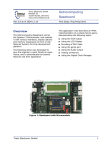
A compact (64mm x 42mm) integration board featuring
the Xilinx Spartan-3E FPGA and on-board SDRAM.
The XEM3005 is a compact USB-based FPGA integration board featuring the Xilinx Spartan-3E FPGA,
optional 32 MB 16-bit wide SDRAM, SPI configuration PROM, and two high-density 0.8-mm expansion
connectors. The USB 2.0 interface provides fast configuration downloads and FPGA-PC communication
as well as easy access with our popular FrontPanel software and developer’s API. An on-board clock
generation device has six flexible outputs available to the FPGA, SDRAM, and expansion connectors.
Software, documentation, samples, and related materials are
Copyright © 2006-2014 Opal Kelly Incorporated.
Opal Kelly Incorporated
Portland, Oregon
http://www.opalkelly.com
All rights reserved. Unauthorized duplication, in whole or part, of this document by any means except for brief
excerpts in published reviews is prohibited without the express written permission of Opal Kelly Incorporated.
Opal Kelly, the Opal Kelly Logo, and FrontPanel are trademarks of Opal Kelly Incorporated.
Linux is a registered trademark of Linus Torvalds. Microsoft and Windows are both registered trademarks of
Microsoft Corporation. All other trademarks referenced herein are the property of their respective owners and no
trademark rights to the same are claimed.
Revision History:
Date
Description
20060915
Initial release.
20070404
Added trace lengths.
20070511
Fixed resistor notes (0603, not 0608). Fixed SDRAM clocking information.
20070913
Fixed BRK3005 mechanical drawing. (was missing horizontal measurements)
20070923
Fixed entry for JP3-54 pin connection. Updated HI pin connection table in appendix.
20081004
Fixed typo for K16 FPGA pin on quick reference.
20090511
Added full SDRAM part number.
20091106
Fixed statement about programming the SPI PROM.
20140330
Replace pin list tables with reference to Pins.
Contents
Introducing the XEM3005 . . . . . . . . . . . . . . . . . . . . . . . 5
PCB Footprint. . . . . . . . . . . . . . . . . . . . . . . . . . . . . . . . . . . . . 5
BRK3005 Breakout Board. . . . . . . . . . . . . . . . . . . . . . . . 5
Functional Block Diagram. . . . . . . . . . . . . . . . . . . . . . . . . . . . 6
Power Supply. . . . . . . . . . . . . . . . . . . . . . . . . . . . . . . . . . . . . 6
Expansion Bus Power . . . . . . . . . . . . . . . . . . . . . . . . . . . 6
USB 2.0 Interface. . . . . . . . . . . . . . . . . . . . . . . . . . . . . . . . . . 6
I/O Capabilities. . . . . . . . . . . . . . . . . . . . . . . . . . . . . . . . . . . . 6
On-board Peripherals. . . . . . . . . . . . . . . . . . . . . . . . . . . . . . . 7
Serial EEPROM. . . . . . . . . . . . . . . . . . . . . . . . . . . . . . . . 7
Cypress CY22150 PLL. . . . . . . . . . . . . . . . . . . . . . . . . . . 7
SPI Serial Configuration PROM. . . . . . . . . . . . . . . . . . . . 7
Word-Wide Synchronous DRAM. . . . . . . . . . . . . . . . . . . 7
LEDs. . . . . . . . . . . . . . . . . . . . . . . . . . . . . . . . . . . . . . . . . 8
Expansion Connectors. . . . . . . . . . . . . . . . . . . . . . . . . . . . . . 8
FrontPanel Support. . . . . . . . . . . . . . . . . . . . . . . . . . . . . . . . . 8
Programmer’s Interface. . . . . . . . . . . . . . . . . . . . . . . . . . 8
Applying the XEM3005 . . . . . . . . . . . . . . . . . . . . . . . . . 9
Host Interface. . . . . . . . . . . . . . . . . . . . . . . . . . . . . . . . . . . . . 9
MUXSEL. . . . . . . . . . . . . . . . . . . . . . . . . . . . . . . . . . . . . . 10
I2C Connections. . . . . . . . . . . . . . . . . . . . . . . . . . . . . . . . 10
LEDs. . . . . . . . . . . . . . . . . . . . . . . . . . . . . . . . . . . . . . . . . . . . 11
Reconfiguration Using PROG_B . . . . . . . . . . . . . . . . . . . . . . 11
PLL Connections . . . . . . . . . . . . . . . . . . . . . . . . . . . . . . . . . . 12
SDRAM Clock . . . . . . . . . . . . . . . . . . . . . . . . . . . . . . . . . 12
JTAG. . . . . . . . . . . . . . . . . . . . . . . . . . . . . . . . . . . . . . . . . . . . 12
JP1 - JTAG Connector. . . . . . . . . . . . . . . . . . . . . . . . . . . 12
SDRAM Connections. . . . . . . . . . . . . . . . . . . . . . . . . . . . . . . 12
Clock Configuration . . . . . . . . . . . . . . . . . . . . . . . . . . . . . 13
Expansion Connectors. . . . . . . . . . . . . . . . . . . . . . . . . . . . . . 14
JP3. . . . . . . . . . . . . . . . . . . . . . . . . . . . . . . . . . . . . . . . . . 14
JP4. . . . . . . . . . . . . . . . . . . . . . . . . . . . . . . . . . . . . . . . . . 14
Setting Bank 3 I/O Voltage. . . . . . . . . . . . . . . . . . . . . . . . 15
SPI Configuration PROM. . . . . . . . . . . . . . . . . . . . . . . . . . . . 15
Booting from PROM. . . . . . . . . . . . . . . . . . . . . . . . . . . . . 15
Programming the PROM . . . . . . . . . . . . . . . . . . . . . . . . . 15
XEM3005 Mechanical Drawing. . . . . . . . . . . . . . . . . . . 16
BRK3005 Mechanical Drawing. . . . . . . . . . . . . . . . . . . 17
XEM3005 User’s Manual
4
www.opalkelly.com
XEM3005 User’s Manual
Introducing the XEM3005
The XEM3005 is a compact (64mm x 42mm, 2.52” x 1.65”) FPGA board featuring the Xilinx
Spartan-3E FPGA and a high-speed USB 2.0 interface. Designed as a full-featured integration
system, the XEM3005 provides access to 103 I/O pins on its 256-pin Spartan-3E device and has
a 32-MByte SDRAM available to the FPGA. The XEM3005 is designed to work with small to
medium-sized FPGA designs with a wide variety of external interface requirements.
PCB Footprint
A mechanical drawing of the XEM3005 is shown at the end of this manual. The PCB is 64mm
x 42mm with four mounting holes spaced as shown in the figure. These mounting holes are
electrically isolated from all signals on the XEM3005. The USB connector overhangs the PCB by
approximately 2mm in order to accommodate mounting within an enclosure.
The XEM3005 has two high-density 80-pin connectors on the top side which provide access to
many FPGA pins, power, JTAG, and the microcontroller’s I2C interface.
BRK3005 Breakout Board
A simple breakout board (the BRK3005) is provided as an optional accessory to the XEM3005.
This breakout board provides easy access to the high-density connectors on the XEM3005 by
routing them to lower-density 0.1”-spaced thru-holes. The breakout board also provides power
to the XEM3005. Typically, the user design must provide power, so the BRK3005 functions as a
convenient bootstrapping board.
A mechanical drawing of the BRK3005 is also shown at the end of this document.
www.opalkelly.com
5
XEM3005 User’s Manual
Functional Block Diagram
SPI
PROM
SDRAM
(MT48LC16M16)
USB Micro
(CY68013A)
USB
Host Interface
Bus
PLL
(CY22150)
Spartan-3E FPGA
(XC3S1200E-4FTG256)
4 LEDs
3 PLL CLKs
42 I/O
3 PLL CLK
59 I/O
2 GCLK
JP3
JP4
Power Supply
The XEM3005 is designed to be a flexible, low-cost integration module. In order to reduce cost
and better adapt to the end-user design, the XEM3005 is design without power supply capability and must be externally powered. Power must be provided as well-regulated 3.3v and 1.2v
DC supplies and can be delivered via the expansion connectors or using the 0.1”-spaced power
header. The FPGA VCCAUX supply is provided by a 2.5v regulator from 3.3v supply on the
XEM3005.
Expansion Bus Power
The USB’s 5v supply is provided to the expansion header and power header so that end-users
can design bus-powered applications. The USB 2.0 specification allows for up to 2.5 W (500mA
at 5v) to be provided to external peripherals over the USB cable. While power consumption of an
unconfigured XEM3005 is quite low, due to the flexibility allowed in FPGA design, the Spartan-3E
and SDRAM could easily consume over 2.5 W during operation with a user design, thus violating
the USB specification.
Before relying on USB power, you should be aware of the limitations and the fact that using USB
power may render the XEM3005 a USB-noncompliant device.
USB 2.0 Interface
The XEM3005 uses a Cypress CY7C68013A FX2LP USB microcontroller to make the XEM a
USB 2.0 peripheral. As a USB peripheral, the XEM is instantly recognized as a plug and play
peripheral on millions of PCs. More importantly, FPGA downloads to the XEM happen blazingly
fast, virtual instruments under FrontPanel update quickly, and data transfers are much faster than
the parallel port interfaces common on many FPGA experimentation boards.
I/O Capabilities
Depending on the FPGA device inserted on the XEM3005, the I/O pin counts will vary. The table
below indicates the number of I/O counts for each device.
6
www.opalkelly.com
XEM3005 User’s Manual
250E
500E
1200E
Inputs (+3.3v)
26
27
26
I/O (+3.3v)
24
31
32
Inputs (+VCCO3)
8
8
10
I/O (+VCCO3)
31
37
35
103
103
Totals: 89
On-board Peripherals
The XEM3005 is designed to compactly support a large number of applications with a small number of on-board peripherals. These peripherals are listed below.
Serial EEPROM
A small serial EEPROM is attached to the USB microcontroller on the XEM3005, but not directly
available to the FPGA. The EEPROM is used to store boot code for the microcontroller as well
as PLL configuration data, a unique non-mutable serial number, and a device identifier string.
The PLL configuration data is loaded from EEPROM and used to reconfigure the PLL each time
a new configuration file is loaded to the FPGA. Therefore, stable and active clocks will be present on the FPGA pins as soon as it comes out of configuration. The stored PLL configuration
may be changed at any time using FrontPanel’s PLL Configuration Dialog.
The EEPROM also stores a device identifier string which may be changed at any time using
FrontPanel. The string serves only a cosmetic purpose and is used when multiple XEM devices
are attached to the same computer so you may select the proper active device.
Cypress CY22150 PLL
A multi-output, single-PLL clock generator provides six clocks, three to the FPGA and another
three to the expansion connector JP3. The PLL is driven by a 48-MHz signal output from the
USB microcontroller. The PLL can output clocks up to 150-MHz and is configured through the
FrontPanel software interface or the FrontPanel API.
SPI Serial Configuration PROM
A 4-Mbit SPI Serial Configuration PROM (ST Microelectronics M25P40-VMN6TP) is included
on all variants of the XEM3005. This PROM allows the XEM3005 to operate without its USB
tether by automatically configuring the on-board FPGA during power-up. This PROM may be
programmed using the Opal Kelly FrontPanel Application or through API calls from your own
software.
NOTE: This feature is not yet available in FrontPanel.
Word-Wide Synchronous DRAM
The XEM optionally includes an SDRAM with a full 16-bit word-wide interface to the FPGA
(Micron MT48LC16M16A2BG-75:D or equivalent). This SDRAM is attached exclusively to the
FPGA and does not share any pins with the expansion connector. The maximum clock rate of
the SDRAM is 133 MHz.
Opal Kelly can provides different variants of the XEM3005 with different SDRAM sizes installed
(or none installed). Please contact us for more information.
www.opalkelly.com
7
XEM3005 User’s Manual
LEDs
Four LEDs are available for general use as debug outputs.
Expansion Connectors
Two high-density, 80-pin expansion connectors are available on the top-side of the XEM3005
PCB. These expansion connectors provide user access to several power rails on the XEM3005,
three clock generator outputs, two FPGA clock inputs, the USB microcontroller I2C lines, the
JTAG chain, and 101 dedicated I/O pins on the FPGA.
The connectors on the XEM3005 are Samtec BSE-040-01-F-D-A. The table below lists the appropriate Samtec mating connectors along with the total mated height.
Samtec Part Number
Mated Height
BTE-040-01-F-D-A
5.00mm (0.197”)
BTE-040-02-F-D-A
8.00mm (0.315”)
BTE-040-03-F-D-A
11.00mm (0.433”)
BTE-040-04-F-D-A
16.10mm (0.634”)
BTE-040-05-F-D-A
19.10mm (0.752”)
FrontPanel Support
The XEM3005 is fully supported by Opal Kelly’s FrontPanel software. FrontPanel augments
the limited peripheral support with a host of PC-based virtual instruments such as LEDs, hex
displays, pushbuttons, toggle buttons, and so on. Essentially, this makes your PC a reconfigurable I/O board and adds enormous value to the XEM3005 as an experimentation or prototyping
system.
Programmer’s Interface
In addition to complete support within FrontPanel, the XEM3005 is also fully supported by the
FrontPanel programmer’s interface (API), a powerful C++ class library available to Windows and
Linux programmers allowing you to easily interface your own software to the XEM.
In addition to the C++ library, wrappers have been written for Java and Python making the API
available under those languages as well. Java and Python extensions are available under Windows and Linux. Sample wrappers are also provided for Matlab and LabVIEW.
Complete documentation and several sample programs are installed with FrontPanel.
8
www.opalkelly.com
XEM3005 User’s Manual
Applying the XEM3005
Host Interface
There are 24 pins that connect the on-board USB microcontroller to the FPGA. These pins comprise the host interface on the FPGA and are used for configuration downloads. After configuration, these pins are used to allow FrontPanel communication with the FPGA.
If the FrontPanel okHostInterface module is instantiated in your design, you must map the interface pins to specific pin locations using Xilinx LOC constraints. This may be done using the
Xilinx constraints editor or specifying the constraints manually in a text file. An example is shown
below:
Xilinx constraints for okHostInterface pin mappings:
www.opalkelly.com
9
XEM3005 User’s Manual
NET
NET
NET
NET
NET
NET
NET
NET
NET
NET
NET
NET
NET
NET
NET
NET
NET
NET
NET
NET
NET
NET
NET
NET
NET
NET
“hi_in<0>”
“hi_in<1>”
“hi_in<2>”
“hi_in<3>”
“hi_in<4>”
“hi_in<5>”
“hi_in<6>”
“hi_in<7>”
“hi_out<0>”
“hi_out<1>”
“hi_inout<0>”
“hi_inout<1>”
“hi_inout<2>”
“hi_inout<3>”
“hi_inout<4>”
“hi_inout<5>”
“hi_inout<6>”
“hi_inout<7>”
“hi_inout<8>”
“hi_inout<9>”
“hi_inout<10>”
“hi_inout<11>”
“hi_inout<12>”
“hi_inout<13>”
“hi_inout<14>”
“hi_inout<15>”
LOC
LOC
LOC
LOC
LOC
LOC
LOC
LOC
LOC
LOC
LOC
LOC
LOC
LOC
LOC
LOC
LOC
LOC
LOC
LOC
LOC
LOC
LOC
LOC
LOC
LOC
=
=
=
=
=
=
=
=
=
=
=
=
=
=
=
=
=
=
=
=
=
=
=
=
=
=
“F9”;
“N5”;
“T9”;
“M7”;
“P12”;
“P11”;
“P13”;
“N12”;
“P5”;
“N10”;
“M8”;
“L8”;
“T8”;
“N8”;
“P8”;
“P9”;
“N9”;
“M9”;
“R11”;
“R6”;
“T5”;
“T4”;
“R4”;
“M6”;
“N6”;
“P6”;
Each of the samples installed with FrontPanel includes a copy of a template constraints file that
lists all the XEM3005 pins and maps them to the appropriate FPGA pins using LOC (location)
constraints. You can use this template to quickly get the pin locations correct on a new design.
MUXSEL
MUXSEL is a signal on the XEM3005 which selects the signal path to the FPGA programming
signals D0 and CCLK. When low (deasserted), the FPGA and USB microcontroller are connected. When high (asserted), the FPGA and PROM are connected.
In normal USB-programmed operation, switch JP2 is at “USB Config” pulling MUXSEL low and
connecting the FPGA and USB microcontroller at all times. This allows USB-based programming of the FPGA and subsequent USB communication with the FPGA design after configuration.
In order to allow the PROM to configure the FPGA, JP2 must be at “PROM Config”. However,
if the USB is to communicate with the FPGA post-configuration, MUXSEL must be deasserted.
Therefore, the FPGA outputs MUXSEL so that, post-configuration, the FPGA can deassert MUXSEL and communicate over USB even after the PROM has configured it.
The end result is that your FPGA design should tie HI_MUXSEL to 0. This is the case regardless
of how the design was configured (via PROM or USB). For example, in Verilog:
assign hi_muxsel = 1’b0;
I2C Connections
The FPGA is attached to the I2C lines from the USB microcontroller. In order to avoid contention
with the I2C bus, these lines should be set to high-impedance within your design. If this is not
done, FrontPanel may timeout or hang when trying to communicate with the XEM3005, particularly when programming the on-board PLL.
10
www.opalkelly.com
XEM3005 User’s Manual
The following lines in your UCF (contraints) file will attach pull-ups to the I2C lines:
NET “i2c_scl”
NET “i2c_sda”
LOC = “G16” | PULLUP;
LOC = “G15” | PULLUP;
In addition, you will need to set these signals to high-impedance in your HDL. Here is an example of how to do this in Verilog:
assign i2c_sda = 1’bz;
assign i2c_scl = 1’bz;
LEDs
There are four LEDs on the XEM3005. Each is wired directly to the FPGA according to the mapping in the table below.
The LED anodes are connected to a pull-up resistor to +3.3VDD and the cathodes wired directly
to the FPGA. To turn ON an LED, the FPGA pin should be brought low. To turn OFF an LED,
the FPGA pin should be brought high.
LED
FPGA Pin
D2
P14
D3
R13
D4
T13
D5
P15
Reconfiguration Using PROG_B
Please reference Xilinx Application Note XAPP453 for more information regarding the use of
PROG_B to force PROM-based reconfiguration.
Asserting the PROG_B signal (driving it low) to the FPGA forces the FPGA to restart its configuration process. The XEM3005 controls this signal for USB-based configuration, but the signal is
also available for user control with respect to PROM-based configuration.
PROG_B resides on the VCCAUX (+2.5v) power rail on the Spartan-3E. If you plan to control
PROG_B externally with an open-drain circuit or a momentary switch that will simply drop the
signal to ground, a direct connection to PROG_B can be made. In this case, no special considerations are necessary.
However, if the signal will be driven by a 3.3v CMOS logic signal, R11 should be replaced by a
68-Ω resistor and a shunt resistor of 250Ω should be added at R2. These considerations are
necessary because you will be driving 3.3v into an input (PROG_B) that expects 2.5v.
R11 is an 0603 resistor on the top-side of the board near JP3. By default, it is populated with a
0-Ω resistor to connect PROG_B and JP3-4.
R2 is an unpopulated 0603 resistor and is located on the bottom-side of the board near the JTAG
header JP1. It is connected between the +2.5v regulator output and DGND.
www.opalkelly.com
11
XEM3005 User’s Manual
PLL Connections
The PLL contains six output clocks. The first three are labelled SYS_CLK1 through SYS_CLK3
and are connected to the FPGA. The remaining three clocks are labelled SYS_CLK4 through
SYS_CLK6 and are connected to expansion connector JP3 The pin mapping table below details
the PLL connections.
PLL Pin
Clock Name
Connection
LCLK1
SYS_CLK1
FPGA - A8
LCLK2
SYS_CLK2
FPGA - E9
LCLK3
SYS_CLK3
FPGA - B8
LCLK4
SYS_CLK4
JP3-71
CLK5
SYS_CLK5
JP3-69
CLK6
SYS_CLK6
JP3-67
SDRAM Clock
The SDRAM clock pin (U9-F2) is connected to SYS_CLK1 which is LCLK1 on the Cypress
CY22150 PLL (U5-7). See the section on SDRAM Connections below for more details on
SDRAM clock configurations.
JTAG
JP1 - JTAG Connector
JP1 is the 2mm, 6-pin JTAG connector on-board and connects to the FPGA JTAG pins. These
pins are also mirrored to the expansion connector JP4. The JP1 pins are connected as shown
below:
JP1 Pin
Signal
1
+2.5VDD
2
TMS
3
TCK
4
TDI
5
DGND
6
TDO
SDRAM Connections
The SDRAM is connected to the 3.3v I/O on Banks 0 and 1 of the FPGA. None of these pins are
shared with the expansion connectors. The tables below list these connections.
12
www.opalkelly.com
XEM3005 User’s Manual
SDRAM Pin
FPGA Pin
SDRAM Pin
FPGA Pin
CLK
A9
A10
C15
CKE
C16
A11
A13
CS
F13
A12
B13
WE
F8
D0
A4
CAS
D11
D1
B4
RAS
E11
D2
A5
BA0
D9
D3
C3
BA1
D10
D4
C4
LDQM
B7
D5
C5
UDQM
C7
D6
D7
A0
D14
D7
E8
A1
F14
D8
E10
A2
D15
D9
B10
A3
G13
D10
A12
A4
F12
D11
E7
A5
F15
D12
A10
A6
G14
D13
C6
A7
A14
D14
A7
A8
B14
D15
D6
A9
C11
Clock Configuration
The XEM3005 has been designed to support SDRAM clocking in both “system synchronous”
and “source synchronous” modes. Both configurations are often referenced in Xilinx application notes describing SDRAM controllers and interfaces, including XAPP462: “Using DCMs in
Spartan-3”.
The block diagram below shows how the clock signals are routed on the XEM3005 PCB in the
default (factory) configuration.
SYS_CLK1
PLL
R29
SDRAM
A8 (GCLK8)
FPGA
A9 (GCLK7)
R28*
*not inserted
Expansion
(JP3)
System Synchronous from the PLL (Default Configuration)
Remove R28. Insert R29. PLL drives SYS_CLK1. This is the default configuration.
In this mode, the clock signal is sourced at the system level by the PLL on the XEM3005. The
same clock is fanned-out to both the FPGA (pin A8, GCLK8) and the SDRAM (CLK). The
FPGA, therefore considers this signal an input and synchronizes its logic fabric to it, typically using a DCM.
www.opalkelly.com
13
XEM3005 User’s Manual
System Synchronous from JP3
Insert R28. Remove R29. JP3 drives DRAM_CLK.
In this mode, the clock signal is sourced at the system level by the user design on JP3. The
same clock is fanned-out to both the FPGA (pin A9, GCLK7) and the SDRAM (CLK). The
FPGA, therefore considers this signal an input and synchronizes its logic fabric to it, typically using a DCM.
Source Synchronous
Insert R28. Remove R29. FPGA drives DRAM_CLK.
In this mode, the clock signal is sourced by the FPGA along with address and data signals to the
SDRAM. The FPGA pin A9 (GCLK7) is configured as an output and provides the clock signal
to the SDRAM. Using the DDR buffer capabilities of the Spartan-3E IOBs, the outgoing clock
edges can be perfectly synchronized with the address and data signals.
Expansion Connectors
Opal Kelly Pins is an interactive online reference for the expansion connectors on all Opal Kelly
FPGA integration modules. It provides additional information on pin capabilities, pin characteristics, and PCB routing. Additionally, Pins provides a tool for generating constraint files for place
and route tools. Pins can be found at the URL below.
http://www.opalkelly.com/pins
Also included in the Pins reference are the lengths of the PCB traces on the XEM3005. Note
that, while these lengths may be used to help equalize lengths for certain applications (like LVDS
pair matching), the XEM3005 is not an impedance-controlled PCB and was not designed specifically for LVDS use.
JP3
JP3 is an 80-pin high-density connector (Samtec BSE-040-F-D-A) providing access to FPGA
Banks 0, 1, and 2, the +3.3v and +1.2v supply rails, and the +5v from the USB.
Pins 77 and 75 are the I2C SCL and SDA pins, respectively, and connect to the I2C pins on the
Cypress USB microcontroller as well as the FPGA. Pullups are provided on the XEM3005 for
these signals.
Pins 71, 69, and 67 connect directly to the CY22150 PLL. Using FrontPanel’s PLL Configuration
Dialog, you can configure the clock signal present on these pins.
JP4
JP4 is an 80-pin high-density connector (Samtec BSE-040-F-D-A) providing access to FPGA
Banks 0, 2, and 3.
Pins 72, 74, 76, and 78 connect directly to the FPGA JTAG pins TCK, TDI, TMS, and TDO, respectively.
14
www.opalkelly.com
XEM3005 User’s Manual
Pins 41 and 42 connect directly to VCCO3 on the FPGA and provide the option of providing an
external I/O voltage to this bank. See the section below on setting the I/O voltage.
Pins 75 and 77 are connected to FPGA GCLK11 and GCLK10, respectively. These can provide
external clock input to the FPGA.
Setting Bank 3 I/O Voltage
The Spartan-3E FPGA allows users to set I/O bank voltages in order to support several different
I/O signalling standards. This functionality is supported by the XEM3005 on Bank 3 by allowing
the user to connect an independent power supply to the VCCO3 pins.
By default, a ferrite bead (FB2) has been installed which attaches VCCO3 to the +3.3VDD supply. If you intend to supply power to VCCO3, you MUST remove this ferrite bead. Power can
then be supplied through the expansion connector on pins JP4-41 and JP4-42.
SPI Configuration PROM
SPI Pin
FPGA Pin
CLK
R16
CS
P3
DIN
N16
DOUT
R15
HOLD
R10
WP
P10
Booting from PROM
In order to boot the XEM3005 from PROM, switch JP2 must be at “PROM Config”. This allows
the PROM to configure the FPGA from power-on. If your FPGA design has MUXSEL=0, the
design will still be able to communicate with FrontPanel if it is connected to a PC.
Programming the PROM
Opal Kelly’s FlashLoader sample can be used to program the PROM for untethered booting (i.e.
configuring the FPGA on power-up without the USB attached). This is a simple command-line
utility to load your bitfile into the PROM.
The source code is included with this sample to allow you to include PROM programming from
your own application. The HDL source code is not included, but the bitfile may be used along
with your application.
www.opalkelly.com
15
XEM3005 User’s Manual
XEM3005 Mechanical Drawing
4X
42.00
39.00
2.50
37.00
13.70
5.00
3.00
1.52
0
61.00
64.00
38.50
16.51
8.89
-2.03
0
3.00
0
7.53
34.33
10.50
1.57
0
-1.78
All dimensions in mm.
16
www.opalkelly.com
56.56
56.90
5.65
4.85
20.43
0
2.33
0
XEM3005 User’s Manual
81
84
72.52
60
60.04
24
28.03
9.02
0
3
BRK3005 Mechanical Drawing
2.54
0
3
8X
17.78
21.26
2.50
0.90 0.04
0.30
7.62
55.73
61
2.40
60.96
0.10
2.54
73.66
125
128
All dimensions in mm.
[inches]
www.opalkelly.com
0.10
2.54
17