1
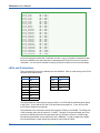
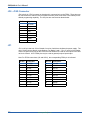
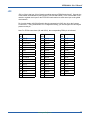
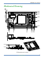
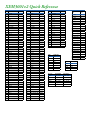
Opal Kelly XEM3001v2 User’s Manual A business-card sized (3.5’’ x 2.0’’) experimentation board featuring the Xilinx Spartan 3 FPGA. The XEM3001 is a small, business-card sized FPGA board featuring the Xilinx Spartan 3 FPGA. Designed as a bare-bones system, the XEM3001 is an excellent experimenting or prototyping system which provides access to nearly all I/O pins on the 208-pin Spartan 3 device. The USB 2.0 interface provides fast downloads and easy access with FrontPanel software. An on-board PLL provides flexible clock generation for a variety of applications and on-board pushbuttons and LEDs allow simple user interfacing when FrontPanel components don’t suit the purpose. Dozens of pins at 0.1” spacing are provided and easily fit onto a standard prototyping board with 0.1” hole spacing. Software, documentation, samples, and related materials are Copyright © 2005-2007 Opal Kelly Incorporated. Opal Kelly Incorporated 3442 SE Ironwood Ave Hillsboro, OR 97123 http://www.opalkelly.com All rights reserved. Unauthorized duplication, in whole or part, of this document by any means except for brief excerpts in published reviews is prohibited without the express written permission of Opal Kelly Incorporated. Opal Kelly, the Opal Kelly Logo, and FrontPanel are trademarks of Opal Kelly Incorporated. Linux is a registered trademark of Linus Torvalds. Microsoft and Windows are both registered trademarks of Microsoft Corporation. All other trademarks referenced herein are the property of their respective owners and no trademark rights to the same are claimed. Revision History: Date Description 20040901 Initial release. 20041103 Added PLL and JTAG (JP4) connections. 20050315 Changes for XEM3001v2. 20050420 Updated mechanical drawing. 20050507 Added functional block diagram. 20050802 Added 3D mechanical drawing. 20060222 Updated power consumption based on FX2LP device. 20070226 Updated host interface pin list for FrontPanel-3. Contents Introducing the XEM3001 . . . . . . . . . . . . . . . . . . . . . . 5 PCB Footprint . . . . . . . . . . . . . . . . . . . . . . . . . . . . . . . . . . . . . 5 Functional Block Diagram . . . . . . . . . . . . . . . . . . . . . . . . . . . . 6 Power Supply . . . . . . . . . . . . . . . . . . . . . . . . . . . . . . . . . . . . . 6 USB 2.0 Interface . . . . . . . . . . . . . . . . . . . . . . . . . . . . . . . . . . 7 On-board Peripherals . . . . . . . . . . . . . . . . . . . . . . . . . . . . . . . 7 EEPROM . . . . . . . . . . . . . . . . . . . . . . . . . . . . . . . . . . . . . 7 Cypress CY22150 PLL . . . . . . . . . . . . . . . . . . . . . . . . . . . 7 LEDs and Pushbuttons . . . . . . . . . . . . . . . . . . . . . . . . . . . 7 Expansion Connectors . . . . . . . . . . . . . . . . . . . . . . . . . . . . . . 7 FrontPanel Support . . . . . . . . . . . . . . . . . . . . . . . . . . . . . . . . . 8 Programmer’s Interface . . . . . . . . . . . . . . . . . . . . . . . . . . 8 FPGA Pin Connections . . . . . . . . . . . . . . . . . . . . . . . . 9 Host Interface . . . . . . . . . . . . . . . . . . . . . . . . . . . . . . . . . . . . . 9 LEDs and Pushbuttons . . . . . . . . . . . . . . . . . . . . . . . . . . . . . . 10 PLL Connections . . . . . . . . . . . . . . . . . . . . . . . . . . . . . . . . . . 11 JP4 - JTAG Connector . . . . . . . . . . . . . . . . . . . . . . . . . . . . . . 12 JP1 . . . . . . . . . . . . . . . . . . . . . . . . . . . . . . . . . . . . . . . . . . . . . 12 JP2 . . . . . . . . . . . . . . . . . . . . . . . . . . . . . . . . . . . . . . . . . . . . . 13 JP3 . . . . . . . . . . . . . . . . . . . . . . . . . . . . . . . . . . . . . . . . . . . . . 14 Mechanical Drawing . . . . . . . . . . . . . . . . . . . . . . . . . . 15 XEM3001v2 Quick Reference . . . . . . . . . . . . . . . . . . . 16 XEM3001v2 User’s Manual 4 www.opalkelly.com XEM3001v2 User’s Manual Introducing the XEM3001 The XEM3001 is a small, business-card sized (3.5’’ x 2.0’’) FPGA board featuring the Xilinx Spartan 3 FPGA. Designed as a full-featured starter system, the XEM3001 provides access to nearly all I/O pins on the 208-pin Spartan 3 device. The XEM3001 is ideally suited to experiments based on the FrontPanel virtual instrumentation platform, integration into prototype development, or as a quick and easy way to add USB capability to an existing device. PCB Footprint A mechanical drawing of the XEM3001 is shown below. (Dimensions are mils (1mil = 0.001”) unless otherwise noted. www.opalkelly.com 5 XEM3001v2 User’s Manual The PCB is 3.5” x 2.0” (88.9mm x 50.8mm) with four mounting holes spaced as shown in the figure. These mounting holes are electrically connected to the ground plane. The three FPGA-access ports JP1, JP2, and JP3 are located on a 0.1” grid so that the entire board may be attached to a standard prototyping board. The JTAG header JP4 is also on this grid. Functional Block Diagram ��������� ������ ��������� ��������� ������ ������ ������ �������������� ��� ��� ��������� �������������� ���������������� ���������� ���������� ��� ���������� ������ ������������� ��������� ������ ������ ������ ���������� Power Supply The XEM3001 is a bus-powered device in its default configuration (J1 jumper inserted). That is, it takes power from the 5-V USB power and generates the voltages it needs from there. To do so, the XEM3001 has small linear regulators for 3.3-V, 2.5-V, and 1.8-V. External power may be applied to any of the 3.3-V pins on JP1, JP2, or JP3 as long as the J1 jumper is removed. In this case, the 5-V USB power is not used and the device consumes no bus current. Computers and USB hubs often have USB ports that do not provide bus power. These are called unpowered ports. In order to be operated as a bus-powered device, the XEM3001 must be connected to a USB port that provides bus power. You should check with the hub or computer manufacturer to verify that the port provides bus power. The XEM3001 may also be self-powered by removing jumper J1. This jumper connects the 3.3-V regulator to the 3.3-V supply plane on the board. By removing this jumper, the 3.3-V supply and therefore the derived 2.5-V and 1.8-V supplies are disconnected from bus power. 3.3 Volts must be supplied externally (either to the device side of the jumper -- the pin closer to the “J1” marking -- or to one of the 3.3-V pins on JP1, JP2, or JP3. IMPORTANT NOTE: Under normal operating conditions and with an unconfigured FPGA, the XEM3001 draws approximately 125 mA from the 3.3-V node. FPGA current draw is impossible to predict because it strongly depends on the implemented design and clocking rates. Current requirements of the FPGA can be estimated using Xilinx power estimation tools and should be considered if you think you may be getting close to USB limits. The current can easily be measured by removing the J1 jumper and placing a current meter across the leads. If you need to exceed the 500 mA limit, make sure to apply external power and remove J1. 6 www.opalkelly.com XEM3001v2 User’s Manual WARNING: For use in bus-powered mode, always insert jumper J1 BEFORE connecting the device to the USB. USB 2.0 Interface The XEM3001 uses a Cypress CY68013 FX2 USB microcontroller to make the XEM a USB 2.0 peripheral. As a USB peripheral, the XEM is instantly recognized as a plug and play peripheral on millions of PCs. More importantly, FPGA downloads to the XEM happen blazingly fast, virtual instruments under FrontPanel update quickly, and data transfers are much faster than the parallel port interfaces common on many FPGA experimentation boards. The USB interface also allows the XEM to be bus-powered which means it is ultra-portable requiring just a USB cable and the proper drivers to connect to any supporting PC, including laptops. On-board Peripherals The XEM3001 is designed as a low-cost, barebones device. However, a few key peripherals have been added for convenience. EEPROM A small serial EEPROM is attached to the USB microcontroller on the XEM3001, but not directly available to the FPGA. The EEPROM is used to store boot code for the microcontroller as well as PLL configuration data and a device identifier string. The PLL configuration data is loaded from EEPROM and used to reconfigure the PLL each time a new configuration file is loaded to the FPGA. Therefore, stable and active clocks will be present on the FPGA pins as soon as it comes out of configuration. The stored PLL configuration may be changed at any time using FrontPanel’s PLL Configuration Dialog. The EEPROM also stores a device identifier string which may be changed at any time using FrontPanel. The string serves only a cosmetic purpose and is used when multiple XEM devices are attached to the same computer so you may select the proper active device. Cypress CY22150 PLL A multi-output, single-VCO PLL can provide up to five clocks, three to the FPGA and another two to the expansion connectors JP2 and JP3. The PLL is driven by a 48-MHz signal output from the USB microcontroller. The PLL can output clocks up to 150-MHz and is configured through the FrontPanel software interface or the FrontPanel API. LEDs and Pushbuttons Eight LEDs and four pushbuttons are available for general use as debug inputs and outputs. Expansion Connectors Three 0.1”-spaced expansion connectors (JP1, JP2, JP3) are available to connect the XEM to your devices. These connectors provide 3.3v power, ground, PLL outputs, and 88 FPGA pins for general I/O. All expansion connectors are on a 0.1” grid so that the entire XEM can piggy-back onto a standard 0.1” PCB protoboard. www.opalkelly.com 7 XEM3001v2 User’s Manual NOTE: The expansion connectors are not installed at the factory to provide you the flexibility of installing your choice of expansion -- directly soldering wires, or using stacking or right-angle connectors. FrontPanel Support The XEM3001 is fully supported by Opal Kelly’s FrontPanel software. FrontPanel augments the limited peripheral support with a host of PC-based virtual instruments such as LEDs, hex displays, pushbuttons, toggle buttons, and so on. Essentially, this makes your PC a reconfigurable I/O board and adds enormous value to the XEM3001 as an experimentation or prototyping system. Programmer’s Interface In addition to complete support within FrontPanel, the XEM3001 is also fully supported by the FrontPanel programmer’s interface (API), a powerful C++ class library available to Windows and Linux programmers allowing you to easily interface your own software to the XEM. In addition to the C++ library, wrappers have been written for Java and Python making the API available under those languages as well. Java and Python extensions are available under Windows and Linux. Complete documentation and several sample programs are installed with FrontPanel. 8 www.opalkelly.com XEM3001v2 User’s Manual FPGA Pin Connections Host Interface There are 24 pins that connect the on-board USB microcontroller to the FPGA. These pins comprise the host interface on the FPGA and are used for configuration downloads. After configuration, these pins are used to allow FrontPanel communication with the FPGA. If the FrontPanel okHostInterface module is instantiated in your design, you must map the interface pins to specific pin locations using Xilinx LOC constraints. This may be done using the Xilinx constraints editor or specifying the constraints manually in a text file. An example is shown below: Xilinx constraints for okHostInterface pin mappings: www.opalkelly.com 9 XEM3001v2 User’s Manual NET NET NET NET NET NET NET NET NET NET NET NET NET NET NET NET NET NET NET NET NET NET NET NET NET NET “hi_in<0>” “hi_in<1>” “hi_in<2>” “hi_in<3>” “hi_in<4>” “hi_in<5>” “hi_in<6>” “hi_in<7>” “hi_out<0>” “hi_out<1>” “hi_inout<0>” “hi_inout<1>” “hi_inout<2>” “hi_inout<3>” “hi_inout<4>” “hi_inout<5>” “hi_inout<6>” “hi_inout<7>” “hi_inout<8>” “hi_inout<9>” “hi_inout<10>” “hi_inout<11>” “hi_inout<12>” “hi_inout<13>” “hi_inout<14>” “hi_inout<15>” LOC LOC LOC LOC LOC LOC LOC LOC LOC LOC LOC LOC LOC LOC LOC LOC LOC LOC LOC LOC LOC LOC LOC LOC LOC LOC = = = = = = = = = = = = = = = = = = = = = = = = = = “P79”; “P57”; “P58”; “P78”; “P61”; “P62”; “P63”; “P64”; “P81”; “P85”; “P67”; “P68”; “P72”; “P74”; “P86”; “P87”; “P90”; “P92”; “P93”; “P94”; “P95”; “P96”; “P97”; “P100”; “P101”; “P102”; Each of the samples installed with FrontPanel includes a copy of a template constraints file that lists all the XEM3001 pins and maps them to the appropriate FPGA pins using LOC (location) constraints. You can use this template to quickly get the pin locations correct on a new design. LEDs and Pushbuttons There are eight LEDs and four pushbuttons on the XEM3001. Each is wired directly to the FPGA as shown in the tables below. LED FPGA Pin Button FPGA Pin D1 205 BTN1 194 D2 204 BTN2 191 D3 203 BTN3 190 D4 200 BTN4 189 D5 199 D6 198 D7 197 D8 196 The LED anodes are connected to a pull-up resistor to +3.3VDD and the cathodes wired directly to the FPGA. To turn ON an LED, the FPGA pin should be brought low. To turn OFF an LED, the FPGA pin should be brought high. The pushbuttons are connected between their respective FPGA pin and DGND. The FPGA side of the connection has a pull-up resistor to +3.3VDD. Therefore, in the pressed state, the FPGA pin will be at DGND (low) and in the unpressed state, the FPGA pin will be at +3.3VDD (high). Note that the pushbuttons are not debounced on the XEM3001. In order to deglitch the signals from the pushbuttons, proper debouncing should be done inside the FPGA. 10 www.opalkelly.com XEM3001v2 User’s Manual PLL Connections The PLL contains six output pins, one of which is left unconnected. The other five are labelled SYS_CLK1 through SYS_CLK5. SYS_CLK4 connects to JP3 and SYS_CLK5 connects to JP2. The other three pins are connected directly to the FPGA. The table below illustrates the PLL connections. PLL Pin Clock Name Connection LCLK1 SYS_CLK1 FPGA - P80 LCLK2 SYS_CLK2 FPGA - P77 LCLK3 SYS_CLK3 FPGA - P76 LCLK4 SYS_CLK4 JP3 - Pin 48 CLK5 SYS_CLK5 JP2 - Pin 3 CLK6 N/A www.opalkelly.com 11 XEM3001v2 User’s Manual JP4 - JTAG Connector JP4 is the 8-pin JTAG connector on-board and is connected only to the FPGA. These pins can be connected to an external JTAG command converter (such as the Xilinx JTAG cables) for additional programming capability. The JP4 pins are connected as shown below: JP4 Pin Signal 1 +2.5VDD 2 TCK 3 DGND 4 TMS 5 DGND 6 TDI 7 DGND 8 TDO JP1 JP1 is a 20-pin dual-row 100-mil header, four pins of which are dedicated to power supply. The other 16 pins connect directly to the Spartan 3 on Banks 0 and 1. Pins 17 and 18 of the header connect to global clock pins on the FPGA and can therefore be used as clock inputs to the internal clock network. All 16 FPGA pins may be used as general-purpose input/output. Note: For FPGA connections (I/O and GCLK), the corresponding FPGA pin is indicated. 12 JP1 Pin Connection JP1 Pin Connection 1 +3.3VDD 11 I/O 169 2 +3.3VDD 12 I/O 168 3 I/O 187 13 I/O 167 4 I/O 185 14 I/O 166 5 I/O 182 15 I/O 165 6 I/O 178 16 I/O 162 7 I/O 176 17 I/O / GCLK6 183 8 I/O 175 18 I/O / GCLK5 181 9 I/O 172 19 DGND 10 I/O 171 20 DGND www.opalkelly.com XEM3001v2 User’s Manual JP2 JP2 is a 50-pin dual-row 100-mil header providing access to FPGA Banks 6 and 7. Several pins of this header are dedicated to power supply (+3.3VDD and DGND). Pin 4 of this header is connected to a global clock input on the FPGA and can therefore be used as an input to the global clock network. Pin 3 on this header is SYSCLK5 and is directly connected to LCLK5 (pin 14) on the Cypress CY22150 PLL. Using FrontPanel’s PLL Configuration Dialog, you can configure the clock signal present on this pin. Note: For FPGA connections (I/O and GCLK), the corresponding FPGA pin is indicated. JP2 Connection Pin JP2 Connection Pin JP2 Connection Pin 1 DGND 18 I/O 20 35 I/O 37 2 DGND 19 DGND 36 I/O 39 3 SYS CLK 5 20 DGND 37 I/O 40 4 I/O / GCLK7 184 21 I/O 21 38 I/O 42 5 I/O 5 22 I/O 22 39 I/O 43 6 I/O 7 23 I/O 24 40 I/O 44 7 I/O 9 24 I/O 26 41 +3.3VDD 8 I/O 10 25 I/O 27 42 +3.3VDD 9 +3.3VDD 26 I/O 28 43 I/O 45 10 +3.3VDD 27 I/O 29 44 I/O 46 11 I/O 11 28 I/O 31 45 I/O 48 12 I/O 12 29 I/O 33 46 I/O 50 13 I/O 13 30 I/O 34 47 I/O 51 14 I/O 15 31 DGND 48 I/O 52 15 I/O 16 32 DGND 49 DGND 16 I/O 18 33 I/O 35 50 DGND 17 I/O 19 34 I/O 36 www.opalkelly.com 13 XEM3001v2 User’s Manual JP3 JP3 is a 50-pin dual-row 100-mil header providing access to FPGA Banks 2 and 3. Several pins of this header are dedicated to power supply (+3.3VDD and DGND). Pin 47 of this header is connected to a global clock input on the FPGA and can therefore be used as an input to the global clock network. Pin 48 on this header is SYSCLK4 and is directly connected to LCLK4 (pin 12) on the Cypress CY22150 PLL. Using FrontPanel’s PLL Configuration Dialog, you can configure the clock signal present on this pin. Note: For FPGA connections (I/O and GCLK), the corresponding FPGA pin is indicated. 14 JP3 Connection Pin JP3 Connection Pin JP3 Connection Pin 1 DGND 18 I/O 139 35 I/O 122 2 DGND 19 DGND 36 I/O 120 3 I/O 156 20 DGND 37 I/O 119 4 I/O 155 21 I/O 138 38 I/O 117 5 I/O 154 22 I/O 137 39 I/O 116 6 I/O 152 23 I/O 135 40 I/O 115 7 I/O 150 24 I/O 133 41 +3.3VDD 8 I/O 149 25 I/O 132 42 +3.3VDD 9 +3.3VDD 26 I/O 131 43 I/O 114 10 +3.3VDD 27 I/O 130 44 I/O 113 11 I/O 148 28 I/O 128 45 I/O 111 12 I/O 147 29 I/O 126 46 I/O 109 13 I/O 146 30 I/O 125 47 I/O / GCLK4 180 14 I/O 144 31 DGND 48 SYS CLK 4 15 I/O 143 32 DGND 49 DGND 16 I/O 141 33 I/O 124 50 DGND 17 I/O 140 34 I/O 123 www.opalkelly.com XEM3001v2 User’s Manual Mechanical Drawing www.opalkelly.com 15 XEM3001v2 Quick Reference JP2 Connection JP3 Connection 1 DGND YBUS 1 DGND XBUS JP1 Connection 1 +3.3VDD 2 DGND 2 DGND 3 SYS CLK 5 3 I/O 156 0 4 I/O / GCLK7 184 YCLK1 4 I/O 155 5 I/O 5 35 5 6 I/O 7 34 7 I/O 9 8 I/O 10 9 10 11 I/O 11 12 ZBUS 2 +3.3VDD 3 I/O 187 0 1 4 I/O 185 1 I/O 154 2 5 I/O 182 2 6 I/O 152 3 6 I/O 178 3 33 7 I/O 150 4 7 I/O 176 4 32 8 I/O 149 5 8 I/O 175 5 +3.3VDD 9 +3.3VDD 9 I/O 172 6 +3.3VDD 10 +3.3VDD 10 I/O 171 7 31 11 I/O 148 6 11 I/O 169 8 I/O 12 30 12 I/O 147 7 12 I/O 168 9 13 I/O 13 29 13 I/O 146 8 13 I/O 167 10 14 I/O 15 28 14 I/O 144 9 14 I/O 166 11 15 I/O 16 27 15 I/O 143 10 15 I/O 165 12 16 I/O 18 26 16 I/O 141 11 16 I/O 162 13 17 I/O 19 25 17 I/O 140 12 17 I/O / GCLK6 183 ZCLK1 18 I/O 20 24 18 I/O 139 13 18 I/O / GCLK5 181 ZCLK2 19 DGND 19 DGND 19 DGND 20 DGND 20 DGND 20 DGND 21 I/O 21 23 21 I/O 138 14 22 I/O 22 22 22 I/O 137 15 23 I/O 24 21 23 I/O 135 16 24 I/O 26 20 24 I/O 133 17 25 I/O 27 19 25 I/O 132 18 26 I/O 28 18 26 I/O 131 19 27 I/O 29 17 27 I/O 130 20 28 I/O 31 16 28 I/O 128 21 29 I/O 33 15 29 I/O 126 22 30 I/O 34 14 30 I/O 125 23 31 DGND 31 DGND 32 DGND 32 DGND 33 I/O 35 13 33 I/O 124 24 34 I/O 36 12 34 I/O 123 25 35 I/O 37 11 35 I/O 122 26 36 I/O 39 10 36 I/O 120 27 PLL Pin Clock Name Connection 37 I/O 40 9 37 I/O 119 28 LCLK1 SYS_CLK1 FPGA - P80 38 I/O 42 8 38 I/O 117 29 LCLK2 SYS_CLK2 FPGA - P77 39 I/O 43 7 39 I/O 116 30 LCLK3 SYS_CLK3 FPGA - P76 40 I/O 44 6 40 I/O 115 31 LCLK4 SYS_CLK4 JP3 - Pin 48 41 +3.3VDD 41 +3.3VDD CLK5 SYS_CLK5 JP2 - Pin 3 42 +3.3VDD 42 +3.3VDD CLK6 N/A 43 I/O 45 5 43 I/O 114 32 44 I/O 46 4 44 I/O 113 33 45 I/O 48 3 45 I/O 111 34 46 I/O 50 2 46 I/O 109 35 47 I/O 51 1 47 I/O / GCLK4 180 XCLK1 48 I/O 52 0 48 SYS CLK 4 49 DGND 49 DGND 50 DGND 50 DGND Host Interface Pin FPGA Pin HI_IN[0] 79 HI_IN[1] 57 HI_IN[2] 58 HI_IN[3] 78 HI_IN[4] 61 HI_IN[5] 62 HI_IN[6] 63 HI_IN[7] 64 HI_OUT[0] 81 HI_OUT[1] 85 HI_INOUT[0] 67 HI_INOUT[1] 68 HI_INOUT[2] 72 HI_INOUT[3] 74 HI_INOUT[4] 86 HI_INOUT[5] 87 HI_INOUT[6] 90 HI_INOUT[7] 92 HI_INOUT[8] 93 HI_INOUT[9] 94 HI_INOUT[10] 95 HI_INOUT[11] 96 HI_INOUT[12] 97 HI_INOUT[13] 100 HI_INOUT[14] 101 HI_INOUT[15] 102 LED FPGA Pin D1 205 D2 204 D3 203 D4 200 Button FPGA Pin D5 199 BTN1 194 D6 198 BTN2 191 D7 197 BTN3 190 D8 196 BTN4 189